EP3354698B1 - Composition d'encre pour frittage photonique et son procédé de production - Google Patents
Composition d'encre pour frittage photonique et son procédé de production Download PDFInfo
- Publication number
- EP3354698B1 EP3354698B1 EP16860139.1A EP16860139A EP3354698B1 EP 3354698 B1 EP3354698 B1 EP 3354698B1 EP 16860139 A EP16860139 A EP 16860139A EP 3354698 B1 EP3354698 B1 EP 3354698B1
- Authority
- EP
- European Patent Office
- Prior art keywords
- metal
- melting point
- capping layer
- ink composition
- copper
- Prior art date
- Legal status (The legal status is an assumption and is not a legal conclusion. Google has not performed a legal analysis and makes no representation as to the accuracy of the status listed.)
- Active
Links
Images




Classifications
-
- C—CHEMISTRY; METALLURGY
- C09—DYES; PAINTS; POLISHES; NATURAL RESINS; ADHESIVES; COMPOSITIONS NOT OTHERWISE PROVIDED FOR; APPLICATIONS OF MATERIALS NOT OTHERWISE PROVIDED FOR
- C09D—COATING COMPOSITIONS, e.g. PAINTS, VARNISHES OR LACQUERS; FILLING PASTES; CHEMICAL PAINT OR INK REMOVERS; INKS; CORRECTING FLUIDS; WOODSTAINS; PASTES OR SOLIDS FOR COLOURING OR PRINTING; USE OF MATERIALS THEREFOR
- C09D11/00—Inks
- C09D11/52—Electrically conductive inks
-
- H—ELECTRICITY
- H01—ELECTRIC ELEMENTS
- H01B—CABLES; CONDUCTORS; INSULATORS; SELECTION OF MATERIALS FOR THEIR CONDUCTIVE, INSULATING OR DIELECTRIC PROPERTIES
- H01B1/00—Conductors or conductive bodies characterised by the conductive materials; Selection of materials as conductors
- H01B1/20—Conductive material dispersed in non-conductive organic material
- H01B1/22—Conductive material dispersed in non-conductive organic material the conductive material comprising metals or alloys
-
- C—CHEMISTRY; METALLURGY
- C09—DYES; PAINTS; POLISHES; NATURAL RESINS; ADHESIVES; COMPOSITIONS NOT OTHERWISE PROVIDED FOR; APPLICATIONS OF MATERIALS NOT OTHERWISE PROVIDED FOR
- C09D—COATING COMPOSITIONS, e.g. PAINTS, VARNISHES OR LACQUERS; FILLING PASTES; CHEMICAL PAINT OR INK REMOVERS; INKS; CORRECTING FLUIDS; WOODSTAINS; PASTES OR SOLIDS FOR COLOURING OR PRINTING; USE OF MATERIALS THEREFOR
- C09D5/00—Coating compositions, e.g. paints, varnishes or lacquers, characterised by their physical nature or the effects produced; Filling pastes
- C09D5/24—Electrically-conducting paints
-
- H—ELECTRICITY
- H01—ELECTRIC ELEMENTS
- H01B—CABLES; CONDUCTORS; INSULATORS; SELECTION OF MATERIALS FOR THEIR CONDUCTIVE, INSULATING OR DIELECTRIC PROPERTIES
- H01B1/00—Conductors or conductive bodies characterised by the conductive materials; Selection of materials as conductors
- H01B1/14—Conductive material dispersed in non-conductive inorganic material
- H01B1/16—Conductive material dispersed in non-conductive inorganic material the conductive material comprising metals or alloys
-
- H—ELECTRICITY
- H01—ELECTRIC ELEMENTS
- H01B—CABLES; CONDUCTORS; INSULATORS; SELECTION OF MATERIALS FOR THEIR CONDUCTIVE, INSULATING OR DIELECTRIC PROPERTIES
- H01B13/00—Apparatus or processes specially adapted for manufacturing conductors or cables
-
- H—ELECTRICITY
- H01—ELECTRIC ELEMENTS
- H01B—CABLES; CONDUCTORS; INSULATORS; SELECTION OF MATERIALS FOR THEIR CONDUCTIVE, INSULATING OR DIELECTRIC PROPERTIES
- H01B13/00—Apparatus or processes specially adapted for manufacturing conductors or cables
- H01B13/0036—Details
-
- H—ELECTRICITY
- H01—ELECTRIC ELEMENTS
- H01B—CABLES; CONDUCTORS; INSULATORS; SELECTION OF MATERIALS FOR THEIR CONDUCTIVE, INSULATING OR DIELECTRIC PROPERTIES
- H01B5/00—Non-insulated conductors or conductive bodies characterised by their form
- H01B5/14—Non-insulated conductors or conductive bodies characterised by their form comprising conductive layers or films on insulating-supports
-
- H—ELECTRICITY
- H05—ELECTRIC TECHNIQUES NOT OTHERWISE PROVIDED FOR
- H05K—PRINTED CIRCUITS; CASINGS OR CONSTRUCTIONAL DETAILS OF ELECTRIC APPARATUS; MANUFACTURE OF ASSEMBLAGES OF ELECTRICAL COMPONENTS
- H05K1/00—Printed circuits
- H05K1/02—Details
- H05K1/09—Use of materials for the conductive, e.g. metallic pattern
- H05K1/092—Dispersed materials, e.g. conductive pastes or inks
- H05K1/097—Inks comprising nanoparticles and specially adapted for being sintered at low temperature
Definitions
- the present invention relates to an ink composition for photonic sintering, and more particularly, to an ink composition for photonic sintering capable of producing a conductive thin film having excellent sintering ability even when irradiated with extremely low intensity light to thereby have excellent electrical conductivity, improved moisture resistance, and excellent binding force with a substrate, and a preparation method thereof.
- the ink including the metal nanoparticle has an advantage of simplifying a process by printing metal wiring having a fine pattern on various substrates through single printing processes such as screen printing, inkjet printing, gravure offset printing, reverse offset printing, etc., without using a complicated process of photolithography.
- the production cost may be remarkably reduced due to simplification of the process, and a highly integrated and highly efficient printed circuit may be produced by refinement of a wiring width.
- Document US 2015/053464 A1 shows a method of manufacturing a conductive metal thin film, the method including: a) heating and stirring a first solution containing a metal precursor, acid, amine, and a reducing agent to synthesize metal nano-particles on which formation of a surface oxide film is suppressed; b) dispersing the metal nano-particles synthesize in step a) in a non-aqueous solvent to prepare a conductive ink composition; c) applying the conductive ink composition onto an insulating substrate; and d) heat-treating the insulating substrate applied with the ink composition to form a conductive metal thin film.
- KR 2015 0118801 A shows a conductive copper composite ink for light sintering and a light sintering method using the same, which comprises: a nano-sized first copper particle; a second copper particle composed of one species or a mixture thereof selected from a micro-sized copper particle and a copper nanowire; and a polymer binder resin.
- compositions are known from US 2013/288892 A1 , EP 2 130 627 A1 , US 2008/087137 A1 and WO 2014/112683 A1 .
- the present applicant focused that conductivity of a metal wiring is deteriorated by a surface oxide film present in a metal nanoparticle in a metal nanoparticle-based ink, and provided a method of synthesizing a metal nanoparticle in which formation of the surface oxide film is completely controlled ( Korean Patent Laid-Open Publication No. 10-2013-0111180 ).
- Korean Patent Laid-Open Publication No. 10-2013-0111180 Korean Patent Laid-Open Publication No.
- 10-2013-0111180 filed by the present applicant has a limitation that an ink containing the metal nanoparticle in which the surface oxide film is controlled is applied to perform thermal sintering, and in order to impart bulk characteristics through the thermal sintering, a high-temperature heat treatment should be performed for a long period of time, specifically 2 hours, at a high temperature of 300°C or higher in an inert atmosphere.
- the high-temperature heat treatment over a long period of time has difficulty in using a flexible polymer substrate that is spotlighted as a substrate of a flexible element, and further, it is disadvantageous in a roll-to-roll continuous process having excellent commercial properties.
- an ink composition containing a copper nanoparticle has a high melting point of 1000°C or higher, high energy should be applied when producing a conductive thin film using the ink composition, and the produced conductive thin film has low moisture resistance in a high temperature and high humidity environment, and thus specific resistance is rapidly increased.
- An object of the present invention is to provide an ink composition for photonic sintering capable of producing a conductive thin film having excellent sintering ability even when irradiated with extremely low intensity light to thereby have excellent electrical conductivity, improved moisture resistance, and excellent binding force with a substrate, and a preparation method thereof.
- an ink composition for photonic sintering includes: a metal nanoparticle including a first metal satisfying the following Relational Expression 1; a non-aqueous organic binder; and a non-aqueous solvent.
- a preparation method of an ink composition for photonic sintering includes: a) synthesizing a metal nanoparticle including a first metal satisfying the following Relational Expression 1 by heating and stirring a reaction solution including a metal precursor, an organic acid, an amine-based compound, and a reducing agent; and b) preparing a dispersion in which the metal nanoparticle and a non-aqueous organic binder are dispersed in a non-aqueous solvent.
- the ink composition for photonic sintering and the preparation method thereof according to the present invention may have the following advantages in production of a conductive thin film.
- photonic sintering through extremely low light energy with an intensity in which a polymer binder remains on a metal thin film without being carbonized may be performed, and thus it is possible to produce a conductive metal thin film having a significantly excellent electrical conductivity comparable to that of a bulk and having a significantly excellent binding force with a substrate.
- the conductive thin film may be produced by a photonic sintering process which is excellent in thermal stability, and thus it is possible to prevent a substrate from being damaged even if the substrate has a low upper temperature limit.
- the present applicant intensified study of a metal nanoparticle in which formation of a surface oxide film is controlled proposed in Korean Patent Laid-Open Publication No. 10-2013-0111180 , and as a result, found that when photonic sintering an ink composition containing the metal nanoparticle in which a surface oxide film is controlled, a metal thin film having electrical conductivity comparable to that of a bulk could be produced by remarkably low light energy.
- an ink composition for photonic sintering may include a firt metal nanoparticle including a first metal, the first metal nanoparticle being capped with a first capping layer including an organic acid, the first capping layer substantially completely preventing the first metal from formation of a surface oxide film, wherein the first metal is copper, silver, gold, nickel, tin, aluminum, or an alloy thereof, a low melting point metal particle capped with a third capping layer including an organic acid substantially completely preventing formation of a surface oxide film, the low melting point metal having a melting point of 800°C or lower;; a non-aqueous organic binder; and a non-aqueous solvent.
- the first metal nanoparticle will be satisfying the following Relational Expression 1: A 1 / A 2 ⁇ 0.2 in Relational Expression 1, A 1 /A 2 is a ratio in which a first metal 2p 3/2 peak area (A 1 ) of an oxide of the first metal is divided by a first metal 2p 3/2 peak area (A 2 ) of the first metal, in X-ray photoelectron spectroscopy spectrum on a surface of the first metal.
- the X-ray photoelectron spectroscopy spectrum may be measured using an Al K ⁇ source at a degree of vacuum of 10 -8 or less, and a first metal 2p 3/2 peak of a first metal and a first metal 2p 3/2 peak of a first metal oxide may be extracted, thereby calculating a degree of oxidation through an area ratio between two peaks.
- the first metal is substantially completely prevented from formation of a surface oxide film.
- a 1 /A 2 may be more preferably 0.01 or less.
- the first metal 2p 3/2 peak of the oxide of the first metal is not substantially shown, and thus A 1 /A 2 may be substantially zero.
- the first metal particle is capped with the first capping layer including a first organic acid, and thus formation of the surface oxide film is controlled, and the formation of the surface oxide film is substantially completely prevented.
- the first metal is any one or two or more selected from among copper, silver, gold, nickel, tin, aluminum, or an alloy thereof, preferably copper.
- Copper is a metal having good electrical conductivity after silver, has very good electrical conductivity, and is economical since it is able to be easily supplied and received at a low price.
- an average diameter of the first metal nanoparticle including the first metal may be 20 to 300 nm, more preferably 50 to 300 nm.
- the metal nanoparticles may be tightly packed with each other to be uniformly sintered without a non-sintered region at the time of photonic sintering.
- a shape of the first metal nanoparticle is not particularly limited, but may be an angular polygonal shape, a columnar shape, a spherical shape, or a mixed shape thereof.
- the ink composition for photonic sintering comprises: a first metal nanoparticle including a first metal, wherein the first metal nanoparticle is a core-shell nanostructure including the first metal as a core, wherein the first metal is substantially completely prevented from formation of a surface oxide film; a second metal shell surrounding the core; and a second capping layer surrounding the second metal shell; a low melting point metal particle capped with a third capping layer including an organic acid substantially completely preventing formation of a surface oxide film, the low melting point metal having a melting point of 800°C or lower; a non-aqueous organic binder; and a non-aqueous solvent, wherein the first metal is copper, silver, gold, nickel, tin, aluminum, or an alloy thereof.
- the metal nanoparticle may be a nanostructure having a core-shell form, including a first metal in which formation of a surface oxide film is controlled as a core and a second metal surrounding the core and forming a solid solution with the first metal.
- An ink composition containing the metal nanoparticle may be photonic sintered to form a solid solution in which the first metal and the second metal form a completely uniform phase even though light having an extremely low light quantity is irradiated.
- the first metal core may satisfy the above-described Relational Expression 1, and the formation of the surface oxide film is substantially completely prevented.
- the second metal shell is capped by the capping layer, and thus formation of a surface oxide film is controlled, and the formation of a surface oxide film is substantially completely prevented.
- the second metal shell may satisfy the following Relational Expression 3, more preferably A 11/ A 12 may be 0.01 or less, and may reach substantially 0 since a 2p 3/2 peak of the second metal oxide is not substantially shown.
- a 11/ A 12 is a ratio in which a second metal 2p 3/2 peak area (A 11 ) of an oxide of the second metal is divided by a second metal 2p 3/2 peak area (A 12 ) of the second metal, in X-ray photoelectron spectroscopy spectrum on a surface of the second metal shell.
- the X-ray photoelectron spectroscopy spectrum may be measured using an Al K ⁇ source at a degree of vacuum of 10 -8 or less, and a second metal 2p 3/2 peak of the second metal and a second metal 2p 3/2 peak of the second metal oxide may be extracted, thereby calculating a degree of oxidation through an area ratio between two peaks.
- the ink composition for photonic sintering according to the second embodiment of the present invention may include a core-shell nanostructure including a first metal satisfying Relational Expression 1 as a core, a second metal shell surrounding the core and satisfying Relational Expression 3, and a capping layer surrounding the second metal shell.
- the ink composition for photonic sintering according to the second embodiment of the present invention may include the core-shell nanostructure satisfying Relational Expressions 1 and 3 to thereby have a remarkably excellent sintering ability even at the time of photonic sintering by light irradiation with an extremely low light quantity.
- the ink composition for photonic sintering has the core-shell shape in which the second metal shell surrounds the first metal core, the first metal and the second metal in the ink composition may be distributed in a uniform ratio, and thus even at the time of photonic sintering by light irradiation with an extremely low light quantity, respective metals may be easily connected to each other and uniformly mixed to form a more perfect solid solution.
- the solid solution refers to a material in which atoms of two or more different elements are homogeneously mixed, and is formed when another atom is added to a base material and an existing base material lattice structure is maintained without forming a new structure.
- the solid solution may mean that the second metal is penetrated into the first metal, which is the base material, to form a single-phase solution.
- the solid solution is a second metal atom that is penetrated into the first metal which is the base material, and may be divided into an intrusion type and a substitution type depending on its form.
- the intrusion type may be a type in which the second metal atom is interposed between first metal lattice structures, and the intrusion type solid solution may be formed when an atomic radius of the second metal atom is significantly smaller than that of the first metal atom.
- the substitution type may be a type in which the second metal atom is substituted with the first metal atom, and the substitution type solid solution may be formed when it is difficult to interpose the second metal atom between the first metal lattice structures since the atomic radius of the second metal atom is similar to that of the first metal atom.
- the solid solution may control physical properties depending on the kind and content of the first metal and the second metal, and thus it is possible to control the kind and the content of the first metal and the second metal according to the physical properties required by the conductive thin film to be produced after photonic sintering.
- the solid solution may be divided into a complete solid solution and a limited solid solution.
- the complete solid solution may be formed regardless of a content of the first metal and the second metal, and has an advantage in that the content is able to be freely controlled according to desired physical properties.
- the second metal may not be penetrated into the first metal at a specific content or more, that is, a solubility limit is determined, and thus a content ratio of the first metal and the second metal may be controlled within a content range at which the solid solution is capable of being formed.
- the first metal core is copper, silver, gold, nickel, tin, aluminum, or an alloy thereof.
- the second metal may form a solid solution with the first metal, may maintain excellent electrical conductivity at the time of forming the solid solution, and may be selected from metals capable of improving physical properties such as moisture resistance, corrosion resistance, etc.
- the second metal shell is copper, silver, gold, nickel, tin, aluminum or an alloy thereof, wherein the first metal core and the second metal shell are different metals.
- the first metal core may be copper and the second metal shell may be nickel.
- the ink composition for photonic sintering may include a core-shell nanostructure including a copper core satisfying Relational Expression 1; a nickel shell surrounding the copper core and satisfying Relational Expression 3; and a capping layer surrounding the nickel shell.
- Copper and nickel may have the same face centered cubic (FCC) and may have similar atomic radius, electron affinity, and valence electron number, thereby forming the complete solid solution. Accordingly, physical properties of the conductive thin film may be controlled by freely controlling the content of copper and nickel. In particular, by using copper having excellent electrical conductivity and nickel having excellent oxidation stability, it is possible to produce a photonic sintered conductive thin film having excellent electrical conductivity and improved moisture resistance.
- FCC face centered cubic
- a molar ratio between copper and nickel may be 1 : 0.1 to 1, and more preferably 1 : 0.3 to 0.6.
- the conductive thin film produced after photonic sintering may effectively maintain the electrical conductivity and effectively improve the moisture resistance, thereby suppressing a rapid increase in specific resistance in a high temperature and high humidity environment.
- a resistance change (R/Ro) of the conductive thin film may be remarkably suppressed to 1.2 times or less the initial resistance in a high temperature and high humidity environment of humidity of 85% /temperature of 85°C.
- R/Ro is a resistance after 24 hours
- R 0 is a resistance of the initial conductive thin film.
- a 1 /A 2 in Relational Expression 1 is a ratio in which a Cu 2p 3/2 peak area (A 1 ) of an oxide of copper is divided by a Cu 2p 3/2 peak area (A 2 ) of copper, in X-ray photoelectron spectroscopy spectrum on a surface of the copper core.
- X-ray photoelectron spectroscopy spectrum may be measured under 920-960 eV binding energy condition using an Al K ⁇ source at a degree of vacuum of 10 -8 or lower, and Cu 2p 3/2 peaks of copper and copper oxide may be extracted, thereby calculating a degree of oxidation through an area ratio between two peaks.
- a 11 /A 12 in Relational Expression 3 is a ratio in which a Ni 2p 3/2 peak area (A 11 ) of an oxide of nickel is divided by a Ni 2p 3/2 peak area (A 12 ) of nickel, in X-ray photoelectron spectroscopy spectrum on a surface of the nickel shell.
- X-ray photoelectron spectroscopy spectrum may be measured under 840-860 eV binding energy condition using an Al K ⁇ source at a degree of vacuum of 10 -8 or lower, and Ni 2p 3/2 peaks of nickel and nickel oxide may be extracted, thereby calculating a degree of oxidation through an area ratio between two peaks.
- the second metal shell according to the second embodiment of the present invention is capped with a capping layer, and more specifically, the capping layer may contain an organic acid. Since the organic acid may be preferentially chemisorbed onto the second metal shell to form a dense organic acid film, the capping layer may be formed of the organic acid. That is, the capping layer may be a film of the organic acid that is chemisorbed onto the second metal shell. However, as described below in the preparation method of an ink composition, a small amount of amine may be included in the capping layer in a production process using the organic acid and the organic amine together. As the second metal shell is capped with the capping layer including the organic acid, formation of the surface oxide film of the second metal shell may be prevented.
- the organic acid may have at least one of a straight chain form, a branched form or a cyclic form having 6 to 30 carbon atoms, and may be one or two or more selected from saturated or unsaturated organic acids. More specifically, the organic acid may be one or two or more selected from the group consisting of oleic acid, lysine oleic acid, stearic acid, hydroxystearic acid, linoleic acid, aminodecanoic acid, hydroxydecanoic acid, lauric acid, decenoic acid, undecenoic acid, palmitoleic acid, hexyldecanoic acid, hydroxypalmitic acid, hydroxymyristic acid, hydroxydecanoic acid, palmitoleic acid, and myristoleic acid, etc., but is not limited thereto.
- the capping layer for capping the second metal shell may have a thickness of 1 to 2 nm.
- an effect of preventing the formation of the oxide film may be reduced.
- the thickness of the capping layer is extremely thick, excessive energy and time may be consumed for removing the capping layer which is an organic material in the production of the metal thin film using the ink composition including the core-shell nanostructure.
- the ink composition for photonic sintering according to the second embodiment of the present invention may include the core-shell nanostructure including the first metal core satisfying Relational Expression 1 and the second metal shell surrounding the first metal core, and thus it is possible to form a perfect solid solution having remarkably excellent sintering ability even at the time of photonic sintering by light irradiation with an extremely low light quantity.
- the ink composition of the present invention further includes a metal having a relatively lower melting point than that of the metal nanoparticle in order to have significantly excellent sintering ability in spite of light irradiation with extremely low intensity at the time of photonic sintering, secure significantly excellent electrical conductivity and binding force with a substrate, and improve flowability of the metal, thereby completely performing the sintering process even with lower light energy.
- the ink composition of the present invention further includes a low melting point metal having a melting point of 800°C or lower.
- the low melting point metal in the present invention has a relatively low melting point as compared to that of the metal nanoparticle, and specifically has a melting point of 800°C or lower, more specifically, a melting point of 150 to 800°C, and may be a single metal or an alloy of two or more metals.
- the ink composition may have significantly excellent sintering ability even though light irradiation is performed with an extremely low intensity at the time of photonic sintering the ink composition, and the photonic sintering through an extremely low light energy with an intensity in which the polymer binder remains on the metal thin film without being carbonized may be performed, thereby producing a conductive metal thin film not only having a significantly excellent electrical conductivity comparable to that of a bulk, but also having a significantly excellent binding force with a substrate.
- the low melting point metal may be more easily melted as compared to the metal nanoparticle by light irradiation. Due to this property, flowability of the metal may be improved even at the time of light irradiation with extremely low energy to thereby produce a conductive thin film which is uniformly and well photonic sintered over the entire region, even in a non-sintered region, and the produced conductive thin film may have significantly excellent electrical conductivity.
- thermal stability may be excellent, and thus even if a substrate has a very low upper temperature limit of 200°C or lower, the substrate may be prevented from being damaged in a step of forming a conductive thin film, and a conductive thin film having excellent electrical conductivity even if it is any substrate may be formed.
- the low melting point metal has a relatively low melting point as compared to the metal nanoparticle.
- the low melting point metal may include an alloy composed of two or more metals selected from copper, tin, silver, bismuth, zinc, indium, and lead.
- the kind and the content of the low melting point metal may be controlled in consideration of physical properties required for the conductive thin film to be produced.
- an alloy containing the same metal as the metal nanoparticle is preferably the low melting point metal.
- the metal nanoparticle and the low melting point metal may be more easily fused at the time of photonic sintering, thereby having excellent sintering ability.
- the same metal as the low melting point metal may be contained and the metal nanoparticle may be affected, and thus the sintering may be more effectively performed even with lower energy injection.
- the low melting point metal when the metal nanoparticle is copper, the low melting point metal may be a copper-tin-based alloy.
- a melting point of copper is about 1,083°C, and when an alloy is produced by mixing tin together with copper, an alloy having a melting point significantly lower than that of a single copper metal may be obtained.
- the melting point of the copper-tin-based alloy depends on how a ratio of the two metals is controlled.
- copper and tin are mixed so as to have a melting point of 800°C or lower.
- the copper-tin-based alloy may satisfy the following Chemical Formula 1: [Chemical Formula 1] Cu 1 Sn x in Chemical Formula 1, x is 0.1 ⁇ x ⁇ 2.
- an average diameter of the copper-tin-based alloy may be less than 0.414 times the average diameter of the metal nanoparticle.
- the copper-tin-based alloy may be interposed between the metal nanoparticles in the above-described size range to thereby maximize a particle filling effect, and thus light sintering ability may be further improved.
- the average diameter of the copper-tin-based alloy may be 5 to 300 nm, and more preferably 20 to 200 nm.
- the metal nanoparticle and the copper-tin-based alloy may be tightly packed, and may be uniformly sintered at the time of photonic sintering in non-sintered region when irradiated with extremely low intensity light, and the flowability of the metal may be effectively improved.
- a shape of the copper-tin-based alloy is not particularly limited, but may be an angular polygonal shape, a columnar shape, a spherical shape, a core-shell shape, or a mixed shape thereof.
- the copper-tin-based alloy may be added in a content of 0.1 to 50 parts by weight based on 100 parts by weight of the metal nanoparticle, but the content thereof is not necessarily limited thereto. Mixing in the above-described range may prevent deterioration of electrical conductivity and mechanical properties of the conductive thin film.
- the low melting point metal is provided as a low melting point metal particle capped with a third capping layer including an organic acid substantially completely preventing formation of a surface oxide film.
- the low melting point metal may also be synthesized, as described below, by the same production method as the metal nanoparticle to thereby be capped with the third capping layer including an organic acid, and thus the formation of the surface oxide film is substantially completely prevented.
- the low melting point metal may satisfy the following Relational Expression 4, and more preferably A 21 /A 22 may be 0.01 or less.
- the 2p 3/2 peak of the oxide of the low melting point metal is not substantially shown, and thus A 21 /A 22 may be substantially zero.
- the metal 2p 3/2 peak area (A 21 ) of the oxide of the low melting point metal may be the sum of metal 2p 3/2 peak areas of oxides of the respective metals contained in the low melting point metal
- the metal 2p 3/2 peak area (A 22 ) of the low melting point metal may be the sum of metal 2p 3/2 peak areas of the respective metals contained in the low melting point metal.
- the ink composition for photonic sintering according to claim 1 or claim 5 may be effectively performed without damaging the substrate even when irradiated with light having extremely low light quantity, and further, surprisingly, the ink composition may be sintered so as to have electrical conductivity comparable to that of the bulk even in a state in which the polymer binder is not carbonized but remains while maintaining original physical properties of the polymer binder.
- the ink composition for photonic sintering may produce a conductive thin film by light irradiation with extremely low energy satisfying the following Relational Expression 2: I LS ⁇ I c
- I LS is energy (J/cm 2 ) of light irradiated onto the coating film
- I c is the maximum energy (J/cm 2 ) of light in which an organic substrate is not deteriorated.
- a conductive thin film having an electrical conductivity comparable to that of the bulk in the state in which the non-aqueous organic binder contained in the ink is not carbonized but remains on a thin film while maintaining physical properties of the binder itself, preventing deterioration of a low-cost transparent polymer substrate such as polyethersulfone (PES), polyethylene naphthalate (PEN), polyethylene terephthalate (PET), or the like, and having remarkable binding force with the substrate.
- PES polyethersulfone
- PEN polyethylene naphthalate
- PET polyethylene terephthalate
- the production method of the conductive thin film according to the present invention may have a characteristic constitution in which a light quantity of light that is sintered to have electrical conductivity comparable to that of the bulk is lower than a light quantity of light that does not deteriorate the organic substrate without carbonizing the polymer binder.
- the method is advantageous in that it is possible to produce a conductive metal thin film having excellent electrical conductivity comparable to that of bulk without damaging the substrate even if the substrate has a very low upper temperature limit of 100°C or less, and it is possible to produce a conductive metal thin film which is very suitable for flexible components since binding force between the metal thin film and the substrate is extremely excellent due to the remaining polymer binder.
- the photonic sintering process may be used, it is possible to produce a film having a large area in a very short time in the atmosphere, which is an advantage of the photonic sintering, and a roll-to-roll process may be implemented, and thus commerciality may be excellent, the process may be simplified, and production cost may be reduced.
- the light irradiated onto the coating film may vary depending on characteristics of the ink composition for photonic sintering.
- the metal nanoparticle included in the ink composition for photonic sintering is a core-shell nanostructure
- a conductive thin film may be produced through light irradiation with an extremely low energy.
- the metal nanoparticle may be a core-shell nanostructure including the first metal as the core, the second metal shell surrounding the core; and the capping layer surrounding the second metal shell.
- the ink composition for photonic sintering including a core-shell nanostructure composed of a copper core and a nickel shell
- the ink composition may be sintered through light irradiation with an extremely low light quantity of 2.6 J/cm 2 or less to form the perfect solid solution, and thus the conductive thin film produced from the ink composition may have excellent electrical conductivity and improved moisture resistance.
- the ink composition for photonic sintering further includes a low melting point metal having a melting point of 800°C or less
- the conductive thin film having excellent electrical conductivity may be produced by irradiating light onto the coating film so as to satisfy Relational Expression 2.
- the conductive ink for photonic sintering further includes a low melting point metal having a melting point of 800°C or less, light having an energy of 1.3 J/cm 2 or less may be irradiated.
- the ink composition may be sintered through light irradiation with an extremely low energy of 1.3 J/cm 2 or less, and may have excellent photonic sintering ability, thereby having excellent electrical conductivity.
- the ink composition according to the present invention includes a non-aqueous organic binder and a non-aqueous solvent as described above.
- the non-aqueous organic binder is not particularly limited, but may be any non-aqueous organic binder material that is conventionally used to improve physical binding force of the coating film when preparing the conductive ink.
- the non-aqueous organic binder may be one or two or more selected from polyvinylidene fluoride (PVDF), polymethylmethacrylate (PMMA), self-crosslinkable acrylic resin emulsion, hydroxyethyl cellulose, ethylhydroxyethyl cellulose, carboxymethyl cellulose, hydroxycellulose, methylcellulose, nitrocellulose, ethylcellulose, styrene butadiene rubber (SBR), a copolymer of C1-C10alkyl(meth)acrylate and unsaturated carboxylic acid, gelatin, thixoton, starch, polystyrene, polyurethane, a resin including a carboxylic group, a phenolic resin, a mixture of e
- PVDF polyviny
- the non-aqueous organic binder may be a non-aqueous polymer material having an amine value of 5 to 150 mgKOH/g.
- the non-aqueous polymer material may simultaneously perform a role of a binder and a dispersant.
- the non-aqueous organic binder may be a copolymer of an unsaturated carboxylic acid or a graft polymer thereof, and may be a copolymer of an unsaturated carboxylic acid or a graft polymer thereof having an amine value of 5 to 150 mgKOH/g.
- the non-aqueous organic binder does not interfere with binding between the metal particles at the time of photonic sintering, while simultaneously acting as the binder and the dispersant, and thus a metal thin film that is more compact and has excellent conductivity may be produced.
- the copolymer of unsaturated carboxylic acid or the graft polymer thereof having an amine value of 5 to 150 mg KOH/g may include a copolymer of C1-C10alkyl(meth)acrylate and unsaturated carboxylic acid, a copolymer of polyetherketone and unsaturated carboxylic acid, a copolymer of polyacrylamide and unsaturated carboxylic acid, a copolymer of polyethylene oxide and unsaturated carboxylic acid, a copolymer of polyethylene glycol and unsaturated carboxylic acid or a mixture thereof.
- the copolymer of unsaturated carboxylic acid or the graft polymer thereof having an amine value of 5 to 150 mg KOH/g may have
- non-aqueous organic binder a commercial product containing the non-aqueous organic binder material may be used.
- the non-aqueous organic binder may include BYK130, BYK140, BYK160, BYK161, BYK162, BYK163, BYK164, BYK165, BYK167, BYK169, BYK170, BYK171, BYK174 EFKA 4610, EFKA 4644, EFKA 4654, EFKA 4665, EFKA 4620, EFKA 4666, EFKA 4642, or the like, but the non-aqueous organic binder is not limited thereto.
- the non-aqueous solvent is not particularly limited, but preferably may be one or two or more selected from the group consisting of alkane having 6 to 30 carbon atoms, amine, toluene, xylene, chloroform, dichloromethane, tetradecane, octadecene, chlorobenzene, dichlorobenzene, chlorobenzoic acid, and dipropylene glycol propyl ether, and a content thereof may be controlled so as to have suitable fluidity for coating or printing.
- the ink composition for photonic sintering may contain 0.05 to 5 parts by weight of the non-aqueous organic binder and 20 to 800 parts by weight of the non-aqueous solvent, based on 100 parts by weight of the metal nanoparticle.
- the non-aqueous organic binder may remain on the conductive metal thin film without impairing inherent physical properties thereof at the time of photonic sintering. Accordingly, when the content of the non-aqueous organic binder in the conductive ink composition is extremely high, densification between the metal nanoparticles may be inhibited by the polymer binder that binds between the metal nanoparticles or between the metal nanoparticle and the substrate.
- a content range of 0.05 to 5 parts by weight of the non-aqueous organic binder based on the particles may be a range in which the densification between metal nanoparticles may not be interfered, and a coating film having physical strength in which a shape is stably maintained when the applied ink composition is dried and having excellent binding force with a substrate may be formed, and at the same time, the binding force between the substrate metal thin films may be remarkably improved by the polymer binder remaining on the metal thin film after photonic sintering.
- the conductive ink composition may contain 20 to 800 parts by weight of a non-aqueous solvent to have proper fluidity for coating or printing even though it may vary to some extent depending on an application method of the conductive ink composition.
- Another aspect of the present invention relates to preparation methods of an ink composition for photonic sintering according to claims 8 and 9.
- the preparation method of an ink composition for photonic sintering may include: a) synthesizing a first metal nanoparticle including a first metal the first metal nanoparticle being capped with a first capping layer including an organic acid, the first capping layer substantially completely preventing the first metal from formation of a surface oxide film by heating and stirring a reaction solution including a metal precursor, an organic acid, an amine-based compound, and a reducing agent; and b) preparing a dispersion in which the metal nanoparticle, a low melting point metal particle capped with a third capping layer including an organic acid, the low melting point metal having a melting point of 800°C or lower and the third capping layer substantially completely preventing formation of a surface oxide film and a non-aqueous organic binder are dispersed in a non-aqueous solvent.
- the first metal nanoparticle may satisfy the following Relational Expression 1, A 1 / A 2 ⁇ 0.2 in Relational Expression 1, A 1 /A 2 is a ratio in which a first metal 2p 3/2 peak area (A 1 ) of an oxide of the first metal is divided by a first metal 2p 3/2 peak area (A 2 ) of the first metal, in X-ray photoelectron spectroscopy spectrum on a surface of the first metal.
- step a) preparing of the first metal nanoparticle capped with the capping layer may be performed with reference to Korean Patent Laid-Open Publication No. 10-2013-0111180 filed by the present applicant, and the entire disclosure of which is incorporated herein by reference.
- step a) includes preparing the first metal nanoparticle including the first metal that prevents a surface oxide film from being formed and is capped with the first capping layer by heating a reaction solution including a metal precursor, an organic acid, an amine-based compound and a reducing agent.
- the heating and stirring may be performed in an inert atmosphere.
- the first capping layer contains an organic acid. Since the organic acid may be preferentially chemisorbed onto the first metal particle to form a dense organic acid film, the first capping layer may be formed of the organic acid. That is, the capping layer may be a film of the organic acid that is chemisorbed onto the first metal particle included in the metal nanoparticle. However, a small amount of amine may be included in the capping layer in the production process using an organic acid and an amine-based compound together. As the first metal particle is capped with the first capping layer including the organic acid, formation of the surface oxide film of the first metal particle may be prevented.
- the metal of the metal precursor is to form the first metal nanoparticle including the first metal, and is one or two or more selected from the group consisting of copper, silver, gold, nickel, tin, aluminum and an alloy thereof.
- the metal precursor may be one or more inorganic salts selected from the group consisting of nitrate, sulfate, acetate, phosphate, silicate and hydrochloride of a metal selected from the group consisting of copper, silver, gold, nickel, tin, aluminum and an alloy thereof.
- the organic acid may have at least one of a straight chain form, a branched form or a cyclic form having 6 to 30 carbon atoms, and may be one or two or more selected from saturated or unsaturated acids. More specifically, the organic acid may be one or two or more selected from the group consisting of oleic acid, lysine oleic acid, stearic acid, hydroxystearic acid, linoleic acid, aminodecanoic acid, hydroxydecanoic acid, lauric acid, decenoic acid, undecenoic acid, palmitoleic acid, hexyldecanoic acid, hydroxypalmitic acid, hydroxymyristic acid, hydroxydecanoic acid, palmitoleic acid, and myristoleic acid, etc., but is not limited thereto.
- a molar ratio of the metal precursor and the organic acid may be 1 (metal precursor) : 0.2 to 4 (acid).
- the amine-based compound may have at least one of a straight chain form, a branched form or a cyclic form having 6 to 30 carbon atoms, and may be one or two or more selected from saturated and unsaturated amine. More specifically, the amine-based compound may be selected from hexylamine, heptylamine, octylamine, dodecylamine, 2-ethylhexylamine, 1,3-dimethyl-n-butylamine, and 1-aminotridecane, etc., but is not limited thereto.
- a content of the amine-based compound in the first solution is 0.2 mol or more, preferably 1 to 50 mol, and more preferably 5 to 50 mol based on 1 mol of the metal precursor, but the upper limit is not limited since the amine-based compound may act as the non-aqueous solvent.
- the reducing agent may be one or two or more selected from hydrazine-based reducing agents including hydrazine, hydrazine anhydride, hydrazine hydrochloride, hydrazine sulfate, hydrazine hydrate, and phenylhydrazine. Further, in addition thereto, the reducing agent may be one or two or more selected from hydride-based; borohydride-based including tetrabutylammonium borohydride, tetramethylammonium borohydride, tetraethylammonium borohydride, and sodium borohydride, etc.; sodium phosphate-based; and ascorbic acid. In the first solution, the reducing agent may be included so that a molar ratio of the reducing agent and the metal precursor is 1 to 100.
- the synthesizing of the metal nanoparticle is not significantly limited, but in consideration of a reduction efficiency, the synthesizing of the metal nanoparticle may be performed at 80 to 300°C, more preferably 100 to 250°C, and further more preferably 130 to 200°C, and may be performed in an inert atmosphere.
- the metal nanoparticle may be separated and recovered by a conventional method used when recovering the nanoparticle, such as centrifugation.
- the step of synthesizing a first metal nanoparticle including a first metal includes a-1) synthesizing a first metal core, the first metal core being capped with a first capping layer substantially completely preventing formation of a surface oxide film by heating and stirring a first solution including a first metal precursor, a first organic acid, a first amine-based compound, and a first reducing agent; and a-2) synthesizing a core-shell nanostructure having a structure in which the first metal core, a second metal shell, and a second capping layer are sequentially positioned from inside to outside by heating and stirring the first metal core, and a second solution including a second metal precursor, a second organic acid, a second amine-based compound, and a second reducing agent.
- the first metal core may satisfy the following Relational Expression 1: A 1 / A 2 ⁇ 0.2 in Relational Expression 1, A 1 /A 2 is a ratio in which a first metal 2p 3/2 peak area (A 1 ) of an oxide of the first metal is divided by a first metal 2p 3/2 peak area (A 2 ) of the first metal, in X-ray photoelectron spectroscopy spectrum on a surface of the first metal.
- step a-1 is a step of preparing a first metal core that prevents a surface oxide film from being formed and is capped with a first capping layer by heating a first solution including a first metal precursor, a first organic acid, a first amine-based compound and a first reducing agent, wherein the heating and stirring may be performed in an inert atmosphere.
- the first capping layer may contain the first organic acid. Since the first organic acid may be preferentially chemisorbed onto the first metal to form a dense organic acid film, the first capping layer may be formed of the first organic acid. That is, the first capping layer may be a film of the first organic acid that is chemisorbed onto the first metal. However, a small amount of amine may be included in the first capping layer in the production process using the first organic acid and the first amine-based compound together. As the first metal is capped with the first capping layer including the first organic acid, formation of the surface oxide film of the first metal particle may be prevented.
- the metal of the first metal precursor is one or two or more selected from the group consisting of copper, silver, gold, nickel, tin, aluminum and an alloy thereof.
- the first metal precursor may be one or more inorganic salts selected from the group consisting of nitrate, sulfate, acetate, phosphate, silicate, and hydrochloride of a metal selected from the group consisting of copper, silver, gold, nickel, tin, aluminum, and an alloy thereof.
- the first organic acid may have at least one of a straight chain form, a branched form or a cyclic form having 6 to 30 carbon atoms, and may be one or two or more selected from saturated or unsaturated acids. More specifically, the first organic acid may be one or two or more selected from the group consisting of oleic acid, lysine oleic acid, stearic acid, hydroxystearic acid, linoleic acid, aminodecanoic acid, lauric acid, decenoic acid, undecenoic acid, hexyldecanoic acid, hydroxypalmitic acid, hydroxymyristic acid, hydroxydecanoic acid, palmitoleic acid, and myristoleic acid, etc., but is not limited thereto.
- a molar ratio of the first metal precursor and the first organic acid may be 1 (metal precursor) : 0.2 to 4 (acid).
- the first amine-based compound may have at least one of a straight chain form, a branched form or a cyclic form having 6 to 30 carbon atoms, and may be one or two or more selected from saturated and unsaturated amine. More specifically, the first amine-based compound may be selected from hexylamine, heptylamine, octylamine, dodecylamine, 2-ethylhexylamine, 1,3-dimethyl-n-butylamine, and 1-aminotridecane, etc., but is not limited thereto.
- a content of the first amine-based compound in the first solution is 0.2 mol or more, preferably 1 to 50 mol, and more preferably 5 to 50 mol based on 1 mol of the first metal precursor, but the upper limit is not necessarily limited since the first amine-based compound may act as the non-aqueous solvent.
- the first reducing agent may be one or two or more selected from hydrazine-based reducing agents including hydrazine, hydrazine anhydride, hydrazine hydrochloride, hydrazine sulfate, hydrazine hydrate, and phenylhydrazine. Further, in addition thereto, the first reducing agent may be one or two or more selected from hydride-based; borohydride-based including tetrabutylammonium borohydride, tetramethylammonium borohydride, tetraethylammonium borohydride, and sodium borohydride, etc.; sodium phosphate-based; and ascorbic acid. In the first solution, the first reducing agent may be included so that a molar ratio of first reducing agent and the first metal precursor is 1 to 100.
- the synthesizing of the first metal nanoparticle is not significantly limited, but in consideration of a reduction efficiency, the synthesizing of the first metal nanoparticle may be performed at 80 to 300°C, more preferably 100 to 250°C, and further more preferably 130 to 200°C, and may be performed in an inert atmosphere.
- the first metal nanoparticle may be separated and recovered by a conventional method used when recovering the nanoparticle, such as centrifugation.
- step a-2 may be performed.
- step a-2) is a step of preparing a core-shell nanostructure having a structure in which the first metal core satisfying Relational Expression 1, a second metal shell, and a second capping layer are sequentially positioned from inside to outside by heating the first metal core, and a second solution including a second metal precursor, a second organic acid, a second amine-based compound, and a second reducing agent, wherein the heating and stirring may be performed in an inert atmosphere.
- the formation of the surface oxide film is substantially completely prevented.
- the 2p 3/2 peak of the first metal oxide may not be substantially shown, and thus A 1 /A 2 may be substantially zero. That is, the first metal core does not have the surface oxide film formed thereon, and thus the first metal may be in direct contact with the second metal.
- the second capping layer may contain the second organic acid. Since the second organic acid may be preferentially chemisorbed onto the second metal shell to form a dense organic acid film, the second capping layer may be formed of the second organic acid. That is, the second capping layer may be a film of the second organic acid that is chemisorbed onto the second metal shell. However, a small amount of amine may be included in the first capping layer in the production process using the second organic acid and the second amine-based compound together. As the second metal shell is capped with the second capping layer including the second organic acid, formation of the surface oxide film of the second metal shell may be prevented.
- the second metal shell may be capped by the second capping layer to control the formation of the surface oxide film, and the formation of the surface oxide film is substantially and completely prevented.
- the second metal shell may satisfy the following Relational Expression 3, and more preferably A 11/ A 12 may be 0.01 or less.
- the 2p 3/2 peak of the second metal oxide is not substantially shown, and thus A 11/ A 12 may reach substantially zero.
- a 11/ A 12 is a ratio in which a second metal 2p 3/2 peak area (A 11 ) of an oxide of the second metal is divided by a second metal 2p 3/2 peak area (A 12 ) of the second metal, in X-ray photoelectron spectroscopy spectrum on a surface of the second metal shell.
- the X-ray photoelectron spectroscopy spectrum may be measured using an Al K ⁇ source at a degree of vacuum of 10 -8 or less, and a second metal 2p 3/2 peak of the second metal and a second metal 2p 3/2 peak of the second metal oxide may be extracted, thereby calculating a degree of oxidation through an area ratio between two peaks.
- the metal of the second metal precursor is one or two or more selected from the group consisting of copper, silver, gold, nickel, tin, aluminum and an alloy thereof, which is different from the kind of the first metal.
- the second metal precursor may be one or more inorganic salts selected from the group consisting of nitrate, sulfate, acetate, phosphate, silicate and hydrochloride of a metal selected from the group consisting of copper, silver, gold, nickel, tin, aluminum and an alloy thereof.
- the second metal precursor may be added in a content of 0.1 to 1 mol based on 1 mol of the first metal nanoparticle.
- the second organic acid may have at least one of a straight chain form, a branched form or a cyclic form having 6 to 30 carbon atoms, and may be one or two or more selected from saturated or unsaturated acids. More specifically, the second organic acid may be one or two or more selected from the group consisting of oleic acid, lysine oleic acid, stearic acid, hydroxystearic acid, linoleic acid, aminodecanoic acid, hydroxydecanoic acid, lauric acid, decenoic acid, undecenoic acid, palmitoleic acid, hexyldecanoic acid, hydroxypalmitic acid, hydroxymyristic acid, hydroxydecanoic acid, palmitoleic acid, and myristoleic acid, etc., but is not limited thereto, and may be the same as or different from the first organic acid.
- a molar ratio of the second metal precursor and the second organic acid may be 1 (metal precursor) :
- the second reducing agent may be one or two or more selected from hydrazine-based reducing agents including hydrazine, hydrazine anhydride, hydrazine hydrochloride, hydrazine sulfate, hydrazine hydrate, and phenylhydrazine.
- the second reducing agent may be one or two or more selected from hydride-based; borohydride-based including tetrabutylammonium borohydride, tetramethylammonium borohydride, tetraethylammonium borohydride, and sodium borohydride, etc.; sodium phosphate-based; and ascorbic acid, and may be the same as or different from the first reducing agent.
- the second reducing agent may be included so that a molar ratio of the second reducing agent and the second metal precursor is 1 to 100.
- the synthesizing of the core-shell nanostructure is not significantly limited, but in consideration of a reduction efficiency, the synthesizing of the core-shell nanostructure may be performed at 100 to 350°C, more preferably 140 to 300°C, and further more preferably 180 to 280°C, and may be performed in an inert atmosphere.
- the core-shell nanostructure may be separated and recovered by a conventional method used when recovering the nanoparticle, such as centrifugation.
- the ink composition for photonic sintering may be prepared by dispersing the metal nanoparticle together with a non-aqueous organic binder in a non-aqueous solvent.
- the non-aqueous organic binder is not particularly limited, but may be any non-aqueous organic binder material that is conventionally used to improve physical binding force of the coating film when preparing the conductive ink.
- the non-aqueous organic binder may be one or two or more selected from polyvinylidene fluoride (PVDF), polymethylmethacrylate (PMMA), self-crosslinkable acrylic resin emulsion, hydroxyethyl cellulose, ethylhydroxyethyl cellulose, carboxymethyl cellulose, hydroxycellulose, methylcellulose, nitrocellulose, ethylcellulose, styrene butadiene rubber (SBR), a copolymer of C1-C10alkyl(meth)acrylate and unsaturated carboxylic acid, gelatin, thixoton, starch, polystyrene, polyurethane, a resin including a carboxylic group, a phenolic resin, a mixture of e
- PVDF polyviny
- the non-aqueous organic binder does not interfere with binding between the metal particles at the time of photonic sintering, while simultaneously acting as the binder and the dispersant, and thus a metal thin film that is more compact and has excellent conductivity may be produced.
- the copolymer of unsaturated carboxylic acid or the graft polymer thereof having an amine value of 5 to 150 mg KOH/g may include a copolymer of C1-C10alkyl(meth)acrylate and unsaturated carboxylic acid, a copolymer of polyetherketone and unsaturated carboxylic acid, a copolymer of polyacrylamide and unsaturated carboxylic acid, a copolymer of polyethylene oxide and unsaturated carboxylic acid, a copolymer of polyethylene glycol and unsaturated carboxylic acid or a mixture thereof.
- the copolymer of unsaturated carboxylic acid or the graft polymer thereof having an amine value of 5 to 150 mg KOH/g may have
- non-aqueous organic binder a commercial product containing the non-aqueous organic binder material may be used.
- the non-aqueous organic binder may include BYK130, BYK140, BYK160, BYK161, BYK162, BYK163, BYK164, BYK165, BYK167, BYK169, BYK170, BYK171, BYK174 EFKA 4610, EFKA 4644, EFKA 4654, EFKA 4665, EFKA 4620, EFKA 4666, EFKA 4642, or the like, but the non-aqueous organic binder is not limited thereto.
- the non-aqueous solvent is not particularly limited, but preferably may be one or two or more selected from the group consisting of alkane having 6 to 30 carbon atoms, amine, toluene, xylene, chloroform, dichloromethane, tetradecane, octadecene, chlorobenzene, dichlorobenzene, chlorobenzoic acid, and dipropylene glycol propyl ether.
- the ink composition for photonic sintering may contain 0.05 to 5 parts by weight of the non-aqueous organic binder and 20 to 800 parts by weight of the non-aqueous solvent, based on 100 parts by weight of the metal nanoparticle.
- a content range of 0.05 to 5 parts by weight of the non-aqueous organic binder based on the particles may be a range in which the densification between metal nanoparticles may not be interfered, and a coating film having physical strength in which a shape is stably maintained when the applied ink composition is dried and having excellent binding force with a substrate may be formed, and at the same time, the binding force between the substrate metal thin films may be remarkably improved by the polymer binder remaining in the metal thin film after photonic sintering.
- the dispersion of step b) further includes the low melting point metal having a melting point of 800°C or lower in the form of a low melting point metal particle capped with a third capping layer including an organic acid.
- the ink composition for photonic sintering may contain 0.1 to 50 parts by weight of a low-melting point metal, 0.05 to 5 parts by weight of a non-aqueous organic binder and 20 to 800 parts by weight of a non-aqueous solvent, based on 100 parts by weight of the metal nanoparticle.
- the low melting point metal having a melting point of 800°C or lower may be prepared by a method similar to that of the metal nanoparticle.
- the low melting point metal to be prepared may be obtained in the same manner as the metal nanoparticle except that a precursor and a content thereof are changed according to the kind of the metal to be mixed.
- the low melting point metal that prevents a surface oxide film from being formed and is capped with a third capping layer by heating a third solution including a precursor of a low melting point metal to be prepared, a third organic acid, a third amine-based compound, and a third reducing agent.
- the heating and stirring may be performed in an inert atmosphere.
- the third capping layer contains the third organic acid. Since the third organic acid may be preferentially chemisorbed onto the low melting point metal particle to form a dense organic acid film, the third capping layer may be formed of the third organic acid. That is, the third capping layer may be a film of the organic acid that is chemisorbed onto the low melting point metal particle. However, a small amount of amine may be included in the third capping layer in the production process using the third organic acid and the third amine-based compound together. As the low melting point metal is capped with the third capping layer including the third organic acid, formation of the surface oxide film of the low melting point metal may also be prevented.
- the precursor of the low melting point metal to be prepared may be two or more kinds.
- the metal of the precursor of the low melting point metal may be two or more selected from copper, tin, silver, bismuth, zinc, indium and lead.
- the precursor of the low melting point metal may be one or more inorganic salts selected from the group consisting of nitrate, sulfate, acetate, phosphate, silicate and hydrochloride of two or more metals selected from the group consisting of copper, tin, silver, bismuth, zinc, indium and lead.
- the selected metal is copper and tin
- respective precursors may be inorganic salts that are the same as or different from each other.
- the precursor of the low melting point metal may be a copper salt and a tin salt.
- the third organic acid may have at least one of a straight chain form, a branched form or a cyclic form having 6 to 30 carbon atoms, and may be one or two or more selected from saturated or unsaturated acids. More specifically, the third organic acid may be one or two or more selected from the group consisting of oleic acid, lysine oleic acid, stearic acid, hydroxystearic acid, linoleic acid, aminodecanoic acid, hydroxydecanoic acid, lauric acid, decenoic acid, undecenoic acid, palmitoleic acid, hexyldecanoic acid, hydroxypalmitic acid, hydroxymyristic acid, hydroxydecanoic acid, palmitoleic acid, and myristoleic acid, etc., but is not limited thereto.
- a molar ratio of the precursor of the low melting point metal and the third organic acid may be 1 (precursor of low melting point metal) : 0.2 to 4 (a
- the third amine-based compound may have at least one of a straight chain form, a branched form or a cyclic form having 6 to 30 carbon atoms, and may be one or two or more selected from saturated and unsaturated amine. More specifically, the third amine-based compound may be selected from hexylamine, heptylamine, octylamine, dodecylamine, 2-ethylhexylamine, 1,3-dimethyl-n-butylamine, and 1-aminotridecane, etc., but is not limited thereto.
- a content of the third amine-based compound in the third solution is 0.2 mol or more, preferably 1 to 50 mol, and more preferably 5 to 50 mol based on 1 mol of the precursor of the low melting point metal, but the upper limit is not limited since the third amine-based compound may act as the non-aqueous solvent.
- the third reducing agent may be one or two or more selected from hydrazine-based reducing agents including hydrazine, hydrazine anhydride, hydrazine hydrochloride, hydrazine sulfate, hydrazine hydrate, and phenylhydrazine. Further, in addition thereto, the third reducing agent may be one or two or more selected from hydride-based; borohydride-based including tetrabutylammonium borohydride, tetramethylammonium borohydride, tetraethylammonium borohydride, and sodium borohydride, etc.; sodium phosphate-based; and ascorbic acid. In the third solution, the third reducing agent may be included so that a molar ratio of the third reducing agent and the precursor of the low melting point metal is 1 to 100.
- the synthesizing of the low melting point metal nanoparticle is not significantly limited, but in consideration of a reduction efficiency, the synthesizing of the low melting point metal nanoparticle may be performed at 100 to 350°C, more preferably 140 to 300°C, and further more preferably 180 to 280°C, and may be performed in an inert atmosphere.
- the low melting point metal nanoparticle may be separated and recovered by a conventional method used when recovering the nanoparticle, such as centrifugation.
- Still another aspect of the present invention relates to a production method of a photonic sintering conductive thin film and a photonic sintering conductive thin film produced therefrom according to claim 10.
- the production method of a photonic sintering conductive thin film includes: A) preparing an ink composition for photonic sintering as described above; B) applying the ink composition for photonic sintering to a substrate to form a coating film; and C) irradiating the coating film with visible light having energy of 1.3 J/cm2 or less in a wavelength band of 400 to 800 nm to produce a conductive thin film, thereby producing a conductive thin film.
- the coating film may satisfy the following Relational Expression 2: I LS ⁇ I c wherein in Relational Expression 2, I LS is energy (J/cm 2 ) of light irradiated onto the coating film, and I c is the maximum energy (J/cm 2 ) of light in which an organic substrate is not deteriorated.
- step A) may be performed by the same method as step a) and step b).
- step B) of applying the ink composition for photonic sintering to a substrate to form a coating film may be performed.
- the applying of the ink composition for photonic sintering may be performed by a method of coating or printing.
- the coating may be performed by dip coating, spin coating, spray coating, casting, or the like
- the printing may be performed by screen printing, inkjet printing, hydrostatic printing, microcontact printing, imprinting, gravure printing, reverse offset printing, gravure offset printing, or the like.
- the applying of the ink composition for photonic sintering may be applied to have an appropriate pattern according to design of a product to be manufactured, and selectively, after the ink composition for photonic sintering may be applied to a transparent polymer substrate, drying for volatilizing the solvent may be performed before the light irradiation.
- the production method according to an embodiment of the present invention may produce a conductive thin film through an extremely low light energy, and as a result, as shown in the following Examples, a conductive thin film having significantly excellent electrical conductivity even on the polyethylene terephthalate substrate requiring an extremely low processing temperature may be produced.
- the substrate may be any substrate as long as it is a substrate having insulation property.
- the substrate may include an organic substrate such as polyethylene terephthalate, polyethylene naphthalate, polyetheretherketone, polycarbonate, polyarylate, polyether sulfone, polyimide, or the like, an inorganic substrate such as glass, paper, or the like.
- a step of irradiating the coating film with light to produce a conductive thin film may be performed.
- sintering of the metal nanoparticle at the time of photonic sintering is achieved by instantaneous melting of a surface area of metal nanoparticles due to high energy applied by light.
- light substantially having a light quantity of 10 J/cm 2 or more is irradiated.
- the ink composition for photonic sintering according to the present invention when used, sintering may be effectively performed without damaging the substrate even when light having extremely low light intensity is irradiated. Further, surprisingly, the ink composition may be sintered so as to have electrical conductivity comparable to that of the bulk even in a state in which the polymer binder is not carbonized but remains while maintaining original physical properties of the polymer binder.
- a conductive thin film having an electrical conductivity comparable to that of the bulk in the state in which the non-aqueous organic binder contained in the ink is not carbonized but remains on a thin film while maintaining physical properties of the binder itself, preventing deterioration of a low-cost transparent polymer substrate such as polyethersulfone (PES), polyethylene naphthalate (PEN), polyethylene terephthalate (PET), or the like, and having remarkable binding force with the substrate.
- PES polyethersulfone
- PEN polyethylene naphthalate
- PET polyethylene terephthalate
- This photonic sintering condition has not been known and has not been studied in the field of a production method of metal wiring using photonic sintering according to the related art, and is a condition that is only obtained when photonic sintering the ink composition containing the metal nanoparticle including the first metal satisfying Relational Expression 1.
- the production method of the conductive thin film according to the present invention may have a characteristic constitution in which a light quantity of light that is sintered so as to have electrical conductivity comparable to that of the bulk is lower than a light quantity of light that does not deteriorate the organic substrate even without carbonizing the polymer binder.
- the method is advantageous in that it is possible to produce a conductive metal thin film having excellent electrical conductivity comparable to that of the bulk without damaging the substrate even if the substrate has a very low upper temperature limit of 100°C or less, and it is possible to produce a conductive metal thin film which is very suitable for flexible components since binding force between the metal thin film and the substrate is excellent due to the remaining polymer binder.
- the photonic sintering process may be used, it is possible to produce a film having a large area in a very short time under the atmosphere environment, which is an advantage of the photonic sintering, and a roll-to-roll process may be implemented, and thus commerciality may be excellent, the process may be simplified, and production cost may be reduced.
- the light irradiated onto the coating film may vary depending on characteristics of the ink composition for photonic sintering.
- the metal nanoparticle included in the ink composition for photonic sintering in step A) is a core-shell nanostructure
- a conductive thin film may be produced through light irradiation with an extremely low energy.
- the metal nanoparticle may be a core-shell nanostructure including the first metal as the core, the second metal shell surrounding the core; and the capping layer surrounding the second metal shell.
- a perfect solid solution may be formed, and a conductive metal thin film in which the polymer binder remains while having electrical conductivity comparable to that of the bulk may be produced.
- the conductive ink for photonic sintering further includes a low melting point metal having a melting point of 800°C or less, in step C), light having energy of 1.3 J/cm 2 or less is irradiated.
- the ink composition may be sintered through light irradiation with extremely low energy of 1.3 J/cm 2 or less, and may have excellent photonic sintering ability, thereby having excellent electrical conductivity.
- Step C) is performed by continuously irradiating light in a wavelength band of 400 to 800 nm.
- the irradiation of the light having the wavelength band of 400 to 800 nm means that photonic sintering is achieved by visible light rather than ultraviolet rays having strong energy.
- the photonic sintering by visible light is achieved by a characteristic of photonic sintering of the metal nanoparticle by being capped with the capping layer including the organic acid to prevent the formation of the surface oxide film, and thus a surface thereof maintains properties of the metal rather than an oxide.
- the photonic sintering is performed by visible light irradiation, the substrate may be remarkably free from thermal damage as compared to ultraviolet light irradiation.
- step C) may be performed by continuously irradiating light for 1 to 2 msec. That is, according to an embodiment of the present invention, light may be irradiated for an extremely short time of 1 to 2 msec to produce a conductive thin film which is a solid solution that forms a perfectly uniform phase. Further, in the conventional photonic sintering of an ink containing a metal nanoparticle, since light with high energy is irradiated for sintering the metal nanoparticle, it is general to irradiate light in a pulse form of an extreme wave in order to prevent damage to the substrate or the like and to perform sintering at a minimum temperature.
- the time of light irradiation may affect a substantial temperature of a thin film (the coating film to which light is irradiated) and a substantial temperature of the substrate at the time of the photonic sintering process by accumulation of heat generated by the light.
- an irradiation time of light may be appropriately changed.
- light in a wavelength band of 200 to 800 nm, preferably, 370 to 800 nm, and more preferably 400 to 800 nm is continuously irradiated for less than 1 msec, inhomogeneous photonic sintering may occur, and there is a risk that it is difficult to produce a metal thin film having a large area.
- a substrate having poor thermal resistance characteristic such as a polyethylene terephthalate substrate may be damaged by accumulated heat.
- a pulse width, a pulse gap, a pulse number, or the like that is required to be individually specified for each substrate or for each thickness of the metal thin film to be produced, or for each material, and stable photonic sintering may be achieved by continuously irradiating light (continuous light irradiation) for only 1 to 2 msec.
- the ink may be applied on a substrate with a previously designed pattern to form the coating film, and then the coating film may be dried, wherein the drying may be performed at room temperature, but is not specifically limited thereto.
- the substrate on which the coating film is formed may be surface-irradiated with light. That is, in the entire region of the substrate on which the coating film is formed, light having an intensity of 1200 W/cm 2 or less, and having a wavelength band of 400 to 800 nm, may be irradiated, preferably for 1 to 2 msec.
- a thickness of the photonic sintering conductive thin film produced by the production method is not specifically limited, but may be 0.1 to 50 ⁇ m.
- additives may be used in the unit of wt%.
- Octylamine (1.410 mol), oleic acid (0.200 mol) and copper II acetate (0.140 mol) were mixed in a nitrogen atmosphere, and heated to 90°C. Then, phenylhydrazine (1.960 mol) as a reducing agent was injected to prepare a reaction solution. The reaction solution was heated to 150°C and reacted for 5 minutes. After cooling to room temperature, particles were extracted by centrifugation, and washed with toluene to synthesize copper nanoparticles having an average size of 60 nm.
- the thus produced copper nanoparticles were analyzed by a transmission electron microscope. As a result, it could be appreciated from FIG. 1 that a capping layer having a thickness of about 1 nm was formed on a copper core of a monocrystal. Further, as a result of analysis of C 1s and O 1s peaks using X-ray photoelectron spectroscopy, it was confirmed that the capping layer was formed by oleic acid having an alkyl chain (C-C) and a carboxylate (-COO - ) moiety.
- C-C alkyl chain
- -COO - carboxylate
- Oleylamine (0.188 mol), oleic acid (0.0135 mol), copper acetate (0.014 mol), and tin(II) 2-ethylhexanoate (0.005 mol) were mixed in a nitrogen atmosphere, and heated to 220°C. Then phenylhydrazine (0.261 mol) as a reducing agent was injected to prepare a reaction solution.
- the reaction solution was reacted for 60 minutes and cooled to room temperature, particles were extracted by centrifugation and washed with toluene to synthesize copper nanoparticles having a core-shell type in which a surface is coated with Sn 3 Cu 10 , and an average size is 50 nm, wherein a weight ratio of synthesized copper and Sn 3 Cu 10 was 73.8 : 16.8.
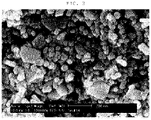
- Shapes of the synthesized core-shell nanoparticles are shown in FIGS. 3 and 4 , and the crystal phase is shown in FIG. 5 .
- Oleylamine (0.188 mol), oleic acid (0.0135 mol), copper acetate (0.014 mol), and nickel (II) acetylacetonate (0.019 mol) were mixed in a nitrogen atmosphere, and heated to 220°C. Then phenylhydrazine (0.261 mol) as a reducing agent was injected to prepare a reaction solution. The reaction solution was reacted for 60 minutes, and cooled to room temperature. Then, particles were extracted by centrifugation, and washed with toluene to synthesize nickel nanoparticles having an average size of 40 nm.
- Octylamine (1.410 mol), oleic acid (0.200 mol) and copper II acetate (0.140 mol) were mixed in a nitrogen atmosphere, and heated to 150°C. Then, phenylhydrazine (1.960 mol) as a reducing agent was injected to prepare a first reaction solution. The first reaction solution was reacted for 5 minutes, and cooled to room temperature. Then, particles were extracted by centrifugation, and washed with toluene, and the copper nanoparticles were analyzed by a transmission electron microscope. As a result, it was confirmed that a capping layer having a thickness of about 1 nm was formed on a copper core of a monocrystal.
- the capping layer was formed by oleic acid having an alkyl chain (C-C) and a carboxylate (-COO - ) moiety.
- the synthesized copper nanoparticles (2.41 g) (0.038 mol) were dispersed in 143.68 g of toluene, and 4.881 g (0.019 mol) of nickel(II) acetylacetonate and 4.237 g (0.015 mol) of oleic acid were mixed in a nitrogen atmosphere and heated to 240°C. Then, 29.097g (0.269 mol) of phenylhydrazine as a reducing agent was injected to prepare a second solution. After completion of the reaction for 1 hour, a second solution and chloroform were mixed in a volume ratio of 1 : 1.
- the copper core-nickel shell nanostructure was collected by centrifugation, and the particles were washed with a mixed solvent in which toluene and chloroform are mixed at a volume ratio of 1 : 1.
- a scanning electron microscope image of the obtained copper core-nickel shell nanoparticles is shown in FIG. 6A.
- FIG. 6A A scanning electron microscope image of the obtained copper core-nickel shell nanoparticles.
- the copper nanoparticles produced in Production Example 1 and the core-shell nanoparticles produced in Production Example 2 were mixed to produce mixed nanoparticles so that a weight ratio of Cu and Sn 3 Cu 10 was 95 : 5.
- the mixed nanoparticles (0.7 g) and BYK130 (7 mg) as a polymer binder material were mixed with 99.3 g of toluene, and spray-coated to form a coating film on a polyimide substrate heated to 80°C.
- Example 2 All processes were performed in the same manner as in Example 1 except that the copper nanoparticles produced in Production Example 1, the core-shell nanoparticles produced in Production Example 2, and the nickel nanoparticles produced in Production Example 3 were mixed to produce mixed nanoparticles so that a weight ratio of Cu : Sn 3 Cu 10 : Ni is 66.5:3.5:30, and the conditions for photonic sintering were changed.
- a conductive thin film having a thickness of 400 nm was produced by irradiating light under conditions of [1.5 msec, 2.0 kV, 1.22 J/cm 2 ], and the produced conductive thin film had specific resistance of 51.7 ⁇ cm.
- a change in resistance according to a storage time under high temperature and high humidity condition of 85%/85C was analyzed, and shown in FIG. 9 .
- the copper core-nickel shell nanoparticles (0.7 g) synthesized in Production Example 4 and BYK130 (7 mg) as a polymer binder material were mixed with 99.3 g of toluene and spray-coated to form a coating film on a polyimide substrate heated to 80° C.
- the specific resistance of the conductive metal thin film produced in Example 3 was measured, and as a result, it could be confirmed that when the irradiated light quantity was more than 2.6 J/cm 2 , the thin film partially peeled off or the thin film completely peeled off.
- the conductive metal thin film was analyzed by X-ray photoelectron spectroscopy (XPS) to measure the content of the polymer binder remained in the metal thin film for each light quantity of the irradiated light, and as a result, it was confirmed that in the metal thin films produced by irradiation with light quantity of more than 2.6 J/cm 2 in Examples, all of the polymer binders were substantially carbonized.
- XPS X-ray photoelectron spectroscopy
- Example 3 All processes were performed in the same manner as in Example 3 except that the copper core-nickel shell nanostructure synthesized in Production Example 5 was used.
- Example 3 All processes were performed in the same manner as in Example 3 except that the copper core-nickel shell nanostructure synthesized in Production Example 6 was used.
Landscapes
- Chemical & Material Sciences (AREA)
- Engineering & Computer Science (AREA)
- Life Sciences & Earth Sciences (AREA)
- Organic Chemistry (AREA)
- Wood Science & Technology (AREA)
- Materials Engineering (AREA)
- Dispersion Chemistry (AREA)
- Manufacturing & Machinery (AREA)
- Spectroscopy & Molecular Physics (AREA)
- Physics & Mathematics (AREA)
- Inorganic Chemistry (AREA)
- Conductive Materials (AREA)
- Inks, Pencil-Leads, Or Crayons (AREA)
- Powder Metallurgy (AREA)
Claims (10)
- Composition d'encre destinée au frittage photonique, la composition comprenant :une première nanoparticule métallique comprenant un premier métal, la première nanoparticule métallique étant recouverte d'une première couche de recouvrement comprenant un acide organique, la première couche de recouvrement empêchant sensiblement complètement la formation d'un film d'oxyde de surface par le premier métal ;une particule en métal à point de fusion bas, recouverte d'une troisième couche de recouvrement comprenant un acide organique empêchant sensiblement complètement la formation d'un film d'oxyde de surface, le métal à point de fusion bas présentant un point de fusion égal ou inférieur à 800 °C ;un liant organique non aqueux ; etun solvant non aqueux,le premier métal étant du cuivre, de l'argent, de l'or, du nickel, de l'étain, de l'aluminium ou un alliage desdits métaux.
- La composition d'encre destinée au frittage photonique de la revendication 1, dans laquelle le métal à point de fusion bas est un alliage composé de deux ou plusieurs métaux choisis parmi le cuivre, l'étain, l'argent, le bismuth, le zinc, l'indium et le plomb.
- La composition d'encre destinée au frittage photonique de la revendication 2, dans laquelle le métal à point de fusion bas est un alliage à base de cuivre-étain.
- La composition d'encre destinée au frittage photonique de la revendication 3, dans laquelle l'alliage à base de cuivre-étain satisfait à la Formule Chimique 1 suivante :
[Formule Chimique 1] Cu1Snx
et dans la Formule Chimique 1, x est 0,1 ≤ x ≤ 2. - Composition d'encre destinée au frittage photonique, la composition comprenant :une première nanoparticule métallique comprenant un premier métal, la première nanoparticule métallique étant une nanostructure noyau-coque comprenant le premier métal en tant que noyau, le premier métal empêchant sensiblement complètement la formation d'un film d'oxyde de surface ; une coque en un deuxième métal entourant le noyau ; et une deuxième couche de recouvrement entourant la coque en deuxième métal ;une particule en métal à point de fusion bas, recouverte d'une troisième couche de recouvrement comprenant un acide organique empêchant sensiblement complètement la formation d'un film d'oxyde de surface, le métal à point de fusion bas présentant un point de fusion égal ou inférieur à 800 °C ;un liant organique non aqueux ; etun solvant non aqueux,le premier métal étant du cuivre, de l'argent, de l'or, du nickel, de l'étain, de l'aluminium ou un alliage de ceux-ci.
- La composition d'encre destinée au frittage photonique de la revendication 5, dans laquelle le deuxième métal est du cuivre, de l'argent, de l'or, du nickel, de l'étain, de l'aluminium ou un alliage desdits métaux, et le premier métal et le deuxième métal sont différents l'un de l'autre.
- La composition d'encre destinée au frittage photonique de la revendication 5, dans laquelle la deuxième couche de recouvrement contient un acide organique.
- Procédé de préparation d'une composition d'encre destinée au frittage photonique selon la revendication 1, le procédé comprenant :a) la synthèse d'une première nanoparticule métallique comprenant un premier métal, la première nanoparticule métallique étant recouverte d'une première couche de recouvrement comprenant un acide organique, la première couche de recouvrement empêchant sensiblement complètement la formation d'un film d'oxyde de surface par le premier métal, au moyen du chauffage et de l'agitation d'une solution de réaction comprenant un précurseur métallique, l'acide organique, un composé à base d'aminé et un agent réducteur ; etb) la préparation d'une dispersion dans laquelle la première nanoparticule métallique, une particule en métal à point de fusion bas recouverte d'une troisième couche de recouvrement comprenant un acide organique, le métal à point de fusion bas présentant un point de fusion égal ou inférieur à 800 °C et la troisième couche de recouvrement empêchant sensiblement complètement la formation d'un film d'oxyde de surface, et un liant organique non aqueux, sont dispersés dans un solvant non aqueux,le premier métal étant du cuivre, de l'argent, de l'or, du nickel, de l'étain, de l'aluminium ou un alliage desdits métaux.
- Procédé de préparation d'une composition d'encre destinée au frittage photonique selon la revendication 5, le procédé comprenant :a) la synthèse d'une première nanoparticule métallique comprenant un premier métal, ladite synthèse comprenant les sous-étapes suivantes :a-1) la synthèse d'un noyau en premier métal comprenant le premier métal, le noyau en premier métal étant recouvert d'une première couche de recouvrement empêchant sensiblement complètement la formation d'un film d'oxyde de surface, au moyen du chauffage et de l'agitation d'une première solution comprenant un premier précurseur métallique, un premier acide organique, un premier composé à base d'aminé et un premier agent réducteur ; eta-2) la synthèse d'une nanostructure noyau-coque présentant une structure dans laquelle le noyau en premier métal, une coque en un deuxième métal et une deuxième couche de recouvrement sont positionnés successivement de l'intérieur vers l'extérieur, au moyen du chauffage et de l'agitation du noyau en premier métal, et d'une deuxième solution comprenant un deuxième précurseur métallique, un deuxième acide organique, un deuxième composé à base d'aminé et un deuxième agent réducteur,etb) la préparation d'une dispersion dans laquelle la première nanoparticule métallique, une particule en métal à point de fusion bas recouverte d'une troisième couche de recouvrement comprenant un acide organique, le métal à point de fusion bas présentant un point de fusion égal ou inférieur à 800 °C et la troisième couche de recouvrement empêchant sensiblement complètement la formation d'un film d'oxyde de surface, et un liant organique non aqueux, sont dispersés dans un solvant non aqueux,le premier métal étant du cuivre, de l'argent, de l'or, du nickel, de l'étain, de l'aluminium ou un alliage desdits métaux.
- Procédé de production d'un film mince conducteur de frittage photonique, le procédé comprenant :A) la préparation d'une composition d'encre destinée au frittage photonique selon l'une quelconque des revendication 1 à 7 ;B) l'application de la composition d'encre destinée au frittage photonique sur un substrat afin de former un film de revêtement ; etC) l'irradiation du film de revêtement à l'aide d'une lumière visible présentant une énergie égale ou inférieure à 1,3 J/cm2 dans une bande de longueur d'onde comprise entre 400 et 800 nm, afin de produire un film mince conducteur.
Applications Claiming Priority (3)
| Application Number | Priority Date | Filing Date | Title |
|---|---|---|---|
| KR1020150148667A KR20170047936A (ko) | 2015-10-26 | 2015-10-26 | 광소결용 잉크조성물 및 이의 제조방법 |
| KR1020150149140A KR101802194B1 (ko) | 2015-10-27 | 2015-10-27 | 광소결용 잉크조성물 및 이의 제조방법 |
| PCT/KR2016/011824 WO2017073956A1 (fr) | 2015-10-26 | 2016-10-20 | Composition d'encre pour frittage photonique et son procédé de production |
Publications (3)
| Publication Number | Publication Date |
|---|---|
| EP3354698A1 EP3354698A1 (fr) | 2018-08-01 |
| EP3354698A4 EP3354698A4 (fr) | 2019-05-15 |
| EP3354698B1 true EP3354698B1 (fr) | 2022-09-21 |
Family
ID=58630984
Family Applications (1)
| Application Number | Title | Priority Date | Filing Date |
|---|---|---|---|
| EP16860139.1A Active EP3354698B1 (fr) | 2015-10-26 | 2016-10-20 | Composition d'encre pour frittage photonique et son procédé de production |
Country Status (4)
| Country | Link |
|---|---|
| US (1) | US10822511B2 (fr) |
| EP (1) | EP3354698B1 (fr) |
| CN (2) | CN121379248A (fr) |
| WO (1) | WO2017073956A1 (fr) |
Families Citing this family (4)
| Publication number | Priority date | Publication date | Assignee | Title |
|---|---|---|---|---|
| US10120111B2 (en) * | 2016-12-14 | 2018-11-06 | Google Llc | Thin ceramic imaging screen for camera systems |
| US20200095442A1 (en) * | 2017-06-05 | 2020-03-26 | Nano Dimensions Technologies Ltd. | Flocculates of metallic, geometrically discrete nanoparticles compositions and methods of forming the same |
| CN113956721B (zh) * | 2021-11-29 | 2023-02-03 | 陕西工业职业技术学院 | 一种采用光子烧结技术制备Cu/Cu6Sn5导电油墨的方法 |
| CN115171945A (zh) * | 2022-05-31 | 2022-10-11 | 宁波柔印电子科技有限责任公司 | 一种可用于大面积制备的铜浆及制作方法 |
Family Cites Families (13)
| Publication number | Priority date | Publication date | Assignee | Title |
|---|---|---|---|---|
| KR100836659B1 (ko) * | 2006-07-06 | 2008-06-10 | 삼성전기주식회사 | 금속 및 금속 산화물 나노입자의 제조방법 |
| US20090181172A1 (en) * | 2007-10-15 | 2009-07-16 | Nanoink, Inc. | Lithography of nanoparticle based inks |
| US7749300B2 (en) | 2008-06-05 | 2010-07-06 | Xerox Corporation | Photochemical synthesis of bimetallic core-shell nanoparticles |
| KR101418276B1 (ko) * | 2012-03-30 | 2014-07-15 | 한국화학연구원 | 표면 산화막 형성이 제어된 금속 나노 입자 합성 방법 및 용액 공정을 통한 금속 전도성 박막의 제조방법 |
| US9205410B2 (en) * | 2012-04-03 | 2015-12-08 | University Of South Carolina | One-step synthesis of monodisperse transition metal core-shell nanoparticles with solid solution shells |
| KR20140027624A (ko) * | 2012-08-23 | 2014-03-07 | 삼성정밀화학 주식회사 | 상전이 환원법을 이용한 금속 나노입자의 제조방법 및 이로부터 제조된 금속 나노입자를 포함한 금속잉크 |
| KR20140094690A (ko) * | 2013-01-21 | 2014-07-31 | 엘에스전선 주식회사 | 전도성 잉크 조성물 및 이로부터 전극을 형성하는 방법 |
| FI20135253L (fi) * | 2013-03-15 | 2014-09-16 | Inkron Ltd | Monikerrosmetallipartikkelit ja niiden käyttö |
| JP6194108B2 (ja) * | 2013-08-01 | 2017-09-06 | エルジー・ケム・リミテッド | 太陽電池の光吸収層製造用インク組成物及びこれを使用した薄膜の製造方法 |
| US20150189761A1 (en) * | 2013-12-20 | 2015-07-02 | Intrinsiq Materials, Inc. | Method for depositing and curing nanoparticle-based ink |
| KR101947633B1 (ko) * | 2014-04-15 | 2019-02-14 | (주)쎄미시스코 | 전도성 구리 복합잉크 및 이를 이용한 광소결 방법 |
| US10563080B2 (en) * | 2014-08-29 | 2020-02-18 | University Of Louisville Research Foundation, Inc. | Core-shell nanostructures and related inks, films and methods |
| CN104810115B (zh) * | 2015-04-03 | 2018-03-16 | 清华大学深圳研究生院 | 一种导电膜、导电膜的制备方法及其使用的油墨 |
-
2016
- 2016-10-20 WO PCT/KR2016/011824 patent/WO2017073956A1/fr not_active Ceased
- 2016-10-20 CN CN202511376308.0A patent/CN121379248A/zh active Pending
- 2016-10-20 US US15/770,995 patent/US10822511B2/en active Active
- 2016-10-20 CN CN201680062322.6A patent/CN108350300A/zh active Pending
- 2016-10-20 EP EP16860139.1A patent/EP3354698B1/fr active Active
Also Published As
| Publication number | Publication date |
|---|---|
| EP3354698A4 (fr) | 2019-05-15 |
| WO2017073956A1 (fr) | 2017-05-04 |
| CN108350300A (zh) | 2018-07-31 |
| CN121379248A (zh) | 2026-01-23 |
| US10822511B2 (en) | 2020-11-03 |
| US20180312709A1 (en) | 2018-11-01 |
| EP3354698A1 (fr) | 2018-08-01 |
Similar Documents
| Publication | Publication Date | Title |
|---|---|---|
| EP2785158B1 (fr) | Procédé de formation de motifs conducteurs et composition pour former un motif conducteur par exposition à une lumière ou chauffage par micro-ondes | |
| EP3354698B1 (fr) | Composition d'encre pour frittage photonique et son procédé de production | |
| CN102119065B (zh) | 铜系纳米粒子及其制造方法 | |
| US20120251736A1 (en) | Conductive ink composition, method for manufacturing the same, and method for manufacturing conductive thin layer using the same | |
| KR101785350B1 (ko) | 광소결을 이용한 전도성 금속박막의 제조방법 | |
| KR20170139649A (ko) | 분산체 | |
| TWI661012B (zh) | 核殼型金屬微粒子之製造方法、核殼型金屬微粒子、導電性墨水及基板之製造方法 | |
| KR20150082133A (ko) | 전도성 하이브리드 구리잉크 및 이를 이용한 광소결 방법 | |
| CN106413951A (zh) | 金属纳米颗粒及其制备方法 | |
| KR101909435B1 (ko) | 광소결용 잉크조성물 및 이의 제조방법 | |
| Yuan et al. | Submicron Cu@ glass core-shell powders for the preparation of conductive thick films on ceramic substrates | |
| Yonezawa et al. | Particle size tuning in scalable synthesis of anti-oxidized copper fine particles by polypeptide molecular weights | |
| KR101802194B1 (ko) | 광소결용 잉크조성물 및 이의 제조방법 | |
| KR20170047936A (ko) | 광소결용 잉크조성물 및 이의 제조방법 | |
| KR101935273B1 (ko) | 구리 나노입자 및 이의 제조방법 | |
| JP2016145397A (ja) | 銅膜の製造方法及びそれにより得られた導電体 | |
| KR101798277B1 (ko) | 판상형 산화구리 나노물질을 이용한 전도성 구리박막 패턴의 제조방법 | |
| Lee et al. | Preparation of size-controlled fine Al particles for application to rear electrode of Si solar cells | |
| Zhang et al. | A simple way to prepare large-scale copper nanoparticles for conductive ink in printed electronics | |
| JP5124822B2 (ja) | 複合金属粉体およびその分散液の製造法 | |
| WO2013147535A1 (fr) | Procédé de synthèse pour empêcher des nanoparticules métalliques de présenter un film oxydé et procédé de fabrication d'un film mince métallique conducteur par un traitement en solution | |
| JP7663768B1 (ja) | 導電膜及びその形成方法 | |
| KR102201875B1 (ko) | 광소결용 내열 합금 조성물 및 이를 이용한 전도성 내열 합금막의 제조방법 | |
| Ghule et al. | Synthesis and Characterization of Silver‐Nanoparticle‐Deposited α‐Bi2Mo3O12 Nanorods | |
| Mainak et al. | Metal-based conducive nano-inks: A review of synthesis and characterisation techniques |
Legal Events
| Date | Code | Title | Description |
|---|---|---|---|
| STAA | Information on the status of an ep patent application or granted ep patent |
Free format text: STATUS: THE INTERNATIONAL PUBLICATION HAS BEEN MADE |
|
| PUAI | Public reference made under article 153(3) epc to a published international application that has entered the european phase |
Free format text: ORIGINAL CODE: 0009012 |
|
| STAA | Information on the status of an ep patent application or granted ep patent |
Free format text: STATUS: REQUEST FOR EXAMINATION WAS MADE |
|
| 17P | Request for examination filed |
Effective date: 20180425 |
|
| AK | Designated contracting states |
Kind code of ref document: A1 Designated state(s): AL AT BE BG CH CY CZ DE DK EE ES FI FR GB GR HR HU IE IS IT LI LT LU LV MC MK MT NL NO PL PT RO RS SE SI SK SM TR |
|
| AX | Request for extension of the european patent |
Extension state: BA ME |
|
| DAV | Request for validation of the european patent (deleted) | ||
| DAX | Request for extension of the european patent (deleted) | ||
| A4 | Supplementary search report drawn up and despatched |
Effective date: 20190411 |
|
| RIC1 | Information provided on ipc code assigned before grant |
Ipc: C09D 11/52 20140101AFI20190405BHEP Ipc: C09D 5/24 20060101ALI20190405BHEP Ipc: H01B 13/00 20060101ALI20190405BHEP Ipc: H01B 1/22 20060101ALI20190405BHEP |
|
| STAA | Information on the status of an ep patent application or granted ep patent |
Free format text: STATUS: EXAMINATION IS IN PROGRESS |
|
| 17Q | First examination report despatched |
Effective date: 20200107 |
|
| GRAP | Despatch of communication of intention to grant a patent |
Free format text: ORIGINAL CODE: EPIDOSNIGR1 |
|
| STAA | Information on the status of an ep patent application or granted ep patent |
Free format text: STATUS: GRANT OF PATENT IS INTENDED |
|
| INTG | Intention to grant announced |
Effective date: 20220421 |
|
| GRAS | Grant fee paid |
Free format text: ORIGINAL CODE: EPIDOSNIGR3 |
|
| GRAA | (expected) grant |
Free format text: ORIGINAL CODE: 0009210 |
|
| STAA | Information on the status of an ep patent application or granted ep patent |
Free format text: STATUS: THE PATENT HAS BEEN GRANTED |
|
| AK | Designated contracting states |
Kind code of ref document: B1 Designated state(s): AL AT BE BG CH CY CZ DE DK EE ES FI FR GB GR HR HU IE IS IT LI LT LU LV MC MK MT NL NO PL PT RO RS SE SI SK SM TR |
|
| REG | Reference to a national code |
Ref country code: GB Ref legal event code: FG4D |
|
| REG | Reference to a national code |
Ref country code: CH Ref legal event code: EP |
|
| REG | Reference to a national code |
Ref country code: IE Ref legal event code: FG4D |
|
| REG | Reference to a national code |
Ref country code: DE Ref legal event code: R096 Ref document number: 602016075193 Country of ref document: DE |
|
| REG | Reference to a national code |
Ref country code: AT Ref legal event code: REF Ref document number: 1519950 Country of ref document: AT Kind code of ref document: T Effective date: 20221015 |
|
| REG | Reference to a national code |
Ref country code: LT Ref legal event code: MG9D |
|
| REG | Reference to a national code |
Ref country code: NL Ref legal event code: MP Effective date: 20220921 |
|
| PG25 | Lapsed in a contracting state [announced via postgrant information from national office to epo] |
Ref country code: SE Free format text: LAPSE BECAUSE OF FAILURE TO SUBMIT A TRANSLATION OF THE DESCRIPTION OR TO PAY THE FEE WITHIN THE PRESCRIBED TIME-LIMIT Effective date: 20220921 Ref country code: RS Free format text: LAPSE BECAUSE OF FAILURE TO SUBMIT A TRANSLATION OF THE DESCRIPTION OR TO PAY THE FEE WITHIN THE PRESCRIBED TIME-LIMIT Effective date: 20220921 Ref country code: NO Free format text: LAPSE BECAUSE OF FAILURE TO SUBMIT A TRANSLATION OF THE DESCRIPTION OR TO PAY THE FEE WITHIN THE PRESCRIBED TIME-LIMIT Effective date: 20221221 Ref country code: LV Free format text: LAPSE BECAUSE OF FAILURE TO SUBMIT A TRANSLATION OF THE DESCRIPTION OR TO PAY THE FEE WITHIN THE PRESCRIBED TIME-LIMIT Effective date: 20220921 Ref country code: LT Free format text: LAPSE BECAUSE OF FAILURE TO SUBMIT A TRANSLATION OF THE DESCRIPTION OR TO PAY THE FEE WITHIN THE PRESCRIBED TIME-LIMIT Effective date: 20220921 Ref country code: FI Free format text: LAPSE BECAUSE OF FAILURE TO SUBMIT A TRANSLATION OF THE DESCRIPTION OR TO PAY THE FEE WITHIN THE PRESCRIBED TIME-LIMIT Effective date: 20220921 |
|
| REG | Reference to a national code |
Ref country code: AT Ref legal event code: MK05 Ref document number: 1519950 Country of ref document: AT Kind code of ref document: T Effective date: 20220921 |
|
| PG25 | Lapsed in a contracting state [announced via postgrant information from national office to epo] |
Ref country code: HR Free format text: LAPSE BECAUSE OF FAILURE TO SUBMIT A TRANSLATION OF THE DESCRIPTION OR TO PAY THE FEE WITHIN THE PRESCRIBED TIME-LIMIT Effective date: 20220921 Ref country code: GR Free format text: LAPSE BECAUSE OF FAILURE TO SUBMIT A TRANSLATION OF THE DESCRIPTION OR TO PAY THE FEE WITHIN THE PRESCRIBED TIME-LIMIT Effective date: 20221222 |
|
| PG25 | Lapsed in a contracting state [announced via postgrant information from national office to epo] |
Ref country code: SM Free format text: LAPSE BECAUSE OF FAILURE TO SUBMIT A TRANSLATION OF THE DESCRIPTION OR TO PAY THE FEE WITHIN THE PRESCRIBED TIME-LIMIT Effective date: 20220921 Ref country code: RO Free format text: LAPSE BECAUSE OF FAILURE TO SUBMIT A TRANSLATION OF THE DESCRIPTION OR TO PAY THE FEE WITHIN THE PRESCRIBED TIME-LIMIT Effective date: 20220921 Ref country code: PT Free format text: LAPSE BECAUSE OF FAILURE TO SUBMIT A TRANSLATION OF THE DESCRIPTION OR TO PAY THE FEE WITHIN THE PRESCRIBED TIME-LIMIT Effective date: 20230123 Ref country code: ES Free format text: LAPSE BECAUSE OF FAILURE TO SUBMIT A TRANSLATION OF THE DESCRIPTION OR TO PAY THE FEE WITHIN THE PRESCRIBED TIME-LIMIT Effective date: 20220921 Ref country code: CZ Free format text: LAPSE BECAUSE OF FAILURE TO SUBMIT A TRANSLATION OF THE DESCRIPTION OR TO PAY THE FEE WITHIN THE PRESCRIBED TIME-LIMIT Effective date: 20220921 Ref country code: AT Free format text: LAPSE BECAUSE OF FAILURE TO SUBMIT A TRANSLATION OF THE DESCRIPTION OR TO PAY THE FEE WITHIN THE PRESCRIBED TIME-LIMIT Effective date: 20220921 |
|
| PG25 | Lapsed in a contracting state [announced via postgrant information from national office to epo] |
Ref country code: SK Free format text: LAPSE BECAUSE OF FAILURE TO SUBMIT A TRANSLATION OF THE DESCRIPTION OR TO PAY THE FEE WITHIN THE PRESCRIBED TIME-LIMIT Effective date: 20220921 Ref country code: PL Free format text: LAPSE BECAUSE OF FAILURE TO SUBMIT A TRANSLATION OF THE DESCRIPTION OR TO PAY THE FEE WITHIN THE PRESCRIBED TIME-LIMIT Effective date: 20220921 Ref country code: IS Free format text: LAPSE BECAUSE OF FAILURE TO SUBMIT A TRANSLATION OF THE DESCRIPTION OR TO PAY THE FEE WITHIN THE PRESCRIBED TIME-LIMIT Effective date: 20230121 Ref country code: EE Free format text: LAPSE BECAUSE OF FAILURE TO SUBMIT A TRANSLATION OF THE DESCRIPTION OR TO PAY THE FEE WITHIN THE PRESCRIBED TIME-LIMIT Effective date: 20220921 |
|
| REG | Reference to a national code |
Ref country code: CH Ref legal event code: PL |
|
| REG | Reference to a national code |
Ref country code: DE Ref legal event code: R097 Ref document number: 602016075193 Country of ref document: DE |
|
| REG | Reference to a national code |
Ref country code: BE Ref legal event code: MM Effective date: 20221031 |
|
| P01 | Opt-out of the competence of the unified patent court (upc) registered |
Effective date: 20230524 |
|
| PG25 | Lapsed in a contracting state [announced via postgrant information from national office to epo] |
Ref country code: NL Free format text: LAPSE BECAUSE OF FAILURE TO SUBMIT A TRANSLATION OF THE DESCRIPTION OR TO PAY THE FEE WITHIN THE PRESCRIBED TIME-LIMIT Effective date: 20220921 Ref country code: MC Free format text: LAPSE BECAUSE OF FAILURE TO SUBMIT A TRANSLATION OF THE DESCRIPTION OR TO PAY THE FEE WITHIN THE PRESCRIBED TIME-LIMIT Effective date: 20220921 Ref country code: LU Free format text: LAPSE BECAUSE OF NON-PAYMENT OF DUE FEES Effective date: 20221020 Ref country code: AL Free format text: LAPSE BECAUSE OF FAILURE TO SUBMIT A TRANSLATION OF THE DESCRIPTION OR TO PAY THE FEE WITHIN THE PRESCRIBED TIME-LIMIT Effective date: 20220921 |
|
| PLBE | No opposition filed within time limit |
Free format text: ORIGINAL CODE: 0009261 |
|
| STAA | Information on the status of an ep patent application or granted ep patent |
Free format text: STATUS: NO OPPOSITION FILED WITHIN TIME LIMIT |
|
| PG25 | Lapsed in a contracting state [announced via postgrant information from national office to epo] |
Ref country code: LI Free format text: LAPSE BECAUSE OF NON-PAYMENT OF DUE FEES Effective date: 20221031 Ref country code: DK Free format text: LAPSE BECAUSE OF FAILURE TO SUBMIT A TRANSLATION OF THE DESCRIPTION OR TO PAY THE FEE WITHIN THE PRESCRIBED TIME-LIMIT Effective date: 20220921 Ref country code: CH Free format text: LAPSE BECAUSE OF NON-PAYMENT OF DUE FEES Effective date: 20221031 |
|
| 26N | No opposition filed |
Effective date: 20230622 |
|
| PG25 | Lapsed in a contracting state [announced via postgrant information from national office to epo] |
Ref country code: SI Free format text: LAPSE BECAUSE OF FAILURE TO SUBMIT A TRANSLATION OF THE DESCRIPTION OR TO PAY THE FEE WITHIN THE PRESCRIBED TIME-LIMIT Effective date: 20220921 |
|
| PG25 | Lapsed in a contracting state [announced via postgrant information from national office to epo] |
Ref country code: BE Free format text: LAPSE BECAUSE OF NON-PAYMENT OF DUE FEES Effective date: 20221031 |
|
| PG25 | Lapsed in a contracting state [announced via postgrant information from national office to epo] |
Ref country code: IE Free format text: LAPSE BECAUSE OF NON-PAYMENT OF DUE FEES Effective date: 20221020 |
|
| PG25 | Lapsed in a contracting state [announced via postgrant information from national office to epo] |
Ref country code: FR Free format text: LAPSE BECAUSE OF NON-PAYMENT OF DUE FEES Effective date: 20221121 |
|
| PG25 | Lapsed in a contracting state [announced via postgrant information from national office to epo] |
Ref country code: HU Free format text: LAPSE BECAUSE OF FAILURE TO SUBMIT A TRANSLATION OF THE DESCRIPTION OR TO PAY THE FEE WITHIN THE PRESCRIBED TIME-LIMIT; INVALID AB INITIO Effective date: 20161020 |
|
| PG25 | Lapsed in a contracting state [announced via postgrant information from national office to epo] |
Ref country code: CY Free format text: LAPSE BECAUSE OF FAILURE TO SUBMIT A TRANSLATION OF THE DESCRIPTION OR TO PAY THE FEE WITHIN THE PRESCRIBED TIME-LIMIT Effective date: 20220921 |
|
| PG25 | Lapsed in a contracting state [announced via postgrant information from national office to epo] |
Ref country code: MK Free format text: LAPSE BECAUSE OF FAILURE TO SUBMIT A TRANSLATION OF THE DESCRIPTION OR TO PAY THE FEE WITHIN THE PRESCRIBED TIME-LIMIT Effective date: 20220921 Ref country code: IT Free format text: LAPSE BECAUSE OF FAILURE TO SUBMIT A TRANSLATION OF THE DESCRIPTION OR TO PAY THE FEE WITHIN THE PRESCRIBED TIME-LIMIT Effective date: 20220921 |
|
| PG25 | Lapsed in a contracting state [announced via postgrant information from national office to epo] |
Ref country code: TR Free format text: LAPSE BECAUSE OF FAILURE TO SUBMIT A TRANSLATION OF THE DESCRIPTION OR TO PAY THE FEE WITHIN THE PRESCRIBED TIME-LIMIT Effective date: 20220921 |
|
| PG25 | Lapsed in a contracting state [announced via postgrant information from national office to epo] |
Ref country code: BG Free format text: LAPSE BECAUSE OF FAILURE TO SUBMIT A TRANSLATION OF THE DESCRIPTION OR TO PAY THE FEE WITHIN THE PRESCRIBED TIME-LIMIT Effective date: 20220921 |
|
| PG25 | Lapsed in a contracting state [announced via postgrant information from national office to epo] |
Ref country code: MT Free format text: LAPSE BECAUSE OF FAILURE TO SUBMIT A TRANSLATION OF THE DESCRIPTION OR TO PAY THE FEE WITHIN THE PRESCRIBED TIME-LIMIT Effective date: 20220921 |
|
| PGFP | Annual fee paid to national office [announced via postgrant information from national office to epo] |
Ref country code: GB Payment date: 20250922 Year of fee payment: 10 |
|
| PGFP | Annual fee paid to national office [announced via postgrant information from national office to epo] |
Ref country code: DE Payment date: 20250922 Year of fee payment: 10 |