EP3355342A1 - Laserunterstützte lötverbindung eines direktumwandlungsverbindungshalbleiterdetektors - Google Patents
Laserunterstützte lötverbindung eines direktumwandlungsverbindungshalbleiterdetektors Download PDFInfo
- Publication number
- EP3355342A1 EP3355342A1 EP17153476.1A EP17153476A EP3355342A1 EP 3355342 A1 EP3355342 A1 EP 3355342A1 EP 17153476 A EP17153476 A EP 17153476A EP 3355342 A1 EP3355342 A1 EP 3355342A1
- Authority
- EP
- European Patent Office
- Prior art keywords
- readout
- compound semiconductor
- direct conversion
- semiconductor sensor
- conversion compound
- Prior art date
- Legal status (The legal status is an assumption and is not a legal conclusion. Google has not performed a legal analysis and makes no representation as to the accuracy of the status listed.)
- Withdrawn
Links
Images


Classifications
-
- B—PERFORMING OPERATIONS; TRANSPORTING
- B23—MACHINE TOOLS; METAL-WORKING NOT OTHERWISE PROVIDED FOR
- B23K—SOLDERING OR UNSOLDERING; WELDING; CLADDING OR PLATING BY SOLDERING OR WELDING; CUTTING BY APPLYING HEAT LOCALLY, e.g. FLAME CUTTING; WORKING BY LASER BEAM
- B23K1/00—Soldering, e.g. brazing, or unsoldering
- B23K1/005—Soldering by means of radiant energy
- B23K1/0056—Soldering by means of radiant energy soldering by means of beams, e.g. lasers, electron beams [EB]
-
- H—ELECTRICITY
- H10—SEMICONDUCTOR DEVICES; ELECTRIC SOLID-STATE DEVICES NOT OTHERWISE PROVIDED FOR
- H10F—INORGANIC SEMICONDUCTOR DEVICES SENSITIVE TO INFRARED RADIATION, LIGHT, ELECTROMAGNETIC RADIATION OF SHORTER WAVELENGTH OR CORPUSCULAR RADIATION
- H10F39/00—Integrated devices, or assemblies of multiple devices, comprising at least one element covered by group H10F30/00, e.g. radiation detectors comprising photodiode arrays
- H10F39/80—Constructional details of image sensors
- H10F39/811—Interconnections
-
- H—ELECTRICITY
- H10—SEMICONDUCTOR DEVICES; ELECTRIC SOLID-STATE DEVICES NOT OTHERWISE PROVIDED FOR
- H10F—INORGANIC SEMICONDUCTOR DEVICES SENSITIVE TO INFRARED RADIATION, LIGHT, ELECTROMAGNETIC RADIATION OF SHORTER WAVELENGTH OR CORPUSCULAR RADIATION
- H10F39/00—Integrated devices, or assemblies of multiple devices, comprising at least one element covered by group H10F30/00, e.g. radiation detectors comprising photodiode arrays
- H10F39/011—Manufacture or treatment of image sensors covered by group H10F39/12
- H10F39/018—Manufacture or treatment of image sensors covered by group H10F39/12 of hybrid image sensors
-
- H—ELECTRICITY
- H10—SEMICONDUCTOR DEVICES; ELECTRIC SOLID-STATE DEVICES NOT OTHERWISE PROVIDED FOR
- H10F—INORGANIC SEMICONDUCTOR DEVICES SENSITIVE TO INFRARED RADIATION, LIGHT, ELECTROMAGNETIC RADIATION OF SHORTER WAVELENGTH OR CORPUSCULAR RADIATION
- H10F39/00—Integrated devices, or assemblies of multiple devices, comprising at least one element covered by group H10F30/00, e.g. radiation detectors comprising photodiode arrays
- H10F39/10—Integrated devices
- H10F39/12—Image sensors
- H10F39/18—Complementary metal-oxide-semiconductor [CMOS] image sensors; Photodiode array image sensors
- H10F39/189—X-ray, gamma-ray or corpuscular radiation imagers
- H10F39/1895—X-ray, gamma-ray or corpuscular radiation imagers of the hybrid type
-
- H—ELECTRICITY
- H10—SEMICONDUCTOR DEVICES; ELECTRIC SOLID-STATE DEVICES NOT OTHERWISE PROVIDED FOR
- H10W—GENERIC PACKAGES, INTERCONNECTIONS, CONNECTORS OR OTHER CONSTRUCTIONAL DETAILS OF DEVICES COVERED BY CLASS H10
- H10W72/00—Interconnections or connectors in packages
- H10W72/01—Manufacture or treatment
- H10W72/012—Manufacture or treatment of bump connectors, dummy bumps or thermal bumps
-
- H—ELECTRICITY
- H05—ELECTRIC TECHNIQUES NOT OTHERWISE PROVIDED FOR
- H05K—PRINTED CIRCUITS; CASINGS OR CONSTRUCTIONAL DETAILS OF ELECTRIC APPARATUS; MANUFACTURE OF ASSEMBLAGES OF ELECTRICAL COMPONENTS
- H05K2201/00—Indexing scheme relating to printed circuits covered by H05K1/00
- H05K2201/10—Details of components or other objects attached to or integrated in a printed circuit board
- H05K2201/10613—Details of electrical connections of non-printed components, e.g. special leads
- H05K2201/10621—Components characterised by their electrical contacts
- H05K2201/10734—Ball grid array [BGA]; Bump grid array
-
- H—ELECTRICITY
- H10—SEMICONDUCTOR DEVICES; ELECTRIC SOLID-STATE DEVICES NOT OTHERWISE PROVIDED FOR
- H10W—GENERIC PACKAGES, INTERCONNECTIONS, CONNECTORS OR OTHER CONSTRUCTIONAL DETAILS OF DEVICES COVERED BY CLASS H10
- H10W72/00—Interconnections or connectors in packages
- H10W72/01—Manufacture or treatment
- H10W72/012—Manufacture or treatment of bump connectors, dummy bumps or thermal bumps
- H10W72/01221—Manufacture or treatment of bump connectors, dummy bumps or thermal bumps using local deposition
- H10W72/01223—Manufacture or treatment of bump connectors, dummy bumps or thermal bumps using local deposition in liquid form, e.g. by dispensing droplets or by screen printing
-
- H—ELECTRICITY
- H10—SEMICONDUCTOR DEVICES; ELECTRIC SOLID-STATE DEVICES NOT OTHERWISE PROVIDED FOR
- H10W—GENERIC PACKAGES, INTERCONNECTIONS, CONNECTORS OR OTHER CONSTRUCTIONAL DETAILS OF DEVICES COVERED BY CLASS H10
- H10W72/00—Interconnections or connectors in packages
- H10W72/071—Connecting or disconnecting
- H10W72/072—Connecting or disconnecting of bump connectors
- H10W72/07231—Techniques
- H10W72/07232—Compression bonding, e.g. thermocompression bonding
-
- H—ELECTRICITY
- H10—SEMICONDUCTOR DEVICES; ELECTRIC SOLID-STATE DEVICES NOT OTHERWISE PROVIDED FOR
- H10W—GENERIC PACKAGES, INTERCONNECTIONS, CONNECTORS OR OTHER CONSTRUCTIONAL DETAILS OF DEVICES COVERED BY CLASS H10
- H10W72/00—Interconnections or connectors in packages
- H10W72/071—Connecting or disconnecting
- H10W72/072—Connecting or disconnecting of bump connectors
- H10W72/07231—Techniques
- H10W72/07235—Applying EM radiation, e.g. induction heating or using a laser
-
- H—ELECTRICITY
- H10—SEMICONDUCTOR DEVICES; ELECTRIC SOLID-STATE DEVICES NOT OTHERWISE PROVIDED FOR
- H10W—GENERIC PACKAGES, INTERCONNECTIONS, CONNECTORS OR OTHER CONSTRUCTIONAL DETAILS OF DEVICES COVERED BY CLASS H10
- H10W72/00—Interconnections or connectors in packages
- H10W72/071—Connecting or disconnecting
- H10W72/072—Connecting or disconnecting of bump connectors
- H10W72/07231—Techniques
- H10W72/07236—Soldering or alloying
-
- H—ELECTRICITY
- H10—SEMICONDUCTOR DEVICES; ELECTRIC SOLID-STATE DEVICES NOT OTHERWISE PROVIDED FOR
- H10W—GENERIC PACKAGES, INTERCONNECTIONS, CONNECTORS OR OTHER CONSTRUCTIONAL DETAILS OF DEVICES COVERED BY CLASS H10
- H10W72/00—Interconnections or connectors in packages
- H10W72/20—Bump connectors, e.g. solder bumps or copper pillars; Dummy bumps; Thermal bumps
- H10W72/221—Structures or relative sizes
- H10W72/227—Multiple bumps having different sizes
-
- H—ELECTRICITY
- H10—SEMICONDUCTOR DEVICES; ELECTRIC SOLID-STATE DEVICES NOT OTHERWISE PROVIDED FOR
- H10W—GENERIC PACKAGES, INTERCONNECTIONS, CONNECTORS OR OTHER CONSTRUCTIONAL DETAILS OF DEVICES COVERED BY CLASS H10
- H10W72/00—Interconnections or connectors in packages
- H10W72/20—Bump connectors, e.g. solder bumps or copper pillars; Dummy bumps; Thermal bumps
- H10W72/241—Dispositions, e.g. layouts
- H10W72/247—Dispositions of multiple bumps
- H10W72/248—Top-view layouts, e.g. mirror arrays
-
- H—ELECTRICITY
- H10—SEMICONDUCTOR DEVICES; ELECTRIC SOLID-STATE DEVICES NOT OTHERWISE PROVIDED FOR
- H10W—GENERIC PACKAGES, INTERCONNECTIONS, CONNECTORS OR OTHER CONSTRUCTIONAL DETAILS OF DEVICES COVERED BY CLASS H10
- H10W72/00—Interconnections or connectors in packages
- H10W72/20—Bump connectors, e.g. solder bumps or copper pillars; Dummy bumps; Thermal bumps
- H10W72/251—Materials
- H10W72/252—Materials comprising solid metals or solid metalloids, e.g. PbSn, Ag or Cu
-
- H—ELECTRICITY
- H10—SEMICONDUCTOR DEVICES; ELECTRIC SOLID-STATE DEVICES NOT OTHERWISE PROVIDED FOR
- H10W—GENERIC PACKAGES, INTERCONNECTIONS, CONNECTORS OR OTHER CONSTRUCTIONAL DETAILS OF DEVICES COVERED BY CLASS H10
- H10W72/00—Interconnections or connectors in packages
- H10W72/20—Bump connectors, e.g. solder bumps or copper pillars; Dummy bumps; Thermal bumps
- H10W72/29—Bond pads specially adapted therefor
-
- H—ELECTRICITY
- H10—SEMICONDUCTOR DEVICES; ELECTRIC SOLID-STATE DEVICES NOT OTHERWISE PROVIDED FOR
- H10W—GENERIC PACKAGES, INTERCONNECTIONS, CONNECTORS OR OTHER CONSTRUCTIONAL DETAILS OF DEVICES COVERED BY CLASS H10
- H10W72/00—Interconnections or connectors in packages
- H10W72/90—Bond pads, in general
- H10W72/941—Dispositions of bond pads
- H10W72/942—Dispositions of bond pads relative to underlying supporting features, e.g. bond pads, RDLs or vias
-
- H—ELECTRICITY
- H10—SEMICONDUCTOR DEVICES; ELECTRIC SOLID-STATE DEVICES NOT OTHERWISE PROVIDED FOR
- H10W—GENERIC PACKAGES, INTERCONNECTIONS, CONNECTORS OR OTHER CONSTRUCTIONAL DETAILS OF DEVICES COVERED BY CLASS H10
- H10W90/00—Package configurations
- H10W90/701—Package configurations characterised by the relative positions of pads or connectors relative to package parts
- H10W90/721—Package configurations characterised by the relative positions of pads or connectors relative to package parts of bump connectors
- H10W90/722—Package configurations characterised by the relative positions of pads or connectors relative to package parts of bump connectors between stacked chips
-
- H—ELECTRICITY
- H10—SEMICONDUCTOR DEVICES; ELECTRIC SOLID-STATE DEVICES NOT OTHERWISE PROVIDED FOR
- H10W—GENERIC PACKAGES, INTERCONNECTIONS, CONNECTORS OR OTHER CONSTRUCTIONAL DETAILS OF DEVICES COVERED BY CLASS H10
- H10W90/00—Package configurations
- H10W90/701—Package configurations characterised by the relative positions of pads or connectors relative to package parts
- H10W90/721—Package configurations characterised by the relative positions of pads or connectors relative to package parts of bump connectors
- H10W90/724—Package configurations characterised by the relative positions of pads or connectors relative to package parts of bump connectors between a chip and a stacked insulating package substrate, interposer or RDL
-
- H—ELECTRICITY
- H10—SEMICONDUCTOR DEVICES; ELECTRIC SOLID-STATE DEVICES NOT OTHERWISE PROVIDED FOR
- H10W—GENERIC PACKAGES, INTERCONNECTIONS, CONNECTORS OR OTHER CONSTRUCTIONAL DETAILS OF DEVICES COVERED BY CLASS H10
- H10W99/00—Subject matter not provided for in other groups of this subclass
Definitions
- High frequency radiation detectors have a number of applications. They may be used, for example, in high energy radiation such as X-Ray detection and radiation from radio-active substances. X-Ray detectors are used in medical as well as security applications, while radioactive e radiation detectors are used in safety and military applications. There are different types of detectors, like scintillators, gas discharge detectors, and solid state detectors also referred to as direct conversion detectors. It is advantageous to have solid state detectors as they may provide ease of use, longer lifecycle, smaller size, higher resolution and sensitivity, and mobility which may not be possible with, for example, gas discharge based detectors. However, solid state detectors may be difficult to assemble.
- High frequency detectors comprising direct conversion compound semiconductor materials like Cadmium Telluride (CdTe) and Cadmium Zinc Telluride (CdZnTe) may be able to operate at room temperature.
- CdTe Cadmium Telluride
- CdZnTe Cadmium Zinc Telluride
- a method comprises: configuring a direct conversion compound semiconductor sensor over a first surface of a readout integrated circuit, IC, comprising two surfaces, each surface comprising solder material on the surface; illuminating the solder material with an infra-red laser such that the solder material on the readout IC melts and forms solder joints between the readout IC and the direct conversion compound semiconductor sensor; configuring a substrate over a second surface of the readout IC comprising solder material; and illuminating the solder material of the second surface with the infra-red laser such that the solder material on the readout IC melts and electrically connects the readout IC with the substrate.
- a high frequency radiation detector and an imaging apparatus are discussed.
- bonding process is done using a bond tool which has infrared, IR, laser. Radiation of the IR laser is emitted from top or bottom part of the detector assembly.
- the detector assembly comprises parts such as the direct conversion compound semiconductor sensor, a readout IC and a substrate.
- Short pulsed laser beam may heat up and reflow the solder alloy joints between the parts of the assembly, for example in less than one second.
- Direct conversion compound semiconductor materials are typically substantially transparent for IR wavelengths, thereby having low absorptions enabling low thermal load to material when IR laser heating is used.
- IR laser heats mainly solder alloy material very locally between the parts of the detector and for a very short time, thereby reducing thermal load to the direct conversion compound semiconductor materials and to the rest of the detector.
- Thermal load may be significantly reduced compared to typical mass reflow or thermal compression processes.
- the embodiment enables a possibility to use electronic industry standard high temperature solder alloys as the solder material, for example SAC alloys, having benefits such as: Availability of the fully automated equipment; standard metal alloy spheres commercially available even for fines pitch; standard equipment and metal alloy are cost effective.
- the solder material may have a melting point higher than 150 degree Celsius. This may include solder materials standard lead free solder or eutectic SnPb solders.
- the embodiments may be described and illustrated herein as being implemented in relation to direct conversion compound semiconductor detectors for detecting X-rays, this is only an example of a high frequency radiation detector and not a limitation.
- the present embodiments are suitable for application in a variety of different types of high frequency radiation detectors, for example for detecting gamma rays, for X-rays, for X-ray tomography, for security X-ray scanners etc. comprising various types of direct conversion compound semiconductor sensors based on, for example Cadmium Telluride (CdTe) or Cadmium Zinc Telluride (CdZnTe).
- CdTe Cadmium Telluride
- CdZnTe Cadmium Zinc Telluride
- the operations of the manufacturing the tile described herein may be carried out in any suitable order, or simultaneously where appropriate.
- the direct conversion compound semiconductor sensor and the readout ID may be bonded first by the IR laser.
- the process may begin by bonding the readout IC and the substrate by the IR laser.
- the IR laser may be emitted from below or under, for example from upwards or from downwards to the assembly to be manufactured, or sideways, in case the assembly is positioned vertically instead of the typical horizontal positioning.
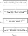
- FIG. 1 illustrates a schematic flowchart of a method of assembling a direct conversion compound semiconductor detector according to an embodiment. The method comprises of steps 20, 21, 22, and 23.
- a direct conversion compound semiconductor sensor (compound semiconductor sensor) is configured over a read out integrated circuit, IC.
- the direct conversion compound semiconductor sensor is made of direct conversion compound semiconductors like Cadmium Telluride (CdTe) or Cadmium Zinc Telluride (CdZnTe) and it comprises a top surface and a bottom surface.
- the direct conversion compound semiconductor sensor is configured to convert high frequency radiation like x-rays incident on its top surface directly into electrical signals transmittable via electrically conductive points, for example, pads on its bottom surface.
- the readout integrated circuit (IC) has two surfaces, a top surface and a bottom surface.
- the readout IC may be hardware logic components such as Field-programmable Gate Arrays (FPGAs), Application-specific Integrated Circuits (ASICs), Application-specific Standard Products (ASSPs), System-on-a-chip systems (SOCs), Complex Programmable Logic Devices (CPLDs), etc.
- FPGAs Field-programmable Gate Arrays
- ASICs Application-specific Integrated Circuits
- ASSPs Application-specific Standard Products
- SOCs System-on-a-chip systems
- CPLDs Complex Programmable Logic Devices
- the top surface of the readout IC has electrical connection points on which solder material may be arranged. Pitch of the solder material so arranged, and the underlying connection points are matched with the pitch of the electrically conductive pads on the bottom surface of the direct conversion compound semiconductor sensor.
- the placement of direct conversion compound semiconductor sensor is done such that the conductive pads on the bottom surface of direct conversion compound semiconductor sensor contact the corresponding solder material on the readout IC.
- the direct conversion compound semiconductor sensor and the readout IC may be bonded by application of physical force. This may not be, however, necessary for some embodiments.
- the physical force applied is high enough to bond the solder material with the conductive pads on the bottom surface of the direct conversion compound semiconductor sensor, at least temporarily.
- the readout IC has circuitry necessary to convert the electrical signals from the direct conversion compound semiconductor sensor into a digital form, adding information including, for example, the location of the signal in a planar co-ordinate system. Further the readout IC has electrical connection points on is bottom surface, through which the digitized signals and information about them may be communicated with further circuitry. These electrical connections may be connected with the circuitry of the readout IC via silicon through vias from the top surface to the bottom surface.
- the solder balls may be configured on the connection points on the bottom of the readout IC, either before step 1 or after step 2
- Step 21 includes illuminating the solder material between the direct conversion compound semiconductor sensor and the readout IC with an Infra-Red (IR) laser for a short duration of time.
- the wavelength of the IR laser is chosen such that the direct conversion compound semiconductor sensor and/or the readout IC is transparent to it.
- the duration for which the IR laser is turned on depends on the melting point of the solder between the direct conversion compound semiconductor sensor and the readout IC.
- the laser illuminates solder material for enough time to heat up and melt the solder material, which after cooling and solidifying forms electrical connections between the connection pads on the bottom surface of the direct conversion compound semiconductor sensor and the connection pads on the top surface of the readout IC.
- the IR laser may be shone on the solder material from the bottom of the readout IC such that the IR passes through the readout IC before illuminating the solder material.
- the IR laser may be shone on the solder material from the top surface of the direct conversion compound semiconductor sensor such that the IR passes through direct conversion compound semiconductor sensor before illuminating the solder material.
- Step 22 includes configuring a substrate material having electrical connection pads corresponding to the solder balls on the bottom surface of the readout IC on the bottom side of the readout IC, matching the pads with the solder balls.
- the substrate may contain circuitry and wiring necessary to connect and transmit the digital signal from the readout IC to processing circuitry, for example for image forming.
- the configuration may further include bonding the substrate with the sensor and readout IC formed in step 21, by means of physical force.
- Step 23 may include illuminating the solder balls between the readout IC and substrate with an IR laser for a duration sufficient to melt the solder material to from electrical connections between connection pads on the bottom surface of the readout IC and the connection pads on the substrate material.
- the IR laser may be configured to illuminate the solder material between the readout IC and the substrate material such that it passes through the substrate material first, for example, the IR laser may be positioned facing the bottom surface of the substrate material.
- the IR laser may be configured to illuminate the solder material between the readout IC and the substrate material such that it passes through the readout IC before reaching the solder material, for example, the IR laser may be positioned facing the top surface of direct conversion compound semiconductor sensor.
- the order of configuring, bonding and illuminating with IR radiation of the direct conversion compound semiconductor sensor and substrate material with the readout IC may be changed along with the direction of illuminating IR radiation.
- the solder material such as the solder alloy may be heated by the IR laser to a pre-set temperature.
- the temperature may be monitored and adjusted by the IR laser fast by fast feedback loop.
- FIG. 2 illustrates components of an individual direct conversion compound semiconductor sensor detector 100 according to an embodiment.
- the individual direct conversion compound semiconductor sensor comprises a direct conversion compound semiconductor sensor 101, a readout IC 105 and a substrate material 111.
- the direct conversion compound semiconductor sensor 101 comprises electrical contact points, for example, in the form of conductive pads (not shown in FIG. 2 ) on its bottom surface to transmit electrical signals produced due to incident high frequency radiation.
- the readout IC 105 comprises two surfaces, the top surface is configured to interface with the bottom surface of the direct conversion compound semiconductor sensor 101 and the bottom surface of the read out IC 105 is configured to interface with the substrate material 111.
- the read out IC 105 comprises solder material 103 configured on its top surface, for example in the form of fine pitch solder spheres.
- solder material 103 are positioned on top of electrical connection points of the readout IC 105 which are configured to receive electrical signals from the direct conversion compound semiconductor sensor 101.
- the readout IC 105 comprises circuitry configured to convert the electrical signals from direct conversion compound semiconductor sensor 101 to a digitized form, which may contain additional information, for example, location of the signal in an X-Y coordinate plane.
- the bottom surface of the readout IC 105 comprises electrical connection points configured to transmit the digitized signal for further processing to the substrate layer 111.
- the bottom surface of readout IC 105 may comprise a redistribution layer, wherein the electrical connection points are connected to the circuitry in readout layer by through silicon vias and conductive metal layers.
- solder material comprising a ball grid array 107 may be configured on the electrical connection points on the bottom of the readout IC 105.
- the substrate material 111 electrical connection points on its surface corresponding to electrical connection points on the bottom surface of readout IC 105. These connection points may comprise electrical pads 109, connected to wiring and circuitry which forwards the digitized signals received from the readout IC 105 for further processing.
- solder material of ball grid array 107 may be configured on the substrate material 111 on corresponding electrical connection points 109 instead of the bottom side of the readout IC 105.
- solder material 103, 107 on the top and bottom surface of readout IC 105, or on top surface of substrate material 109 may be configured using solder jetting.
- solder jetting there may be approximately 121 pieces of solder bumps on the readout IC 105 facing the sensor 101.
- FIG. 3 illustrates a schematic representation of a step of configuring a direct conversion compound semiconductor sensor 101 over a readout IC 105 and reflowing the solder to make electrical connections between the two, according to an embodiment.
- the direct conversion compound semiconductor sensor 101 comprises electrical connection sites, for example in the form of electrical pads, on its bottom surface, configured to transmit electrical signals produced by the high frequency incident and detected by it.
- the read out IC 105 is configured to receive these signals via electrical connection points on its top surface, digitize them and then forward the via electrical connection points on its bottom surface.
- Solder material 103 may be configured on the top surface of the readout IC 105, corresponding to the electrical connection points on the readout IC 105 and connectable to the electrical connection points on the bottom surface of direct conversion compound semiconductor sensor 101.
- Solder material 107 may also be configured on the bottom surface of the readout IC 105 corresponding to the electrical connection points on the bottom surface of the readout IC 105.
- the direct conversion compound semiconductor sensor 101 is positioned on top of the readout IC 105 such that the electrical connection points and the solder material 103 matches.
- the sensor may be bonded using a physical force applied on the direct conversion compound semiconductor sensor 101 and the readout IC 105 against each other.
- the force to be applied may be chosen considering the physical properties of the direct conversion compound semiconductor sensor 101 and the readout IC 105 such that it does not induce stress or cause damage in the direct conversion compound semiconductor sensor 101 and readout IC 105.
- the force to be applied may also be chosen such that a temporary physical adhesion between the solder material 103 and the direct conversion compound semiconductor sensor 101.
- An IR laser 113 with a frequency such that the direct conversion compound semiconductor sensor 101 and/or readout IC 105 is substantially transparent to it is then configured to illuminate the solder material 103.
- the illumination with the IR laser radiation 113 is timed so that it is long enough to melt and reflow the solder material 103, but short enough to not cause thermal damage to the direct conversion compound semiconductor sensor 101 and the readout IC 105.
- the reflow of the solder material 103 forms electrical connections between the electrical connection points on the bottom surface of the direct conversion compound semiconductor sensor 101 and the electrical connection points on the top surface of the readout IC 105.
- the IR radiation 113 may be incident on the direct conversion compound semiconductor sensor 101 and may travel through the direct conversion compound semiconductor sensor 101 to illuminate the solder material 103.
- an IR laser (not shown in FIG. 3 ) may be configured perpendicular to and facing the direct conversion compound semiconductor sensor 101.
- the IR radiation 113 may be incident on the readout IC 105 and may travel through the readout IC 105 to illuminate the solder material 103.
- an IR laser (not shown in FIG. 3 ) may be configured perpendicular to and facing the readout IC 105.
- the solder material 103 or 107 may be configured on the readout IC 105 by using a jetting process, wherein a solder jetting apparatus places individual solder bumps, dots, strip lines or balls on the corresponding electrical connection points as by dispensing solder or solder paste in discrete flows.
- the jetting apparatus may use an IR laser to reflow the solder.
- FIG. 4 illustrates a schematic representation of configuring an assembly 100 comprising a direct conversion compound semiconductor sensor 101 and a readout IC 105, assembled according to embodiments of FIG. 3 , on a substrate material 111 according to an embodiment.
- the substrate material 111 has electrical connection sites which are configured to take the output of readout IC 105 and forward it for, for example, further processing.
- the assembly 102 comprising the direct conversion compound semiconductor sensor 101 and the readout IC 105 assembled in embodiments of FIG. 3 may be placed over the substrate material 111, such that the balls, strip lines or lumps of solder material 107, which are configured on the bottom surface of readout IC 105, are positioned over the corresponding electrical connection points on the substrate material 111.
- the assembly 102 and substrate material 111 may be bonded for example by using a suitable physical force to secure the assembly 102 and the substrate material.
- IR laser radiation from an IR laser then illuminates the solder material 111 to reflow it to form electrical connections between the electrical connection points on the bottom surface of readout IC 105 and the electrical connection points on the top surface of the substrate material 111.
- solder material 107 may be configured on substrate material 111 instead of readout IC 105.
- substrate material 111 may be substantially transparent to IR laser radiation 113, and the IR laser may illuminate solder material 113 after passing through the substrate material 111.
- the IR laser radiation 113 may pass through the direct conversion compound semiconductor sensor 101 and readout IC 105 before illuminating the solder material 111.
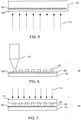
- FIG.s 5, 6 and 7 illustrate steps of assembly of a direct conversion compound semiconductor detector 100 according to another embodiment.
- the direct conversion compound semiconductor detector 100 comprises a direct conversion compound semiconductor sensor 101, configured over a readout IC 105 which is configured over a substrate material 111.
- a direct conversion compound semiconductor sensor 101 is configured over the top surface of a readout IC 105.
- the direct conversion compound semiconductor sensor 101 has electrical connection points on its bottom side to transmit electrical signals corresponding to high frequency incident on and detected by it.
- the readout IC 105 comprises electrical connection points on its top surface configured to receive the electrical signals from the direct conversion compound semiconductor sensor 101, circuitry to digitize the received electrical signals and electrical connection sites on its bottom surface to transmit the digitized signals.
- solder material 103 for example as lumps, spheres, strip lines or balls, may be configured over the electrical connection points, for example by jetting.
- IR radiation 113 from an IR laser illuminates the solder material 103 to reflow it so that electrical connection between electrical connection points on bottom surface of direct conversion compound semiconductor sensor 101 and top surface of readout IC 105 are formed.
- the frequency of IR laser is chosen such that readout IC 105 is substantially transparent to it.
- the duration of illumination by IR radiation 113 is chosen such that solder material 103 is reflowed, but the direct conversion compound semiconductor sensor 101 and the read out IC 105 is not thermally damaged.
- the assembly assembled in embodiments of FIG. 5 may be flipped such that the bottom surface of the readout IC 115 is on top.
- a jetting apparatus 115 then deposits solder material 103, for example solder paste or molten solder, on the electrical connection points on the bottom surface of the readout IC 105.
- a substrate material 111 comprising electrical connection points on its top surface to receive digitized signals from the readout IC is configured on top of the assembly 102 assembled in embodiments of FIG. 5 and 6 such that the electrical connection points match the corresponding balls, strip lines, or lumps or spheres of solder material 107 on the readout IC.
- IR radiation 113 from an IR laser then illuminates the solder material 107 to reflow it and form electrical connections between the electrical connection points on top surface of the substrate material 111 and the electrical connection points on bottom surface of the readout IC 105.
- FIG. 8 illustrates a cross-sectional view of a portion of a complete individual direct conversion compound semiconductor sensor detector 100 as assembled in embodiments of FIG. 1 to FIG. 8 .
- the individual direct conversion compound semiconductor sensor detector 100 comprises a direct conversion compound semiconductor sensor 101, a readout IC 105, a substrate material 111 , solder material 103, 107 and silicon through vias 117, conducing metal layer 121 for distribution and conductive pads 119 over electrical connection points of the direct conversion compound semiconductor sensor 101, readout IC 105 and substrate material 111.
- the direct conversion compound semiconductor sensor 101 is configured over the readout IC 105 and the readout IC 105 is configured over substrate material 111.
- the electrical connection points on the bottom surface of direct conversion compound semiconductor sensor 101, top and bottom surface of readout IC 105 and the top surface substrate layer 111 comprise conductive pads 119.
- the corresponding conductive pads between the bottom surface of direct conversion compound semiconductor sensor 101 and top surface of readout IC 105 are connected to each other via fine pitch solder reflowed by the IR radiation 113.
- the readout IC 105 comprises circuitry to digitize electrical signals received from the direct conversion compound semiconductor sensor 101.
- the circuitry is connected to the bottom surface of readout IC 105 by silicon through vias 117.
- connection pads 119 on bottom of the readout IC 105 are electrically connected to corresponding conductive pads on the top surface of substrate material by solder material 107.
- the solder material 107 may be in the form of a ball grid array.
- the solder material 103 and 107 may have a melting point higher than 150 degree Celsius. This may include solder materials standard lead free solder or eutectic SnPb solders.
- multiple direct conversion compound semiconductor sensor detectors 100 may be arranged in a grid to form a detector array.
- An imaging apparatus may comprise such a detector array, a high frequency radiation source, for example an x-ray source and image processing means for example an image processor.
- An image processor may comprise a standard computer running specialized image processing software or application specific hardware or a mix of the two. Such an imaging apparatus may be used, for example for obtaining x-ray images of live biological tissue or non-biological items like luggage.
- the methods and functionalities described herein may be performed by software in machine readable form on a tangible storage medium e.g. in the form of a computer program comprising computer program code means adapted to perform all the functions and the steps of any of the methods described herein when the program is run on a computer configured to control the necessary manufacturing equipment, for example robotic arms, and where the computer program may be embodied on a computer readable medium.
- tangible storage media include computer storage devices comprising computer-readable media such as disks, thumb drives, memory etc.
- the software can be suitable for execution on a parallel processor or a serial processor such that the method steps may be carried out in any suitable order, or simultaneously.
- a remote computer may store, parts or all of, an example of the process described as software.
- a local or terminal computer may access the remote computer and download a part or all of the software to run the program.
- the local computer may download pieces of the software as needed, or execute some software instructions at the local terminal and some at the remote computer (or computer network).
- the functionally described herein can be performed, at least in part, by one or more hardware logic components.
- FPGAs Field-programmable Gate Arrays
- ASICs Application-specific Integrated Circuits
- ASSPs Application-specific Standard Products
- SOCs System-on-a-chip systems
- CPLDs Complex Programmable Logic Devices
- a method comprises: configuring a direct conversion compound semiconductor sensor over a first surface of a readout integrated circuit, IC, comprising two surfaces, each surface comprising solder material on the surface; illuminating the solder material with an infra-red laser such that the solder material on the readout IC melts and forms solder joints between the readout IC and the direct conversion compound semiconductor sensor; configuring a substrate over a second surface of the readout IC comprising solder material; and illuminating the solder material of the second surface with the infra-red laser such that the solder material on the readout IC melts and electrically connects the readout IC with the substrate.
- the direct conversion compound semiconductor sensor is configured over the first surface of the readout IC and radiation of the infra-red laser passes through the direct conversion compound semiconductor sensor before reaching the solder material on the first surface of the readout IC.
- the substrate is configured over the second surface of the readout IC, and the radiation of the infra-red laser passes through the substrate before reaching the solder material on the second surface of the readout IC.
- the direct conversion compound semiconductor sensor is configured over the first surface of the readout IC and radiation of the infra-red laser passes through the readout IC before reaching the solder material on the first surface of the readout IC.
- the substrate is configured over the second surface of the readout IC, and the radiation of the infra-red laser passes through the substrate before reaching the solder material on the second surface of the readout IC.
- a wavelength of the infra-red laser is chosen such that the direct conversion compound semiconductor sensor is substantially transparent to the infra-red laser.
- the solder material is configured on the two surfaces of the readout IC by jetting.
- the direct conversion compound semiconductor sensor is configured over the first surface of the readout IC by bonding, wherein the bonding comprises placing the direct conversion compound semiconductor sensor over the readout IC so that electrical contact points configured on the bottom surface of the direct conversion compound semiconductor sensor match with the solder material of the readout IC and applying a physical force on the direct conversion compound semiconductor sensor.
- the physical force applied on the direct conversion compound semiconductor sensor is within the range 0 to 100 Newton substantially perpendicular to the surfaces of readout IC.
- the direct conversion compound semiconductor sensor comprises Cadmium Telluride or Cadmium Zinc Telluride.
- the solder alloy has a melting point higher than 150 degree Celsius.
- a computer program comprises a program code configured to perform a method according to the above, when the computer program is executed on a computer controlling hardware required to perform the method.
- a high frequency radiation detector comprises: a direct conversion compound semiconductor sensor; a readout integrated circuit, IC, comprising a first surface and a second surface, the first surface having solder alloy configured on it and the second surface comprise solder alloy; and a substrate having a grid array, assembled by: configuring the direct conversion compound semiconductor sensor over the first surface of the readout IC; illuminating the solder alloy of the first surface with an infra-red laser such that the solder alloy configured on the readout IC melt and form solder joints between readout IC and the direct conversion compound semiconductor sensor; configuring the substrate over the second surface of the readout IC; and illuminating the solder alloy of the second surface with the infra-red laser such that the solder alloy configured on the readout IC melt and electrically connect the readout IC with the substrate.
- the direct conversion compound semiconductor sensor is configured over the first surface of the readout IC and radiation of the infra-red laser passes through the direct conversion compound semiconductor sensor before reaching the solder alloy on the first surface of the readout IC.
- the direct conversion compound semiconductor sensor is configured over the first surface of the readout IC and radiation of the infra-red laser passes through the readout IC before reaching the solder bumps on the first surface of the readout IC.
- an imaging apparatus comprises a radiation source, a detector array and an image processor, wherein the detector array comprises detectors, according to the above, arranged in a grid.
Landscapes
- Engineering & Computer Science (AREA)
- Physics & Mathematics (AREA)
- Optics & Photonics (AREA)
- Mechanical Engineering (AREA)
- Solid State Image Pick-Up Elements (AREA)
- Electric Connection Of Electric Components To Printed Circuits (AREA)
- Wire Bonding (AREA)
- Manufacturing & Machinery (AREA)
- Measurement Of Radiation (AREA)
Priority Applications (5)
| Application Number | Priority Date | Filing Date | Title |
|---|---|---|---|
| EP17153476.1A EP3355342A1 (de) | 2017-01-27 | 2017-01-27 | Laserunterstützte lötverbindung eines direktumwandlungsverbindungshalbleiterdetektors |
| US16/478,676 US11069649B2 (en) | 2017-01-27 | 2018-01-25 | Laser assisted solder bonding of direct conversion compound semiconductor detector |
| PCT/EP2018/051765 WO2018138174A1 (en) | 2017-01-27 | 2018-01-25 | Laser assisted solder bonding of direct conversion compound semiconductor detector |
| JP2019539828A JP2020508560A (ja) | 2017-01-27 | 2018-01-25 | 直接変換型化合物半導体検出器のレーザアシストはんだ接合 |
| CN201880008432.3A CN110226221A (zh) | 2017-01-27 | 2018-01-25 | 直接转换化合物半导体探测器的激光辅助焊料接合 |
Applications Claiming Priority (1)
| Application Number | Priority Date | Filing Date | Title |
|---|---|---|---|
| EP17153476.1A EP3355342A1 (de) | 2017-01-27 | 2017-01-27 | Laserunterstützte lötverbindung eines direktumwandlungsverbindungshalbleiterdetektors |
Publications (1)
| Publication Number | Publication Date |
|---|---|
| EP3355342A1 true EP3355342A1 (de) | 2018-08-01 |
Family
ID=57963010
Family Applications (1)
| Application Number | Title | Priority Date | Filing Date |
|---|---|---|---|
| EP17153476.1A Withdrawn EP3355342A1 (de) | 2017-01-27 | 2017-01-27 | Laserunterstützte lötverbindung eines direktumwandlungsverbindungshalbleiterdetektors |
Country Status (5)
| Country | Link |
|---|---|
| US (1) | US11069649B2 (de) |
| EP (1) | EP3355342A1 (de) |
| JP (1) | JP2020508560A (de) |
| CN (1) | CN110226221A (de) |
| WO (1) | WO2018138174A1 (de) |
Families Citing this family (2)
| Publication number | Priority date | Publication date | Assignee | Title |
|---|---|---|---|---|
| KR102528016B1 (ko) * | 2018-10-05 | 2023-05-02 | 삼성전자주식회사 | 솔더 부재 실장 방법 및 시스템 |
| US12557646B2 (en) * | 2022-08-31 | 2026-02-17 | Taiwan Semiconductor Manufacturing Company, Ltd. | Multi-die package and methods of formation |
Citations (6)
| Publication number | Priority date | Publication date | Assignee | Title |
|---|---|---|---|---|
| DE4446289A1 (de) * | 1994-12-23 | 1996-06-27 | Finn David | Verfahren und Vorrichtung zur Mikroverbindung von Kontaktelementen |
| US20070037318A1 (en) * | 2005-08-11 | 2007-02-15 | Samsung Techwin Co., Ltd. | Method and apparatus for flip-chip bonding |
| JP2007214271A (ja) * | 2006-02-08 | 2007-08-23 | Zycube:Kk | 基板の接合方法および半導体装置 |
| DE102008050838A1 (de) * | 2008-10-08 | 2009-10-15 | Siemens Aktiengesellschaft | Elektrische Baugruppe, Röntgenmesssystem, Computertomograph sowie Verfahren zur Fertigung einer elektrischen Baugruppe |
| US20120133001A1 (en) * | 2010-11-30 | 2012-05-31 | General Electric Company | Tileable sensor array |
| US20160015339A1 (en) * | 2014-07-15 | 2016-01-21 | Siemens Aktiengesellschaft | Imaging device for electromagnetic radiation |
Family Cites Families (4)
| Publication number | Priority date | Publication date | Assignee | Title |
|---|---|---|---|---|
| JP2001332574A (ja) * | 2000-05-23 | 2001-11-30 | Mitsubishi Electric Corp | バンプ形成装置およびバンプ形成方法 |
| JP2003255051A (ja) * | 2002-02-28 | 2003-09-10 | Shimadzu Corp | 2次元アレイ型放射線検出器 |
| US20120193545A1 (en) * | 2011-01-31 | 2012-08-02 | General Electric Company | Detector systems with anode incidence face and methods of fabricating the same |
| US9916989B2 (en) * | 2016-04-15 | 2018-03-13 | Amkor Technology, Inc. | System and method for laser assisted bonding of semiconductor die |
-
2017
- 2017-01-27 EP EP17153476.1A patent/EP3355342A1/de not_active Withdrawn
-
2018
- 2018-01-25 US US16/478,676 patent/US11069649B2/en not_active Expired - Fee Related
- 2018-01-25 JP JP2019539828A patent/JP2020508560A/ja active Pending
- 2018-01-25 WO PCT/EP2018/051765 patent/WO2018138174A1/en not_active Ceased
- 2018-01-25 CN CN201880008432.3A patent/CN110226221A/zh active Pending
Patent Citations (6)
| Publication number | Priority date | Publication date | Assignee | Title |
|---|---|---|---|---|
| DE4446289A1 (de) * | 1994-12-23 | 1996-06-27 | Finn David | Verfahren und Vorrichtung zur Mikroverbindung von Kontaktelementen |
| US20070037318A1 (en) * | 2005-08-11 | 2007-02-15 | Samsung Techwin Co., Ltd. | Method and apparatus for flip-chip bonding |
| JP2007214271A (ja) * | 2006-02-08 | 2007-08-23 | Zycube:Kk | 基板の接合方法および半導体装置 |
| DE102008050838A1 (de) * | 2008-10-08 | 2009-10-15 | Siemens Aktiengesellschaft | Elektrische Baugruppe, Röntgenmesssystem, Computertomograph sowie Verfahren zur Fertigung einer elektrischen Baugruppe |
| US20120133001A1 (en) * | 2010-11-30 | 2012-05-31 | General Electric Company | Tileable sensor array |
| US20160015339A1 (en) * | 2014-07-15 | 2016-01-21 | Siemens Aktiengesellschaft | Imaging device for electromagnetic radiation |
Non-Patent Citations (1)
| Title |
|---|
| ZEQUN MEI ET AL: "LOW-TEMPERATURE SOLDERS", HEWLETT-PACKARD JOURNAL, HEWLETT-PACKARD CO. PALO ALTO, US, vol. 47, no. 4, 1 August 1996 (1996-08-01), pages 91 - 98, XP000621968 * |
Also Published As
| Publication number | Publication date |
|---|---|
| WO2018138174A1 (en) | 2018-08-02 |
| US20190378815A1 (en) | 2019-12-12 |
| US11069649B2 (en) | 2021-07-20 |
| CN110226221A (zh) | 2019-09-10 |
| JP2020508560A (ja) | 2020-03-19 |
Similar Documents
| Publication | Publication Date | Title |
|---|---|---|
| US7531809B2 (en) | Gamma ray detector modules | |
| Chen et al. | Electromigration and thermomigration in Pb-free flip-chip solder joints | |
| CN105534540B (zh) | 用于制造检测器模块的传感器板的方法 | |
| US8975583B2 (en) | 3D stacked uncooled IR sensor device and method | |
| US10371578B2 (en) | Thermal management of thermal sensor in a mobile device | |
| US11069649B2 (en) | Laser assisted solder bonding of direct conversion compound semiconductor detector | |
| Jang et al. | Development and optimization of the laser-assisted bonding process for a flip chip package | |
| Marchal et al. | EXCALIBUR: a small-pixel photon counting area detector for coherent X-ray diffraction-Front-end design, fabrication and characterisation | |
| JP5350604B2 (ja) | 半導体装置及びその製造方法 | |
| Stoyanov et al. | Modeling Insights into the assembly challenges of focal plane arrays | |
| CN109478556B (zh) | 检测器模块、检测器、成像设备和制造检测器模块的方法 | |
| US6822315B2 (en) | Apparatus and method for scribing semiconductor wafers using vision recognition | |
| Kim et al. | Development of extremely thin profile flip chip CSP using laser assisted bonding technology | |
| Lewis et al. | New design yields robust large-area framing camera | |
| US6597444B1 (en) | Determination of flux coverage | |
| US20210366743A1 (en) | Semiconductor packaging apparatus and method of manufacturing semiconductor device using the same | |
| Mottet | Flip-Chip Assembly for Focal Plane Array | |
| TW202349696A (zh) | 影像感測器封裝 | |
| Howell et al. | Area array solder interconnection technology for the three-dimensional silicon cube | |
| TWI880183B (zh) | 一種熱膨脹測量系統 | |
| Wood | Heterogenous Integration at Sandia? s MESA Facility. | |
| Lecarpentier et al. | Die to Die and Die To Wafer Bonding Solution for High Density, Fine Pitch Micro-Bumped Die | |
| Sathe et al. | A study of the thermal characteristics of a conductive adhesive chip attach process | |
| Kwiatkowski et al. | 3-D electronics interconnect for high-performance imaging detectors | |
| CZ310034B6 (cs) | Způsob výroby elektricky vodivých spojů s 3D uspořádáním mezi komponentami detektoru ionizujícího záření a detektor s elektricky vodivými spoji vyrobenými tímto způsobem |
Legal Events
| Date | Code | Title | Description |
|---|---|---|---|
| PUAI | Public reference made under article 153(3) epc to a published international application that has entered the european phase |
Free format text: ORIGINAL CODE: 0009012 |
|
| STAA | Information on the status of an ep patent application or granted ep patent |
Free format text: STATUS: THE APPLICATION HAS BEEN PUBLISHED |
|
| AK | Designated contracting states |
Kind code of ref document: A1 Designated state(s): AL AT BE BG CH CY CZ DE DK EE ES FI FR GB GR HR HU IE IS IT LI LT LU LV MC MK MT NL NO PL PT RO RS SE SI SK SM TR |
|
| AX | Request for extension of the european patent |
Extension state: BA ME |
|
| STAA | Information on the status of an ep patent application or granted ep patent |
Free format text: STATUS: REQUEST FOR EXAMINATION WAS MADE |
|
| 17P | Request for examination filed |
Effective date: 20181212 |
|
| RBV | Designated contracting states (corrected) |
Designated state(s): AL AT BE BG CH CY CZ DE DK EE ES FI FR GB GR HR HU IE IS IT LI LT LU LV MC MK MT NL NO PL PT RO RS SE SI SK SM TR |
|
| STAA | Information on the status of an ep patent application or granted ep patent |
Free format text: STATUS: EXAMINATION IS IN PROGRESS |
|
| 17Q | First examination report despatched |
Effective date: 20201014 |
|
| STAA | Information on the status of an ep patent application or granted ep patent |
Free format text: STATUS: THE APPLICATION IS DEEMED TO BE WITHDRAWN |
|
| 18D | Application deemed to be withdrawn |
Effective date: 20240312 |