EP3355480A1 - Dispositif de communication, procédé de traitement de communication, appareil de traitement de communication et système de communication - Google Patents
Dispositif de communication, procédé de traitement de communication, appareil de traitement de communication et système de communication Download PDFInfo
- Publication number
- EP3355480A1 EP3355480A1 EP15910095.7A EP15910095A EP3355480A1 EP 3355480 A1 EP3355480 A1 EP 3355480A1 EP 15910095 A EP15910095 A EP 15910095A EP 3355480 A1 EP3355480 A1 EP 3355480A1
- Authority
- EP
- European Patent Office
- Prior art keywords
- main control
- control board
- integrated main
- sfu
- mcu
- Prior art date
- Legal status (The legal status is an assumption and is not a legal conclusion. Google has not performed a legal analysis and makes no representation as to the accuracy of the status listed.)
- Granted
Links
Images



Classifications
-
- H—ELECTRICITY
- H04—ELECTRIC COMMUNICATION TECHNIQUE
- H04L—TRANSMISSION OF DIGITAL INFORMATION, e.g. TELEGRAPHIC COMMUNICATION
- H04L41/00—Arrangements for maintenance, administration or management of data switching networks, e.g. of packet switching networks
- H04L41/06—Management of faults, events, alarms or notifications
- H04L41/0695—Management of faults, events, alarms or notifications the faulty arrangement being the maintenance, administration or management system
-
- G—PHYSICS
- G06—COMPUTING OR CALCULATING; COUNTING
- G06F—ELECTRIC DIGITAL DATA PROCESSING
- G06F11/00—Error detection; Error correction; Monitoring
- G06F11/07—Responding to the occurrence of a fault, e.g. fault tolerance
- G06F11/0703—Error or fault processing not based on redundancy, i.e. by taking additional measures to deal with the error or fault not making use of redundancy in operation, in hardware, or in data representation
- G06F11/0751—Error or fault detection not based on redundancy
-
- G—PHYSICS
- G06—COMPUTING OR CALCULATING; COUNTING
- G06F—ELECTRIC DIGITAL DATA PROCESSING
- G06F11/00—Error detection; Error correction; Monitoring
- G06F11/07—Responding to the occurrence of a fault, e.g. fault tolerance
- G06F11/16—Error detection or correction of the data by redundancy in hardware
- G06F11/20—Error detection or correction of the data by redundancy in hardware using active fault-masking, e.g. by switching out faulty elements or by switching in spare elements
- G06F11/2002—Error detection or correction of the data by redundancy in hardware using active fault-masking, e.g. by switching out faulty elements or by switching in spare elements where interconnections or communication control functionality are redundant
- G06F11/2005—Error detection or correction of the data by redundancy in hardware using active fault-masking, e.g. by switching out faulty elements or by switching in spare elements where interconnections or communication control functionality are redundant using redundant communication controllers
-
- G—PHYSICS
- G06—COMPUTING OR CALCULATING; COUNTING
- G06F—ELECTRIC DIGITAL DATA PROCESSING
- G06F11/00—Error detection; Error correction; Monitoring
- G06F11/07—Responding to the occurrence of a fault, e.g. fault tolerance
- G06F11/16—Error detection or correction of the data by redundancy in hardware
- G06F11/20—Error detection or correction of the data by redundancy in hardware using active fault-masking, e.g. by switching out faulty elements or by switching in spare elements
- G06F11/202—Error detection or correction of the data by redundancy in hardware using active fault-masking, e.g. by switching out faulty elements or by switching in spare elements where processing functionality is redundant
- G06F11/2023—Failover techniques
- G06F11/2028—Failover techniques eliminating a faulty processor or activating a spare
-
- G—PHYSICS
- G06—COMPUTING OR CALCULATING; COUNTING
- G06F—ELECTRIC DIGITAL DATA PROCESSING
- G06F11/00—Error detection; Error correction; Monitoring
- G06F11/07—Responding to the occurrence of a fault, e.g. fault tolerance
- G06F11/16—Error detection or correction of the data by redundancy in hardware
- G06F11/20—Error detection or correction of the data by redundancy in hardware using active fault-masking, e.g. by switching out faulty elements or by switching in spare elements
- G06F11/202—Error detection or correction of the data by redundancy in hardware using active fault-masking, e.g. by switching out faulty elements or by switching in spare elements where processing functionality is redundant
- G06F11/2023—Failover techniques
- G06F11/2033—Failover techniques switching over of hardware resources
-
- G—PHYSICS
- G06—COMPUTING OR CALCULATING; COUNTING
- G06F—ELECTRIC DIGITAL DATA PROCESSING
- G06F11/00—Error detection; Error correction; Monitoring
- G06F11/07—Responding to the occurrence of a fault, e.g. fault tolerance
- G06F11/16—Error detection or correction of the data by redundancy in hardware
- G06F11/20—Error detection or correction of the data by redundancy in hardware using active fault-masking, e.g. by switching out faulty elements or by switching in spare elements
- G06F11/2097—Error detection or correction of the data by redundancy in hardware using active fault-masking, e.g. by switching out faulty elements or by switching in spare elements maintaining the standby controller/processing unit updated
-
- H—ELECTRICITY
- H04—ELECTRIC COMMUNICATION TECHNIQUE
- H04B—TRANSMISSION
- H04B1/00—Details of transmission systems, not covered by a single one of groups H04B3/00 - H04B13/00; Details of transmission systems not characterised by the medium used for transmission
- H04B1/74—Details of transmission systems, not covered by a single one of groups H04B3/00 - H04B13/00; Details of transmission systems not characterised by the medium used for transmission for increasing reliability, e.g. using redundant or spare channels or apparatus
-
- H—ELECTRICITY
- H04—ELECTRIC COMMUNICATION TECHNIQUE
- H04L—TRANSMISSION OF DIGITAL INFORMATION, e.g. TELEGRAPHIC COMMUNICATION
- H04L41/00—Arrangements for maintenance, administration or management of data switching networks, e.g. of packet switching networks
- H04L41/06—Management of faults, events, alarms or notifications
- H04L41/0654—Management of faults, events, alarms or notifications using network fault recovery
- H04L41/0659—Management of faults, events, alarms or notifications using network fault recovery by isolating or reconfiguring faulty entities
- H04L41/0661—Management of faults, events, alarms or notifications using network fault recovery by isolating or reconfiguring faulty entities by reconfiguring faulty entities
Definitions
- the present invention relates to the field of communications technologies, and in particular, to a communications device, a communication processing method, a communication processing apparatus, and a communications system.
- a management and control processing unit (Maintain and control Process Unit, MCU), a fabric unit (Fabric Unit, FU), and an uplink service forwarding unit (Service forwarding Unit, SFU) are integrated on a physical main control board of a rack communications device.
- the MCU has management and control functions, and may control the FU and the SFU. Therefore, in-service software upgrade (In-Service Software Upgrade, ISSU) usually needs to be performed on the MCU. An MCU fault or reset occurs sometimes. In an ISSU process, when the MCU encounters a fault or is reset, a service packet loss usually occurs if a service volume is relatively large. Consequently, normal operation of a communication service is affected.
- ISSU Intelligent Software Upgrade
- Embodiments of the present invention provide a communications device, a communication processing method, a communication processing apparatus, and a communications system, to alleviate a service packet loss when an MCU encounters a fault or is reset in an ISSU process.
- a communications device includes at least two integrated main control boards.
- An MCU and a hardware forwarding unit are integrated on each of the integrated main control boards, and the hardware forwarding unit includes an FU and an SFU.
- a control signal exchange path is provided between the MCU on each integrated main control board and a hardware forwarding unit on another integrated main control board in the at least two integrated main control boards.
- an MCU on any one of the at least two integrated main control boards can control an FU and an SFU on the another integrated main control board in the at least two integrated main control boards by using the control signal exchange path.
- an integrated main control board on which an MCU works normally may take over to control an FU and an SFU on the integrated main control board on which the MCU encounters a fault or is reset and ISSU is performed on the MCU, thereby avoiding a problem that an MCU fault or reset and ISSU affect an FU and an SFU, and consequently a forwarding capability is reduced by half and a service packet loss is caused.
- a selector is further provided on the integrated main control board, and the FU and the SFU choose, by using the selector, to be controlled by an MCU by using the control signal exchange path, where the MCU is on another integrated main control board in the at least two integrated main control boards that is different from an integrated main control board on which the FU and the SFU are integrated.
- the selector is provided so that according to an actual application scenario, the FU and the SFU may choose to be controlled by an MCU on the integrated main control board on which the FU and the SFU are integrated, or choose to be controlled by an MCU on another integrated main control board.
- a selector is further provided on the integrated main control board, and an MCU on any one of the at least two integrated main control boards configures a selector on another integrated main control board in the at least two integrated main control boards, to choose to control, by using the control signal exchange path, an FU and an SFU on the another integrated main control board in the at least two integrated main control boards.
- the selector is provided so that the MCU may choose, according to an actual application scenario, to control the FU and SFU on the another integrated main control board. Therefore, the MCU may control only an FU and an SFU on the integrated main control board on which the MCU is integrated, or the MCU may control both an FU and an SFU on the integrated main control board on which the MCU is integrated, and the FU and the SFU on the another integrated main control board.
- the selector is a selector switch.
- the control signal exchange path is a control bus.
- a communication method is provided. The method may be applied to communication between at least two integrated main control boards. A control signal exchange path is provided between the at least two integrated main control boards.
- An MCU on an integrated main control board determines that an FU and an SFU on another integrated main control board different from the integrated main control board need to be controlled. The MCU on the integrated main control board controls the FU and the SFU on the another integrated main control board different from the integrated main control board by using the control signal exchange path.
- the present invention can avoid a problem that an MCU fault or reset and ISSU affect an FU and an SFU, and consequently a forwarding capability is reduced by half and a service packet loss is caused.
- the MCU on the integrated main control board may determine that the FU and the SFU on the another integrated main control board different from the integrated main control board need to be controlled.
- the controlling, by the MCU on the integrated main control board, the FU and the SFU on the another integrated main control board different from the integrated main control board by using the control signal exchange path includes: controlling, by the MCU on the integrated main control board by using the control signal exchange path, the FU and the SFU on the another integrated main control board different from the integrated main control board to clear original hardware configuration data; and sending, by the MCU on the integrated main control board by using the control signal exchange path, pre-stored hardware configuration data to the FU and the SFU on the another integrated main control board different from the integrated main control board.
- the pre-stored hardware configuration data is hardware configuration data of the FU and the SFU on the another integrated main control board different from the integrated main control board.
- the controlling, by the MCU on the integrated main control board, the FU and the SFU on the another integrated main control board different from the integrated main control board by using the control signal exchange path includes: obtaining, by the MCU on the integrated main control board by using the control signal exchange path, original hardware configuration data of the FU and the SFU on the another integrated main control board different from the integrated main control board; and performing, by the MCU on the integrated main control board, consistency verification on pre-stored hardware configuration data and the original hardware configuration data, and updating original hardware configuration data different from the pre-stored hardware configuration data with reference to the pre-stored hardware configuration data.
- the pre-stored hardware configuration data is hardware configuration data of the FU and the SFU on the another integrated main control board different from the integrated main control board.
- the MCU on the integrated main control board pre-stores, in a form of a mirror table, the hardware configuration data of the FU and the SFU on the another integrated main control board different from the integrated main control board.
- the MCU on the integrated main control board configures a selector on the another integrated main control board different from the integrated main control board, to choose to control, by using the control signal exchange path, the FU and the SFU on the another integrated main control board different from the integrated main control board.
- a communication processing apparatus applied to an integrated main control board.
- the communication processing apparatus includes a determining unit and a control unit.
- the determining unit is configured to determine that a fabric unit FU and a service forwarding unit SFU on another integrated main control board different from the integrated main control board need to be controlled.
- the control unit is configured to: when the determining unit determines that the FU and the SFU on the another integrated main control board different from the integrated main control board need to be controlled, control the FU and the SFU on the another integrated main control board different from the integrated main control board by using a control signal exchange path.
- the control signal exchange path is provided between an MCU on the integrated main control board and a hardware forwarding unit on the another integrated main control board different from the integrated main control board, and the hardware forwarding unit includes the FU and the SFU.
- control unit is specifically configured to: if determining that an MCU on the another integrated main control board different from the integrated main control board is in an abnormal working state, and that at least one of the FU or the SFU on the another integrated main control board different from the integrated main control board is in a normal working state, determine that the FU and the SFU on the another integrated main control board different from the integrated main control board need to be controlled.
- control unit is specifically configured to: control, by using the control signal exchange path, the FU and the SFU on the another integrated main control board different from the integrated main control board to clear original hardware configuration data; and send, by using the control signal exchange path, pre-stored hardware configuration data to the FU and the SFU on the another integrated main control board different from the integrated main control board.
- the pre-stored hardware configuration data is hardware configuration data of the FU and the SFU on the another integrated main control board different from the integrated main control board.
- control unit is specifically configured to: obtain, by using the control signal exchange path, original hardware configuration data of the FU and the SFU on the another integrated main control board different from the integrated main control board; and perform consistency verification on pre-stored hardware configuration data and the original hardware configuration data, and update original hardware configuration data different from the pre-stored hardware configuration data with reference to the pre-stored hardware configuration data.
- the pre-stored hardware configuration data is hardware configuration data of the FU and the SFU on the another integrated main control board different from the integrated main control board.
- control unit is further configured to: before controlling the FU and the SFU on the another integrated main control board different from the integrated main control board by using the control signal exchange path, configure a selector on the another integrated main control board different from the integrated main control board, to choose to control, by using the control signal exchange path, the FU and the SFU on the another integrated main control board different from the integrated main control board.
- the communication processing apparatus further includes a storage unit.
- the storage unit is configured to pre-store, in a form of a mirror table, the hardware configuration data of the FU and the SFU on the another integrated main control board different from the integrated main control board.
- a communications system including at least two communications units.
- Each communications unit includes a management and control processing unit MCU and a hardware forwarding unit
- the hardware forwarding unit includes a fabric unit FU and a service forwarding unit SFU.
- a control signal exchange path is provided between the MCU on each communications unit and a hardware forwarding unit on another communications unit in the at least two communications units; and an MCU on any one of the at least two communications units controls an FU and an SFU on the another communications unit in the at least two communications units by using the control signal exchange path.
- a communication processing apparatus includes a processor and a memory.
- the memory stores a computer readable program, and the processor performs the communication processing method according to the second aspect by running the program in the memory.
- a computer storage medium configured to store a computer software instruction used for the foregoing communication processing method, and including a program designed to perform the foregoing communication processing method according to the second aspect.
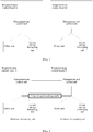
- FIG. 1 an architecture shown in FIG. 1 is usually used for a rack communications system.
- the rack communications system includes two or more integrated main control boards.
- Two integrated main control boards are used as an example in FIG. 1 for description.
- the two integrated main control boards serve as a primary integrated main control board and a secondary integrated main control board. That is, the two integrated main control boards include a primary integrated main control board and a secondary integrated main control board.
- a management and control processing unit (Maintain and control Process Unit, MCU), a fabric unit (Fabric Unit, FU), and an uplink service forwarding unit (Service forwarding Unit, SFU) are integrated on each integrated main control board.
- the MCU on each integrated main control board manages and controls an FU and an SFU on the integrated main control board on which the MCU is located.
- an ISSU process, an MCU fault, or an MCU reset occurs, the entire physical main control board on which the MCU, the FU, and the SFU are integrated needs to be reset. Consequently, the FU and the SFU on a forwarding plane on the physical main control board also stop working.
- a forwarding service can be restored only after the MCU restores and completes related configurations.
- a connected service can be forwarded only by using an FU and an SFU on another integrated main control board. Therefore, a forwarding capability is deteriorated.
- a service packet loss occurs when a service volume is relatively large and exceeds a forwarding capability of the FU and the SFU on the another integrated main control board.
- a control signal exchange path is added between the primary integrated main control board and the secondary integrated main control board.
- the MCU on each integrated main control board may control an FU and an SFU on another integrated main control board by using the control signal exchange path, so as to resolve the problem that an MCU fault or reset and ISSU affect an FU and an SFU, and consequently a forwarding capability is reduced by half and a service packet loss is caused.
- FIG. 2 is a schematic structural diagram of a communications device according to an embodiment of the present invention.
- the communications device includes an integrated main control board A and an integrated main control board B.
- the integrated main control board A and the integrated main control board B may be integrated main control boards that serve as a primary integrated main control board and a secondary integrated main control board.
- An MCU and a hardware forwarding unit are integrated on both the integrated main control board A and the integrated main control board B.
- the hardware forwarding unit includes an FU and an SFU.
- a control signal exchange path is provided between the MCU on either integrated main control board and a hardware forwarding unit on the other integrated main control board.
- the MCU on either integrated main control board can control an FU and an SFU on the other integrated main control board by using the control signal exchange path.
- the communications device may include more than two integrated main control boards. That is, the communications device provided in this embodiment of the present invention includes at least two integrated main control boards.
- An MCU, an FU, and an SFU are integrated on each of the integrated main control boards.
- a control signal exchange path is provided between the MCU on each integrated main control board and a hardware forwarding unit on another integrated main control board in the at least two integrated main control boards.
- An MCU on any one of the at least two integrated main control boards controls an FU and an SFU on the another integrated main control board in the at least two integrated main control boards by using the control signal exchange path.
- control signal exchange path is provided between the integrated main control boards, so that an MCU on any integrated main control board not only can manage an FU and an SFU integrated on the integrated main control board on which the MCU is located, but also can manage an FU and an SFU on another integrated main control board.
- an MCU on another integrated main control board may manage and control an FU and an SFU on the integrated main control board on which the MCU fault or reset or the ISSU process occurs, so as to maintain a normal forwarding capability of the FU and the SFU on the integrated main control board on which the MCU fault or reset or the ISSU process occurs, and avoid a service packet loss caused by an insufficient forwarding capability.
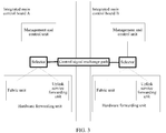
- FIG. 3 is a schematic structural diagram of another rack communications device according to an embodiment of the present invention.
- a selector may further be provided on each integrated main control board, so that by means of the selector, an FU and an SFU on each integrated main control board may choose to be controlled by an MCU on the integrated main control board on which the FU and the SFU are integrated, or choose to be controlled by an MCU on another integrated main control board by using the control signal exchange path. That is, the FU and the SFU on each integrated main control board can be managed and controlled only by the MCU on the integrated main control board on which the FU and the SFU are integrated or by the MCU on the another integrated main control board at a time.
- the MCU on each integrated main control board may control only an FU and an SFU on the integrated main control board on which the MCU is integrated, or may control both an FU and an SFU on the integrated main control board on which the MCU is integrated, and an FU and an SFU on another integrated main control board.
- an FU and an SFU on another integrated main control board may exchange information with an MCU on another integrated main control board by using the control signal exchange path.
- the FU and the SFU on the integrated main control board actively choose, by using the selector, to be controlled by using the control signal exchange path by the MCU on the another integrated main control board different from the integrated main control board on which the FU and the SFU are integrated.
- an MCU on any one of the at least two integrated main control boards may configure a selector on another integrated main control board in the at least two integrated main control boards, to choose to control, by using the control signal exchange path, an FU and an SFU on the another integrated main control board in the at least two integrated main control boards.
- a selector is provided on an integrated main control board, so that an FU and an SFU on the integrated main control board can be managed and controlled only by an MCU on the integrated main control board on which the FU and the SFU are integrated or by an MCU on another integrated main control board at a time. Therefore, when the MCU on the integrated main control board on which the FU and the SFU are integrated is normal, the MCU on the integrated main control board on which the FU and the SFU are integrated can manage and control the FU and the SFU on the current board. When the MCU on the integrated main control board on which the FU and the SFU are integrated is abnormal, the MCU on the another integrated main control board can manage and control the FU and the SFU on the current board.
- a specific integrated main control board whose MCU performs management and control may be negotiated and determined according to a specific service scenario.
- control signal exchange path may be a control bus
- selector may be a selector switch
- the rack communications device includes a primary integrated main control board and a secondary integrated main control board is used for description.
- FIG. 4 is a schematic diagram of a working status when both MCUs on a primary integrated main control board and a secondary integrated main control board are in a normal working state.
- the MCUs on the primary integrated main control board and the secondary integrated main control board each include a management and control subsystem and a forwarding drive subsystem in terms of software implementation.
- the management and control subsystem is mainly configured to perform data synchronization on a control plane between the primary integrated main control board and the secondary integrated main control board.
- the forwarding drive subsystem is mainly configured to perform data synchronization on a forwarding plane between the primary integrated main control board and the secondary integrated main control board.
- the management and control subsystem of the MCU on the primary integrated main control board is responsible for managing and generating resources and entry data on the forwarding plane, and synchronizing the resources and the entry data to the secondary integrated main control board by using an inter-board synchronization path.
- the forwarding drive subsystems of the MCUs on the primary integrated main control board and the secondary integrated main control board separately configure hardware configuration data of hardware forwarding units (FUs and SFUs).
- each of the MCUs on the primary integrated main control board and the secondary integrated main control board not only needs to store hardware configuration data of an FU and an SFU on an integrated main control board on which the MCU is integrated, but also needs to store hardware configuration data of an FU and an SFU on another integrated main control board.
- the hardware configuration data of the FU and the SFU on the another integrated main control board is pre-stored in a form of a mirror table.
- the forwarding drive subsystem of the MCU is further configured to maintain a chip status of a hardware forwarding unit (an FU and an SFU).
- the chip status represents a state machine of the hardware forwarding unit, and includes a real chip state and a virtual chip state.
- the real chip state represents that the current MCU controls the hardware forwarding unit. In this case, the MCU needs to send corresponding hardware configuration data to the hardware forwarding unit, and store the corresponding hardware configuration data in a mirror database for hardware configuration data in a main memory.
- the virtual chip state represents that the current MCU does not control the hardware forwarding unit.
- the MCU does not need to send corresponding hardware configuration data to the hardware forwarding unit, and only needs to store the corresponding hardware configuration data in a mirror database for hardware configuration data in a main memory. Therefore, when each of the MCUs on the primary integrated main control board and the secondary integrated main control board is in a normal working state, a chip status of a hardware forwarding unit on an integrated main control board on which the MCU is integrated is the real chip state, and a chip status of a hardware forwarding unit on another integrated main control board is the virtual chip state.
- a control signal exchange path is provided between the primary integrated main control board and the secondary integrated main control board.
- the control signal exchange path is provided between an MCU on each integrated main control board and a hardware forwarding unit on another integrated main control board different from the integrated main control board.
- the hardware forwarding unit includes the FU and the SFU. Therefore, a communication processing method shown in FIG. 5 may be used in this embodiment of the present invention. As shown in FIG. 5 , the method includes the following steps.
- S101 An MCU on an integrated main control board determines that an FU and an SFU on another integrated main control board different from the integrated main control board need to be controlled.
- a control signal exchange path is provided between a primary integrated main control board and a secondary integrated main control board. Therefore, a hardware-based exchange mechanism for a status signal may be added between the primary integrated main control board and the secondary integrated main control board.
- the status signal is used to represent whether the MCU, the FU, and the SFU are in a normal working state or a fault state.
- An MCU in a normal working state detects status signals of an MCU, an FU, and an SFU integrated on another integrated main control board, and determines, by using the status signals, working statuses of the MCU, the FU, and the SFU integrated on the another integrated main control board. If detecting that the MCU on the another integrated main control board is in a fault state, and that at least one of the FU or the SFU is in a normal working state, the MCU in the normal working state determines that the FU and the SFU that are integrated on the another integrated main control board need to be controlled.
- the MCU on the integrated main control board controls the FU and the SFU on the another integrated main control board different from the integrated main control board by using a control signal exchange path.
- the MCU on the integrated main control board may choose, by using a selector, whether to control the FU and the SFU on the another integrated main control board.
- the selector may be set to choose to connect to the control signal exchange path, and to control the FU and the SFU that are integrated on the another integrated main control board by using the control signal exchange path.
- the MCU in the normal working state configures the selector, chooses, by using the selector, to connect to the control signal exchange path, and controls, by using the control signal exchange path, the FU and the SFU that are integrated on the another integrated main control board and that are in the normal working state to clear original hardware configuration data.
- the MCU in the normal working state sends, by using the control signal exchange path, pre-stored hardware configuration data of the fabric and the SFU on the another integrated main control board to the FU and the SFU that are integrated on the another integrated main control board.
- the MCU in the normal working state configures the selector, and chooses, by using the selector, to connect to the control signal exchange path.
- the MCU in the normal working state obtains, by using the control signal exchange path, original hardware configuration data of the FU and the SFU that are integrated on the another integrated main control board and that are in the normal working state, performs consistency verification on the pre-stored hardware configuration data of the fabric and the SFU on the another integrated main control board and the original hardware configuration data, and updates original hardware configuration data different from the pre-stored hardware configuration data with reference to the pre-stored hardware configuration data.
- FIG. 6 is a schematic diagram of a working status when the MCU on the secondary integrated main control board is abnormal. As shown in FIG.
- a forwarding drive subsystem of the MCU on the primary integrated main control board sends, to a corresponding hardware forwarding unit, mirror data that is of a hardware forwarding unit on the another integrated main control board and that is pre-stored in a hardware mirror database for hardware configuration data, and switches a chip status of the hardware forwarding unit on the another integrated main control board to a real chip state.
- the MCU on the secondary integrated main control board may control the FU and the SFU on the secondary integrated main control board again.
- data synchronization on the control plane and data synchronization on the forwarding plane need to be completed between the primary integrated main control board and the secondary integrated main control board need to be completed.
- FIG. 7 is a schematic diagram of a working status in a process of performing data synchronization between the primary integrated main control board and the secondary integrated main control board.
- FIG. 6 and FIG. 7 an example in which the MCU on the secondary integrated main control board encounters a fault is used for description.
- a switch between the primary integrated main control board and the secondary integrated main control board may be first performed, and after the switch between the primary integrated main control board and the secondary integrated main control board is performed, processing may be then performed according to the processing manner in the foregoing embodiment. Details are not described herein again.
- an embodiment of the present invention further provides a communication processing apparatus 100.
- the communication processing apparatus 100 is applied to an integrated main control board.
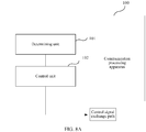
- FIG. 8A is a schematic structural diagram of the communication processing apparatus 100 provided in this embodiment of the present invention.
- the communication processing apparatus 100 includes a determining unit 101 and a control unit 102.
- the determining unit 101 is configured to determine that an FU and an SFU on another integrated main control board different from the integrated main control board need to be controlled.
- the control unit 102 is configured to: when the determining unit 101 determines that the FU and the SFU on the another integrated main control board different from the integrated main control board need to be controlled, control the FU and the SFU on the another integrated main control board different from the integrated main control board by using a control signal exchange path.
- the control signal exchange path is provided between the MCU on the integrated main control board and a hardware forwarding unit on the another integrated main control board different from the integrated main control board, and the hardware forwarding unit includes the FU and the SFU.
- the determining unit 101 may be configured to: detect running statuses of an MCU, the FU, and the SFU integrated on the another integrated main control board; and when detecting that the MCU on the another integrated main control board is in a fault state, and that at least one of the FU or the SFU is in a normal working state, determine, by the determining unit 101, that the FU and the SFU that are integrated on the another integrated main control board and that are in the normal working state need to be controlled.
- control unit 102 may be configured to: control, by using the control signal exchange path, the FU and the SFU on the another integrated main control board different from the integrated main control board to clear original hardware configuration data; and send, by using the control signal exchange path, pre-stored hardware configuration data to the FU and the SFU on the another integrated main control board different from the integrated main control board.
- the pre-stored hardware configuration data is hardware configuration data of the FU and the SFU on the another integrated main control board different from the integrated main control board.
- control unit 102 may alternatively control the FU and the SFU that are integrated on the another integrated main control board and that are in the normal working state by using the control signal exchange path in the following manner, including: obtaining, by using the control signal exchange path, original hardware configuration data of the FU and the SFU that are integrated on the another integrated main control board and that are in the normal working state; performing consistency verification on pre-stored hardware configuration data and the original hardware configuration data; and updating original hardware configuration data different from the pre-stored hardware configuration data with reference to the pre-stored hardware configuration data.
- the pre-stored hardware configuration data is hardware configuration data of the FU and the SFU that are integrated on the another integrated main control board.
- control unit 102 is further configured to: before controlling the FU and the SFU on the another integrated main control board different from the integrated main control board by using the control signal exchange path, configure a selector on the another integrated main control board different from the integrated main control board, to choose to control, by using the control signal exchange path, the FU and the SFU on the another integrated main control board different from the integrated main control board.
- the communication processing apparatus 100 may further include a storage unit 103.
- the storage unit 103 is configured to pre-store, in a form of a mirror table, the hardware configuration data of the FU and the SFU that are on the another integrated main control board.
- the communication processing apparatus 100 provided in this embodiment of the present invention may be configured to perform the communication processing method in the foregoing embodiment, for example, the communication processing processes shown in FIG. 4 to FIG. 7 , and has corresponding functions.
- the communication processing apparatus 100 may be configured to perform the communication processing method in the foregoing embodiment, for example, the communication processing processes shown in FIG. 4 to FIG. 7 , and has corresponding functions.
- the communication processing apparatus 100 that is not described in detail, refer to related descriptions in the method embodiment, and details are not described herein again.
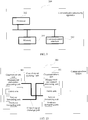
- FIG. 9 is a schematic composition diagram of the communication processing apparatus 200 provided in this embodiment of the present invention.
- the communication processing apparatus 200 includes a bus, a memory 201, a processor 202, and a communications interface 203.
- Program code for executing the solution of the present invention is stored in the memory 201, and is controlled and executed by the processor 202.
- the bus may include a path, and is configured to transfer information between various components of a computer.
- the processor 202 may be a general-purpose central processing unit (CPU), a microprocessor, an application-specific integrated circuit (ASIC), or one or more integrated circuits configured to control execution of a program of the solution of the present invention.
- a computer system includes one or more memories, which may be a read-only memory (ROM) or another type of static storage device that may store static information and instructions, a random access memory (RAM) or another type of dynamic storage device that may store information and instructions, or a magnetic disk memory. These memories are connected to the processor by using the bus.
- the communications interface 203 may be configured to communicate with another device or a communications network by using any apparatus such as a transceiver.
- the memory 201 such as a RAM stores an operating system and a program for executing the solution of the present invention.
- the operating system is a program used to control running of another program and manage system resources.
- the program stored in the memory 201 is used to instruct the processor 202 to perform a communication processing method, including: determining that an FU and an SFU on another integrated main control board need to be controlled; and controlling the FU and the SFU on the another integrated main control board different from the integrated main control board by using a control signal exchange path.
- the communication processing apparatus 200 in this embodiment may be configured to implement all functions in the foregoing method embodiment.
- the communication processing apparatus 200 in this embodiment may be configured to implement all functions in the foregoing method embodiment.
- An embodiment of the present invention further provides a computer storage medium, configured to store a computer software instruction used by the communication processing apparatus, including a related program used to implement the foregoing method embodiment.
- a corresponding communication processing method is performed by executing the stored program.
- FIG. 10 is a schematic composition diagram of the communications system according to this embodiment of the present invention.
- the communications system 300 shown in FIG. 10 includes at least two communications units 301, each communications unit 301 includes an MCU and a hardware forwarding unit, and the hardware forwarding unit includes an FU and an SFU.
- a control signal exchange path is provided between the MCU on each communications unit and a hardware forwarding unit on another communications unit in the at least two communications units.
- An MCU on any one of the at least two communications units controls an FU and an SFU on the another communications unit in the at least two communications units by using the control signal exchange path.
- the communications unit included in the communications system in this embodiment of the present invention may be the integrated main control board in the communications device in the foregoing embodiment of the present invention, and has related functions. Therefore, for a structure and a function of each communications unit in this embodiment of the present invention, refer to related descriptions of the communications device and the communication processing method in the foregoing embodiments. Details are not described herein again.
- the storage medium may be a non-transitory (English: non-transitory) medium, such as a random-access memory, a read-only memory, a flash memory, a hard disk, a solid state drive, a magnetic tape (English: magnetic tape), a floppy disk (English: floppy disk), an optical disc (English: optical disc), or any combination thereof.
- a non-transitory (English: non-transitory) medium such as a random-access memory, a read-only memory, a flash memory, a hard disk, a solid state drive, a magnetic tape (English: magnetic tape), a floppy disk (English: floppy disk), an optical disc (English: optical disc), or any combination thereof.
Landscapes
- Engineering & Computer Science (AREA)
- Theoretical Computer Science (AREA)
- Quality & Reliability (AREA)
- Physics & Mathematics (AREA)
- General Engineering & Computer Science (AREA)
- General Physics & Mathematics (AREA)
- Computer Networks & Wireless Communication (AREA)
- Signal Processing (AREA)
- Data Exchanges In Wide-Area Networks (AREA)
- Hardware Redundancy (AREA)
Applications Claiming Priority (1)
| Application Number | Priority Date | Filing Date | Title |
|---|---|---|---|
| PCT/CN2015/097166 WO2017096621A1 (fr) | 2015-12-11 | 2015-12-11 | Dispositif de communication, procédé de traitement de communication, appareil de traitement de communication et système de communication |
Publications (3)
| Publication Number | Publication Date |
|---|---|
| EP3355480A1 true EP3355480A1 (fr) | 2018-08-01 |
| EP3355480A4 EP3355480A4 (fr) | 2018-11-07 |
| EP3355480B1 EP3355480B1 (fr) | 2020-07-15 |
Family
ID=59012605
Family Applications (1)
| Application Number | Title | Priority Date | Filing Date |
|---|---|---|---|
| EP15910095.7A Active EP3355480B1 (fr) | 2015-12-11 | 2015-12-11 | Dispositif de communication, procédé de traitement de communication, appareil de traitement de communication et système de communication |
Country Status (4)
| Country | Link |
|---|---|
| EP (1) | EP3355480B1 (fr) |
| JP (1) | JP6576556B2 (fr) |
| CN (1) | CN108476036B (fr) |
| WO (1) | WO2017096621A1 (fr) |
Families Citing this family (2)
| Publication number | Priority date | Publication date | Assignee | Title |
|---|---|---|---|---|
| CN112003782B (zh) * | 2020-09-02 | 2022-05-24 | 新华三信息安全技术有限公司 | 一种故障处理方法、装置、网络设备及机器可读存储介质 |
| CN114640653B (zh) * | 2022-03-04 | 2024-09-27 | 新讯数字科技(杭州)有限公司 | 一种视频会议中的流媒体分发系统及方法 |
Family Cites Families (14)
| Publication number | Priority date | Publication date | Assignee | Title |
|---|---|---|---|---|
| US7417947B1 (en) * | 2005-01-05 | 2008-08-26 | Juniper Networks, Inc. | Routing protocol failover between control units within a network router |
| CN100372253C (zh) * | 2005-06-02 | 2008-02-27 | 杭州华三通信技术有限公司 | 双主控系统中业务端口的切换方法及装置 |
| CN100336345C (zh) * | 2005-10-27 | 2007-09-05 | 杭州华三通信技术有限公司 | 双主控网络设备及其主备切换方法 |
| CN100502253C (zh) * | 2006-03-24 | 2009-06-17 | 华为技术有限公司 | 通信设备及主控板和业务板主备倒换的实现方法 |
| CN101710865A (zh) * | 2009-12-23 | 2010-05-19 | 中兴通讯股份有限公司 | 一种网络设备中主备快速倒换的方法和装置 |
| JP5496371B2 (ja) * | 2011-01-25 | 2014-05-21 | アラクサラネットワークス株式会社 | ネットワーク中継システム及びネットワーク中継装置 |
| US9049256B1 (en) * | 2011-03-18 | 2015-06-02 | Juniper Networks, Inc. | Fabric switchover for systems with control plane and fabric plane on same board |
| JP5596637B2 (ja) * | 2011-08-02 | 2014-09-24 | 日本電信電話株式会社 | 障害切替システム、障害切替装置および障害切替方法 |
| WO2013146785A1 (fr) * | 2012-03-28 | 2013-10-03 | 日本電気株式会社 | Système et appareil de communication, appareil de commande, procédé et programme de commande d'appareil de communication |
| EP2839606A4 (fr) * | 2012-04-18 | 2015-08-05 | Ericsson Telefon Ab L M | Système et procédé d'envoi de paquets oam sur des chemins de redondance |
| CN103853623A (zh) * | 2012-11-30 | 2014-06-11 | 华为技术有限公司 | 数据迁移方法及装置 |
| WO2015033726A1 (fr) * | 2013-09-06 | 2015-03-12 | アラクサラネットワークス株式会社 | Dispositif et système de communication |
| CN103490931B (zh) * | 2013-09-25 | 2016-09-07 | 杭州华三通信技术有限公司 | 一种不中断业务升级过程中协议不中断的方法和装置 |
| CN104394018B (zh) * | 2014-11-28 | 2018-05-25 | 上海斐讯数据通信技术有限公司 | 一种通信设备及主控板热备份中主备系统数据在线交换方法 |
-
2015
- 2015-12-11 EP EP15910095.7A patent/EP3355480B1/fr active Active
- 2015-12-11 WO PCT/CN2015/097166 patent/WO2017096621A1/fr not_active Ceased
- 2015-12-11 JP JP2018524473A patent/JP6576556B2/ja active Active
- 2015-12-11 CN CN201580084978.3A patent/CN108476036B/zh active Active
Also Published As
| Publication number | Publication date |
|---|---|
| JP2018533889A (ja) | 2018-11-15 |
| EP3355480A4 (fr) | 2018-11-07 |
| JP6576556B2 (ja) | 2019-09-18 |
| WO2017096621A1 (fr) | 2017-06-15 |
| CN108476036A (zh) | 2018-08-31 |
| EP3355480B1 (fr) | 2020-07-15 |
| CN108476036B (zh) | 2021-01-29 |
Similar Documents
| Publication | Publication Date | Title |
|---|---|---|
| US10938630B2 (en) | Service state transition method and apparatus | |
| CN109861839B (zh) | 业务不中断的虚拟交换机升级方法以及相关设备 | |
| US9934097B2 (en) | Method and apparatus for startup of a central processing unit and a computer system | |
| EP3285168A1 (fr) | Procédé et appareil de tolérance aux catastrophes dans un système de groupe actif-actif | |
| US11947970B2 (en) | Information processing device, moving object, and information processing method | |
| WO2017107656A1 (fr) | Procédé et dispositif d'auto-cicatrisation de défaillance d'élément de réseau virtualisé | |
| CN106502814B (zh) | 一种记录pcie设备错误信息的方法及装置 | |
| EP3879875A1 (fr) | Procédé et dispositif de changement de ressource, appareil, et support de stockage | |
| CN108319492B (zh) | 复位物理机的方法、装置与系统 | |
| CN112732616B (zh) | 一种基于spi控制器的bmc启动方法、装置及设备 | |
| US20200034180A1 (en) | Virtual network system, vim, virtual network control method and recording medium | |
| US9720755B2 (en) | Information processing device | |
| CN106161086B (zh) | 主控板重启的控制方法及装置 | |
| EP3355480B1 (fr) | Dispositif de communication, procédé de traitement de communication, appareil de traitement de communication et système de communication | |
| EP3316518B1 (fr) | Procédé et dispositif de mise à niveau d'un élément de réseau virtuel, et support de stockage informatique | |
| JP2015032301A (ja) | 仮想ホストのバージョンアップ方法、および、ネットワーク装置 | |
| CN110879657B (zh) | 跨版本升级方法、装置及设备、计算机可读存储介质 | |
| CN108234215B (zh) | 一种网关的创建方法、装置、计算机设备及存储介质 | |
| CN107087021B (zh) | 主从服务器确定方法及装置 | |
| CN106685683A (zh) | 管理指示发送、vnf自动伸缩功能的管理方法及装置 | |
| EP3280091A1 (fr) | Procédé, appareil et système d'établissement d'interface entre gestionnaires de fonctions de réseau virtualisé (vfnm) | |
| CN105406989A (zh) | 处理报文的方法、网卡及系统、更新信息的方法及主机 | |
| WO2015192298A1 (fr) | Dispositif de télécommunication et procédé pour mettre à jour un logiciel dans un dispositif de télécommunication | |
| WO2016206399A1 (fr) | Équipement de communication, dispositif et procédé de mise à niveau de version logicielle utilisé dans un équipement de communication | |
| JP6375803B2 (ja) | コマンド実行システム、クライアント装置、サーバ装置及びコマンド実行方法 |
Legal Events
| Date | Code | Title | Description |
|---|---|---|---|
| STAA | Information on the status of an ep patent application or granted ep patent |
Free format text: STATUS: THE INTERNATIONAL PUBLICATION HAS BEEN MADE |
|
| PUAI | Public reference made under article 153(3) epc to a published international application that has entered the european phase |
Free format text: ORIGINAL CODE: 0009012 |
|
| STAA | Information on the status of an ep patent application or granted ep patent |
Free format text: STATUS: REQUEST FOR EXAMINATION WAS MADE |
|
| 17P | Request for examination filed |
Effective date: 20180427 |
|
| AK | Designated contracting states |
Kind code of ref document: A1 Designated state(s): AL AT BE BG CH CY CZ DE DK EE ES FI FR GB GR HR HU IE IS IT LI LT LU LV MC MK MT NL NO PL PT RO RS SE SI SK SM TR |
|
| AX | Request for extension of the european patent |
Extension state: BA ME |
|
| A4 | Supplementary search report drawn up and despatched |
Effective date: 20181010 |
|
| RIC1 | Information provided on ipc code assigned before grant |
Ipc: H04L 12/24 20060101ALI20181004BHEP Ipc: H04B 1/74 20060101AFI20181004BHEP Ipc: H04L 12/939 20130101ALI20181004BHEP |
|
| DAV | Request for validation of the european patent (deleted) | ||
| DAX | Request for extension of the european patent (deleted) | ||
| RIC1 | Information provided on ipc code assigned before grant |
Ipc: H04L 12/939 20130101ALI20191218BHEP Ipc: G06F 11/07 20060101ALI20191218BHEP Ipc: H04B 1/74 20060101AFI20191218BHEP Ipc: H04L 12/24 20060101ALI20191218BHEP Ipc: G06F 11/20 20060101ALI20191218BHEP |
|
| GRAP | Despatch of communication of intention to grant a patent |
Free format text: ORIGINAL CODE: EPIDOSNIGR1 |
|
| STAA | Information on the status of an ep patent application or granted ep patent |
Free format text: STATUS: GRANT OF PATENT IS INTENDED |
|
| INTG | Intention to grant announced |
Effective date: 20200130 |
|
| GRAS | Grant fee paid |
Free format text: ORIGINAL CODE: EPIDOSNIGR3 |
|
| GRAA | (expected) grant |
Free format text: ORIGINAL CODE: 0009210 |
|
| STAA | Information on the status of an ep patent application or granted ep patent |
Free format text: STATUS: THE PATENT HAS BEEN GRANTED |
|
| AK | Designated contracting states |
Kind code of ref document: B1 Designated state(s): AL AT BE BG CH CY CZ DE DK EE ES FI FR GB GR HR HU IE IS IT LI LT LU LV MC MK MT NL NO PL PT RO RS SE SI SK SM TR |
|
| REG | Reference to a national code |
Ref country code: GB Ref legal event code: FG4D Ref country code: CH Ref legal event code: EP |
|
| REG | Reference to a national code |
Ref country code: DE Ref legal event code: R096 Ref document number: 602015055997 Country of ref document: DE |
|
| REG | Reference to a national code |
Ref country code: IE Ref legal event code: FG4D |
|
| REG | Reference to a national code |
Ref country code: AT Ref legal event code: REF Ref document number: 1292118 Country of ref document: AT Kind code of ref document: T Effective date: 20200815 |
|
| REG | Reference to a national code |
Ref country code: LT Ref legal event code: MG4D |
|
| REG | Reference to a national code |
Ref country code: AT Ref legal event code: MK05 Ref document number: 1292118 Country of ref document: AT Kind code of ref document: T Effective date: 20200715 |
|
| REG | Reference to a national code |
Ref country code: NL Ref legal event code: MP Effective date: 20200715 |
|
| PG25 | Lapsed in a contracting state [announced via postgrant information from national office to epo] |
Ref country code: LT Free format text: LAPSE BECAUSE OF FAILURE TO SUBMIT A TRANSLATION OF THE DESCRIPTION OR TO PAY THE FEE WITHIN THE PRESCRIBED TIME-LIMIT Effective date: 20200715 Ref country code: ES Free format text: LAPSE BECAUSE OF FAILURE TO SUBMIT A TRANSLATION OF THE DESCRIPTION OR TO PAY THE FEE WITHIN THE PRESCRIBED TIME-LIMIT Effective date: 20200715 Ref country code: PT Free format text: LAPSE BECAUSE OF FAILURE TO SUBMIT A TRANSLATION OF THE DESCRIPTION OR TO PAY THE FEE WITHIN THE PRESCRIBED TIME-LIMIT Effective date: 20201116 Ref country code: BG Free format text: LAPSE BECAUSE OF FAILURE TO SUBMIT A TRANSLATION OF THE DESCRIPTION OR TO PAY THE FEE WITHIN THE PRESCRIBED TIME-LIMIT Effective date: 20201015 Ref country code: FI Free format text: LAPSE BECAUSE OF FAILURE TO SUBMIT A TRANSLATION OF THE DESCRIPTION OR TO PAY THE FEE WITHIN THE PRESCRIBED TIME-LIMIT Effective date: 20200715 Ref country code: GR Free format text: LAPSE BECAUSE OF FAILURE TO SUBMIT A TRANSLATION OF THE DESCRIPTION OR TO PAY THE FEE WITHIN THE PRESCRIBED TIME-LIMIT Effective date: 20201016 Ref country code: NO Free format text: LAPSE BECAUSE OF FAILURE TO SUBMIT A TRANSLATION OF THE DESCRIPTION OR TO PAY THE FEE WITHIN THE PRESCRIBED TIME-LIMIT Effective date: 20201015 Ref country code: SE Free format text: LAPSE BECAUSE OF FAILURE TO SUBMIT A TRANSLATION OF THE DESCRIPTION OR TO PAY THE FEE WITHIN THE PRESCRIBED TIME-LIMIT Effective date: 20200715 Ref country code: AT Free format text: LAPSE BECAUSE OF FAILURE TO SUBMIT A TRANSLATION OF THE DESCRIPTION OR TO PAY THE FEE WITHIN THE PRESCRIBED TIME-LIMIT Effective date: 20200715 Ref country code: HR Free format text: LAPSE BECAUSE OF FAILURE TO SUBMIT A TRANSLATION OF THE DESCRIPTION OR TO PAY THE FEE WITHIN THE PRESCRIBED TIME-LIMIT Effective date: 20200715 |
|
| PG25 | Lapsed in a contracting state [announced via postgrant information from national office to epo] |
Ref country code: IS Free format text: LAPSE BECAUSE OF FAILURE TO SUBMIT A TRANSLATION OF THE DESCRIPTION OR TO PAY THE FEE WITHIN THE PRESCRIBED TIME-LIMIT Effective date: 20201115 Ref country code: RS Free format text: LAPSE BECAUSE OF FAILURE TO SUBMIT A TRANSLATION OF THE DESCRIPTION OR TO PAY THE FEE WITHIN THE PRESCRIBED TIME-LIMIT Effective date: 20200715 Ref country code: LV Free format text: LAPSE BECAUSE OF FAILURE TO SUBMIT A TRANSLATION OF THE DESCRIPTION OR TO PAY THE FEE WITHIN THE PRESCRIBED TIME-LIMIT Effective date: 20200715 Ref country code: PL Free format text: LAPSE BECAUSE OF FAILURE TO SUBMIT A TRANSLATION OF THE DESCRIPTION OR TO PAY THE FEE WITHIN THE PRESCRIBED TIME-LIMIT Effective date: 20200715 |
|
| PG25 | Lapsed in a contracting state [announced via postgrant information from national office to epo] |
Ref country code: NL Free format text: LAPSE BECAUSE OF FAILURE TO SUBMIT A TRANSLATION OF THE DESCRIPTION OR TO PAY THE FEE WITHIN THE PRESCRIBED TIME-LIMIT Effective date: 20200715 |
|
| REG | Reference to a national code |
Ref country code: DE Ref legal event code: R097 Ref document number: 602015055997 Country of ref document: DE |
|
| PG25 | Lapsed in a contracting state [announced via postgrant information from national office to epo] |
Ref country code: EE Free format text: LAPSE BECAUSE OF FAILURE TO SUBMIT A TRANSLATION OF THE DESCRIPTION OR TO PAY THE FEE WITHIN THE PRESCRIBED TIME-LIMIT Effective date: 20200715 Ref country code: SM Free format text: LAPSE BECAUSE OF FAILURE TO SUBMIT A TRANSLATION OF THE DESCRIPTION OR TO PAY THE FEE WITHIN THE PRESCRIBED TIME-LIMIT Effective date: 20200715 Ref country code: RO Free format text: LAPSE BECAUSE OF FAILURE TO SUBMIT A TRANSLATION OF THE DESCRIPTION OR TO PAY THE FEE WITHIN THE PRESCRIBED TIME-LIMIT Effective date: 20200715 Ref country code: DK Free format text: LAPSE BECAUSE OF FAILURE TO SUBMIT A TRANSLATION OF THE DESCRIPTION OR TO PAY THE FEE WITHIN THE PRESCRIBED TIME-LIMIT Effective date: 20200715 Ref country code: CZ Free format text: LAPSE BECAUSE OF FAILURE TO SUBMIT A TRANSLATION OF THE DESCRIPTION OR TO PAY THE FEE WITHIN THE PRESCRIBED TIME-LIMIT Effective date: 20200715 |
|
| PLBE | No opposition filed within time limit |
Free format text: ORIGINAL CODE: 0009261 |
|
| STAA | Information on the status of an ep patent application or granted ep patent |
Free format text: STATUS: NO OPPOSITION FILED WITHIN TIME LIMIT |
|
| PG25 | Lapsed in a contracting state [announced via postgrant information from national office to epo] |
Ref country code: AL Free format text: LAPSE BECAUSE OF FAILURE TO SUBMIT A TRANSLATION OF THE DESCRIPTION OR TO PAY THE FEE WITHIN THE PRESCRIBED TIME-LIMIT Effective date: 20200715 |
|
| 26N | No opposition filed |
Effective date: 20210416 |
|
| PG25 | Lapsed in a contracting state [announced via postgrant information from national office to epo] |
Ref country code: SK Free format text: LAPSE BECAUSE OF FAILURE TO SUBMIT A TRANSLATION OF THE DESCRIPTION OR TO PAY THE FEE WITHIN THE PRESCRIBED TIME-LIMIT Effective date: 20200715 |
|
| PG25 | Lapsed in a contracting state [announced via postgrant information from national office to epo] |
Ref country code: SI Free format text: LAPSE BECAUSE OF FAILURE TO SUBMIT A TRANSLATION OF THE DESCRIPTION OR TO PAY THE FEE WITHIN THE PRESCRIBED TIME-LIMIT Effective date: 20200715 Ref country code: MC Free format text: LAPSE BECAUSE OF FAILURE TO SUBMIT A TRANSLATION OF THE DESCRIPTION OR TO PAY THE FEE WITHIN THE PRESCRIBED TIME-LIMIT Effective date: 20200715 |
|
| REG | Reference to a national code |
Ref country code: BE Ref legal event code: MM Effective date: 20201231 |
|
| PG25 | Lapsed in a contracting state [announced via postgrant information from national office to epo] |
Ref country code: IE Free format text: LAPSE BECAUSE OF NON-PAYMENT OF DUE FEES Effective date: 20201211 Ref country code: LU Free format text: LAPSE BECAUSE OF NON-PAYMENT OF DUE FEES Effective date: 20201211 |
|
| PG25 | Lapsed in a contracting state [announced via postgrant information from national office to epo] |
Ref country code: TR Free format text: LAPSE BECAUSE OF FAILURE TO SUBMIT A TRANSLATION OF THE DESCRIPTION OR TO PAY THE FEE WITHIN THE PRESCRIBED TIME-LIMIT Effective date: 20200715 Ref country code: MT Free format text: LAPSE BECAUSE OF FAILURE TO SUBMIT A TRANSLATION OF THE DESCRIPTION OR TO PAY THE FEE WITHIN THE PRESCRIBED TIME-LIMIT Effective date: 20200715 Ref country code: CY Free format text: LAPSE BECAUSE OF FAILURE TO SUBMIT A TRANSLATION OF THE DESCRIPTION OR TO PAY THE FEE WITHIN THE PRESCRIBED TIME-LIMIT Effective date: 20200715 |
|
| PG25 | Lapsed in a contracting state [announced via postgrant information from national office to epo] |
Ref country code: MK Free format text: LAPSE BECAUSE OF FAILURE TO SUBMIT A TRANSLATION OF THE DESCRIPTION OR TO PAY THE FEE WITHIN THE PRESCRIBED TIME-LIMIT Effective date: 20200715 |
|
| PG25 | Lapsed in a contracting state [announced via postgrant information from national office to epo] |
Ref country code: BE Free format text: LAPSE BECAUSE OF NON-PAYMENT OF DUE FEES Effective date: 20201231 |
|
| PGFP | Annual fee paid to national office [announced via postgrant information from national office to epo] |
Ref country code: IT Payment date: 20241112 Year of fee payment: 10 |
|
| PGFP | Annual fee paid to national office [announced via postgrant information from national office to epo] |
Ref country code: CH Payment date: 20250101 Year of fee payment: 10 |
|
| PGFP | Annual fee paid to national office [announced via postgrant information from national office to epo] |
Ref country code: DE Payment date: 20251104 Year of fee payment: 11 |
|
| PGFP | Annual fee paid to national office [announced via postgrant information from national office to epo] |
Ref country code: GB Payment date: 20251030 Year of fee payment: 11 |
|
| PGFP | Annual fee paid to national office [announced via postgrant information from national office to epo] |
Ref country code: FR Payment date: 20251110 Year of fee payment: 11 |