EP3358357A1 - Capteur d'inertie - Google Patents
Capteur d'inertie Download PDFInfo
- Publication number
- EP3358357A1 EP3358357A1 EP16850874.5A EP16850874A EP3358357A1 EP 3358357 A1 EP3358357 A1 EP 3358357A1 EP 16850874 A EP16850874 A EP 16850874A EP 3358357 A1 EP3358357 A1 EP 3358357A1
- Authority
- EP
- European Patent Office
- Prior art keywords
- electrode
- detector
- weight
- angular velocity
- acceleration
- Prior art date
- Legal status (The legal status is an assumption and is not a legal conclusion. Google has not performed a legal analysis and makes no representation as to the accuracy of the status listed.)
- Withdrawn
Links
Images







Classifications
-
- B—PERFORMING OPERATIONS; TRANSPORTING
- B81—MICROSTRUCTURAL TECHNOLOGY
- B81B—MICROSTRUCTURAL DEVICES OR SYSTEMS, e.g. MICROMECHANICAL DEVICES
- B81B7/00—Microstructural systems ; Auxiliary parts of microstructural devices or systems
- B81B7/02—Microstructural systems ; Auxiliary parts of microstructural devices or systems containing distinct electrical or optical devices of particular relevance for their function, e.g. microelectro-mechanical systems [MEMS]
-
- G—PHYSICS
- G01—MEASURING; TESTING
- G01C—MEASURING DISTANCES, LEVELS OR BEARINGS; SURVEYING; NAVIGATION; GYROSCOPIC INSTRUMENTS; PHOTOGRAMMETRY OR VIDEOGRAMMETRY
- G01C19/00—Gyroscopes; Turn-sensitive devices using vibrating masses; Turn-sensitive devices without moving masses; Measuring angular rate using gyroscopic effects
- G01C19/56—Turn-sensitive devices using vibrating masses, e.g. vibratory angular rate sensors based on Coriolis forces
- G01C19/5719—Turn-sensitive devices using vibrating masses, e.g. vibratory angular rate sensors based on Coriolis forces using planar vibrating masses driven in a translation vibration along an axis
- G01C19/5733—Structural details or topology
- G01C19/574—Structural details or topology the devices having two sensing masses in anti-phase motion
- G01C19/5747—Structural details or topology the devices having two sensing masses in anti-phase motion each sensing mass being connected to a driving mass, e.g. driving frames
-
- G—PHYSICS
- G01—MEASURING; TESTING
- G01C—MEASURING DISTANCES, LEVELS OR BEARINGS; SURVEYING; NAVIGATION; GYROSCOPIC INSTRUMENTS; PHOTOGRAMMETRY OR VIDEOGRAMMETRY
- G01C19/00—Gyroscopes; Turn-sensitive devices using vibrating masses; Turn-sensitive devices without moving masses; Measuring angular rate using gyroscopic effects
- G01C19/56—Turn-sensitive devices using vibrating masses, e.g. vibratory angular rate sensors based on Coriolis forces
- G01C19/5783—Mountings or housings not specific to any of the devices covered by groups G01C19/5607 - G01C19/5719
-
- G—PHYSICS
- G01—MEASURING; TESTING
- G01D—MEASURING NOT SPECIALLY ADAPTED FOR A SPECIFIC VARIABLE; ARRANGEMENTS FOR MEASURING TWO OR MORE VARIABLES NOT COVERED IN A SINGLE OTHER SUBCLASS; TARIFF METERING APPARATUS; MEASURING OR TESTING NOT OTHERWISE PROVIDED FOR
- G01D21/00—Measuring or testing not otherwise provided for
- G01D21/02—Measuring two or more variables by means not covered by a single other subclass
-
- G—PHYSICS
- G01—MEASURING; TESTING
- G01L—MEASURING FORCE, STRESS, TORQUE, WORK, MECHANICAL POWER, MECHANICAL EFFICIENCY, OR FLUID PRESSURE
- G01L9/00—Measuring steady of quasi-steady pressure of fluid or fluent solid material by electric or magnetic pressure-sensitive elements; Transmitting or indicating the displacement of mechanical pressure-sensitive elements, used to measure the steady or quasi-steady pressure of a fluid or fluent solid material, by electric or magnetic means
- G01L9/0041—Transmitting or indicating the displacement of flexible diaphragms
- G01L9/0051—Transmitting or indicating the displacement of flexible diaphragms using variations in ohmic resistance
- G01L9/0052—Transmitting or indicating the displacement of flexible diaphragms using variations in ohmic resistance of piezoresistive elements
-
- G—PHYSICS
- G01—MEASURING; TESTING
- G01L—MEASURING FORCE, STRESS, TORQUE, WORK, MECHANICAL POWER, MECHANICAL EFFICIENCY, OR FLUID PRESSURE
- G01L9/00—Measuring steady of quasi-steady pressure of fluid or fluent solid material by electric or magnetic pressure-sensitive elements; Transmitting or indicating the displacement of mechanical pressure-sensitive elements, used to measure the steady or quasi-steady pressure of a fluid or fluent solid material, by electric or magnetic means
- G01L9/12—Measuring steady of quasi-steady pressure of fluid or fluent solid material by electric or magnetic pressure-sensitive elements; Transmitting or indicating the displacement of mechanical pressure-sensitive elements, used to measure the steady or quasi-steady pressure of a fluid or fluent solid material, by electric or magnetic means by making use of variations in capacitance, i.e. electric circuits therefor
-
- G—PHYSICS
- G01—MEASURING; TESTING
- G01P—MEASURING LINEAR OR ANGULAR SPEED, ACCELERATION, DECELERATION, OR SHOCK; INDICATING PRESENCE, ABSENCE, OR DIRECTION, OF MOVEMENT
- G01P15/00—Measuring acceleration; Measuring deceleration; Measuring shock, i.e. sudden change of acceleration
- G01P15/02—Measuring acceleration; Measuring deceleration; Measuring shock, i.e. sudden change of acceleration by making use of inertia forces using solid seismic masses
- G01P15/08—Measuring acceleration; Measuring deceleration; Measuring shock, i.e. sudden change of acceleration by making use of inertia forces using solid seismic masses with conversion into electric or magnetic values
- G01P15/0802—Details
-
- G—PHYSICS
- G01—MEASURING; TESTING
- G01P—MEASURING LINEAR OR ANGULAR SPEED, ACCELERATION, DECELERATION, OR SHOCK; INDICATING PRESENCE, ABSENCE, OR DIRECTION, OF MOVEMENT
- G01P15/00—Measuring acceleration; Measuring deceleration; Measuring shock, i.e. sudden change of acceleration
- G01P15/02—Measuring acceleration; Measuring deceleration; Measuring shock, i.e. sudden change of acceleration by making use of inertia forces using solid seismic masses
- G01P15/08—Measuring acceleration; Measuring deceleration; Measuring shock, i.e. sudden change of acceleration by making use of inertia forces using solid seismic masses with conversion into electric or magnetic values
- G01P15/125—Measuring acceleration; Measuring deceleration; Measuring shock, i.e. sudden change of acceleration by making use of inertia forces using solid seismic masses with conversion into electric or magnetic values by capacitive pick-up
-
- G—PHYSICS
- G01—MEASURING; TESTING
- G01P—MEASURING LINEAR OR ANGULAR SPEED, ACCELERATION, DECELERATION, OR SHOCK; INDICATING PRESENCE, ABSENCE, OR DIRECTION, OF MOVEMENT
- G01P15/00—Measuring acceleration; Measuring deceleration; Measuring shock, i.e. sudden change of acceleration
- G01P15/18—Measuring acceleration; Measuring deceleration; Measuring shock, i.e. sudden change of acceleration in two or more dimensions
-
- B—PERFORMING OPERATIONS; TRANSPORTING
- B81—MICROSTRUCTURAL TECHNOLOGY
- B81B—MICROSTRUCTURAL DEVICES OR SYSTEMS, e.g. MICROMECHANICAL DEVICES
- B81B2201/00—Specific applications of microelectromechanical systems
- B81B2201/02—Sensors
- B81B2201/0228—Inertial sensors
- B81B2201/0235—Accelerometers
-
- B—PERFORMING OPERATIONS; TRANSPORTING
- B81—MICROSTRUCTURAL TECHNOLOGY
- B81B—MICROSTRUCTURAL DEVICES OR SYSTEMS, e.g. MICROMECHANICAL DEVICES
- B81B2201/00—Specific applications of microelectromechanical systems
- B81B2201/02—Sensors
- B81B2201/0228—Inertial sensors
- B81B2201/0242—Gyroscopes
-
- B—PERFORMING OPERATIONS; TRANSPORTING
- B81—MICROSTRUCTURAL TECHNOLOGY
- B81B—MICROSTRUCTURAL DEVICES OR SYSTEMS, e.g. MICROMECHANICAL DEVICES
- B81B2201/00—Specific applications of microelectromechanical systems
- B81B2201/02—Sensors
- B81B2201/0264—Pressure sensors
-
- B—PERFORMING OPERATIONS; TRANSPORTING
- B81—MICROSTRUCTURAL TECHNOLOGY
- B81B—MICROSTRUCTURAL DEVICES OR SYSTEMS, e.g. MICROMECHANICAL DEVICES
- B81B2203/00—Basic microelectromechanical structures
- B81B2203/01—Suspended structures, i.e. structures allowing a movement
- B81B2203/0109—Bridges
-
- B—PERFORMING OPERATIONS; TRANSPORTING
- B81—MICROSTRUCTURAL TECHNOLOGY
- B81B—MICROSTRUCTURAL DEVICES OR SYSTEMS, e.g. MICROMECHANICAL DEVICES
- B81B2203/00—Basic microelectromechanical structures
- B81B2203/04—Electrodes
-
- B—PERFORMING OPERATIONS; TRANSPORTING
- B81—MICROSTRUCTURAL TECHNOLOGY
- B81B—MICROSTRUCTURAL DEVICES OR SYSTEMS, e.g. MICROMECHANICAL DEVICES
- B81B2203/00—Basic microelectromechanical structures
- B81B2203/05—Type of movement
- B81B2203/051—Translation according to an axis parallel to the substrate
-
- B—PERFORMING OPERATIONS; TRANSPORTING
- B81—MICROSTRUCTURAL TECHNOLOGY
- B81B—MICROSTRUCTURAL DEVICES OR SYSTEMS, e.g. MICROMECHANICAL DEVICES
- B81B2207/00—Microstructural systems or auxiliary parts thereof
- B81B2207/01—Microstructural systems or auxiliary parts thereof comprising a micromechanical device connected to control or processing electronics, i.e. Smart-MEMS
- B81B2207/015—Microstructural systems or auxiliary parts thereof comprising a micromechanical device connected to control or processing electronics, i.e. Smart-MEMS the micromechanical device and the control or processing electronics being integrated on the same substrate
-
- B—PERFORMING OPERATIONS; TRANSPORTING
- B81—MICROSTRUCTURAL TECHNOLOGY
- B81B—MICROSTRUCTURAL DEVICES OR SYSTEMS, e.g. MICROMECHANICAL DEVICES
- B81B2207/00—Microstructural systems or auxiliary parts thereof
- B81B2207/07—Interconnects
-
- G—PHYSICS
- G01—MEASURING; TESTING
- G01P—MEASURING LINEAR OR ANGULAR SPEED, ACCELERATION, DECELERATION, OR SHOCK; INDICATING PRESENCE, ABSENCE, OR DIRECTION, OF MOVEMENT
- G01P1/00—Details of instruments
- G01P1/02—Housings
- G01P1/023—Housings for acceleration measuring devices
-
- G—PHYSICS
- G01—MEASURING; TESTING
- G01P—MEASURING LINEAR OR ANGULAR SPEED, ACCELERATION, DECELERATION, OR SHOCK; INDICATING PRESENCE, ABSENCE, OR DIRECTION, OF MOVEMENT
- G01P15/00—Measuring acceleration; Measuring deceleration; Measuring shock, i.e. sudden change of acceleration
- G01P15/02—Measuring acceleration; Measuring deceleration; Measuring shock, i.e. sudden change of acceleration by making use of inertia forces using solid seismic masses
- G01P15/08—Measuring acceleration; Measuring deceleration; Measuring shock, i.e. sudden change of acceleration by making use of inertia forces using solid seismic masses with conversion into electric or magnetic values
- G01P2015/0805—Measuring acceleration; Measuring deceleration; Measuring shock, i.e. sudden change of acceleration by making use of inertia forces using solid seismic masses with conversion into electric or magnetic values being provided with a particular type of spring-mass-system for defining the displacement of a seismic mass due to an external acceleration
- G01P2015/0808—Measuring acceleration; Measuring deceleration; Measuring shock, i.e. sudden change of acceleration by making use of inertia forces using solid seismic masses with conversion into electric or magnetic values being provided with a particular type of spring-mass-system for defining the displacement of a seismic mass due to an external acceleration for defining in-plane movement of the mass, i.e. movement of the mass in the plane of the substrate
- G01P2015/0811—Measuring acceleration; Measuring deceleration; Measuring shock, i.e. sudden change of acceleration by making use of inertia forces using solid seismic masses with conversion into electric or magnetic values being provided with a particular type of spring-mass-system for defining the displacement of a seismic mass due to an external acceleration for defining in-plane movement of the mass, i.e. movement of the mass in the plane of the substrate for one single degree of freedom of movement of the mass
- G01P2015/0814—Measuring acceleration; Measuring deceleration; Measuring shock, i.e. sudden change of acceleration by making use of inertia forces using solid seismic masses with conversion into electric or magnetic values being provided with a particular type of spring-mass-system for defining the displacement of a seismic mass due to an external acceleration for defining in-plane movement of the mass, i.e. movement of the mass in the plane of the substrate for one single degree of freedom of movement of the mass for translational movement of the mass, e.g. shuttle type
Definitions
- the present invention relates to an inertial force sensor, and more particularly to an acceleration sensor and an angular velocity sensor for measuring a motion state of a moving object such as a vehicle, an airplane, a robot, a mobile phone, a video camera.
- MEMS microelectromechanical systems
- this type of inertial force sensor is formed by processing a semiconductor substrate such as silicon, a glass substrate, or the like, using an MEMS fabrication process such as etching, in which air-tightly sealed voids are formed by bonding the substrate with another substrate under constant atmosphere and pressure environment.
- PTL 1 describes an inertial force sensor including an acceleration detector and an angular velocity detector.
- the acceleration detector includes a movable mechanical component that is a movable body formed with weights, beams, or the like. When the acceleration is applied, the movable body is displaced. Acceleration is detected by detecting a displacement amount of the movable body.
- the angular velocity detector includes a movable mechanical component that is a vibrating body and applying angular velocity to a state in which the vibrating body drives at a certain frequency generates a Coriolis force. This Coriolis force causes the vibrating body to be displaced. The angular velocity is detected by detecting a displacement amount of the vibrating body by this Coriolis force.
- the acceleration detector and the angular velocity detector are installed on a same substrate.
- the acceleration detector and the angular velocity detector have mutually different performance requirements such as the detection sensitivity and the frequency response, and thus, the natural frequency, the electrode dimensions, or the like, for determining the structure of the detector are also different from each other.
- ⁇ , w, l, and E are the following numerical values.
- a natural frequency f1 of the acceleration detector is about 1 kHz to 3 kHz, while a natural frequency f2 of the angular velocity detector is about 15 kHz to 25 kHz, leading to a difference between them in some cases.
- a thickness h of the substrate is common to the two detectors.
- variation in fabricated shapes can be more equalized by also using a common beam width w. Accordingly, in order to obtain the mutually different natural frequencies f1 and f2, the area S and the length 1 of the beam are to be individually changed.
- m 21 and m 22 are the following numerical values.
- v is the following numerical value. v: velocity at drive of weight m 2
- an inertial force sensor according to the present invention includes a layer in which a detector is formed and that the layer has a laminated structure in which two or more layers are laminated.
- the thickness h can be set to an arbitrary thickness in each of the detectors.
- an inertial force sensor includes a layer in which a detector is formed, and the layer is a laminated structure in which two or more layers are laminated. According to the present invention, since the detectors are formed in lamination, it is possible to achieve downsizing compared with a sensor in which detectors are arranged on a plane.
- the inertial force sensor is characterized in that at least one pair of detectors is arranged such that the movable body and the electrode are formed in mutually different layers.
- the electrode in a case where the movable body moves in a direction perpendicular to a plane and this movement is to be detected, the electrode is installed at a position facing the plane of the movable body, that is, in another layer.
- the detector in which the movable body and the electrode are formed in mutually different layers is configured such that the electrode is formed in a same layer in which the movable body of another detector is formed. This makes it possible to reduce the height of the sensor chip because there is no need to provide another layer for the electrode.
- the inertial force sensor is characterized to include two sets of the at least one pair of detectors being arranged in an array.
- the present invention for example, by arranging, in the array, the individual detectors in a direction orthogonal to each other on a plane, it is possible to detect an inertial force in the two-dimensional direction.
- the individual detectors for example, by arranging the individual detectors in a same direction on the plane in the array, it is possible to detect a positional deviation between the individual detectors, detect warping and bending occurring in the sensor chip forming the array, and by correcting the warping and bending by an external circuit, it is possible to enhance detection accuracy of the sensor.
- the number or the like of the components is not limited to a particular number but rather may be a number equal to or more/less than the particular number, except for the cases where explicitly stated, apparently limited to the particular number in principle, or the like.
- components (including element steps, or the like) in the following embodiment are not necessarily indispensable, except for the cases where explicitly stated, considered apparently indispensable in principle, or the like.
- FIG. 1 is an overall view of a sensor chip 10 according to a first embodiment of the present invention.
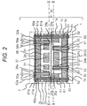
- FIG. 2 is a cross sectional view taken along line I-I in FIG. 1 .
- FIG. 3 is a plan view illustrating a II-II cross section of FIG. 2 .
- FIG. 4 is a plan view illustrating a III-III cross section of FIG. 2 .
- FIG. 5 illustrates a modification of FIG. 2 .
- FIG. 6 is a principle diagram of acceleration signal detection.
- FIG. 7 is a principle diagram of an angular velocity detection signal.
- the sensor chip 10 is constituted with an acceleration detector 20 configured to detect acceleration in the y-axis direction and a detector 30 configured to detect an angular velocity about the z-axis.
- the acceleration detector 20 is formed in a first laminate 1
- the angular velocity detector 30 is formed in a second laminate 2.
- the first laminate 1 and the second laminate 2 are laminated as illustrated in FIG. 2 , and a signal of the acceleration detector 20 and a signal of the angular velocity detector 30 are extracted on a same side in order to facilitate connection to an external circuit to be described below.
- the first laminate 1 has a configuration including a first substrate 1a consisting of mono-crystalline silicon, a second substrate 1b consisting of mono-crystalline silicon in a similar manner, and an oxide film 1c, in which the first substrate 1a and the second substrate 1b are laminated so as to sandwich the oxide film 1c therebetween.
- the laminate 1 may also use a substrate obtained by first forming an insulating film serving as the oxide film 1c on a substrate of silicon and glass bonded with each other, or on a silicon substrate serving as the second substrate 1b, and then forming on an upper portion thereof a conductive film such as a polysilicon film serving as the first substrate 1a.
- the laminate 1 is processed by photolithography and deep reactive ion etching (DRIE), thereby forming the acceleration detector 20.
- DRIE deep reactive ion etching
- the acceleration detector 20 is formed on the first substrate 1a.
- the acceleration detector 20 includes a weight 21, fixed portions 23a, 23b, 23c, and 23d supported and fixed to the second substrate 1b via the oxide film 1c, and beams 22a, 22b, 22c, and 22d joined to the fixed portions and movably supporting the weight 21 in a movable (Y) direction (described below).
- the weight 21 is suspended from the beam and a portion around the weight 21 is in a hollow state surrounded by cavity 29 in order to enable the weight 21 to be movable.
- electrodes 24a and 24b for forming capacitance with the weight 21, and electrodes 25a, 25b, and 26a for exchanging signals with an external circuit.
- the electrodes 25a, 25b, and 26a are configured such that the electrode 25a corresponds to the electrode 24a, the electrode 25b to the electrode 24b, and the electrode 26a to the weight 21.
- a penetrating electrode 50 is formed so as to penetrate the second substrate 1b, the oxide film 1c, and an insulating film 1d that insulates the electrode 52 described below.
- the penetrating electrode 50 is connected to the electrode 52.
- the outer periphery of the penetrating electrode 50 is covered with an insulating film 51 in order to electrically insulate from the substrate through which the penetrating electrode 50 penetrates.
- the inside of the penetrating electrode 50 is formed by embedding a conductive material such as polysilicon or metal.
- a penetrating electrode 60 penetrating the first substrate 1a, the second substrate 1b, the oxide film 1c, and the insulating film 1d, and connection to the electrode 62 is performed via the penetrating electrode 60.
- the outer periphery of the penetrating electrode 60 is covered with an insulating film 61, and the inside is formed of a conductive material such as polysilicon or metal.
- the mass of the weight 21 is defined, as m1 and the sum of spring constants of the beams 22a, 22b, 22c, and 22d in the movable (y) direction is defined as k 1 , as mainly illustrated in FIG. 3 .
- k 1 the sum of spring constants of the beams 22a, 22b, 22c, and 22d in the movable (y) direction.
- a distance between the weight 21 and each of the electrodes 24a and 24b varies, leading to a change in the capacitance of the weight 21 and the electrode 24a on the left side in a decreasing direction and leading to a change in the capacitance of the weight 21 and the electrode 24b on the right side in an increasing direction.
- the distance between the weight 21 and the electrode 24a on the left side increases, leading to a decrease in the capacitance, and at this time, the distance between the weight 21 and the electrode 24b on the right side decreases, leading to an increase in the capacitance.
- This change in the capacitance is output to and processed in the external integrated circuit 100.
- a carrier wave 101 for detecting the capacitance from the integrated circuit 100 formed on a semiconductor chip 3 is applied to the electrode 25a connected to the electrode 24a or to the electrode 25b connected to the electrode 24b, illustrated in FIG. 3 .
- This causes a capacitance change signal to be output from .the electrode 26a connected to the fixed portion 23a joined to the weight 21 illustrated in FIG. 3 via the beam 22a. That is, a signal of capacitance change from the acceleration detector 20 is input to a CV converter 102.
- the carrier wave 101 may be applied so as to have opposite phased waveforms between the electrode 25a and the electrode 25b.
- the signal of the capacitance change from the acceleration detector 20 can be input to the CV converter 102 by differential input. This makes it possible to increase the acceleration detection sensitivity.
- the capacitance change is converted into a voltage signal, and thereafter, the voltage signal is output to a synchronous detector 103.
- the synchronous detector 103 extracts solely a necessary signal component, and finally outputs an acceleration signal 104 in the form of voltage.
- the displacement amount y 1 of the weight 24 is proportional to the applied acceleration when the mass m 1 of the movable body and the total k 1 of the spring constants of the beams 22a, 22b, 22c, and 22d are constant. Accordingly, the applied acceleration can be detected by monitoring an output voltage (acceleration signal) proportional to the displacement amount y 1 .
- the acceleration sensor according to the first embodiment operates as described above.
- the acceleration in the x-axis direction is detected by arranging the acceleration detector 20 to be rotated by 90 degrees about the z-axis.
- an acceleration detector 20a adjacent to the acceleration detector 20 and rotated by 90 degrees about the z-axis with respect to the acceleration detector 20, it is possible to detect acceleration of two axes in the x-axis direction and the y-axis direction in the first laminate 1.
- the angular velocity detector 30 according to the present embodiment is formed by the second laminate 2, similarly to the first laminate 1.
- the angular velocity detector 30 is formed on a first substrate 2a constituting the second laminate 2.
- the angular velocity detector 30 includes: fixed portions 33a, 33b, 33c, and 33d supported and fixed to a second substrate 2b via an oxide film 2c; first beams 32a, 32b, 32c, and 32d respectively joined to the fixed portions and each movably supporting a first weight 31 described below; the first weight 31 suspended from the beams and movable in the movable (X) direction; and electrodes 34a and 34b configured to form capacitances with the weight 31 in order to drive the first weight 31.
- the angular velocity detector 30 further includes second beams 38a, 38b, 38c and 38d configured to join a second weight 37 to the first weight 31 and movably supporting the second weight 37 in a direction (Y) orthogonal to the first weight 31; the second weight 37 movable in the orthogonal (y) direction with respect to the first weight 31 by application of angular velocity; and electrodes 39a and 39b that form capacitance with the second weight 37 in order to detect a displacement amount of the second weight 37 at application of angular velocity as a change in capacitance.
- the angular velocity detector 30 further includes an electrode 35a for the electrode 34a, an electrode 35b for the electrode 34b, an electrode 36a for the second weight 37, an electrode 40a for the electrode 39a, and 40b for the electrode 39b.
- a penetrating electrode 50a that penetrates the second substrate 2b, the oxide film 2c, and an insulating film 2d for insulating the electrode 52a described below is formed, and the penetrating electrode 50a is connected to the electrode 52a.
- the outer periphery of the penetrating electrode 50a is covered with the insulating film 51a, and the inside is formed of a conductive material such as polysilicon or metal.
- the electrode 52a is extended in a planar direction, and similarly to the penetrating electrode 60 formed in the acceleration detector 20, a penetrating electrode 60a penetrating the first substrate 2a, the second substrate 2b, the oxide film 2c, and the insulating film 2d is formed and connected to the electrode 52a.
- the penetrating electrode 60a by arranging the penetrating electrode 60a at a position to be electrically connected to the penetrating electrode 60, the signal of the electrode 52a is connected to the electrode 62 arranged on the same side as the electrode 52.
- the outer periphery of the penetrating electrode 60a is covered with an insulating film 61a, and the inside is formed of a conductive material such as polysilicon or metal.
- an AC voltage of the frequency f is applied to the first electrodes 34a and 34b, so as to generate electrostatic force between the first weight 31 and the first electrodes 34a and 34b, thereby causing the first weight 31 to vibrate in the x-axis direction.
- the AC voltage is generated by an oscillator 205 provided, in an external integrated circuit 200.
- an amplifier 206 may be interposed, in order to obtain a predetermined voltage.
- the second weight 37 vibrates in the y-axis direction by the Coriolis force Fc expressed by Formula (6), and the capacitance between the second weight 37 and the second electrodes 39a and 39b changes. By detecting this capacitance change, it is possible to detect the angular velocity ⁇ about the z-axis.
- This change in the capacitance is output to and processed in the external integrated circuit 200.
- a carrier wave 201 for detecting the capacitance from the integrated circuit 200 formed on a semiconductor chip 3a is applied to the electrode 40a connected to the electrode 39a or to the electrode 40b connected to the electrode 39b, illustrated in FIG. 4 .
- the carrier wave 201 may be applied so as to have opposite phased waveforms between the electrode 40a and the electrode 40b.
- the signal of the capacitance change from the angular velocity detector 30 can be input to the CV converter 202 by differential input. This makes it possible to increase angular velocity detection sensitivity.
- the capacitance change is converted into a voltage signal, and thereafter, the voltage signal is output to a synchronous detector 203.
- the synchronous detector 203 extracts solely a necessary signal component and finally outputs an angular velocity signal 204 in the form of voltage.
- the voltage applied to the electrodes 39a and 39b may be servo-controlled such that the capacitance change between the weight 37 and the electrodes 39a, 39b, that is, the displacement amount in the y-axis direction of the weight 37 becomes zero, and the Coriolis force Fc may be obtained from the applied voltage.
- FIG. 8 it is possible to provide a structure in which two angular velocity detectors 30 are arranged side by side, and an angular velocity detector 30q1 on the left side and an angular velocity detector 30q2 on the right side are provided with being mutually connected via a third beam 41 formed on the first substrate 2a.
- the detection signal of the angular velocity can be detected with high sensitivity by obtaining a sum of a second weight 37q1 of the left side and a second weight 37q2 on the right side, leading to an advantage of capability of suppressing the vibration of a transducer from leaking to the outside.
- the angular velocity detector 30 formed in the second laminate 2 is the description of the angular velocity detector 30 formed in the second laminate 2 according to the present embodiment. Alternatively, however, it is allowable to form an acceleration detector 20b in the second laminate 2, similarly to the acceleration detector 20.
- the acceleration detector 20b may be arranged to be rotated by 90 degrees about the z-axis with respect to the acceleration detector 20, whereby the acceleration detector 20 detects the acceleration in the y-axis direction, while the acceleration detector 20b detects the acceleration about the x-axis, enabling the sensor chip 10 to be a biaxial acceleration sensor that detects acceleration in the x-axis and the y-axis directions.
- the acceleration detector 20b is arranged in the same direction as the acceleration detector 20, while by changing the dimensions of the beam and the weight, and the thickness of the first substrate 2a so as to change the spring constant k 1 and the mass m 1 expressed in Formula (7) to different values, it is possible to change the acceleration detection range.
- the sensor chip 10 can be a uniaxial acceleration sensor with a wider detection range without deteriorating detection accuracy.
- the first laminate 1 according to the present embodiment may include an angular velocity detector 30a similarly to the angular velocity detector 30.
- an angular velocity detector 30a similarly to the angular velocity detector 30.
- the integrated circuit 100 and the integrated circuit 200 are formed on the same semiconductor chip 3, it is possible to downsize the semiconductor chip.
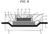
- the sensor chip 10 constituted as described above is assembled in a chip package 4 as illustrated in FIG. 9 .
- the sensor chip 10 is mounted on the semiconductor chip 3 via an adhesive 70 with an insulating film 2d side surface of the second laminate 2 facing the semiconductor chip 3, while the electrodes 52 and 62 of the sensor chip 10 are electrically connected to the semiconductor chip 3 via first wire bonding 71.
- the semiconductor chip 3 is mounted on a lead frame 72 via an adhesive 73, and the semiconductor chip 3 and the lead frame 72 are electrically connected via the second wire bonding 74. Then, these are sealed with resin 75, thereby forming the chip package 4.
- FIG. 10 illustrates as a chip package 4a as a modification of the chip package 4 illustrated in FIG. 9 .
- a semiconductor chip 3b includes electrodes 81 and 82 connected to the electrodes 52 and 62 on the sensor chip 10 at positions facing the electrodes 52 and 62, respectively. Portions between the electrodes 52 and 81 and between the electrodes 62 and 82 are electrically connected via a conductive material 76 such as a solder bump, thereby bonding the sensor chip 10 and the semiconductor chip 3b to each other.
- an adhesive 73a may be present in a portion where the conductive material 76 is absent in order to obtain adhesion reliability between the sensor chip 10 and the semiconductor chip 3b.
- the first wire bonding 71 can be omitted, and the height of the chip package 4a can be reduced.
- the wiring between the sensor chip 10 and the semiconductor chip 3 is shortened, making it possible to enhance sensor performance.
- a modification of the sensor chip 10 will be described as a second embodiment of the present invention.
- a sensor chip 10a is constituted with the acceleration detector 20 configured to detect acceleration in the y-axis direction and an acceleration detector 20c to be described below configured to detect acceleration in a direction (z-axis) orthogonal to the paper surface in FIG. 13 .
- the acceleration detector 20 configured to detect acceleration in the y-axis direction
- an acceleration detector 20c to be described below configured to detect acceleration in a direction (z-axis) orthogonal to the paper surface in FIG. 13 .
- FIG. 11 illustrates a modification of FIG. 2
- FIGS. 12 and 13 illustrate modifications of FIGS. 3 and 4
- the acceleration detector 20 is formed with the first laminate 1 similarly to the first embodiment.
- the acceleration detector 20c is formed with the second laminate 2, while an electrode 24ab forming capacitance with a weight 21b is formed at a position facing the weight 21b, in the first laminate 1.
- the acceleration detector 20c includes fixed portions 23ab, 23bb, 23cb, and 23db, and beams 22ab, 22bb, 22cb, and 22db, which are joined to the fixing portions respectively and support a weight 21b described below so as to be movable in the movable (Z) direction. Moreover, the acceleration detector 20c includes the weight 21b movable in the z-direction by application of acceleration, and also includes an electrode 24ab on the first substrate 1a of the first laminate as illustrated in FIG. 13 to form capacitance by facing the weight 21b in order to detect the displacement amount of the weight 21b as a change in capacitance.
- the acceleration detector 20c includes an electrode 25ab for exchanging signals with an external circuit, and similarly to the above description, the penetrating electrode 50 is connected to the electrode 25ab, while the electrode 52 is connected to the penetrating electrode 50 on the opposite side.
- the sensor chip 10a can detect acceleration in the y-axis direction and acceleration in the z-axis direction.
- an electrode 24bb may be formed on the second substrate 2b of the second laminate 2 on the side opposite to the weight 21b and the electrode 24ab, as illustrated in FIG. 14 , so as to generate a capacitance change in a direction opposite to the weight 21b and the electrode 24ab.
- an insulating portion 27 is provided around a side wall of the electrode 24bb.
- an electrode 25bb is provided on the opposite surface that does not face the weight 21b,of the electrode 24bb of the second substrate 2b. This configuration enables differential input to the CV converter 102, making it possible to increase the acceleration detection sensitivity.
- the acceleration detector 20 may be formed in the second laminate 2, and the electrode 24ab and the electrode 25ab may be formed in the second laminate 2 in the acceleration detector 20c, with the others formed in the first laminate 1.
- the angular velocity detector 30 may be formed instead of the acceleration detector 20. This enables formation of a sensor chip that detects the acceleration in the z-axis direction and the angular velocity about the z-axis.
- the electrode 24ab and the electrode 25ab may be formed in the second laminate 2, with other electrodes being formed in the first laminate in one acceleration detector 20c, while the electrode 24ab and the electrode 25ab may be formed in the first laminate 1 with other electrodes being formed in the second laminate 2 in the other acceleration detector 20c.
- a modification of the sensor chip 10 will be described as a third embodiment of the present invention.
- a sensor chip 10b is constituted with the acceleration detector 20 configured to detect acceleration in the y-axis direction and an acceleration detector 30b configured to detect angular velocity generated about the y-axis.
- the acceleration detector 20 configured to detect acceleration in the y-axis direction
- an acceleration detector 30b configured to detect angular velocity generated about the y-axis.
- FIG. 15 illustrates a modification of FIG. 2
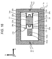
- FIGS. 16 and 17 illustrate modifications of FIGS. 3 and 4
- the acceleration detector 20 is formed of the first laminate 1 similarly to the first embodiment.
- the angular velocity detector 30b is formed with the second laminate 2, while an electrode 39ab forming capacitance with a weight 37b is formed at a position facing the weight 37b, in the first laminate 1.
- the angular velocity detector 30b includes second beams 38ab, 38bb, 38cb, and 38db that join the second weight 37b to the first weight 31, while supporting the second weight 37b with the first weight 31 in a movable state in the direction (z-axis) orthogonal to the paper surface.
- the angular velocity detector 30b includes the second weight 37b movable in the z-direction and also includes an electrode 39ab on the first substrate 1a of the first laminate 1 to form capacitance by facing the second weight 37b in order to detect the displacement amount of the second weight 37b in the z-direction at application of the angular velocity, as a change in capacitance.
- the angular velocity detector 30b includes an electrode 40ab for exchanging signals between the electrode 39ab and an external circuit, and similarly to the above description, the penetrating electrode 50 is connected to the electrode 40ab.
- the angular velocity detector 30b will be described focusing on a difference from the above-described operation of the angular velocity detector 30.
- the angular velocity ⁇ is applied about the y-axis in a state where the first weight 31 and the second weight 37b vibrate in the x-axis direction, and when the mass of the second weight 37b is m 22 , the Coriolis force Fc is generated in the z-axis direction as expressed by the above-described Formula (6). Then, the second weight 37b is displaced by the Coriolis force Fc in the z-axis direction.
- the second weight 37b vibrates in the z-axis direction by the Coriolis force Fc expressed by Formula (6), leading to a change in the capacitance between the second weight 37b and the second electrode 39ab.
- Fc Coriolis force
- the sensor chip 10b can detect acceleration in the y-axis direction and the angular velocity about the y-axis.
- the angular velocity about the x-axis is detected by arranging the angular velocity detector 30 to be rotated by 90 degrees about the z-axis.
- an electrode 39bb may be formed on the second substrate 2b opposite to the weight 37b and the electrode 39ab.
- the insulating portion 27 is provided around a side wall of the electrode 39bb.
- the electrode 25bb is provided on the opposite surface that does not face the weight 21b of the electrode 39bb.
- differential input can be performed to the CV converter 202, making it possible to increase the angular velocity detection sensitivity.
- the acceleration detector 20 may be formed in the second laminate 2, and the electrode 39ab and the electrode 40ab may be formed in the second laminate 2 in the angular velocity detector 30b, with the others formed in the first laminate 1.
- the angular velocity detector 30 may be formed instead of the acceleration detector 20. This enables formation of a sensor chip that detects the angular velocity about two axes, that is, about the z-axis and the y-axis.
- the electrode 39ab and the electrode 40ab may be formed in the second laminate 2, with other electrodes being formed in the first laminate 1 in one angular velocity detector 30b, while the electrode 39ab and the electrode 39ab may be formed in the first laminate 1 with other electrodes being -formed in the second laminate 2 in the other angular velocity detector 30b.
- one of the angular velocity detectors 30b is rotated by 90 degrees about the z-axis with respect to the other angular velocity detector 30b, it is possible to form a sensor chip that detects the angular velocity of each of two axes, that is, the y-axis and the x-axis.
- a sensor chip 10c is constituted with the acceleration detector 20 configured to detect acceleration, the angular velocity detector 30, and a pressure detector 300 that detects pressure.
- FIGS. 19 and 20 detailed descriptions of the same components as those in FIGS. 1 to 18 will be omitted, and different points will be mainly described.
- FIG. 19 illustrates a modification of FIG. 1
- FIG. 20 illustrates a modification of FIG. 2
- the acceleration detector 20 is formed of the first laminate 1 similarly to the first embodiment.
- the angular velocity detector 30 is formed with the second laminate 2.
- the pressure detector 300 is formed with a third laminate 301.
- the pressure detector 300 includes on the substrate 301a a deformable portion 302 that deforms in a direction perpendicular to a plane by applying pressure and includes a cavity 303 formed immediately below the deformable portion 302 in an oxide film 301c, or in the oxide film 301c and a portion of a substrate 301b.
- an electrode 304 is formed on the substrate 301b side opposed to the deformable portion 302 via the cavity 303. At this time, in order to insulate the electrode 304 from the other portion of the second substrate 301b, an insulating portion 305 is provided around a side wall of the electrode 304.
- the deformation of the deformable portion 302 may be configured to detect a change in piezoresistance of the deformable portion 302.
- P 0 and T are the following numerical values.
- the pressure detector 300 in the sensor chip 10c detects the pressure (about 0.1 MPa to 1 MPa) of a gas filled in a tire
- the rotation of the tire or the tire wheel can be detected by the acceleration detector 20 and the angular velocity detector 30, and at the same time, the pressure inside the tire can be detected by the pressure detector 300.
- each of the number of the first laminate. 1, the second laminate 2, and the third laminate may be two.
- the chip packages 4 and 4a may employ a resin substrate or ceramics instead of the lead frame 72 and may be formed as a ball grud array (BGA) package in which electrodes are extracted onto the back surface of the substrate by solder balls.
- BGA ball grud array
Landscapes
- Physics & Mathematics (AREA)
- General Physics & Mathematics (AREA)
- Engineering & Computer Science (AREA)
- Radar, Positioning & Navigation (AREA)
- Remote Sensing (AREA)
- Computer Hardware Design (AREA)
- Microelectronics & Electronic Packaging (AREA)
- Pressure Sensors (AREA)
- Gyroscopes (AREA)
- Micromachines (AREA)
Applications Claiming Priority (2)
| Application Number | Priority Date | Filing Date | Title |
|---|---|---|---|
| JP2015192519 | 2015-09-30 | ||
| PCT/JP2016/072713 WO2017056697A1 (fr) | 2015-09-30 | 2016-08-03 | Capteur d'inertie |
Publications (2)
| Publication Number | Publication Date |
|---|---|
| EP3358357A1 true EP3358357A1 (fr) | 2018-08-08 |
| EP3358357A4 EP3358357A4 (fr) | 2019-11-06 |
Family
ID=58427456
Family Applications (1)
| Application Number | Title | Priority Date | Filing Date |
|---|---|---|---|
| EP16850874.5A Withdrawn EP3358357A4 (fr) | 2015-09-30 | 2016-08-03 | Capteur d'inertie |
Country Status (5)
| Country | Link |
|---|---|
| US (1) | US20180162723A1 (fr) |
| EP (1) | EP3358357A4 (fr) |
| JP (1) | JP6343102B2 (fr) |
| CN (1) | CN108450008A (fr) |
| WO (1) | WO2017056697A1 (fr) |
Families Citing this family (6)
| Publication number | Priority date | Publication date | Assignee | Title |
|---|---|---|---|---|
| JP6420442B1 (ja) * | 2017-10-16 | 2018-11-07 | 株式会社ワコー | 発電素子 |
| US11192664B2 (en) * | 2018-12-10 | 2021-12-07 | Hamilton Sundstrand Corporation | Smart application for aircraft performance data collection |
| AU2021224844A1 (en) * | 2020-02-21 | 2022-10-20 | Nitto Bend Technologies, Inc. | Tire and tire sensor |
| CN215453267U (zh) * | 2021-06-22 | 2022-01-07 | 瑞声声学科技(深圳)有限公司 | 骨传导传感器组件 |
| EP4446281A1 (fr) * | 2023-04-14 | 2024-10-16 | Murata Manufacturing Co., Ltd. | Dispositifs mems à double couche et procédé de fabrication |
| CN116952309B (zh) * | 2023-09-20 | 2023-12-15 | 中国船舶集团有限公司第七〇七研究所 | 一种应用于定向测量设备的姿态和振动监测方法 |
Family Cites Families (13)
| Publication number | Priority date | Publication date | Assignee | Title |
|---|---|---|---|---|
| US5786744A (en) * | 1994-03-24 | 1998-07-28 | Honda Giken Kogyo Kabushiki Kaisha | Hybrid sensor |
| JP3435665B2 (ja) * | 2000-06-23 | 2003-08-11 | 株式会社村田製作所 | 複合センサ素子およびその製造方法 |
| JP2007292499A (ja) * | 2006-04-21 | 2007-11-08 | Sony Corp | モーションセンサ及びその製造方法 |
| DE102006024671A1 (de) * | 2006-05-26 | 2007-11-29 | Robert Bosch Gmbh | Mikromechanisches Bauelement |
| JP4929918B2 (ja) * | 2006-08-21 | 2012-05-09 | パナソニック株式会社 | 複合センサ |
| JP2010217170A (ja) * | 2009-02-17 | 2010-09-30 | Seiko Epson Corp | 複合センサー、電子機器 |
| EP2504711A4 (fr) * | 2009-11-24 | 2014-02-26 | Yost Engineering Inc | Combinaison de capteurs inertiels redondants afin de créer une sortie de capteur virtuelle |
| US8387464B2 (en) * | 2009-11-30 | 2013-03-05 | Freescale Semiconductor, Inc. | Laterally integrated MEMS sensor device with multi-stimulus sensing |
| JP5527015B2 (ja) * | 2010-05-26 | 2014-06-18 | セイコーエプソン株式会社 | 素子構造体、慣性センサー、電子機器 |
| JPWO2012124282A1 (ja) * | 2011-03-11 | 2014-07-17 | パナソニック株式会社 | センサ |
| US9564413B2 (en) * | 2011-09-15 | 2017-02-07 | STATS ChipPAC Pte. Ltd. | Semiconductor device and method of forming semiconductor die with active region responsive to external stimulus |
| JP2013171009A (ja) * | 2012-02-23 | 2013-09-02 | Hitachi Automotive Systems Ltd | 慣性力センサ |
| JP5978170B2 (ja) * | 2013-06-28 | 2016-08-24 | 日立オートモティブシステムズ株式会社 | トランスファーモールド型センサ装置 |
-
2016
- 2016-08-03 WO PCT/JP2016/072713 patent/WO2017056697A1/fr not_active Ceased
- 2016-08-03 US US15/737,389 patent/US20180162723A1/en not_active Abandoned
- 2016-08-03 JP JP2017542980A patent/JP6343102B2/ja not_active Expired - Fee Related
- 2016-08-03 CN CN201680057926.1A patent/CN108450008A/zh active Pending
- 2016-08-03 EP EP16850874.5A patent/EP3358357A4/fr not_active Withdrawn
Also Published As
| Publication number | Publication date |
|---|---|
| US20180162723A1 (en) | 2018-06-14 |
| EP3358357A4 (fr) | 2019-11-06 |
| JP6343102B2 (ja) | 2018-06-13 |
| CN108450008A (zh) | 2018-08-24 |
| WO2017056697A1 (fr) | 2017-04-06 |
| JPWO2017056697A1 (ja) | 2018-03-29 |
Similar Documents
| Publication | Publication Date | Title |
|---|---|---|
| EP3358357A1 (fr) | Capteur d'inertie | |
| US20250155469A1 (en) | Mems tri-axial accelerometer with one or more decoupling elements | |
| US8739626B2 (en) | Micromachined inertial sensor devices | |
| US9247664B2 (en) | Electronic device and manufacturing method thereof, electronic apparatus, and moving body | |
| EP2462408B1 (fr) | Dispositifs capteur inertiel micro-usinés | |
| US8978475B2 (en) | MEMS proof mass with split z-axis portions | |
| US9062972B2 (en) | MEMS multi-axis accelerometer electrode structure | |
| JP5037690B2 (ja) | 微小電気機械システム | |
| EP2284545B1 (fr) | Masses sismiques coplanaires permettant de détecter une accélération le long de trois axes | |
| EP2616772A2 (fr) | Gyroscope à 3 axes monolithiques micro-usinés et à commande unique | |
| JP2013250133A (ja) | 電子デバイス及びその製造方法、並びに電子機器 | |
| JP2012521565A (ja) | 垂直に集積されたmems加速度トランスデューサ | |
| US20230266360A1 (en) | Accelerometer, inertial measurement unit imu, and electronic device | |
| WO2018088065A1 (fr) | Élément de capteur, capteur d'inertie et appareil électronique | |
| JP2010085143A (ja) | 加速度センサー | |
| US11680797B2 (en) | Physical quantity sensor | |
| JP2018132349A (ja) | 物理量検出器および物理量検出装置 | |
| JP5257115B2 (ja) | 力学量センサ及びその製造方法 | |
| Rivers et al. | Micro IMU utilizing folded cube approach | |
| KR20140028991A (ko) | 중첩형 관성 센서 및 그 제어 방법 |
Legal Events
| Date | Code | Title | Description |
|---|---|---|---|
| STAA | Information on the status of an ep patent application or granted ep patent |
Free format text: STATUS: THE INTERNATIONAL PUBLICATION HAS BEEN MADE |
|
| PUAI | Public reference made under article 153(3) epc to a published international application that has entered the european phase |
Free format text: ORIGINAL CODE: 0009012 |
|
| STAA | Information on the status of an ep patent application or granted ep patent |
Free format text: STATUS: REQUEST FOR EXAMINATION WAS MADE |
|
| 17P | Request for examination filed |
Effective date: 20171128 |
|
| AK | Designated contracting states |
Kind code of ref document: A1 Designated state(s): AL AT BE BG CH CY CZ DE DK EE ES FI FR GB GR HR HU IE IS IT LI LT LU LV MC MK MT NL NO PL PT RO RS SE SI SK SM TR |
|
| AX | Request for extension of the european patent |
Extension state: BA ME |
|
| DAV | Request for validation of the european patent (deleted) | ||
| DAX | Request for extension of the european patent (deleted) | ||
| RIC1 | Information provided on ipc code assigned before grant |
Ipc: H01L 29/84 20060101ALI20190517BHEP Ipc: G01P 15/08 20060101ALI20190517BHEP Ipc: G01D 21/02 20060101ALI20190517BHEP Ipc: G01L 9/00 20060101ALI20190517BHEP Ipc: G01P 15/125 20060101ALI20190517BHEP Ipc: G01C 19/5783 20120101AFI20190517BHEP Ipc: G01P 15/18 20130101ALI20190517BHEP Ipc: G01P 1/02 20060101ALI20190517BHEP |
|
| A4 | Supplementary search report drawn up and despatched |
Effective date: 20191004 |
|
| RIC1 | Information provided on ipc code assigned before grant |
Ipc: G01P 15/18 20130101ALI20190927BHEP Ipc: G01C 19/5783 20120101AFI20190927BHEP Ipc: G01D 21/02 20060101ALI20190927BHEP Ipc: G01P 1/02 20060101ALI20190927BHEP Ipc: G01P 15/125 20060101ALI20190927BHEP Ipc: G01P 15/08 20060101ALI20190927BHEP Ipc: H01L 29/84 20060101ALI20190927BHEP Ipc: G01L 9/00 20060101ALI20190927BHEP |
|
| STAA | Information on the status of an ep patent application or granted ep patent |
Free format text: STATUS: THE APPLICATION IS DEEMED TO BE WITHDRAWN |
|
| 18D | Application deemed to be withdrawn |
Effective date: 20200603 |