EP3358496B1 - Vorrichtung und verfahren zur verarbeitung von fingerabdrücken - Google Patents
Vorrichtung und verfahren zur verarbeitung von fingerabdrücken Download PDFInfo
- Publication number
- EP3358496B1 EP3358496B1 EP17154372.1A EP17154372A EP3358496B1 EP 3358496 B1 EP3358496 B1 EP 3358496B1 EP 17154372 A EP17154372 A EP 17154372A EP 3358496 B1 EP3358496 B1 EP 3358496B1
- Authority
- EP
- European Patent Office
- Prior art keywords
- sensor plates
- sensor
- capacitances
- fingerprint
- plates
- Prior art date
- Legal status (The legal status is an assumption and is not a legal conclusion. Google has not performed a legal analysis and makes no representation as to the accuracy of the status listed.)
- Active
Links
Images


Classifications
-
- G—PHYSICS
- G06—COMPUTING OR CALCULATING; COUNTING
- G06V—IMAGE OR VIDEO RECOGNITION OR UNDERSTANDING
- G06V40/00—Recognition of biometric, human-related or animal-related patterns in image or video data
- G06V40/10—Human or animal bodies, e.g. vehicle occupants or pedestrians; Body parts, e.g. hands
- G06V40/12—Fingerprints or palmprints
- G06V40/13—Sensors therefor
- G06V40/1306—Sensors therefor non-optical, e.g. ultrasonic or capacitive sensing
-
- G—PHYSICS
- G01—MEASURING; TESTING
- G01D—MEASURING NOT SPECIALLY ADAPTED FOR A SPECIFIC VARIABLE; ARRANGEMENTS FOR MEASURING TWO OR MORE VARIABLES NOT COVERED IN A SINGLE OTHER SUBCLASS; TARIFF METERING APPARATUS; MEASURING OR TESTING NOT OTHERWISE PROVIDED FOR
- G01D5/00—Mechanical means for transferring the output of a sensing member; Means for converting the output of a sensing member to another variable where the form or nature of the sensing member does not constrain the means for converting; Transducers not specially adapted for a specific variable
- G01D5/12—Mechanical means for transferring the output of a sensing member; Means for converting the output of a sensing member to another variable where the form or nature of the sensing member does not constrain the means for converting; Transducers not specially adapted for a specific variable using electric or magnetic means
- G01D5/14—Mechanical means for transferring the output of a sensing member; Means for converting the output of a sensing member to another variable where the form or nature of the sensing member does not constrain the means for converting; Transducers not specially adapted for a specific variable using electric or magnetic means influencing the magnitude of a current or voltage
- G01D5/24—Mechanical means for transferring the output of a sensing member; Means for converting the output of a sensing member to another variable where the form or nature of the sensing member does not constrain the means for converting; Transducers not specially adapted for a specific variable using electric or magnetic means influencing the magnitude of a current or voltage by varying capacitance
-
- G—PHYSICS
- G06—COMPUTING OR CALCULATING; COUNTING
- G06F—ELECTRIC DIGITAL DATA PROCESSING
- G06F21/00—Security arrangements for protecting computers, components thereof, programs or data against unauthorised activity
- G06F21/30—Authentication, i.e. establishing the identity or authorisation of security principals
- G06F21/31—User authentication
- G06F21/32—User authentication using biometric data, e.g. fingerprints, iris scans or voiceprints
-
- G—PHYSICS
- G06—COMPUTING OR CALCULATING; COUNTING
- G06F—ELECTRIC DIGITAL DATA PROCESSING
- G06F21/00—Security arrangements for protecting computers, components thereof, programs or data against unauthorised activity
- G06F21/30—Authentication, i.e. establishing the identity or authorisation of security principals
- G06F21/31—User authentication
- G06F21/34—User authentication involving the use of external additional devices, e.g. dongles or smart cards
Definitions
- the present disclosure relates to a fingerprint processing system. Furthermore, the present disclosure relates to a corresponding fingerprint processing method and to a corresponding computer program.
- a fingerprint verification device may be used to initiate a payment and to authenticate a user.
- the fingerprint verification device may for example take the form of, or be embedded in, a smart card.
- a smart card may also include a fingerprint sensor for capturing the user's fingerprint. In that case, the captured fingerprint may be used to ascertain that the smart card is presented to a terminal by its rightful owner, for example.
- PIN personal identification number
- Examples of prior art documents implementing sensor reading by selectively activating sensing elements in lines/columns for capacitive fingerprint sensors include US2005/141263 and US2006/158202 . These documents teach how to use orthogonal codes when performing the selective activation of the sensing elements.
- a method of processing a fingerprint in a fingerprint processing system is conceived as defined by the method claim 11.
- a computer program comprising non-transient instructions which, when executed, carry out or control the steps of a method of the kind set forth.
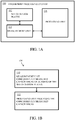
- Fig. 1A shows an illustrative embodiment of a fingerprint processing system 100.
- the fingerprint processing system 100 comprises a set of sensor plates 102 operatively coupled to a measurement unit 104. Furthermore, the fingerprint processing system 100 comprises a processing unit 106 operatively coupled to the measurement unit 104.
- the measurement unit 104 is configured to measure one or more capacitances on the sensor plates 102.
- a measurable capacitance may develop on a sensor plate when a voltage is applied to said plate and an external object, such as a finger, comes into proximity of said plate.
- the sensor plate may act as an electrode and the external object may act as a counter electrode.
- the measurement unit 104 is configured to concurrently measure capacitances on subsets of the set of sensor plates 102.
- the fingerprint processing system 100 comprises a processing unit 106 operatively coupled to the measurement unit 104.
- the processing unit 106 is configured to process measured capacitances, in particular concurrently measured capacitances.
- Fig. 1 B shows an illustrative embodiment of a corresponding fingerprint processing method 108.
- the method 108 comprises, at 110, that the measurement unit 104 concurrently measures capacitances on subsets of the set of sensor plates 102. Furthermore, the method 108 comprises, at 112, that the processing unit 106 processes the capacitances that were concurrently measured by the measurement unit 104. As mentioned above, by concurrently measuring capacitances on subsets of the set of sensor plates 102, the sensitivity of a fingerprint sensor may be increased.
- a fingerprint sensor may need costly manufacturing processes, mainly due to the requirement to expose a coated sensing surface to a cardholder's finger.
- a fingerprint sensor may need a complex module packaging, so as to ensure that the sensor is integrated into a card in such a way that it withstands mechanical stress. Quality requirements of this kind may be prescribed by payment network operators, for example.
- Smart cards often comprise a substrate; the fingerprint sensor may be connected to one side of the substrate, while the finger touches the other side of the substrate. Unfortunately this substrate, which may act as an insulation material, has a certain minimum thickness.
- the presence of insulation material between a cardholder's finger and the active area of a sensor may lead to an attenuation of the measurable effects (e.g., an attenuation of the capacitance change on sensor plates) when a finger comes into proximity of the sensor. This, in turn, may negatively affect the sensitivity of the fingerprint sensor.
- a reduced sensitivity may be corrected by software-implemented techniques (e.g., correlation, filtering and deconvolution), these corrections consume power and require a sufficiently large memory. These correction techniques are therefore less suitable for resource-constrained devices, such as smart cards.
- the presently disclosed system and method may achieve an increased sensitivity without applying the aforementioned correction techniques.
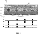
- Fig. 2 shows another illustrative embodiment of a fingerprint processing system 200.
- the fingerprint sensing system 200 comprises a set of sensor plates 202 coupled to a nitride layer 204.
- the nitride layer 204 is coupled to a glue-layer 206.
- the glue-layer 206 is coupled to a substrate 208.
- the fingerprint system 200 may form part of a smart card, for example.
- the substrate 208 may be touched by a finger 212. It is noted that more insulating layers may be present between the finger 212 and the nitride layer 204. Furthermore, a coating may be present between the finger 212 and the substrate 208.
- the term "finger" includes all parts of a finger, such as the finger's papillae.
- the substrate 208 (or the coating, as the case may be) may be touched by the finger's ridges.
- an air gap 210 may exist at locations where the finger 212 does not touch the substrate 208.
- a measurement unit (not shown) may measure the capacitances present on the sensor plates 202 in order to detect the touching of the substrate 208 by the finger 212 at the specific locations of the plates 202. More specifically, when the substrate 208 is touched at a specific location, the capacitance on the sensor plate 202 at that location will change since the finger acts as a counter electrode, and the air gap 210 is absent or small at that location. Thus, the variance in the air gap between the finger's surface and the sensor may indicate the depth of the fingerprint's papillae. By registering and processing the changed capacitances, an image of the fingerprint may be formed.
- a nitride passivation layer 204 having a thickness of e.g. 1.5 ⁇ m that is applied during wafer processing of the sensor
- a glue layer 206 of e.g. 10-25 ⁇ m that may be applied after wafer production by dispensing
- a substrate layer 208 of 50-150 ⁇ m which may be formed by a thermoplastic material such as PET, PVC, polycarbonate or PI.
- more layers may be present between the sensor plates 202 and the surface of the finger 212.
- the average valley depth of a human finger may be assumed to be 20 ⁇ m.
- various dielectric constants may be assigned.
- the indicated thicknesses are corrected by application of the related dielectric constants, so as to yield a distance corresponding to an air gap with similar capacitive properties.
- a dielectric constant of 3 would correct a 150 ⁇ m thick polycarbonate substrate to 50 ⁇ m.
- a layer stack of 2 ⁇ m nitride, 10 um of glue-layer and 150 ⁇ m of substrate yields an additional, virtual air gap of 54 ⁇ m.
- the impact of an additional air gap of 54 ⁇ m is significant. From an electrical perspective the additional air gap reduces the overall capacitance, yielding an attenuated voltage after capacitance-to-voltage conversion. This, in turn, reduces the sensitivity of the sensor.
- capacitances on subsets of the set of sensor plates 202 are measured concurrently, as shown in the lower part of Fig. 2 .
- a first time slot the capacitances C2, C3, and C4 are measured.
- a second time slot the capacitances C1, C3, and C4 are measured.
- a third time slot the capacitances C1, C2, and C4 are measured.
- a fourth time slot the capacitances C1, C2, and C3 are measured.
- capacitances ⁇ C2, C3, C4 ⁇ are measured concurrently
- capacitances ⁇ C1, C3, C4 ⁇ are measured concurrently
- capacitances ⁇ C1, C2, C4 ⁇ are measured concurrently
- capacitances ⁇ C1, C2, C3 ⁇ are measured concurrently.
- the size of a sensor plate determines, among other parameters, the capacitance between said sensor plate and the finger's surface.
- the capacitance of such a sensor plate may e.g. be in the range of 0.5 fF to 20 fF when the finger's surface is in proximity.
- a "virtual sensor plate” By concurrently measuring the capacitances on subsets of the sensor plates, a "virtual sensor plate” is created, which has a larger size than the individual sensor plates 202.
- the higher capacitance measured on this "virtual sensor plate” i.e., higher than the individual capacitances on the sensor plates 202 mitigates the aforementioned attenuation of the measurable effects. This, in turn, increases the sensitivity of the sensor.
- the processing unit is further configured to derive a capacitance on one or more individual sensor plates from the concurrently measured capacitances. For example, the processing unit may perform a calculation that derives the individual capacitances on the sensor plates from the capacitances measured on the subsets. In this way, the fingerprint sensor may be sufficiently sensitive, and at the same time it may still produce a high-resolution fingerprint image. An example of such a calculation is described with reference to Fig. 4 . In a practical and efficient implementation, the subsets are mutually different subsets of the set of sensor plates. Thereby, the calculation of the individual capacitances may be simplified.
- each subset comprises ( n - 1) sensor plates ( n represents the total number of sensor plates in the set), and the measurement unit is configured to sequentially measure the capacitances on n mutually different subsets of the set of sensor plates. This may further facilitate the calculation of the individual capacitances on the sensor plates in the set.
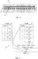
- Fig. 3 shows an illustrative embodiment of an array 300 of sensor plates.
- the array 300 comprises a plurality of sensor plates organized in rows and columns.
- row 302 contains a plurality of sensor plates.
- the capacitances of all but one sensor plate are measured concurrently.
- the capacitance of sensor plate 304 may not be measured, while the capacitances of the other sensor plates in row 302 are measured concurrently.
- sensor plate 304 is not evaluated, while the other sensor plates in row 302 are evaluated concurrently.
- the line scanning sequence shown in Fig. 3 may be applied.
- the image may be scanned line by line (i.e., row by row). In total as many sum evaluations may be applied as the number of sensor plates contained in row 302. In other words, n mutually different subsets of the set of sensor plates may be evaluated sequentially.
- the sensor area is then a multiple of (n - 1) instead of the area of a single sensor plate; thus the output signal is also a multiple compared to signal provided by a single sensor plate.
- Fig. 4 shows an illustrative embodiment of a sampling principle 400 in accordance with the present disclosure.
- the left side of Fig. 4 shows the evaluation 402 of single sensor plates. In other words, the left side of Fig. 4 shows how individual capacitances C1, C2, C3, and C4 are measured sequentially. For example, the individual capacitances may be measured in subsequent cycles or sampling steps.
- the right side of Fig. 4 shows the concurrent evaluation 404 of sensor plates in accordance with the present disclosure. In other words, the right side of Fig. 4 shows how capacitances on subsets of sensor plates are measured concurrently.
- capacitances ⁇ C2, C3, C4 ⁇ are measured concurrently
- capacitances ⁇ C1, C3, C4 ⁇ are measured concurrently
- capacitances ⁇ C1, C2, C4 ⁇ are measured concurrently
- capacitances ⁇ C1, C2, C3 ⁇ are measured concurrently.
- the gain factor is ( n - 1).
- This sampling principle is not limited to a single line or row; it may also be applied to a whole image or to multiple images as long as the fingerprint images do not vary during a sampling period. Furthermore, it is noted that the sampling principle is not limited to sampling exactly n - 1 samples in case of n sensor plates in a line or a row.
- Fig. 5 shows an illustrative embodiment of a switched capacitor integrator 500.
- the measurement unit comprises the switched capacitor integrator 500.
- the switched capacitor integrator 500 facilitates the implementation of the sampling principle illustrated in Fig. 4 .
- the switched capacitor integrator 500 comprises an operational transconductance amplifier (OTA) 502, select switches 504, pre-charge switches 506, a reference voltage source 508, a pre-charge voltage source 510, and a signal-to-data conversion unit 512.
- OTA operational transconductance amplifier
- select switches 504 pre-charge switches 506, a reference voltage source 508, a pre-charge voltage source 510, and a signal-to-data conversion unit 512.
- the creation of the sum samples is realized by the switched capacitor integrator 500.
- the select switches 504 facilitate the selection of sensor plates that should contribute to a sum sample in a given cycle or sampling step.
- Fig. 6 shows an illustrative embodiment of an operation 600 of a switched capacitor integrator.
- the operation 600 comprises the following steps. At 602, all select switches are opened. At 604, the reset switch is closed. At 606, all pre-charge switches are closed. At 610, the reset switch is opened. At 612, dedicated select switches are closed (i.e., the select switches associated with the particular sensor plates in the subset under evaluation). At 614, the OTA output stabilizes during a waiting period. At 616, the OTA output is converted to data. The steps 602 to 616 are repeated for all other sample sums (i.e., for all other subsets that will be evaluated).
- the sequence starts with opening all select switches at 602 and thus preparing to set the initial conditions for all sensor plates.
- the reset switch is closed at 604 to reset the integration capacitor and reset the inverting input node of the OTA to the reference voltage Vref.
- all pre-charge switches are closed at 606, so that all sensor plates are pre-charged to the pre-charge voltage Vpre (which may be 0, for example).
- Vpre which may be 0, for example.
- all pre-charge switches are opened again at 608.
- the reset switch may be opened at 610 to prepare the readout cycle.
- all select switches associated with the sensor plates in the subset under evaluation are closed at 612.
- the OTA provides a current through the integration capacitor CI (shown in Fig. 5 ). This charges all sensor plates in the subset until their voltage is equal to the reference voltage Vref.
- the OTA may provide the charge collected by the integration capacitor CI, which is indicative of the capacitance sum of all sensor plates connected to the inverted OTA input (i.e., the sensor plates in the subset under evaluation.
- a successive signal-to-data converter converts the OTA output into machine readable format at 616.
- Fig. 7 shows an illustrative embodiment of a sensor unit 700.
- the sensor unit 700 comprises a device setup/control and power management block 702, an array control block 704, a sensor array 706, a readout system 708, a data sequencer 710, and a communication interface 716.
- the data sequencer 710 comprises a summer 712 and a gain factor multiplier 714.
- the sensor array 706 comprises a plurality of sensor plates of the kind set forth.
- the readout system 708 may comprise a switched capacitor integrator as shown in Fig. 5 , which operates as shown in Fig. 6 .
- a device setup/control circuit comprised in block 702 may be configured to drive the array control block 704, such that a fingerprint image may be sampled line by line, for example.
- the readout system 708 may provide a series of sum samples that may be summed by a separate summer 712 and that may be multiplied concurrently by the gain factor by the gain factor multiplier 714, in order to simplify consecutive processing. Both the individual sum samples multiplied by the gain factor and the total sum of all sum samples may be communicated through the communication interface 716 to a computing device (not shown) for subsequent calculation of the individual and amplified capacitances.
- the array control block 704 may be may be implemented using configurable shift registers. In that case, predefined loading patterns may control these shift registers, so as to easily realize a desired scanning sequence.
- Fig. 8 shows an illustrative embodiment of data sequencing 800.
- the data sequencing 800 may be carried out by the data sequencer 710 shown in Fig. 7 .
- the data sequencing comprises, at 802, initializing a variable TotalSum with the value 0, and then entering a loop 804 that is executed for each sample sum.
- the loop 804 comprises, at 806, obtaining a sample sum value from the readout system 708, at 808, adding the obtained sample sum value to the variable TotalSum, and, at 810, outputting the sample sum value multiplied by the gain factor.
- the value of variable TotalSum is output to the communication interface 716.
- Fig. 9 shows a further illustrative embodiment of a fingerprint processing system 900.
- the fingerprint processing system 900 comprises a sensor unit 902 that is operatively coupled to a microcontroller unit 904.
- the sensor unit 902 may for example be the same as the sensor unit 700 shown in Fig. 7 .
- the microcontroller unit 904 may embody the presently disclosed processing unit.
- the microcontroller unit 904 may thus process the concurrently measured capacitances on the different subsets of the set of sensor plates present in the sensor unit 902.
- the microcontroller 904 may contain a fingerprint feature extraction unit and a fingerprint template generator (i.e., a generator providing a description of identified minutiae in a list format).
- the microcontroller unit 904 may derive, from the calculated capacitance on an individual sensor plate at a particular location, the distance between a surface of the finger and said sensor plate, and to use said distance for generating a fingerprint image. That is to say, fingerprint features (e.g., minutiae) may be extracted from a plurality of derived distances at different locations in a sensor array. The extracted fingerprint features may be used to create a fingerprint template that can be compared to a stored reference template, with the purpose of authenticating a user, for example.
- fingerprint features e.g., minutiae
- the microcontroller unit 900 may be configured to receive the sum samples and the total sample sum from the sensor unit 902.
- the microcontroller unit 900 may also perform subtractions to derive individual capacitances of specific sensor plates.
- the derived individual capacitance values may be processed by the microprocessor unit 904 in order to derive the corresponding fingerprint valley depths (i.e., the distances between the respective sensor plates and the finger).
- the obtained valley depths may be processed by the feature extraction unit to provide a set of fingerprint features, which may be formatted by the template generator so as to generate a fingerprint template which complies with the input requirements of a subsequent matcher.
- Fig. 10 shows an illustrative embodiment of a fingerprint verification system 1000.
- the system 1000 comprises a biometric template generation unit 1002 (e.g., the fingerprint template generator of the microcontroller 904) operatively coupled to a secure element 1004.
- the secure element 1004 may for example be a chip embedded in a smart card, more specifically a tamper-resistant integrated circuit with installed or pre-installed smartcard-grade applications, for instance payment applications, which have a prescribed functionality and a prescribed level of security.
- the secure element 1004 may implement security functions, such as cryptographic functions and authentication functions.
- the secure element 1004 comprises a payment application, a fingerprint matching component, an operating system and a driver.
- the fingerprint matching component may compare a fingerprint template provided by the biometric template generation 1002 with a stored reference template.
- the system 1000 comprises a payment network 1006 operatively coupled to the secure element 1004, for example through an interface unit (not shown) of a smart card.
- a fingerprint template provided by the biometric template generation unit 1002 may represent the fingerprint of a cardholder.
- the template may be provided through a communication channel to the secure element 1004.
- Said secure element 1004 may be configured to match the received template against a stored reference template that may be linked to the cardholder's identity.
- the fingerprint template generation may be initiated by a payment applet executed under control of an operating system that is implemented on the secure element 1004. In case of a positive match between the received template and the stored reference template, a payment transaction may be authorized. For that purpose the secure element 1004 may be connected to the payment network 1006. If a payment transaction requires authentication, the payment applet executed by the secure element 1004 may request the fingerprint verification.
- the systems and methods described herein may at least partly be embodied by a computer program or a plurality of computer programs, which may exist in a variety of forms both active and inactive in a single computer system or across multiple computer systems.
- they may exist as software program(s) comprised of program instructions in source code, object code, executable code or other formats for performing some of the steps.
- Any of the above may be embodied on a computer-readable medium, which may include storage devices and signals, in compressed or uncompressed form.
- the term “mobile device” refers to any type of portable electronic device, including a cellular telephone, a Personal Digital Assistant (PDA), smartphone, tablet etc.
- the term “computer” refers to any electronic device comprising a processor, such as a general-purpose central processing unit (CPU), a specific-purpose processor or a microcontroller.
- CPU central processing unit
- a computer is capable of receiving data (an input), of performing a sequence of predetermined operations thereupon, and of producing thereby a result in the form of information or signals (an output).
- the term “computer” will mean either a processor in particular or more generally a processor in association with an assemblage of interrelated elements contained within a single case or housing.
- processor or “processing unit” refers to a data processing circuit that may be a microprocessor, a co-processor, a microcontroller, a microcomputer, a central processing unit, a field programmable gate array (FPGA), a programmable logic circuit, and/or any circuit that manipulates signals (analog or digital) based on operational instructions that are stored in a memory.
- memory refers to a storage circuit or multiple storage circuits such as read-only memory, random access memory, volatile memory, non-volatile memory, static memory, dynamic memory, Flash memory, cache memory, and/or any circuit that stores digital information.
- a "computer-readable medium” or “storage medium” may be any means that can contain, store, communicate, propagate, or transport a computer program for use by or in connection with the instruction execution system, apparatus, or device.
- the computer-readable medium may be, for example but not limited to, an electronic, magnetic, optical, electromagnetic, infrared, or semiconductor system, apparatus, device, or propagation medium.
- the computer-readable medium may include the following: an electrical connection having one or more wires, a portable computer diskette, a random access memory (RAM), a read-only memory (ROM), an erasable programmable read-only memory (EPROM or Flash memory), an optical fiber, a portable compact disc read-only memory (CDROM), a digital versatile disc (DVD), a Blu-ray disc (BD), and a memory card.
- RAM random access memory
- ROM read-only memory
- EPROM or Flash memory erasable programmable read-only memory
- CDROM compact disc read-only memory
- DVD digital versatile disc
- BD Blu-ray disc
Landscapes
- Engineering & Computer Science (AREA)
- Physics & Mathematics (AREA)
- General Physics & Mathematics (AREA)
- Human Computer Interaction (AREA)
- Multimedia (AREA)
- Theoretical Computer Science (AREA)
- Image Input (AREA)
- Measurement Of Length, Angles, Or The Like Using Electric Or Magnetic Means (AREA)
Claims (12)
- Fingerabdruck-Verarbeitungssystem, Folgendes umfassend:einen Satz von Sensorplatten,eine Messeinheit, die dafür konfiguriert ist, eine oder mehrere Kapazitäten an den Sensorplatten zu messen,eine Verarbeitungseinheit, die dafür konfiguriert ist, die gemessenen Kapazitäten zu verarbeiten,wobei die Messeinheit dafür konfiguriert ist, gleichzeitig die Kapazitäten von voneinander verschiedenen Teilmengen des Satzes von Sensorplatten zu messen,wobei die Verarbeitungseinheit dafür konfiguriert ist, die gleichzeitig gemessenen Kapazitäten zu verarbeiten,wobei jede Teilmenge (n-1) Sensorplatten umfasst, wobei n die Anzahl der Sensorplatten in dem Satz von Sensorplatten darstellt und wobei die Messeinheit dafür konfiguriert ist, die Kapazitäten von n voneinander verschiedenen Teilmengen des Satzes von Sensorplatten nacheinander zu messen.
- System nach Anspruch 1, wobei die Verarbeitungseinheit ferner dafür konfiguriert ist, eine Kapazität von einer oder mehreren einzelnen Sensorplatten aus den gleichzeitig gemessenen Kapazitäten abzuleiten.
- System nach einem vorhergehenden Anspruch, wobei die Messeinheit einen Switched-Capacitor-Integrator umfasst.
- System nach einem vorhergehenden Anspruch, wobei der Satz von Sensorplatten einer Reihe in einer Anordnung von Sensorplatten entspricht.
- System nach einem der Ansprüche 1 bis 3, wobei der Satz von Sensorplatten mehreren Reihen in einer Anordnung von Sensorplatten entspricht.
- System nach Anspruch 4 oder 5, wobei die Anordnung von Sensorplatten von konfigurierbaren Schieberegistern gesteuert wird.
- System nach einem der Ansprüche 1 bis 3, wobei der Satz von Sensorplatten einem Bild oder mehreren Bildern eines Fingerabdrucks entspricht.
- System nach einem vorhergehenden Anspruch, wobei die Verarbeitungseinheit ein Mikrocontroller ist.
- System nach Anspruch 2, wobei die Verarbeitungseinheit ferner dafür konfiguriert ist, von der Kapazität einer einzelnen Sensorplatte den Abstand zwischen einer Oberfläche des Fingers und der Sensorplatte abzuleiten und den Abstand zum Erzeugen eines Fingerabdruckbildes zu verwenden.
- Fingerabdruck-Bestätigungsvorrichtung, insbesondere eine Smartcard, die das Fingerabdruck-Verarbeitungssystem nach einem vorhergehenden Anspruch umfasst.
- Verfahren zum Verarbeiten eines Fingerabdrucks in einem Fingerabdruck-Verarbeitungssystem, wobei das System einen Satz von Sensorplatten, eine Messeinheit, die dafür konfiguriert ist, eine oder mehrere Kapazitäten an den Sensorplatten zu messen, und eine Verarbeitungseinheit, die dafür konfiguriert ist, die gemessenen Kapazitäten zu verarbeiten, umfasst, wobei das Verfahren Folgendes umfasst:dass die Messeinheit gleichzeitig die Kapazitäten von voneinander verschiedenen Teilmengen des Satzes von Sensorplatten misst,dass die Verarbeitungseinheit die gleichzeitig gemessenen Kapazitäten verarbeitet,wobei jede Teilmenge (n-1) Sensorplatten umfasst, wobei n die Anzahl der Sensorplatten in dem Satz von Sensorplatten darstellt und wobei die Messeinheit die Kapazitäten von n voneinander verschiedenen Teilmengen des Satzes von Sensorplatten nacheinander misst.
- Computerprogramm, nicht-flüchtige Anweisungen umfassend, die bei Ausführung die Schritte des Verfahrens von Anspruch 11 durchführen oder steuern.
Priority Applications (3)
| Application Number | Priority Date | Filing Date | Title |
|---|---|---|---|
| EP17154372.1A EP3358496B1 (de) | 2017-02-02 | 2017-02-02 | Vorrichtung und verfahren zur verarbeitung von fingerabdrücken |
| CN201810100375.3A CN108388843A (zh) | 2017-02-02 | 2018-01-31 | 指纹处理系统和方法 |
| US15/887,953 US10579851B2 (en) | 2017-02-02 | 2018-02-02 | Fingerprint processing system and method |
Applications Claiming Priority (1)
| Application Number | Priority Date | Filing Date | Title |
|---|---|---|---|
| EP17154372.1A EP3358496B1 (de) | 2017-02-02 | 2017-02-02 | Vorrichtung und verfahren zur verarbeitung von fingerabdrücken |
Publications (2)
| Publication Number | Publication Date |
|---|---|
| EP3358496A1 EP3358496A1 (de) | 2018-08-08 |
| EP3358496B1 true EP3358496B1 (de) | 2021-04-07 |
Family
ID=57965744
Family Applications (1)
| Application Number | Title | Priority Date | Filing Date |
|---|---|---|---|
| EP17154372.1A Active EP3358496B1 (de) | 2017-02-02 | 2017-02-02 | Vorrichtung und verfahren zur verarbeitung von fingerabdrücken |
Country Status (3)
| Country | Link |
|---|---|
| US (1) | US10579851B2 (de) |
| EP (1) | EP3358496B1 (de) |
| CN (1) | CN108388843A (de) |
Families Citing this family (6)
| Publication number | Priority date | Publication date | Assignee | Title |
|---|---|---|---|---|
| EP3401835A1 (de) | 2017-05-12 | 2018-11-14 | Nxp B.V. | Fingerabdrucksensormodul |
| EP3511860B1 (de) | 2018-01-11 | 2024-09-11 | Nxp B.V. | Fingerabdrucksensor mit esd-schutz |
| WO2019178272A1 (en) * | 2018-03-13 | 2019-09-19 | Ethernom, Inc. | Secure tamper resistant smart card |
| EP3543897A1 (de) | 2018-03-19 | 2019-09-25 | Nxp B.V. | Fingerabdrucksensor |
| EP3661148B1 (de) | 2018-11-28 | 2023-05-24 | Nxp B.V. | Orts- und identitätsbezogenes authentifizierungsverfahren und kommunikationssystem |
| EP3663779B1 (de) * | 2018-12-05 | 2021-10-06 | Nxp B.V. | Vorrichtung und verfahren zur messung einer kapazität und fingerabdrucksensor mit verwendung davon |
Family Cites Families (19)
| Publication number | Priority date | Publication date | Assignee | Title |
|---|---|---|---|---|
| US6114862A (en) * | 1996-02-14 | 2000-09-05 | Stmicroelectronics, Inc. | Capacitive distance sensor |
| US20030098774A1 (en) * | 2000-03-21 | 2003-05-29 | Chornenky Todd E. | Security apparatus |
| US20020140706A1 (en) | 2001-03-30 | 2002-10-03 | Peterson James R. | Multi-sample method and system for rendering antialiased images |
| JP4036798B2 (ja) * | 2003-07-29 | 2008-01-23 | アルプス電気株式会社 | 容量検出回路および検出方法並びに指紋センサ |
| JP4387773B2 (ja) * | 2003-11-25 | 2009-12-24 | アルプス電気株式会社 | 容量検出回路及び検出方法並びにそれを用いた指紋センサ |
| JP4364609B2 (ja) * | 2003-11-25 | 2009-11-18 | アルプス電気株式会社 | 容量検出回路及びそれを用いた指紋センサ |
| US20120092294A1 (en) * | 2010-10-18 | 2012-04-19 | Qualcomm Mems Technologies, Inc. | Combination touch, handwriting and fingerprint sensor |
| US8564314B2 (en) | 2010-11-02 | 2013-10-22 | Atmel Corporation | Capacitive touch sensor for identifying a fingerprint |
| US9195877B2 (en) * | 2011-12-23 | 2015-11-24 | Synaptics Incorporated | Methods and devices for capacitive image sensing |
| EP2667156B1 (de) | 2012-05-25 | 2015-10-21 | Nxp B.V. | Kapazitives Positionssensorsystem |
| US8767098B2 (en) | 2012-08-30 | 2014-07-01 | Omnivision Technologies, Inc. | Method and apparatus for reducing noise in analog image data of a CMOS image sensor |
| NL2012891B1 (en) | 2013-06-05 | 2016-06-21 | Apple Inc | Biometric sensor chip having distributed sensor and control circuitry. |
| US9152841B1 (en) | 2014-03-24 | 2015-10-06 | Fingerprint Cards Ab | Capacitive fingerprint sensor with improved sensing element |
| TWI557649B (zh) * | 2014-08-01 | 2016-11-11 | 神盾股份有限公司 | 電子裝置及指紋辨識裝置控制方法 |
| US10732771B2 (en) * | 2014-11-12 | 2020-08-04 | Shenzhen GOODIX Technology Co., Ltd. | Fingerprint sensors having in-pixel optical sensors |
| US9449212B2 (en) | 2014-12-22 | 2016-09-20 | Fingerprint Cards Ab | Capacitive fingerprint sensor with sensing elements comprising timing circuitry |
| US9740326B2 (en) * | 2015-03-31 | 2017-08-22 | Synaptics Incorporated | Sensor array with split-drive differential sensing |
| EP3109793B1 (de) * | 2015-06-22 | 2020-07-22 | Nxp B.V. | System zum erkennen von fingerabdrücken |
| EP3401835A1 (de) * | 2017-05-12 | 2018-11-14 | Nxp B.V. | Fingerabdrucksensormodul |
-
2017
- 2017-02-02 EP EP17154372.1A patent/EP3358496B1/de active Active
-
2018
- 2018-01-31 CN CN201810100375.3A patent/CN108388843A/zh not_active Withdrawn
- 2018-02-02 US US15/887,953 patent/US10579851B2/en not_active Expired - Fee Related
Also Published As
| Publication number | Publication date |
|---|---|
| EP3358496A1 (de) | 2018-08-08 |
| CN108388843A (zh) | 2018-08-10 |
| US20180218192A1 (en) | 2018-08-02 |
| US10579851B2 (en) | 2020-03-03 |
Similar Documents
| Publication | Publication Date | Title |
|---|---|---|
| US10579851B2 (en) | Fingerprint processing system and method | |
| US9400880B2 (en) | Method and apparatus for biometric-based security using capacitive profiles | |
| CN106257487B (zh) | 指纹感测系统 | |
| US10509943B2 (en) | Method of processing fingerprint information | |
| KR102170725B1 (ko) | 지문 등록 방법 및 장치 | |
| US9646193B2 (en) | Fingerprint authentication using touch sensor data | |
| Blanco‐Gonzalo et al. | Performance evaluation of handwritten signature recognition in mobile environments | |
| US10552596B2 (en) | Biometric authentication | |
| US9842245B1 (en) | Fingerprint sensing system with liveness detection | |
| CN108363963B (zh) | 指纹验证装置 | |
| US10372966B2 (en) | Fingerprint sensing system and method | |
| Tolosana et al. | Reducing the template ageing effect in on‐line signature biometrics | |
| CN106462758B (zh) | 指纹辨识系统及电子装置 | |
| CN106796652A (zh) | 多视图指纹匹配 | |
| Zareen et al. | Authentic mobile‐biometric signature verification system | |
| TWI694383B (zh) | 具有指紋識別功能的電子裝置及指紋識別方法 | |
| Nguyen et al. | Universal fingerprint minutiae extractor using convolutional neural networks | |
| CN107301549A (zh) | 指纹认证系统和方法 | |
| US20240419770A1 (en) | System and method for secure biometric enrollment | |
| CN110622171A (zh) | 用于拒绝欺骗尝试的指纹认证方法及系统 | |
| US20190286874A1 (en) | Method and electronic device for generating fingerprint information, based on multiple pieces of image information acquired using multiple driving schemes | |
| US10176362B1 (en) | Systems and methods for a gradient-based metric for spoof detection | |
| EP3244342A1 (de) | Biometrische überprüfungsvorrichtung und verfahren | |
| CN107895271A (zh) | 支付方法及装置、计算机装置及计算机可读存储介质 | |
| TWI777282B (zh) | 圖像採集方法、晶片及圖像採集裝置 |
Legal Events
| Date | Code | Title | Description |
|---|---|---|---|
| PUAI | Public reference made under article 153(3) epc to a published international application that has entered the european phase |
Free format text: ORIGINAL CODE: 0009012 |
|
| STAA | Information on the status of an ep patent application or granted ep patent |
Free format text: STATUS: THE APPLICATION HAS BEEN PUBLISHED |
|
| AK | Designated contracting states |
Kind code of ref document: A1 Designated state(s): AL AT BE BG CH CY CZ DE DK EE ES FI FR GB GR HR HU IE IS IT LI LT LU LV MC MK MT NL NO PL PT RO RS SE SI SK SM TR |
|
| AX | Request for extension of the european patent |
Extension state: BA ME |
|
| STAA | Information on the status of an ep patent application or granted ep patent |
Free format text: STATUS: REQUEST FOR EXAMINATION WAS MADE |
|
| 17P | Request for examination filed |
Effective date: 20190208 |
|
| RBV | Designated contracting states (corrected) |
Designated state(s): AL AT BE BG CH CY CZ DE DK EE ES FI FR GB GR HR HU IE IS IT LI LT LU LV MC MK MT NL NO PL PT RO RS SE SI SK SM TR |
|
| GRAP | Despatch of communication of intention to grant a patent |
Free format text: ORIGINAL CODE: EPIDOSNIGR1 |
|
| STAA | Information on the status of an ep patent application or granted ep patent |
Free format text: STATUS: GRANT OF PATENT IS INTENDED |
|
| RIC1 | Information provided on ipc code assigned before grant |
Ipc: G06K 9/00 20060101AFI20200924BHEP |
|
| INTG | Intention to grant announced |
Effective date: 20201013 |
|
| GRAS | Grant fee paid |
Free format text: ORIGINAL CODE: EPIDOSNIGR3 |
|
| GRAA | (expected) grant |
Free format text: ORIGINAL CODE: 0009210 |
|
| STAA | Information on the status of an ep patent application or granted ep patent |
Free format text: STATUS: THE PATENT HAS BEEN GRANTED |
|
| AK | Designated contracting states |
Kind code of ref document: B1 Designated state(s): AL AT BE BG CH CY CZ DE DK EE ES FI FR GB GR HR HU IE IS IT LI LT LU LV MC MK MT NL NO PL PT RO RS SE SI SK SM TR |
|
| REG | Reference to a national code |
Ref country code: GB Ref legal event code: FG4D |
|
| REG | Reference to a national code |
Ref country code: AT Ref legal event code: REF Ref document number: 1380653 Country of ref document: AT Kind code of ref document: T Effective date: 20210415 Ref country code: CH Ref legal event code: EP |
|
| REG | Reference to a national code |
Ref country code: DE Ref legal event code: R096 Ref document number: 602017035995 Country of ref document: DE |
|
| REG | Reference to a national code |
Ref country code: IE Ref legal event code: FG4D |
|
| REG | Reference to a national code |
Ref country code: LT Ref legal event code: MG9D |
|
| REG | Reference to a national code |
Ref country code: NL Ref legal event code: MP Effective date: 20210407 Ref country code: AT Ref legal event code: MK05 Ref document number: 1380653 Country of ref document: AT Kind code of ref document: T Effective date: 20210407 |
|
| PG25 | Lapsed in a contracting state [announced via postgrant information from national office to epo] |
Ref country code: FI Free format text: LAPSE BECAUSE OF FAILURE TO SUBMIT A TRANSLATION OF THE DESCRIPTION OR TO PAY THE FEE WITHIN THE PRESCRIBED TIME-LIMIT Effective date: 20210407 Ref country code: LT Free format text: LAPSE BECAUSE OF FAILURE TO SUBMIT A TRANSLATION OF THE DESCRIPTION OR TO PAY THE FEE WITHIN THE PRESCRIBED TIME-LIMIT Effective date: 20210407 Ref country code: NL Free format text: LAPSE BECAUSE OF FAILURE TO SUBMIT A TRANSLATION OF THE DESCRIPTION OR TO PAY THE FEE WITHIN THE PRESCRIBED TIME-LIMIT Effective date: 20210407 Ref country code: HR Free format text: LAPSE BECAUSE OF FAILURE TO SUBMIT A TRANSLATION OF THE DESCRIPTION OR TO PAY THE FEE WITHIN THE PRESCRIBED TIME-LIMIT Effective date: 20210407 Ref country code: BG Free format text: LAPSE BECAUSE OF FAILURE TO SUBMIT A TRANSLATION OF THE DESCRIPTION OR TO PAY THE FEE WITHIN THE PRESCRIBED TIME-LIMIT Effective date: 20210707 Ref country code: AT Free format text: LAPSE BECAUSE OF FAILURE TO SUBMIT A TRANSLATION OF THE DESCRIPTION OR TO PAY THE FEE WITHIN THE PRESCRIBED TIME-LIMIT Effective date: 20210407 |
|
| REG | Reference to a national code |
Ref country code: DE Ref legal event code: R079 Ref document number: 602017035995 Country of ref document: DE Free format text: PREVIOUS MAIN CLASS: G06K0009000000 Ipc: G06V0010000000 |
|
| PG25 | Lapsed in a contracting state [announced via postgrant information from national office to epo] |
Ref country code: IS Free format text: LAPSE BECAUSE OF FAILURE TO SUBMIT A TRANSLATION OF THE DESCRIPTION OR TO PAY THE FEE WITHIN THE PRESCRIBED TIME-LIMIT Effective date: 20210807 Ref country code: GR Free format text: LAPSE BECAUSE OF FAILURE TO SUBMIT A TRANSLATION OF THE DESCRIPTION OR TO PAY THE FEE WITHIN THE PRESCRIBED TIME-LIMIT Effective date: 20210708 Ref country code: LV Free format text: LAPSE BECAUSE OF FAILURE TO SUBMIT A TRANSLATION OF THE DESCRIPTION OR TO PAY THE FEE WITHIN THE PRESCRIBED TIME-LIMIT Effective date: 20210407 Ref country code: PL Free format text: LAPSE BECAUSE OF FAILURE TO SUBMIT A TRANSLATION OF THE DESCRIPTION OR TO PAY THE FEE WITHIN THE PRESCRIBED TIME-LIMIT Effective date: 20210407 Ref country code: PT Free format text: LAPSE BECAUSE OF FAILURE TO SUBMIT A TRANSLATION OF THE DESCRIPTION OR TO PAY THE FEE WITHIN THE PRESCRIBED TIME-LIMIT Effective date: 20210809 Ref country code: NO Free format text: LAPSE BECAUSE OF FAILURE TO SUBMIT A TRANSLATION OF THE DESCRIPTION OR TO PAY THE FEE WITHIN THE PRESCRIBED TIME-LIMIT Effective date: 20210707 Ref country code: SE Free format text: LAPSE BECAUSE OF FAILURE TO SUBMIT A TRANSLATION OF THE DESCRIPTION OR TO PAY THE FEE WITHIN THE PRESCRIBED TIME-LIMIT Effective date: 20210407 Ref country code: RS Free format text: LAPSE BECAUSE OF FAILURE TO SUBMIT A TRANSLATION OF THE DESCRIPTION OR TO PAY THE FEE WITHIN THE PRESCRIBED TIME-LIMIT Effective date: 20210407 |
|
| REG | Reference to a national code |
Ref country code: DE Ref legal event code: R097 Ref document number: 602017035995 Country of ref document: DE |
|
| PG25 | Lapsed in a contracting state [announced via postgrant information from national office to epo] |
Ref country code: SK Free format text: LAPSE BECAUSE OF FAILURE TO SUBMIT A TRANSLATION OF THE DESCRIPTION OR TO PAY THE FEE WITHIN THE PRESCRIBED TIME-LIMIT Effective date: 20210407 Ref country code: SM Free format text: LAPSE BECAUSE OF FAILURE TO SUBMIT A TRANSLATION OF THE DESCRIPTION OR TO PAY THE FEE WITHIN THE PRESCRIBED TIME-LIMIT Effective date: 20210407 Ref country code: EE Free format text: LAPSE BECAUSE OF FAILURE TO SUBMIT A TRANSLATION OF THE DESCRIPTION OR TO PAY THE FEE WITHIN THE PRESCRIBED TIME-LIMIT Effective date: 20210407 Ref country code: CZ Free format text: LAPSE BECAUSE OF FAILURE TO SUBMIT A TRANSLATION OF THE DESCRIPTION OR TO PAY THE FEE WITHIN THE PRESCRIBED TIME-LIMIT Effective date: 20210407 Ref country code: DK Free format text: LAPSE BECAUSE OF FAILURE TO SUBMIT A TRANSLATION OF THE DESCRIPTION OR TO PAY THE FEE WITHIN THE PRESCRIBED TIME-LIMIT Effective date: 20210407 Ref country code: RO Free format text: LAPSE BECAUSE OF FAILURE TO SUBMIT A TRANSLATION OF THE DESCRIPTION OR TO PAY THE FEE WITHIN THE PRESCRIBED TIME-LIMIT Effective date: 20210407 Ref country code: ES Free format text: LAPSE BECAUSE OF FAILURE TO SUBMIT A TRANSLATION OF THE DESCRIPTION OR TO PAY THE FEE WITHIN THE PRESCRIBED TIME-LIMIT Effective date: 20210407 |
|
| PLBE | No opposition filed within time limit |
Free format text: ORIGINAL CODE: 0009261 |
|
| STAA | Information on the status of an ep patent application or granted ep patent |
Free format text: STATUS: NO OPPOSITION FILED WITHIN TIME LIMIT |
|
| 26N | No opposition filed |
Effective date: 20220110 |
|
| PG25 | Lapsed in a contracting state [announced via postgrant information from national office to epo] |
Ref country code: IS Free format text: LAPSE BECAUSE OF FAILURE TO SUBMIT A TRANSLATION OF THE DESCRIPTION OR TO PAY THE FEE WITHIN THE PRESCRIBED TIME-LIMIT Effective date: 20210807 Ref country code: AL Free format text: LAPSE BECAUSE OF FAILURE TO SUBMIT A TRANSLATION OF THE DESCRIPTION OR TO PAY THE FEE WITHIN THE PRESCRIBED TIME-LIMIT Effective date: 20210407 |
|
| PG25 | Lapsed in a contracting state [announced via postgrant information from national office to epo] |
Ref country code: IT Free format text: LAPSE BECAUSE OF FAILURE TO SUBMIT A TRANSLATION OF THE DESCRIPTION OR TO PAY THE FEE WITHIN THE PRESCRIBED TIME-LIMIT Effective date: 20210407 |
|
| PG25 | Lapsed in a contracting state [announced via postgrant information from national office to epo] |
Ref country code: MC Free format text: LAPSE BECAUSE OF FAILURE TO SUBMIT A TRANSLATION OF THE DESCRIPTION OR TO PAY THE FEE WITHIN THE PRESCRIBED TIME-LIMIT Effective date: 20210407 |
|
| REG | Reference to a national code |
Ref country code: CH Ref legal event code: PL |
|
| REG | Reference to a national code |
Ref country code: BE Ref legal event code: MM Effective date: 20220228 |
|
| PG25 | Lapsed in a contracting state [announced via postgrant information from national office to epo] |
Ref country code: LU Free format text: LAPSE BECAUSE OF NON-PAYMENT OF DUE FEES Effective date: 20220202 |
|
| PG25 | Lapsed in a contracting state [announced via postgrant information from national office to epo] |
Ref country code: LI Free format text: LAPSE BECAUSE OF NON-PAYMENT OF DUE FEES Effective date: 20220228 Ref country code: IE Free format text: LAPSE BECAUSE OF NON-PAYMENT OF DUE FEES Effective date: 20220202 Ref country code: CH Free format text: LAPSE BECAUSE OF NON-PAYMENT OF DUE FEES Effective date: 20220228 |
|
| PG25 | Lapsed in a contracting state [announced via postgrant information from national office to epo] |
Ref country code: BE Free format text: LAPSE BECAUSE OF NON-PAYMENT OF DUE FEES Effective date: 20220228 |
|
| PGFP | Annual fee paid to national office [announced via postgrant information from national office to epo] |
Ref country code: FR Payment date: 20230119 Year of fee payment: 7 |
|
| PGFP | Annual fee paid to national office [announced via postgrant information from national office to epo] |
Ref country code: GB Payment date: 20230121 Year of fee payment: 7 Ref country code: DE Payment date: 20230119 Year of fee payment: 7 |
|
| PG25 | Lapsed in a contracting state [announced via postgrant information from national office to epo] |
Ref country code: HU Free format text: LAPSE BECAUSE OF FAILURE TO SUBMIT A TRANSLATION OF THE DESCRIPTION OR TO PAY THE FEE WITHIN THE PRESCRIBED TIME-LIMIT; INVALID AB INITIO Effective date: 20170202 |
|
| PG25 | Lapsed in a contracting state [announced via postgrant information from national office to epo] |
Ref country code: MK Free format text: LAPSE BECAUSE OF FAILURE TO SUBMIT A TRANSLATION OF THE DESCRIPTION OR TO PAY THE FEE WITHIN THE PRESCRIBED TIME-LIMIT Effective date: 20210407 Ref country code: CY Free format text: LAPSE BECAUSE OF FAILURE TO SUBMIT A TRANSLATION OF THE DESCRIPTION OR TO PAY THE FEE WITHIN THE PRESCRIBED TIME-LIMIT Effective date: 20210407 |
|
| REG | Reference to a national code |
Ref country code: DE Ref legal event code: R119 Ref document number: 602017035995 Country of ref document: DE |
|
| PG25 | Lapsed in a contracting state [announced via postgrant information from national office to epo] |
Ref country code: MT Free format text: LAPSE BECAUSE OF FAILURE TO SUBMIT A TRANSLATION OF THE DESCRIPTION OR TO PAY THE FEE WITHIN THE PRESCRIBED TIME-LIMIT Effective date: 20210407 |
|
| GBPC | Gb: european patent ceased through non-payment of renewal fee |
Effective date: 20240202 |
|
| PG25 | Lapsed in a contracting state [announced via postgrant information from national office to epo] |
Ref country code: DE Free format text: LAPSE BECAUSE OF NON-PAYMENT OF DUE FEES Effective date: 20240903 |
|
| PG25 | Lapsed in a contracting state [announced via postgrant information from national office to epo] |
Ref country code: GB Free format text: LAPSE BECAUSE OF NON-PAYMENT OF DUE FEES Effective date: 20240202 |
|
| PG25 | Lapsed in a contracting state [announced via postgrant information from national office to epo] |
Ref country code: FR Free format text: LAPSE BECAUSE OF NON-PAYMENT OF DUE FEES Effective date: 20240229 |
|
| PG25 | Lapsed in a contracting state [announced via postgrant information from national office to epo] |
Ref country code: GB Free format text: LAPSE BECAUSE OF NON-PAYMENT OF DUE FEES Effective date: 20240202 Ref country code: FR Free format text: LAPSE BECAUSE OF NON-PAYMENT OF DUE FEES Effective date: 20240229 Ref country code: DE Free format text: LAPSE BECAUSE OF NON-PAYMENT OF DUE FEES Effective date: 20240903 |
|
| PG25 | Lapsed in a contracting state [announced via postgrant information from national office to epo] |
Ref country code: TR Free format text: LAPSE BECAUSE OF FAILURE TO SUBMIT A TRANSLATION OF THE DESCRIPTION OR TO PAY THE FEE WITHIN THE PRESCRIBED TIME-LIMIT Effective date: 20210407 |