EP3358630A1 - Panneaux photovoltaïques partiellement translucides et leurs procédés de fabrication - Google Patents
Panneaux photovoltaïques partiellement translucides et leurs procédés de fabrication Download PDFInfo
- Publication number
- EP3358630A1 EP3358630A1 EP17154742.5A EP17154742A EP3358630A1 EP 3358630 A1 EP3358630 A1 EP 3358630A1 EP 17154742 A EP17154742 A EP 17154742A EP 3358630 A1 EP3358630 A1 EP 3358630A1
- Authority
- EP
- European Patent Office
- Prior art keywords
- thin film
- film photovoltaic
- electrically conductive
- busbar
- photovoltaic
- Prior art date
- Legal status (The legal status is an assumption and is not a legal conclusion. Google has not performed a legal analysis and makes no representation as to the accuracy of the status listed.)
- Granted
Links
Images




Classifications
-
- H—ELECTRICITY
- H10—SEMICONDUCTOR DEVICES; ELECTRIC SOLID-STATE DEVICES NOT OTHERWISE PROVIDED FOR
- H10F—INORGANIC SEMICONDUCTOR DEVICES SENSITIVE TO INFRARED RADIATION, LIGHT, ELECTROMAGNETIC RADIATION OF SHORTER WAVELENGTH OR CORPUSCULAR RADIATION
- H10F19/00—Integrated devices, or assemblies of multiple devices, comprising at least one photovoltaic cell covered by group H10F10/00, e.g. photovoltaic modules
- H10F19/30—Integrated devices, or assemblies of multiple devices, comprising at least one photovoltaic cell covered by group H10F10/00, e.g. photovoltaic modules comprising thin-film photovoltaic cells
-
- H—ELECTRICITY
- H10—SEMICONDUCTOR DEVICES; ELECTRIC SOLID-STATE DEVICES NOT OTHERWISE PROVIDED FOR
- H10F—INORGANIC SEMICONDUCTOR DEVICES SENSITIVE TO INFRARED RADIATION, LIGHT, ELECTROMAGNETIC RADIATION OF SHORTER WAVELENGTH OR CORPUSCULAR RADIATION
- H10F19/00—Integrated devices, or assemblies of multiple devices, comprising at least one photovoltaic cell covered by group H10F10/00, e.g. photovoltaic modules
- H10F19/90—Structures for connecting between photovoltaic cells, e.g. interconnections or insulating spacers
-
- H—ELECTRICITY
- H10—SEMICONDUCTOR DEVICES; ELECTRIC SOLID-STATE DEVICES NOT OTHERWISE PROVIDED FOR
- H10F—INORGANIC SEMICONDUCTOR DEVICES SENSITIVE TO INFRARED RADIATION, LIGHT, ELECTROMAGNETIC RADIATION OF SHORTER WAVELENGTH OR CORPUSCULAR RADIATION
- H10F19/00—Integrated devices, or assemblies of multiple devices, comprising at least one photovoltaic cell covered by group H10F10/00, e.g. photovoltaic modules
- H10F19/30—Integrated devices, or assemblies of multiple devices, comprising at least one photovoltaic cell covered by group H10F10/00, e.g. photovoltaic modules comprising thin-film photovoltaic cells
- H10F19/31—Integrated devices, or assemblies of multiple devices, comprising at least one photovoltaic cell covered by group H10F10/00, e.g. photovoltaic modules comprising thin-film photovoltaic cells having multiple laterally adjacent thin-film photovoltaic cells deposited on the same substrate
- H10F19/37—Integrated devices, or assemblies of multiple devices, comprising at least one photovoltaic cell covered by group H10F10/00, e.g. photovoltaic modules comprising thin-film photovoltaic cells having multiple laterally adjacent thin-film photovoltaic cells deposited on the same substrate comprising means for obtaining partial light transmission through the integrated devices, or the assemblies of multiple devices, e.g. partially transparent thin-film photovoltaic modules for windows
-
- H—ELECTRICITY
- H10—SEMICONDUCTOR DEVICES; ELECTRIC SOLID-STATE DEVICES NOT OTHERWISE PROVIDED FOR
- H10F—INORGANIC SEMICONDUCTOR DEVICES SENSITIVE TO INFRARED RADIATION, LIGHT, ELECTROMAGNETIC RADIATION OF SHORTER WAVELENGTH OR CORPUSCULAR RADIATION
- H10F19/00—Integrated devices, or assemblies of multiple devices, comprising at least one photovoltaic cell covered by group H10F10/00, e.g. photovoltaic modules
- H10F19/90—Structures for connecting between photovoltaic cells, e.g. interconnections or insulating spacers
- H10F19/902—Structures for connecting between photovoltaic cells, e.g. interconnections or insulating spacers for series or parallel connection of photovoltaic cells
-
- H—ELECTRICITY
- H10—SEMICONDUCTOR DEVICES; ELECTRIC SOLID-STATE DEVICES NOT OTHERWISE PROVIDED FOR
- H10F—INORGANIC SEMICONDUCTOR DEVICES SENSITIVE TO INFRARED RADIATION, LIGHT, ELECTROMAGNETIC RADIATION OF SHORTER WAVELENGTH OR CORPUSCULAR RADIATION
- H10F71/00—Manufacture or treatment of devices covered by this subclass
-
- Y—GENERAL TAGGING OF NEW TECHNOLOGICAL DEVELOPMENTS; GENERAL TAGGING OF CROSS-SECTIONAL TECHNOLOGIES SPANNING OVER SEVERAL SECTIONS OF THE IPC; TECHNICAL SUBJECTS COVERED BY FORMER USPC CROSS-REFERENCE ART COLLECTIONS [XRACs] AND DIGESTS
- Y02—TECHNOLOGIES OR APPLICATIONS FOR MITIGATION OR ADAPTATION AGAINST CLIMATE CHANGE
- Y02E—REDUCTION OF GREENHOUSE GAS [GHG] EMISSIONS, RELATED TO ENERGY GENERATION, TRANSMISSION OR DISTRIBUTION
- Y02E10/00—Energy generation through renewable energy sources
- Y02E10/50—Photovoltaic [PV] energy
Definitions
- the present disclosure relates to methods for fabricating photovoltaic modules of a predetermined size and shape, and more in particular to methods for fabricating partially translucent, e.g. partially transparent, thin film photovoltaic modules of a predetermined size and shape.
- the present disclosure further relates to photovoltaic modules, more in particular to partially translucent, e.g. partially transparent, thin film photovoltaic modules of a predetermined size and shape.
- Partially transparent thin film photovoltaic modules are known. They are only available in relatively small sizes, such as for example with a width of 150 cm and a length of 60 cm. Size limitations of thin film photovoltaic modules may for example be related to size limitations of the equipment used for fabricating thin film photovoltaic modules. However, for building integrated photovoltaic applications, wherein for example window elements or facade elements having typical dimensions in the range between 2 to 4 m by 1 to 2 m are used, the available sizes may not be suitable. For building integrated photovoltaic applications there is also a need to provide different photovoltaic module sizes, for example any photovoltaic module size, e.g. non-standard size, for example to comply with architects' requirements.
- the thin film photovoltaic modules may for example comprise photovoltaic cells based on chalcogenide materials such as e.g. CdTe (Cadmium Telluride), CIS (Copper Indium Selenide), CGS (Copper Gallium Selenide), CIGS (Copper Indium Gallium Selenide, Copper Indium Gallium Sulfide), e.g. kesterites such as CZTS (Copper Zinc Tin Sulfide, Copper Zinc Tin Selenide), amorphous silicon, microcrystalline silicon, polycrystralline silicon, organic materials or perovskite materials, the present disclosure not being limited thereto.
- methods described herein may also be applied to other than thin film photovoltaic modules, e.g. wafer based photovoltaic modules, such as for example polycrystalline or monocrystalline silicon photovoltaic modules.
- the present disclosure is related to a method for electrically interconnecting a plurality of thin film photovoltaic plates, wherein the method comprises: positioning a plurality of thin film photovoltaic plates next to each other side by side, each of the plurality of thin film photovoltaic plates comprising a first plate electrode of a first polarity and a second plate electrode of a second polarity opposite to the first polarity; providing a connection element comprising a plurality of electrically conductive wires arranged in a grid structure on a surface of each of the plurality of thin film photovoltaic plates; dividing each connection element in a first connection part comprising a plurality of first electrically conductive wires and a second connection part comprising a plurality of second electrically conductive wires, thereby separating and electrically insulating the plurality of first electrically conductive wires from the plurality of second electrically conductive wires; forming, for each of the plurality of thin film photovoltaic plates, a first electrical connection
- the surface on which the connection element is provided may be a front surface of the photovoltaic plates.
- the present disclosure is not limited thereto.
- the surface on which the connection element is provided may be the back surface of the photovoltaic plates.
- part of the plurality of thin film photovoltaic plates e.g.
- the surface on which the connection element is provided may be the front surface and for the remaining part of the plurality of thin film photovoltaic plates the surface on which the connection element is provided may be the back surface of the photovoltaic plates.
- each of the plurality of thin film photovoltaic plates may comprise a plurality of thin film photovoltaic cells, each cell comprising a first cell electrode and a second cell electrode.
- the method in accordance with the present disclosure may further comprise providing an optically transparent electrically insulating layer on the surface of the plurality of thin film photovoltaic plates on which the connection element is provided, to thereby electrically insulate the first cell electrodes and the second cell electrodes from the connection element.
- the optically transparent electrically insulating layer may be provided before providing the connection elements.
- the optically transparent electrically insulating layer and the connection element may be provided simultaneously.
- the connection element may be integrated with, e.g. attached to, the optically transparent electrically insulating layer before they are provided on the surface of a photovoltaic plate.
- forming the first electrical connection and forming the second electrical connection may for example comprise welding, soldering, gluing, pressing, printing of an electrically conductive structure, welding of an electrically conductive structure or soldering of an electrically conductive structure or any combination thereof.
- forming the first busbar connection and forming the second busbar connection may comprise welding, soldering, gluing, pressing, printing of an electrically conductive structure, welding of an electrically conductive structure or soldering of an electrically conductive structure or any combination thereof.
- forming the first busbar connections and forming the second busbar connections results in the plurality of photovoltaic plates being electrically interconnected with each other.
- the plurality of photovoltaic plates within a photovoltaic module is electrically interconnected in parallel.
- the present disclosure is not limited thereto.
- the plurality of photovoltaic plates may be electrically interconnected in series, or a combination of parallel and series interconnections may be used.
- connection element may for example have an optical transparency of more than 90%, preferably more than 95%, preferably more than 98%, the present disclosure not being limited thereto.
- connection element may for example have a sheet resistance lower than 10 Ohm per square, preferably lower than 2 Ohm per square, preferably lower than 0.5 Ohm per square, preferably lower than 0.1 Ohm per square, the present disclosure not being limited thereto.
- the present disclosure is related to a method for manufacturing a thin film photovoltaic module, wherein the method comprises: providing a plurality of thin film photovoltaic plates comprising a first plate electrode of a first polarity and a second plate electrode of a second polarity opposite to the first polarity; providing a first encapsulation sheet; electrically interconnecting the plurality of thin film photovoltaic plates by a method according to an embodiment of the first aspect, wherein providing the first busbar of the first polarity and the second busbar of the second polarity comprises providing the first busbar and the second busbar on the first encapsulation sheet and wherein positioning the plurality of thin film photovoltaic plates next to each other side by side comprises positioning the plurality of thin film photovoltaic plates on the first encapsulation sheet having the first busbar and the second busbar provided thereon, thereby leaving the first busbar and the second busbar at least partially exposed.
- the first encapsulation sheet may correspond to a front encapsulation sheet (front plate, cover sheet, cover plate) or to a back encapsulation sheet (back plate, carrier sheet, carrier plate) of the photovoltaic module.
- a method according to the second aspect of the present disclosure further comprises providing a second encapsulation sheet on the plurality of thin film photovoltaic plates (at a side of the thin film photovoltaic plates opposite to the side of the first encapsulation sheet) and performing a lamination step to thereby encapsulate the plurality of thin film photovoltaic plates in between the first encapsulation sheet and the second encapsulation sheet and to thereby form a thin film photovoltaic module.
- the second encapsulation sheet corresponds to a back or rear encapsulation sheet of the photovoltaic module, and vice versa
- the first plate corresponds to a back encapsulation sheet
- the second plate corresponds to a front encapsulation sheet
- a method according to the second aspect of the present disclosure may further comprise providing an encapsulation layer, the encapsulation layer being provided in between the plurality of thin film photovoltaic plates and at least one of the first encapsulation sheet and the second encapsulation sheet.
- the connection element may be provided separately or it may for example be integrated with the encapsulation layer.
- the optically transparent electrically insulating layer, the connection element and the encapsulation layer may be integrated into a single sheet, before they are provided on a surface of the plurality of thin film photovoltaic plates.
- the connection element may be integrated with, e.g. provided on a surface of, the second encapsulation sheet.
- the plurality of photovoltaic plates within a photovoltaic module is electrically interconnected in parallel.
- the present disclosure is not limited thereto.
- the plurality of photovoltaic plates may be electrically interconnected in series, or a combination of parallel and series interconnections may be used.
- placing the plurality of thin film photovoltaic plates next to each other side by side may comprise positioning the plurality of plates with a plate electrode of a same polarity facing each other.
- the plurality of thin film photovoltaic plates may be positioned such that the first plate electrode of a thin film photovoltaic plate is positioned next to the first plate electrode of a neighboring thin film photovoltaic plate.
- the plurality of thin film photovoltaic plates may be positioned such that the second plate electrode of a thin film photovoltaic plate is positioned next to the second plate electrode of a neighboring photovoltaic plate. It is an advantage of such embodiments that a relatively easy parallel electrical interconnection may be established between the photovoltaic plates.
- the present disclosure is not limited thereto and other relative photovoltaic plate positions or orientations may be used.
- positioning the plurality of thin film photovoltaic plates may comprise arranging the plurality of thin film photovoltaic plates in a linear array. In embodiments of the present disclosure, positioning the plurality of thin film photovoltaic plates may comprise arranging the plurality of thin film photovoltaic plates in a two-dimensional array.
- the present disclosure is related to a thin film photovoltaic module comprising: a plurality of thin film photovoltaic plates positioned next to each other side by side, each of the thin film photovoltaic plates comprising a first plate electrode of a first polarity and a second plate electrode of a second polarity opposite to the first polarity; for each of the plurality of thin film photovoltaic plates, a connection element provided on a surface of the plurality of thin film photovoltaic plates, the connection element comprising a plurality of electrically conductive wires arranged in a grid structure and divided in a first connection part comprising a plurality of first electrically conductive wires and a second connection part comprising a plurality of second electrically conductive wires, the plurality of first electrically conductive wires being electrically insulated from the plurality of second electrically conductive wires; for each of the plurality of thin film photovoltaic plates, a first electrical connection between corresponding first electrically conductive wires and the first
- relatively large thin film photovoltaic modules of any size may be provided, such as for example a size up to 4 m by 2 m, the present disclosure not being limited thereto. It is an advantage of methods and devices in accordance with embodiments of the present disclosure that such relatively large thin film photovoltaic modules may be partially translucent, e.g. partially transparent, the present disclosure not being limited thereto.
- thin film photovoltaic modules of different sizes may be provided wherein the modules have a same output, such as for example a same output voltage, independent of their size.
- a plurality of thin film photovoltaic plates having a same output voltage may be electrically interconnected in parallel to form a module of any desired size, such that an output voltage of the module is independent on the number of interconnected thin film photovoltaic plates and thus independent on the module size.
- a same or similar electrical interconnection technology may be used for non-translucent and partially translucent, e.g. partially transparent, photovoltaic modules.
- a same or a similar electrical interconnection technology may be used for thin film photovoltaic modules and for wafer based photovoltaic modules.
- photovoltaic plates having a standard, commercially available, size may be used for forming photovoltaic modules of any desired size. It is an advantage that this allows using the available mass production equipment for fabricating the plates, leading to a cost-effective solution.
- the module encapsulation may done simultaneously with the formation of electrical connections to the plurality of photovoltaic plates, the formation of electrical interconnections between the plurality of photovoltaic plates, and/or with the step of providing an insulating material between the plurality of photovoltaic plates and the connection element. Therefore, the number of manufacturing steps may be reduced, which may result in a reduction of manufacturing costs.
- connection element is integrated with or attached to a carrier, such as for example an encapsulation layer or for example an encapsulation sheet, that it may ease processing and handling of the connection element and/or it may improve its dimensional stability and structural integrity.
- a carrier such as for example an encapsulation layer or for example an encapsulation sheet
- Photovoltaic modules according to embodiments of the third aspect of the present disclosure may advantageously be used for building integrated applications.
- photovoltaic modules according to embodiments of the third aspect of the present disclosure that the presence within the module of connection elements comprising a plurality of electrically conductive wires may mechanically reinforce the photovoltaic modules, e.g. in a similar way as in wire reinforced glass.
- photovoltaic modules Although in the description provided herein the focus is on thin film photovoltaic modules, the present disclosure is not limited thereto and the same or similar methods may also be used for other types of photovoltaic modules, such as for example wafer based photovoltaic modules, e.g. crystalline silicon photovoltaic modules.
- a thin film is a thin layer or thin coating having a thickness in the range between 10 nm and 10 micrometers.
- a thin film photovoltaic cell is a photovoltaic cell wherein the different layers forming the cell are thin layers, typically made by deposition of a stack of thin layers on a substrate such as a glass substrate, a plastic substrate or a metal substrate, the present disclosure not being limited thereto.
- This definition of a thin film photovoltaic cell does not exclude the presence of even thinner layers within the thin film photovoltaic cell structure, such as for example thin passivation layers or tunnel layers, e.g. having a thickness that may be less than 10 nm.
- a thin film photovoltaic stack is a stack comprising thin layers forming a thin film photovoltaic cell, wherein the stack comprises at least an active layer or active layer stack for light absorption and charge carrier separation, a first contact layer of a first polarity and a second contact layer of a second polarity opposite to the first polarity.
- the active layer stack may for example comprise an n-type semiconductor layer and a p-type semiconductor layer.
- additional layers may be included, such as for example an intrinsic semiconductor layer, a hole transporting layer, a hole blocking layer, an electron transporting layer and/or an electron blocking layer, the present disclosure not being limited thereto.
- a thin film photovoltaic plate is a structure comprising a substrate, such as for example a glass substrate, a plastic substrate or a metal substrate, with a thin film photovoltaic stack deposited thereon.
- the thin film photovoltaic stack may be patterned to form a plurality of photovoltaic cells monolithically integrated on the substrate and electrically interconnected for example in series, the present disclosure not being limited thereto.
- a photovoltaic plate does not contain external electrical connections. It is not encapsulated, such that the photovoltaic stack is exposed at a side opposite to the substrate side, i.e. not covered by another layer such as an encapsulation layer or an encapsulation sheet (encapsulation plate).
- a photovoltaic module is a photovoltaic device comprising a plurality of electrically interconnected photovoltaic cells embedded between a back encapsulation sheet, e.g. rear carrier or rear substrate, and a front encapsulation sheet, e.g. front carrier, front cover or superstrate, and further comprising a module frame and external electrical connections, for example for further electrical connection to another photovoltaic module or to a load.
- a photovoltaic module may further comprise additional elements, such as for example a junction box, a maximum power point tracker and appropriate wiring and electrical connections. These additional elements may for example be integrated within the module frame.
- the plurality of electrically interconnected photovoltaic cells may be monolithically integrated on one or more substrates (such as for example in case of thin film photovoltaic cells / modules) or they may be provided each with their own substrate (such as for example in case of wafer based cells / modules).
- the front surface or front side of a photovoltaic cell, of a photovoltaic plate or of a photovoltaic module is the surface or side adapted for being oriented towards a light source and thus for receiving illumination.
- both surfaces are adapted to receive impinging light.
- the front surface or front side is the surface or side adapted for receiving the largest fraction of the light or illumination.
- the back surface, rear surface, back side or rear side of a photovoltaic cell, a photovoltaic plate or a photovoltaic module is the surface or side opposite to the front surface or side.
- connection elements comprising a plurality of electrically conductive wires.
- the term 'wires' also includes ribbons, such as for example threads, rods, lines or strips, the present disclosure not being limited thereto.
- Wires or ribbons as used herein may for example be provided in the form of a fabric, e.g. a woven fabric, or they may for example be printed or plated on a substrate, such as on a foil, e.g. an insulating foil, the present disclosure not being limited thereto.
- 'wires' may for example also refer to elements of expanded metal mesh structures, the present disclosure not being limited thereto.
- translucency includes transparency, i.e. transparency is a subset of translucency.
- Transparency refers to the physical property of allowing light to pass through without being scattered.
- Translucency refers to the physical property of allowing light to pass through, wherein the photons may be scattered or not.
- 'translucent' or 'translucency' when 'translucent' or 'translucency' is used it is understood that this also includes 'transparent' or 'transparency'.
- the present disclosure relates to methods for electrically interconnecting a plurality of thin film photovoltaic plates positioned next to each other side by side, each of the thin film photovoltaic plates comprising a first plate electrode of a first polarity and a second plate electrode of a second polarity opposite to the first polarity.
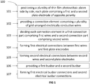
- FIG 1 An example of process steps of a method according to an embodiment of the first aspect of the present disclosure is schematically illustrated in FIG 1 .
- the method 100 illustrated in FIG 1 comprises positioning ( FIG 1 , step 101) a plurality of thin film photovoltaic plates next to each other side by side.
- each of the thin film photovoltaic plates comprises a first plate electrode of a first polarity and a second plate electrode of a second polarity opposite to the first polarity.
- the first plate electrode and the second plate electrode are exposed at least partially, i.e. the first plate electrode and the second plate electrode are not fully covered by another layer. This allows providing an electrical connection to the first plate electrode and the second plate electrode in a further process step of a method 100.
- the plurality of thin film photovoltaic plates may be positioned next to each other such that for neighboring photovoltaic plates the electrodes of a same polarity are located next to each other.
- the plurality of thin film photovoltaic plates may be placed next to each other with their first plate electrode next to the first plate electrode of a neighboring photovoltaic plate and/or with their second plate electrode next to the second plate electrode of a neighboring photovoltaic plate, thus facilitating a relatively easy parallel electrical interconnection of the thin film photovoltaic plates in a later process step.
- FIG 3 schematically illustrates an example of a cross section of a (part of) a thin film photovoltaic plate 10, as may for example be used in embodiments of the present disclosure.
- the thin film photovoltaic plate shown in FIG 3 comprises a substrate 11 on which a plurality of patterned layers is provided, more in particular a first patterned layer forming a plurality of first cell electrodes 13, a second patterned layer forming a plurality of cell active layers 12 and a third patterned layer forming a plurality of second cell electrodes 14, the plurality of second cell electrodes 14 having a polarity opposite to a polarity of the plurality of first cell electrodes 13.
- Each stack comprising a first cell electrode 13, a cell active layer 12 and a second cell electrode 14 forms a thin film photovoltaic cell 15.
- the substrate 11 may for example be a glass substrate, a plastic substrate such as a plastic foil, a semiconductor substrate, a composite substrate or a metal foil such as a steel foil, the present disclosure not being limited thereto.
- the substrate is a translucent, e.g. transparent, substrate such as a glass substrate or a translucent, e.g. transparent, plastic substrate.
- the patterned layers 12, 13, 14 form a plurality of thin film photovoltaic cells 15 that are electrically interconnected in series.
- the plurality of first cell electrodes 13 is provided on the substrate 11 and may comprise any suitable electrically conductive material, for example a metal, such as copper, gold, silver, molybdenum or platinum, a metal alloy, an electrically conductive oxide or an electrically conductive polymer.
- the active layer 12 is patterned to form the plurality of photovoltaic cells 15. It may comprise more than one thin film layer, for example a plurality of stacked layers, i.e. the active layer 12 may be a stack comprising a plurality of thin film layers.
- the absorber layer may for example be a layer comprising a chalcogenide semiconductor material such as e.g. CdTe (Cadmium Telluride), CIS (Copper Indium Selenide), CGS (Copper Gallium Selenide), CIGS (Copper Indium Gallium Selenide, Copper Indium Gallium Sulfide), e.g.
- the active layer 12 may further comprise a second thin film semiconductor layer forming a homo-junction or a hetero-junction with the first thin film semiconductor layer, enabling separation of light-generated charge carriers.
- the active layer may comprise a single junction or it may comprise more than one junction (tandem cell).
- the active layer 12 may further comprise a charge transport layer (a hole transport layer and/or an electron transport layer), for example for facilitating charge transport towards the first cell electrode 13 and/or towards the second cell electrode 14.
- the active layer 12 may further comprise a charge injection layer (a hole injection layer and/or an electron injection layer), for example for reducing a contact resistance between the active layer 12 and the first cell electrode 13 and/or for reducing a contact resistance between the active layer 12 and the second cell electrode 14.
- the plurality of second cell electrodes 14 may comprise any suitable electrically conductive material, for example a metal, such as copper, gold, silver, molybdenum or platinum, a metal alloy, an electrically conductive oxide or an electrically conductive polymer.
- At least one of the plurality of first cell electrodes 13 and the plurality of second cell electrodes is made of a substantially transparent electrically conductive material, such as for example a TCO (Transparent Conductive Oxide), such as for example Indium Tin Oxide or Zinc Oxide, or graphene, the present disclosure not being limited thereto.
- a substantially transparent electrically conductive material such as for example a TCO (Transparent Conductive Oxide), such as for example Indium Tin Oxide or Zinc Oxide, or graphene, the present disclosure not being limited thereto.
- at least the plurality of cell electrodes located closest to a front side (i.e. light receiving side) of the photovoltaic plates is made of a substantially transparent electrically conductive material.
- the front side of a photovoltaic plate 10 may correspond to the substrate side or it may correspond to the side opposite to the substrate side.
- each second cell electrode 14 is electrically connected to the first cell electrode 13 of a neighboring photovoltaic cell, such that all photovoltaic cells 15 provided on the substrate 11 are electrically interconnected in series.
- the present disclosure is not limited thereto.
- an initial, as-fabricated thin film photovoltaic plate 9 may be cut into two or more smaller photovoltaic plates 10, so as to obtain photovoltaic plates of a predetermined, smaller size. This is schematically illustrated in FIG 4(a) , showing a top view of an initial photovoltaic plate 9 having a length L plate and an initial width W plate, initial .
- initial, as-fabricated thin film photovoltaic plates 9 may be used instead of cutting them into smaller photovoltaic plates 10.
- FIG 4(a) schematically shows a cutting line 1, as an example of a line along which the initial photovoltaic plate 9 maybe cut to obtain two photovoltaic plates 10 of smaller size.
- the cutting line 1 is oriented substantially orthogonal to a longitudinal direction (width direction) of the rectangular shaped photovoltaic cells.
- the present disclosure is not limited thereto.
- FIG 4(b) schematically shows a top view of a cut photovoltaic plate 10, in the example shown having the same length L plate as the initial photovoltaic plate and having a smaller width W plate,cut .
- the smaller, cut photovoltaic plates 10 may be used for forming thin film photovoltaic modules of a predetermined size and shape.
- the present disclosure is not limited thereto, and in embodiments of the present disclosure also initial, as-fabricated thin film photovoltaic plates 9 maybe used instead of smaller photovoltaic plates 10 for forming thin film photovoltaic modules of a predetermined size and shape.
- Typical initial dimensions of commercially fabricated thin film photovoltaic plates 9, such as for example CIGS photovoltaic plates, may for example be in the order of 150 cm (length L plate ) by 60 cm (width W plate,initial ), but thin film photovoltaic plates with other initial dimensions may be commercially available.
- the photovoltaic plate 9, 10 may be made partially translucent, e.g. partially transparent, for example by removing the first cell electrode 13, the active layer 12 and the second cell electrode 14 of a plurality of photovoltaic cells at predetermined locations.
- FIG 5(a) schematically shows a top view of a partially translucent, e.g. partially transparent, photovoltaic plate 10 wherein for each of the photovoltaic cells the first cell electrode 13, the active layer 12 and the second cell electrode 14 have been removed in a part of each photovoltaic cell 15. In the example shown these layers have been locally removed according to a pattern comprising rectangular shaped areas that are oriented with a longitudinal direction substantially orthogonal to a longitudinal direction of the photovoltaic cells.
- FIG 5(b) schematically shows a cross section of a partially translucent, e.g. partially transparent, photovoltaic plate 10, according to line A-A' shown in FIG 5(a) .
- the first cell electrode 13, the active layer 12 and the second cell electrode 14 have been locally removed, such that locally the photovoltaic plate 10 only comprises the substrate 11, e.g. translucent substrate 11, e.g. transparent substrate 11.
- Locally removing the first cell electrode 13, the active layer 12 and the second cell electrode 14 may for example be done by laser ablation or by mechanical scribing, the present disclosure not being limited thereto.
- the photovoltaic plates are made partially translucent, e.g. partially transparent, at least 10%, preferably at least 20%, of the photovoltaic plate 10 may be translucent, e.g. transparent.
- 10% to 70%, for example 20% to 60% of the photovoltaic plate 10 may be translucent, e.g. transparent, the present disclosure not being limited thereto.
- the present disclosure is not limited to partially translucent, e.g. partially transparent, photovoltaic plates, and also non-translucent photovoltaic plates may be used.
- a cross section of a photovoltaic plate along line B-B' shown in FIG 5(a) may for example correspond to the cross section shown in FIG 6 or FIG 7 , the present disclosure not being limited thereto.
- the first cell electrodes 13 are optically translucent or transparent, there may be no need to locally remove the first cell electrode 13 when making a photovoltaic plate partially translucent, e.g. partially transparent.
- the second cell electrode 14 and the active layer 12 may be locally removed, such that locally (e.g. in a cross section as in FIG 5(a) ) the photovoltaic plate only comprises a stack of a translucent, e.g. transparent, substrate and a translucent, e.g. transparent, first electrode.
- FIG 6 and FIG 7 schematically show examples of a cross section of a photovoltaic plate 10 having a first plate electrode 131 and a second plate electrode 132.
- the first plate electrode 131 corresponds to the first electrode 13 of a photovoltaic cell located at a first edge of the photovoltaic plate and the second plate electrode 132 corresponds to the first electrode 13 of a photovoltaic cell located at a second, opposite edge of the photovoltaic plates 10.
- the first plate electrode 131 and the second plate electrode 132 are used for making electrical connections to a photovoltaic plate 10 and for electrically interconnecting photovoltaic plates 10 with each other.
- First electrodes 13 and second electrodes 14 are used for electrically interconnecting photovoltaic cells that are monolithically integrated on the substrate 11, i.e. for electrically interconnecting photovoltaic cells 15 within a photovoltaic plate 10. Such electrodes for electrically interconnecting photovoltaic cells are further also referred to as cell electrodes (first cell electrodes 13 and second cell electrodes 14).
- the first plate electrode 131 and the second plate electrode 132 correspond to first electrodes 13 located at opposite outer edges of the photovoltaic plate 10 and are used for providing electrical interconnections between a photovoltaic plate 10 and another element, such as for example another photovoltaic plate 10.
- first plate electrode 131 first edge of the photovoltaic plate
- second plate electrode 132 second edge of the photovoltaic plate
- the first electrodes 13 at the first edge and/or at the second edge of the photovoltaic plate may be insufficiently exposed to enable making a good first electrical connection and/or second electrical connection.
- the photovoltaic cell located at a first edge of the photovoltaic plate may be made inactive, as for example schematically illustrated in FIG 7 .
- first electrode 13 of the photovoltaic cell located at the first edge of the photovoltaic plate extends to the first electrode 13 of the neighboring photovoltaic cell, without an interruption therein between, i.e. the first electrode 13 of the photovoltaic cell located at the first edge is electrically connected to the first electrode 13 of the neighboring photovoltaic cell.
- second plate electrode 132 at the second edge of the photovoltaic plate may be used related to the second plate electrode 132 at the second edge of the photovoltaic plate.
- FIG 9 schematically shows an example of a top view of a photovoltaic plate 10 having a first plate electrode 131 and a second plate electrode 132, first cell electrodes 13 and second cell electrodes 14.
- the method 100 further comprises providing ( FIG 1 , step 102) a connection element comprising a plurality of electrically conductive wires, e.g. ribbons, arranged in a grid structure on a surface of each of the plurality of thin film photovoltaic plates, wherein the connection element is electrically insulated from the first cell electrodes 13 and from the second cell electrodes 14 of the plurality of photovoltaic cells 15.
- a single connection element comprising a plurality of electrically conductive wires arranged in a grid structure may be provided on two or more thin film photovoltaic plates positioned next to each other side by side, i.e. a single connection element may substantially cover two or more thin film photovoltaic plates.
- a single connection element may be provided on all thin film photovoltaic plates positioned next to each other side by side.
- FIG 8 schematically shows an example of a connection element 20 comprising a plurality of electrically conductive wires 30 arranged in a grid structure in accordance with an embodiment of the present disclosure.
- the connection element 20 has a width W conn and a length L conn .
- the width W conn and/or the length L conn may for example be substantially the same as respectively the width W plate,cut and/or the length L plate of the corresponding thin film photovoltaic plate 10.
- the width W conn and/or the length L conn may be different from, for example slightly different from (for example having a difference in size of a few mm or less, the present disclosure not being limited thereto), respectively the width W plate,cut and/or the length L plate of the corresponding thin film photovoltaic plate 10.
- the connection element 20 may for example be a woven fabric or an expanded metal mesh, the present disclosure not being limited thereto.
- connection elements comprising a plurality of electrically conductive wires it is understood that this also includes for example connection elements comprising a plurality of electrically conductive ribbons, such as for example expanded metal meshes.
- the electrically conductive wires, e.g. ribbons, 30 are made of a solderable material or at least partially coated with a solderable material.
- the plurality of electrically conductive wires 30 is arranged in a regular grid structure comprising a plurality of substantially straight electrically conductive wires, part of the electrically conductive wires being oriented in a direction corresponding to the width direction of the connection element and being provided substantially parallel to each other and at substantially equal distance from each other, and another part of the electrically conductive wires being oriented in a direction corresponding to the length direction of the connection element and being provided substantially parallel to each other and at substantially equal distance from each other.
- this is only an example and other grid arrangements may be used.
- the electrically conductive wires may be provided along different orientations, e.g.
- the plurality of electrically conductive wires may be arranged in a regular pattern or in an irregular pattern.
- the plurality of electrically conductive wires 30 may have dimensions that are sufficiently small to make them 'invisible' or 'nearly invisible' to the naked eye, but sufficiently large to obtain a connection element having a suitable, sufficiently low, electrical resistance.
- the plurality of electrically conductive wires 30 may be provided with a distance between neighboring wires that allow realizing a good transparency of the connection element 20, such as for example a transparency larger than 90%, for example larger than 95%, for example larger than 98%.
- 'Nearly invisible' electrically conductive wires may for example refer to wires having a width (i.e.
- outer wires of the connection element 20 may have a larger width than the other electrically conductive wires, the present disclosure not being limited thereto.
- a distance between neighboring electrically conductive wires may for example in the range between 0.3 cm and 3 cm, for example between 0.5 cm and 2 cm, such as for example between 1 cm and 1.5 cm, the present disclosure not being limited thereto.
- a suitable electrical resistance of a connection element may for example refer to a connection element having a sheet resistance lower than 10 Ohm per square, preferably lower than 2 Ohm per square, preferably lower than 0.5 Ohm per square, preferably lower than 0.1 Ohm per square, the present disclosure not being limited thereto.
- FIG 9 schematically shows an example of a top view of a photovoltaic plate 10 having a first plate electrode 131 and a second plate electrode 132, as may be used in a method 100 according to an embodiment of the present disclosure.
- FIG 11 schematically illustrates an example (top view) of a connection element 20 being provided on a surface of the thin film photovoltaic plate 10 shown in FIG 9 , in accordance with an embodiment of the present disclosure.
- an optically transparent electrically insulating layer 40 maybe provided on the photovoltaic plate 10 to avoid electrical shorts between the connection element 20 and the first cell electrodes 13 and second cell electrodes 14 of the plurality of photovoltaic cells 15, i.e. to establish an electrical insulation between the connection element 20 and the plurality of first cell electrodes 13 and second cell electrodes 14 of the underlying thin film photovoltaic plate 10.
- FIG 10 This is schematically illustrated in FIG 10 , showing an example (top view) of a photovoltaic plate 10 with an electrically insulating layer 40 positioned thereon, thereby leaving the first plate electrode 131 and the second plate electrode 132 exposed, i.e. non-covered, at least partially, to enable electrical contacting in a further process step.
- the electrically insulating layer 40 is preferably made of a sufficiently soft material to avoid damage, such as mechanical damage, to the underlying photovoltaic plate 10 and it is preferably optically translucent, e.g. optically transparent.
- Examples of materials that may be used for the electrically insulating layer 40 are EVA (Ethylene Vinyl Acetate), PVB (PolyVinyl Butyral), a polyolefin material, a silicone material, PET (PolyEthylene Terephthalate) or PMMA (Poly(Methyl MethAcrylate)), the present disclosure not being limited thereto.
- EVA Ethylene Vinyl Acetate
- PVB PolyVinyl Butyral
- a polyolefin material a silicone material
- PET PolyEthylene Terephthalate
- PMMA Poly(Methyl MethAcrylate
- FIG 11 schematically illustrates at top view of a photovoltaic plate 10 having an electrically insulating layer 40 on its front surface, with a connection element 20 being provided on the electrically insulating layer 40.
- the connection element 20 has a size that is slightly larger (in both the width and length direction) than the underlying electrically insulating layer 40, so as to enable forming in a further process step a first electrical connection between a first connection part of the connection element 20 on one hand and the first plate electrode and a first busbar (as described below) on the other hand, and between a second connection part of the connection element 20 at one hand and the second plate electrode and a second busbar (as described below) on the other hand in a later process step, as further described.
- connection element 20 is provided on the photovoltaic plate 10 in a predetermined position such that an electrically conductive wire is provided on the first plate electrode 131, i.e. aligned with the first plate electrode 131, and another electrically conductive wire is provided on the second plate electrode 132, i.e. aligned with the second plate electrode 132.
- an electrically conductive wire is provided on the first plate electrode 131, i.e. aligned with the first plate electrode 131
- another electrically conductive wire is provided on the second plate electrode 132, i.e. aligned with the second plate electrode 132.
- this is only an example and the present disclosure is not limited thereto.
- each connection element 20 is divided into a first connection part 21 comprising a plurality of first electrically conductive wires 31 and a second connection part 22 comprising a plurality of second electrically conductive wires 32.
- Dividing a connection element 20 into a first connection part 21 and a second connection part 22 results in the first connection part 21 and the plurality of first electrically conductive wires 31 being electrically insulated from the second connection part 22 and the plurality of second electrically conductive wires 32.
- Dividing a connection element 20 may comprise providing an interruption of the electrically conductive wires along a predetermined line, for example by cutting, by laser ablation or by any other suitable method.
- an electrically conductive connection element 20 may be provided on the electrically insulating layer 40 before its division into a first connection part 21 and a second connection part 22.
- the connection element 20 may have substantially the same dimensions as the dimensions of the underlying insulating layer 40, or it may have slightly different dimensions. After positioning the connection element 20 on the electrically insulating layer 40, preferably substantially aligned with the electrically insulating layer 40, the connection element may be divided into a first connection part 21 and a second connection part 22.
- first connection part 21 and the second connection part may be moved (shifted) over a suitable distance, such as for example over a distance of a few mm, for example both in a width direction and in a length direction, such that they are separated from each other.
- an electrically conductive connection element 20 may be divided into a first connection part 21 and a second connection part 22 before it is provided on the electrically insulating layer 40.
- At least one first electrically conductive wire 31 may be positioned on (aligned with) the corresponding first plate electrode 131 and/or at least one second electrically conductive wire 32 may be positioned on (aligned with) the corresponding second plate electrode 132, for example to allow forming a first electrical connection and/or a second electrical connection by direct soldering, welding, gluing or pressing.
- first connection part 21 may be positioned non-aligned with the first plate electrode 131 and/or the second connection part 22 may be positioned non-aligned with the second plate electrode 132 after their separation.
- forming a first electrical connection and/or forming a second electrical connection may for example comprise providing an electrically conductive structure such as an electrically conductive strip or an electrically conductive grid in between, the present disclosure not being limited thereto.
- this may comprise for example attaching an electrically conductive structure by soldering, welding, gluing or pressing, the present disclosure not being limited thereto.
- this may comprise for example depositing an electrically conductive structure, such as for example by printing a patterned layer comprising an electrically conductive ink, such as for example by means of ink jet printing or screen printing, the present disclosure not being limited thereto.
- an electrically conductive structure may be provided for forming a first electrical connection between at least one first electrically conductive wire and the first plate electrode and/or for forming a second electrical connection between at least one second electrically conductive wire and the second plate electrode.
- the steps of providing the optically transparent electrically insulating layer 40 and providing the connection element 20 may be combined into a single step, i.e. the electrically insulating layer 40 and the connection element 20 may be provided simultaneously.
- a structure comprising an electrically insulating layer 40 with a connection element 20 (e.g. already separated into a first connection element 21 and a second connection element 22) provided thereon, attached thereto or integrated therewith may be provided on a surface of the plurality of thin film photovoltaic plates.
- the connection element 20 may for example comprise a grid of electrically conductive lines that may for example be printed or plated on the optically transparent electrically insulating layer 40, the present disclosure not being limited thereto.
- connection element 20 In order to provide an electrical insulation between a connection element 20 and the first cell electrodes 13 and second cell electrodes 14 of the underlying photovoltaic plate 10, providing such a structure on the photovoltaic plates is done in such a way that the connection element 20 is not in electrical contact with the first cell electrodes 13 or with the second cell electrodes 14, e.g. in such a way that electrically insulating material is present between the first cell electrodes 12 and the second cell electrodes 14 at the one hand and the connection element 20 at the other hand.
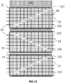
- FIG 13 schematically illustrates an example (top view) of a plurality of photovoltaic plates 10 (three photovoltaic plates 10 in the example shown), with a connection element (divided into a first connection element 21 and a second connection element 22) being provided on a surface of each of the plurality of photovoltaic plates separately, in accordance with an embodiment of the present disclosure.
- a separate connection element 20 is provided (each being divided in a first connection part 21 and a second connection part 22).
- a single connection element 20 may extend over more than one photovoltaic plate 10.
- a single first connection element 21 may extend over two or more neighboring photovoltaic plates
- a single second connection element 22 may extend over two or more neighboring photovoltaic plates.
- the plurality of photovoltaic plates 10 is placed next to each other side by side.
- the plurality of photovoltaic plates 10 is positioned such that a first plate electrode 131 of a photovoltaic plate 10 is located next to a first plate electrode 131 of a neighboring photovoltaic plate and/or such that a second plate electrode 132 of a photovoltaic plate 10 is located next to a second plate electrode 132 of a neighboring photovoltaic plate.
- the present disclosure is not limited thereto, and other ways of positioning or orienting the plurality of photovoltaic plates with respect to each other may be used.
- a dummy element 60 is positioned next to the plurality of photovoltaic plates 10.
- a dummy element 60 may be provided optionally, for example for obtaining a predetermined total size of a photovoltaic module.
- the dummy element 60 may have substantially the same look as the photovoltaic plates 10, for example it may be a piece of a photovoltaic plate (not to be electrically interconnected with the plurality of photovoltaic plates 10) or it may have a look different from the look of the plurality of photovoltaic plates.
- the plurality of plates 10 are schematically shown spaced apart, they maybe positioned closer to each other, e.g. with substantially no spacing therein between, for example to obtain a more uniform global appearance.
- a filling material such as for example a material as used for the electrically insulating layer 40, or for example a silicone material, preferably a material with a visual appearance similar to or substantially equal to the visual appearance of the electrically insulating layer 40, may be provided in spaces between neighboring photovoltaic plates.
- FIG 14 schematically illustrates another example (top view) of a plurality of photovoltaic plates (six photovoltaic plates 10 in the example shown), each having a first connection element 21 and a second connection element 22 being provided on a first surface in accordance with an embodiment of the present disclosure.
- the first connection elements 21 and the second connection elements 22 extend over two neighboring photovoltaic plates 10, the present disclosure not being limited thereto.
- the plurality of photovoltaic plates 10 is arranged side by side, in a two-dimensional array. This is only an example, and other arrangements of the plurality of photovoltaic plates may be used, for example for obtaining a predetermined size and/or a predetermined shape of a thin film photovoltaic module to be fabricated.
- the plurality of photovoltaic plates 10 is electrically interconnected in parallel, the present disclosure not being limited thereto.
- the plurality of photovoltaic plates 10 may be electrically interconnected in series or a combination of series and parallel interconnections may be used.
- the photovoltaic plates 10 may be arranged in a two-dimensional array (as for example schematically illustrated in FIG 14 ) different approaches may be used for establishing a parallel electrical interconnection of the plurality of photovoltaic plates 10.
- the photovoltaic plates 10 arranged in a single 'row' (corresponding to the X-direction indicated in FIG 14 ) of plates may have a same orientation, i.e. their first plate electrodes 131 may be located next to each other in each other's extension and their second plate electrodes 132 may be located next to each other in each other's extension.
- connection element 20 may be used for the photovoltaic plates 10 that are arranged in a same 'row' of plates 10, the connection element 20 extending over at least two, e.g. over all photovoltaic plates 10 in the row.
- a first electrical connection may be formed between the first connection part 21 and the first plate electrodes 131 of the photovoltaic plates arranged in a row
- a second electrical connection may be formed between the second connection part 22 and the second plate electrodes 132 of the photovoltaic plates arranged in the row.
- FIG 14 This is schematically illustrated in FIG 14 . However, this is only an example and the present disclosure is not limited thereto.
- step 104 a first electrical connection is formed for each thin film photovoltaic plate 10 between its first plate electrode 131 and the corresponding first electrically conductive wires 31 (or in other words: between the first plate electrode 131 and the corresponding first connection part 21), i.e. between the first plate electrode and the first electrically conductive wires of the first connection part being provided on the thin film photovoltaic plate.
- step 105 a second electrical connection is formed for each thin film photovoltaic plate 10 between its second electrode 132 and the corresponding second electrically conductive wires 32 (or in other words: between the second electrode 132 and the corresponding second connection part 22), i.e.
- Establishing a first electrical connection and/or a second electrical connection may comprise soldering, welding, gluing, pressing and/or printing, the present disclosure not being limited thereto.
- Step 106 ( FIG 1 ) of a method 100 comprises providing a first electrically conductive busbar of the first polarity and a second electrically conductive busbar of the second polarity. This is followed by forming ( FIG 1 , step 107) for each of the plurality of thin film photovoltaic plates 10 a first electrical busbar connection between the corresponding first electrically conductive wires 21 and the first busbar and forming ( FIG 1 , step 107) for each of the plurality of thin film photovoltaic plates 10 a second electrical busbar connection between the corresponding second electrically conductive wires 22 and the second busbar.
- providing the first busbar and the second busbar may for example comprise providing a first encapsulation sheet, such as a for example a glass sheet, having formed on a surface thereof a first busbar and a second busbar at predetermined locations.
- FIG 15 schematically illustrates an example of a first encapsulation sheet 50 (top view) having a first busbar 61 and a second busbar 62 provided thereon, as may be used in a method according to embodiments of the present disclosure.
- the plurality of photovoltaic plates 10 may be positioned on the first encapsulation sheet 50 as for example schematically illustrated in FIG 16 for a configuration corresponding to the photovoltaic plate arrangement shown in FIG 13 .
- FIG 17 schematically illustrates an embodiment wherein a plurality of photovoltaic plates is arranged in accordance with the configuration shown in FIG 14 and positioned on a first encapsulation sheet 50 containing a first busbar 61 and a second busbar 62.
- At least one first electrically conductive wire 31 may be positioned on (aligned with) the corresponding first busbar 61 and/or at least one second electrically conductive wire 32 may be positioned on (aligned with) the corresponding second busbar 62, for example to allow forming a first electrical busbar connection and/or a second electrical busbar connection by direct soldering, welding, gluing or pressing.
- a first connection element 21 may be positioned non-aligned with the first busbar 61 and/or a second connection element 22 may be positioned non-aligned with the second busbar 62 after their separation.
- forming a first electrical busbar connection and/or forming a second electrical busbar connection may for example comprise providing an electrically conductive structure such as an electrically conductive strip or an electrically conductive grid in between, the present disclosure not being limited thereto.
- this may comprise for example attaching an electrically conductive structure by soldering, welding, gluing or pressing, the present disclosure not being limited thereto.
- this may comprise for example depositing an electrically conductive structure, such as for example by printing a patterned layer comprising an electrically conductive ink, such as for example by means of ink jet printing or screen printing, the present disclosure not being limited thereto.
- an electrically conductive structure may be provided for forming a first electrical busbar connection between at least one first electrically conductive wire 31 and the first busbar 61 and/or forming a second electrical busbar connection between at least one second electrically conductive wire 32 and the second busbar 62.
- the first busbar 61 and the second busbar 62 may for example comprise or consist of an electrically conductive rod, e.g. a full, solid rod or a hollow rod, an electrically conductive strip or an electrically conductive wire, the present disclosure not being limited thereto.
- the first busbar 61 and the second busbar 62 comprise an electrically conductive material, preferably a metal such as for example Al or Cu, the present disclosure not being limited thereto, preferably coated with a solderable material or a weldable material.
- the first busbar 61 and the second busbar 62 are provided to enable further, external electrical connections of a photovoltaic module comprising the plurality of photovoltaic plates 10 according to an embodiment of the third aspect of the present disclosure, to another element such as for example another photovoltaic module.
- the first busbar 61 and/or the second busbar comprise or consist of an electrically conductive rod
- the first and/or second busbar may further have a mechanical function, e.g. they may reinforce the photovoltaic module.
- the present disclosure relates to a method for manufacturing a thin film photovoltaic module.
- An example of a method 200 according to an embodiment of the second aspect of the present disclosure is schematically illustrated in FIG 2 .
- the method 200 comprises: providing ( FIG 2 , step 201) a plurality of thin film photovoltaic plates comprising a first plate electrode of a first polarity and a second plate electrode of a second polarity opposite to the first polarity; providing ( FIG 2 , step 202) a first encapsulation sheet, e.g.
- FIG 2 , step 203 electrically interconnecting ( FIG 2 , step 203) the plurality of thin film photovoltaic plates by a method 100 according to an embodiment in accordance with the first aspect of the present disclosure, wherein providing ( FIG 1 , step 106) the first busbar of the first polarity and the second busbar of the second polarity comprises providing the first busbar and the second busbar on the first encapsulation sheet and wherein positioning ( FIG 1 , step 101) the plurality of thin film photovoltaic plates next to each other side by side comprises positioning the plurality of thin film photovoltaic plates on the first encapsulation sheet, thereby leaving the first busbar and the second busbar exposed; providing ( FIG 2 , step 204) a second encapsulation sheet, e.g.
- the first encapsulation sheet may correspond to a back encapsulation sheet of the photovoltaic module and the second encapsulation sheet may correspond to a front encapsulation sheet of the photovoltaic module or, vice versa, the first encapsulation sheet may correspond to a front encapsulation sheet of the photovoltaic module and the second encapsulation sheet may correspond to a rear encapsulation sheet of the photovoltaic module.
- electrically interconnecting the plurality of thin film photovoltaic plates is performed in accordance with a method 100 according to the first aspect of the present disclosure, wherein providing ( FIG 1 step 106) the first busbar of the first polarity and the second busbar of the second polarity comprises providing ( FIG 2 step 106) the first busbar and the second busbar on a first encapsulation sheet, as described above and as for example illustrated in FIG 16 and FIG 17 , and wherein positioning ( FIG 1 step 101) the plurality of thin film photovoltaic plates next to each other side by side comprises positioning ( FIG 2 step 101) the plurality of thin film photovoltaic plates on the first encapsulation sheet having the first busbar and the second busbar provided thereon, thereby leaving the first busbar and the second busbar exposed, as described above and as for example illustrated in FIG 16 and FIG 17 .
- a method according to embodiments of the second aspect of the present disclosure may further comprise providing an encapsulation layer comprising an encapsulation material (encapsulant) in between the plurality of thin film photovoltaic plates and at least one of the first encapsulation sheet and the second encapsulation sheet.
- an encapsulation layer comprising an encapsulation material (encapsulant) in between the plurality of thin film photovoltaic plates and at least one of the first encapsulation sheet and the second encapsulation sheet.
- the substrate 11 of the photovoltaic plates 10 may have the function of a first or second encapsulation sheet.
- the first busbar 61 and the second busbar 62 may for example be provided on a supporting substrate, such as for example on an electrically insulating foil. Such embodiments may lead to cheaper, thinner and/or lighter photovoltaic modules and to a reduced module cost.
- the plurality of photovoltaic plates 10 within a photovoltaic module is preferably electrically interconnected in parallel, the present disclosure not being limited thereto.
- an encapsulant encapsulation layer, such as for example a layer comprising EVA, PVB, Polyolefin or a silicone
- an encapsulant may be provided on the plurality of thin film photovoltaic plates, preferably fully covering the surface of the plurality of thin film photovoltaic plates. This may be followed by a lamination step to thereby attach the second encapsulation sheet to the plurality of photovoltaic plates, with the encapsulation material therein between.
- the lamination step typically comprises heating, to induce flowing of the encapsulation material.
- this heating step may simultaneously result in the formation of first electrical connections and/or second electrical connections and/or first electrical busbar connections and/or second electrical busbar connections, for example by soldering.
- performing the heating process may comprise performing a first heating step at a first temperature and afterwards performing a second heating step at a second temperature, the second temperature being higher than the first temperature.
- the first temperature may be selected to enable soldering, to thereby form first electrical connections and/or second electrical connections and/or first electrical busbar connections and/or second electrical busbar connections.
- the second temperature may be selected to enable melting of the encapsulation material.
- the first temperature may be in the range between 120°C and 240°C and the second temperature may be 10°C to 50°C higher than the first temperature, the present disclosure not being limited thereto.
- the three steps of providing a connection element 20, providing an electrically insulating layer 40, and providing an encapsulation layer may be combined into two steps or into a single step.
- an electrically insulating layer 40 may be provided on the plurality of photovoltaic plates 10.
- an encapsulation layer having a connection element 20 attached thereto or integrated therewith may be provided on the electrically insulating layer 40.
- separating the connection element 20 into a first connection part 21 and a second connection part 22 may be done before attaching it to or integrating it with the encapsulation layer.
- separating the connection element 20 into a first connection part 21 and a second connection part 22 may be done after attaching it to or integrating it with the encapsulation layer.
- connection element 20 is integrated with or attached to a carrier, such as an encapsulation layer or for example an encapsulation sheet, that it may ease processing and handling of the connection element 20 and/or it may improve its dimensional stability.
- a carrier such as an encapsulation layer or for example an encapsulation sheet
- the electrically insulating layer 40 and the connection element 20 may be combined, i.e. the connection element 20 may be attached to or integrated with the electrically insulating layer 40 before their positioning on the plurality of photovoltaic plates, as described above in relation to an embodiment according to the first aspect of the present disclosure.
- the electrically insulating layer 40, the connection element 20 and a layer of encapsulation material may be combined into a single structure (e.g. a single sheet) before their positioning on the plurality of photovoltaic plates 10.
- the electrically insulating layer 40 and the encapsulation material may be different layers or they may be formed by a single layer, i.e. the electrically insulating layer 40 may also be used as an encapsulant.
- connection element 20 may be provided on the second encapsulation sheet.
- a connection element 20 maybe provided on a surface of the plurality of photovoltaic plates 10 at a side corresponding to the side of the photovoltaic cells 15 (i.e. the side opposite to the side of the substrate 11).
- a connection element 20 may be provided on a surface of the plurality of photovoltaic plates corresponding to the side of the substrate 11. In such embodiments there may be no need for providing an electrically insulating layer 40; in such embodiments an electrical insulation between the connection element and the cell electrodes may be established by the photovoltaic plate substrate 11 located in between.
- Such electrically conductive paths may for example be formed by providing an electrically conductive strip or grid over a lateral edge of the substrate 11 or by printing or depositing a patterned layer comprising an electrically conductive material on a lateral edge of the substrate 11.
- part of the plurality of photovoltaic plates 10 may have a connection element 20 provided on a front surface and another part of the plurality of photovoltaic plates 10 may have a connection element 20 provided on a rear surface.
- a thin film photovoltaic module according to embodiments of the third aspect of the present disclosure comprises: a plurality of thin film photovoltaic plates positioned next to each other side by side, each of the thin film photovoltaic plates comprising a first plate electrode of a first polarity and a second plate electrode of a second polarity opposite to the first polarity; for each of the plurality of thin film photovoltaic plates, a connection element comprising a plurality of electrically conductive wires arranged in a grid structure and divided into a first connection part comprising a plurality of first electrically conductive wires and a second connection part comprising a plurality of second electrically conductive wires, the plurality of first electrically conductive wires being electrically insulated from the plurality of second electrically conductive wires; for each of the plurality of thin film photovoltaic plates, a first electrical connection between corresponding first electrically conductive wires and the first plate electrode and
- a thin film photovoltaic module may be encapsulated, i.e. it may further comprise a front sheet, a back sheet, a front side encapsulation layer and/or a rear side encapsulation layer. It may further comprise a sealing layer and a suitable frame along edges of the module.
Landscapes
- Photovoltaic Devices (AREA)
- Life Sciences & Earth Sciences (AREA)
- Sustainable Development (AREA)
Priority Applications (5)
| Application Number | Priority Date | Filing Date | Title |
|---|---|---|---|
| EP17154742.5A EP3358630B1 (fr) | 2017-02-06 | 2017-02-06 | Panneaux photovoltaïques partiellement translucides et leurs procédés de fabrication |
| RU2019127537A RU2019127537A (ru) | 2017-02-06 | 2018-02-05 | Частично просвечивающиеся фотогальванические модули и способы производства |
| PCT/EP2018/052838 WO2018141976A1 (fr) | 2017-02-06 | 2018-02-05 | Modules photovoltaïques partiellement translucides et procédés de fabrication |
| CN201880010228.5A CN110313072B (zh) | 2017-02-06 | 2018-02-05 | 部分半透明光伏模块以及用于制造的方法 |
| US16/481,605 US10978601B2 (en) | 2017-02-06 | 2018-02-05 | Partially translucent photovoltaic modules and methods for manufacturing |
Applications Claiming Priority (1)
| Application Number | Priority Date | Filing Date | Title |
|---|---|---|---|
| EP17154742.5A EP3358630B1 (fr) | 2017-02-06 | 2017-02-06 | Panneaux photovoltaïques partiellement translucides et leurs procédés de fabrication |
Publications (2)
| Publication Number | Publication Date |
|---|---|
| EP3358630A1 true EP3358630A1 (fr) | 2018-08-08 |
| EP3358630B1 EP3358630B1 (fr) | 2020-04-15 |
Family
ID=57965812
Family Applications (1)
| Application Number | Title | Priority Date | Filing Date |
|---|---|---|---|
| EP17154742.5A Active EP3358630B1 (fr) | 2017-02-06 | 2017-02-06 | Panneaux photovoltaïques partiellement translucides et leurs procédés de fabrication |
Country Status (5)
| Country | Link |
|---|---|
| US (1) | US10978601B2 (fr) |
| EP (1) | EP3358630B1 (fr) |
| CN (1) | CN110313072B (fr) |
| RU (1) | RU2019127537A (fr) |
| WO (1) | WO2018141976A1 (fr) |
Cited By (2)
| Publication number | Priority date | Publication date | Assignee | Title |
|---|---|---|---|---|
| EP3648173A1 (fr) * | 2018-10-30 | 2020-05-06 | IMEC vzw | Module photovoltaïque à film mince comprenant des composants électroniques intégrés et procédés de fabrication de celui-ci |
| CN114664973A (zh) * | 2021-12-28 | 2022-06-24 | 同享(苏州)电子材料科技股份有限公司 | 一种铜包铝反光汇流条的制备方法和光伏组件 |
Families Citing this family (7)
| Publication number | Priority date | Publication date | Assignee | Title |
|---|---|---|---|---|
| JP2020053616A (ja) * | 2018-09-28 | 2020-04-02 | 株式会社リコー | 太陽電池モジュール |
| WO2020247759A1 (fr) * | 2019-06-06 | 2020-12-10 | Grouphug, Inc. | Panneau solaire d'intérieur monté sur fenêtre |
| CN212967720U (zh) * | 2020-09-08 | 2021-04-13 | 东方日升(常州)新能源有限公司 | 一种太阳能电池金属电极结构及电池组件 |
| WO2024204139A1 (fr) * | 2023-03-29 | 2024-10-03 | 株式会社カネカ | Module de cellules solaires |
| CN116913980B (zh) * | 2023-06-07 | 2024-08-09 | 新源劲吾(北京)科技有限公司 | 一种打印的导光图形彩色光伏板及其制作方法 |
| WO2025022532A1 (fr) * | 2023-07-24 | 2025-01-30 | 株式会社東芝 | Structure de cellule solaire connectée |
| CN120187118B (zh) * | 2025-04-07 | 2025-09-26 | 江苏学文新能源有限公司 | 一种光伏组件用层压设备及层压方法 |
Citations (5)
| Publication number | Priority date | Publication date | Assignee | Title |
|---|---|---|---|---|
| DE102008043833A1 (de) * | 2008-11-18 | 2010-05-27 | Q-Cells Se | Solarzellensystem, Solarzellenmodul und Verfahren zur elektrischen Verschaltung rückseitenkontaktierter Solarzellen |
| US20110290296A1 (en) * | 2010-05-27 | 2011-12-01 | Palo Alto Research Center Incorporated | Flexible tiled photovoltaic module |
| EP2660878A1 (fr) * | 2012-05-04 | 2013-11-06 | Sol Invictus Energy | Matières tissées hybrides utiles dans la production de cellules solaires à contact arrière |
| US20150340529A1 (en) * | 2012-12-18 | 2015-11-26 | Commissariat à l'Energie Atomique et aux Energies Alternatives | Device for interconnecting photovoltaic cells having contacts on their back side, and module comprising such a device |
| US20160322526A1 (en) * | 2013-12-20 | 2016-11-03 | Fraunhofer-Gesellschaft zur Förderung der angewandten Forschung e.V. | Photovoltaic cell, photovoltaic module as well as the production and use thereof |
Family Cites Families (26)
| Publication number | Priority date | Publication date | Assignee | Title |
|---|---|---|---|---|
| US4590327A (en) * | 1984-09-24 | 1986-05-20 | Energy Conversion Devices, Inc. | Photovoltaic device and method |
| US4633033A (en) * | 1985-02-08 | 1986-12-30 | Energy Conversion Devices, Inc. | Photovoltaic device and method |
| DE69410536T2 (de) * | 1993-06-24 | 1998-11-26 | Canon K.K., Tokio/Tokyo | Solarmodul mit warm-verschweisstem Teil zur Verbesserung der Feuchtigkeitsbeständigkeit |
| US6175075B1 (en) * | 1998-04-21 | 2001-01-16 | Canon Kabushiki Kaisha | Solar cell module excelling in reliability |
| US20030148024A1 (en) * | 2001-10-05 | 2003-08-07 | Kodas Toivo T. | Low viscosity precursor compositons and methods for the depositon of conductive electronic features |
| JP2000269531A (ja) * | 1999-01-14 | 2000-09-29 | Canon Inc | 太陽電池モジュール、太陽電池モジュール付き建材、太陽電池モジュール外囲体及び太陽光発電装置 |
| US20140102502A1 (en) * | 2006-04-13 | 2014-04-17 | Daniel Luch | Collector grid and interconnect structures for photovoltaic arrays and modules |
| JP2002083990A (ja) * | 2000-07-06 | 2002-03-22 | Canon Inc | 光起電力素子集合体及びそれを用いた太陽電池モジュールと太陽電池モジュールの製造方法 |
| EP2251911B1 (fr) * | 2002-10-25 | 2017-11-29 | Nakajima Glass Co., Inc. | Méthode de fabrication d'un module de cellules solaire |
| US6966184B2 (en) * | 2002-11-25 | 2005-11-22 | Canon Kabushiki Kaisha | Photovoltaic power generating apparatus, method of producing same and photovoltaic power generating system |
| JP2005150318A (ja) * | 2003-11-14 | 2005-06-09 | Canon Inc | 太陽電池モジュール及びその製造方法 |
| JP4681806B2 (ja) * | 2003-12-19 | 2011-05-11 | キヤノン株式会社 | 太陽電池モジュール |
| US20080223429A1 (en) * | 2004-08-09 | 2008-09-18 | The Australian National University | Solar Cell (Sliver) Sub-Module Formation |
| JP5025135B2 (ja) * | 2006-01-24 | 2012-09-12 | 三洋電機株式会社 | 光起電力モジュール |
| JP2008282926A (ja) * | 2007-05-09 | 2008-11-20 | Sanyo Electric Co Ltd | 太陽電池モジュール |
| JP2009088203A (ja) * | 2007-09-28 | 2009-04-23 | Sanyo Electric Co Ltd | 太陽電池、太陽電池モジュール及び太陽電池の製造方法 |
| JP2009135338A (ja) * | 2007-11-30 | 2009-06-18 | Sanyo Electric Co Ltd | 太陽電池及び太陽電池の製造方法 |
| US20090229596A1 (en) * | 2008-03-12 | 2009-09-17 | Myung-Hun Shin | Solar energy module having repair line, solar energy assembly having the same, method of repairing the solar energy module and method of trimming the solar energy assembly |
| US8569613B1 (en) * | 2008-09-29 | 2013-10-29 | Stion Corporation | Multi-terminal photovoltaic module including independent cells and related system |
| KR101656118B1 (ko) * | 2009-09-18 | 2016-09-08 | 파나소닉 아이피 매니지먼트 가부시키가이샤 | 태양 전지, 태양 전지 모듈 및 태양 전지 시스템 |
| KR100990116B1 (ko) * | 2010-05-17 | 2010-10-29 | 엘지전자 주식회사 | 태양전지 모듈 |
| CN101980372A (zh) * | 2010-09-26 | 2011-02-23 | 常州天合光能有限公司 | 具有高反光栅线的太阳电池 |
| JP2013033819A (ja) * | 2011-08-01 | 2013-02-14 | Jx Nippon Oil & Energy Corp | 太陽電池モジュール及びその製造方法 |
| US20130133714A1 (en) * | 2011-11-30 | 2013-05-30 | Primestar Solar, Inc. | Three Terminal Thin Film Photovoltaic Module and Their Methods of Manufacture |
| FR3025944B1 (fr) * | 2014-09-11 | 2017-11-24 | Saint Gobain | Support electroconducteur pour dispositif electrochromique, dispositif electrochromique l'incorporant, et sa fabrication. |
| EP3096360A1 (fr) * | 2015-05-20 | 2016-11-23 | Lg Electronics Inc. | Cellule solaire et module de cellule solaire |
-
2017
- 2017-02-06 EP EP17154742.5A patent/EP3358630B1/fr active Active
-
2018
- 2018-02-05 US US16/481,605 patent/US10978601B2/en active Active
- 2018-02-05 WO PCT/EP2018/052838 patent/WO2018141976A1/fr not_active Ceased
- 2018-02-05 CN CN201880010228.5A patent/CN110313072B/zh active Active
- 2018-02-05 RU RU2019127537A patent/RU2019127537A/ru not_active Application Discontinuation
Patent Citations (5)
| Publication number | Priority date | Publication date | Assignee | Title |
|---|---|---|---|---|
| DE102008043833A1 (de) * | 2008-11-18 | 2010-05-27 | Q-Cells Se | Solarzellensystem, Solarzellenmodul und Verfahren zur elektrischen Verschaltung rückseitenkontaktierter Solarzellen |
| US20110290296A1 (en) * | 2010-05-27 | 2011-12-01 | Palo Alto Research Center Incorporated | Flexible tiled photovoltaic module |
| EP2660878A1 (fr) * | 2012-05-04 | 2013-11-06 | Sol Invictus Energy | Matières tissées hybrides utiles dans la production de cellules solaires à contact arrière |
| US20150340529A1 (en) * | 2012-12-18 | 2015-11-26 | Commissariat à l'Energie Atomique et aux Energies Alternatives | Device for interconnecting photovoltaic cells having contacts on their back side, and module comprising such a device |
| US20160322526A1 (en) * | 2013-12-20 | 2016-11-03 | Fraunhofer-Gesellschaft zur Förderung der angewandten Forschung e.V. | Photovoltaic cell, photovoltaic module as well as the production and use thereof |
Cited By (4)
| Publication number | Priority date | Publication date | Assignee | Title |
|---|---|---|---|---|
| EP3648173A1 (fr) * | 2018-10-30 | 2020-05-06 | IMEC vzw | Module photovoltaïque à film mince comprenant des composants électroniques intégrés et procédés de fabrication de celui-ci |
| CN111200031A (zh) * | 2018-10-30 | 2020-05-26 | Imec 非营利协会 | 具有集成电子器件的薄膜光伏模块及其制造方法 |
| CN111200031B (zh) * | 2018-10-30 | 2024-03-12 | Imec 非营利协会 | 具有集成电子器件的薄膜光伏模块及其制造方法 |
| CN114664973A (zh) * | 2021-12-28 | 2022-06-24 | 同享(苏州)电子材料科技股份有限公司 | 一种铜包铝反光汇流条的制备方法和光伏组件 |
Also Published As
| Publication number | Publication date |
|---|---|
| US20200006585A1 (en) | 2020-01-02 |
| US10978601B2 (en) | 2021-04-13 |
| RU2019127537A (ru) | 2021-03-09 |
| EP3358630B1 (fr) | 2020-04-15 |
| CN110313072A (zh) | 2019-10-08 |
| WO2018141976A1 (fr) | 2018-08-09 |
| CN110313072B (zh) | 2023-05-26 |
Similar Documents
| Publication | Publication Date | Title |
|---|---|---|
| US10978601B2 (en) | Partially translucent photovoltaic modules and methods for manufacturing | |
| US8153889B2 (en) | Roll-to-roll integration of thin film solar modules | |
| EP3544060B1 (fr) | Ensemble de stratification photovoltaïque avec diodes de dérivation | |
| CN102694037B (zh) | 连接器电极,太阳电池模块和电连接多个太阳电池的方法 | |
| US20190027625A1 (en) | Interconnected photovoltaic module configuration | |
| CN110246919A (zh) | 包含搭叠光伏瓦片的光伏模块及其制造工艺 | |
| US11996799B2 (en) | Method for making photovoltaic slats for photovoltaic blinds | |
| KR20140003691A (ko) | 태양 전지 모듈 및 이에 적용되는 리본 결합체 | |
| JP2011523211A (ja) | 背面接点を有するモノリシック集積薄膜太陽電池 | |
| CN105164816A (zh) | 光伏互连系统、装置和方法 | |
| JP5901773B2 (ja) | 直列接続部を含む薄膜ソーラーモジュール、及び、複数の薄膜ソーラーセルを直列接続する方法 | |
| US12484335B2 (en) | Designable shingled photovoltaic module and manufacturing method therefor | |
| EP2816609B1 (fr) | Cellule solaire | |
| US20130146128A1 (en) | Solar cell module | |
| EP3648173B1 (fr) | Module photovoltaïque à film mince comprenant des composants électroniques intégrés et procédés de fabrication de celui-ci | |
| KR102122567B1 (ko) | 확장성을 가진 유연 박막 태양전지 및 그 제조 방법 | |
| KR20140095658A (ko) | 태양 전지 | |
| KR20200017007A (ko) | 2이상의 태양전지 셀을 포함하는 태양전지 셀 스트링 및 그의 제조방법 | |
| KR102398002B1 (ko) | 태양 전지 및 이를 포함하는 태양 전지 패널 | |
| US20120240980A1 (en) | Interconnection Schemes for Photovoltaic Cells | |
| CN118053931A (zh) | 太阳能电池及其制造方法、光伏组件 | |
| TW201214727A (en) | Photovoltaic module including transparent sheet with channel | |
| KR102379388B1 (ko) | 태양 전지 및 이를 포함하는 태양 전지 패널 | |
| KR20160029515A (ko) | 태양 전지 모듈 및 이에 사용되는 리본 | |
| US20200007073A1 (en) | Solar roof tile module with embedded inter-tile circuitry |
Legal Events
| Date | Code | Title | Description |
|---|---|---|---|
| PUAI | Public reference made under article 153(3) epc to a published international application that has entered the european phase |
Free format text: ORIGINAL CODE: 0009012 |
|
| STAA | Information on the status of an ep patent application or granted ep patent |
Free format text: STATUS: THE APPLICATION HAS BEEN PUBLISHED |
|
| AK | Designated contracting states |
Kind code of ref document: A1 Designated state(s): AL AT BE BG CH CY CZ DE DK EE ES FI FR GB GR HR HU IE IS IT LI LT LU LV MC MK MT NL NO PL PT RO RS SE SI SK SM TR |
|
| AX | Request for extension of the european patent |
Extension state: BA ME |
|
| STAA | Information on the status of an ep patent application or granted ep patent |
Free format text: STATUS: REQUEST FOR EXAMINATION WAS MADE |
|
| 17P | Request for examination filed |
Effective date: 20190121 |
|
| RBV | Designated contracting states (corrected) |
Designated state(s): AL AT BE BG CH CY CZ DE DK EE ES FI FR GB GR HR HU IE IS IT LI LT LU LV MC MK MT NL NO PL PT RO RS SE SI SK SM TR |
|
| GRAP | Despatch of communication of intention to grant a patent |
Free format text: ORIGINAL CODE: EPIDOSNIGR1 |
|
| STAA | Information on the status of an ep patent application or granted ep patent |
Free format text: STATUS: GRANT OF PATENT IS INTENDED |
|
| INTG | Intention to grant announced |
Effective date: 20191216 |
|
| GRAS | Grant fee paid |
Free format text: ORIGINAL CODE: EPIDOSNIGR3 |
|
| GRAA | (expected) grant |
Free format text: ORIGINAL CODE: 0009210 |
|
| STAA | Information on the status of an ep patent application or granted ep patent |
Free format text: STATUS: THE PATENT HAS BEEN GRANTED |
|
| AK | Designated contracting states |
Kind code of ref document: B1 Designated state(s): AL AT BE BG CH CY CZ DE DK EE ES FI FR GB GR HR HU IE IS IT LI LT LU LV MC MK MT NL NO PL PT RO RS SE SI SK SM TR |
|
| REG | Reference to a national code |
Ref country code: CH Ref legal event code: EP |
|
| REG | Reference to a national code |
Ref country code: DE Ref legal event code: R096 Ref document number: 602017014615 Country of ref document: DE |
|
| REG | Reference to a national code |
Ref country code: IE Ref legal event code: FG4D |
|
| REG | Reference to a national code |
Ref country code: AT Ref legal event code: REF Ref document number: 1258309 Country of ref document: AT Kind code of ref document: T Effective date: 20200515 |
|
| REG | Reference to a national code |
Ref country code: NL Ref legal event code: MP Effective date: 20200415 |
|
| REG | Reference to a national code |
Ref country code: LT Ref legal event code: MG4D |
|
| PG25 | Lapsed in a contracting state [announced via postgrant information from national office to epo] |
Ref country code: PT Free format text: LAPSE BECAUSE OF FAILURE TO SUBMIT A TRANSLATION OF THE DESCRIPTION OR TO PAY THE FEE WITHIN THE PRESCRIBED TIME-LIMIT Effective date: 20200817 Ref country code: NL Free format text: LAPSE BECAUSE OF FAILURE TO SUBMIT A TRANSLATION OF THE DESCRIPTION OR TO PAY THE FEE WITHIN THE PRESCRIBED TIME-LIMIT Effective date: 20200415 Ref country code: NO Free format text: LAPSE BECAUSE OF FAILURE TO SUBMIT A TRANSLATION OF THE DESCRIPTION OR TO PAY THE FEE WITHIN THE PRESCRIBED TIME-LIMIT Effective date: 20200715 Ref country code: IS Free format text: LAPSE BECAUSE OF FAILURE TO SUBMIT A TRANSLATION OF THE DESCRIPTION OR TO PAY THE FEE WITHIN THE PRESCRIBED TIME-LIMIT Effective date: 20200815 Ref country code: SE Free format text: LAPSE BECAUSE OF FAILURE TO SUBMIT A TRANSLATION OF THE DESCRIPTION OR TO PAY THE FEE WITHIN THE PRESCRIBED TIME-LIMIT Effective date: 20200415 Ref country code: LT Free format text: LAPSE BECAUSE OF FAILURE TO SUBMIT A TRANSLATION OF THE DESCRIPTION OR TO PAY THE FEE WITHIN THE PRESCRIBED TIME-LIMIT Effective date: 20200415 Ref country code: FI Free format text: LAPSE BECAUSE OF FAILURE TO SUBMIT A TRANSLATION OF THE DESCRIPTION OR TO PAY THE FEE WITHIN THE PRESCRIBED TIME-LIMIT Effective date: 20200415 Ref country code: GR Free format text: LAPSE BECAUSE OF FAILURE TO SUBMIT A TRANSLATION OF THE DESCRIPTION OR TO PAY THE FEE WITHIN THE PRESCRIBED TIME-LIMIT Effective date: 20200716 |
|
| REG | Reference to a national code |
Ref country code: AT Ref legal event code: MK05 Ref document number: 1258309 Country of ref document: AT Kind code of ref document: T Effective date: 20200415 |
|
| PG25 | Lapsed in a contracting state [announced via postgrant information from national office to epo] |
Ref country code: LV Free format text: LAPSE BECAUSE OF FAILURE TO SUBMIT A TRANSLATION OF THE DESCRIPTION OR TO PAY THE FEE WITHIN THE PRESCRIBED TIME-LIMIT Effective date: 20200415 Ref country code: BG Free format text: LAPSE BECAUSE OF FAILURE TO SUBMIT A TRANSLATION OF THE DESCRIPTION OR TO PAY THE FEE WITHIN THE PRESCRIBED TIME-LIMIT Effective date: 20200715 Ref country code: RS Free format text: LAPSE BECAUSE OF FAILURE TO SUBMIT A TRANSLATION OF THE DESCRIPTION OR TO PAY THE FEE WITHIN THE PRESCRIBED TIME-LIMIT Effective date: 20200415 Ref country code: HR Free format text: LAPSE BECAUSE OF FAILURE TO SUBMIT A TRANSLATION OF THE DESCRIPTION OR TO PAY THE FEE WITHIN THE PRESCRIBED TIME-LIMIT Effective date: 20200415 |
|
| PG25 | Lapsed in a contracting state [announced via postgrant information from national office to epo] |
Ref country code: AL Free format text: LAPSE BECAUSE OF FAILURE TO SUBMIT A TRANSLATION OF THE DESCRIPTION OR TO PAY THE FEE WITHIN THE PRESCRIBED TIME-LIMIT Effective date: 20200415 |
|
| REG | Reference to a national code |
Ref country code: DE Ref legal event code: R097 Ref document number: 602017014615 Country of ref document: DE |
|
| PG25 | Lapsed in a contracting state [announced via postgrant information from national office to epo] |
Ref country code: RO Free format text: LAPSE BECAUSE OF FAILURE TO SUBMIT A TRANSLATION OF THE DESCRIPTION OR TO PAY THE FEE WITHIN THE PRESCRIBED TIME-LIMIT Effective date: 20200415 Ref country code: AT Free format text: LAPSE BECAUSE OF FAILURE TO SUBMIT A TRANSLATION OF THE DESCRIPTION OR TO PAY THE FEE WITHIN THE PRESCRIBED TIME-LIMIT Effective date: 20200415 Ref country code: CZ Free format text: LAPSE BECAUSE OF FAILURE TO SUBMIT A TRANSLATION OF THE DESCRIPTION OR TO PAY THE FEE WITHIN THE PRESCRIBED TIME-LIMIT Effective date: 20200415 Ref country code: SM Free format text: LAPSE BECAUSE OF FAILURE TO SUBMIT A TRANSLATION OF THE DESCRIPTION OR TO PAY THE FEE WITHIN THE PRESCRIBED TIME-LIMIT Effective date: 20200415 Ref country code: IT Free format text: LAPSE BECAUSE OF FAILURE TO SUBMIT A TRANSLATION OF THE DESCRIPTION OR TO PAY THE FEE WITHIN THE PRESCRIBED TIME-LIMIT Effective date: 20200415 Ref country code: EE Free format text: LAPSE BECAUSE OF FAILURE TO SUBMIT A TRANSLATION OF THE DESCRIPTION OR TO PAY THE FEE WITHIN THE PRESCRIBED TIME-LIMIT Effective date: 20200415 Ref country code: DK Free format text: LAPSE BECAUSE OF FAILURE TO SUBMIT A TRANSLATION OF THE DESCRIPTION OR TO PAY THE FEE WITHIN THE PRESCRIBED TIME-LIMIT Effective date: 20200415 Ref country code: ES Free format text: LAPSE BECAUSE OF FAILURE TO SUBMIT A TRANSLATION OF THE DESCRIPTION OR TO PAY THE FEE WITHIN THE PRESCRIBED TIME-LIMIT Effective date: 20200415 |
|
| PLBE | No opposition filed within time limit |
Free format text: ORIGINAL CODE: 0009261 |
|
| STAA | Information on the status of an ep patent application or granted ep patent |
Free format text: STATUS: NO OPPOSITION FILED WITHIN TIME LIMIT |
|
| PG25 | Lapsed in a contracting state [announced via postgrant information from national office to epo] |
Ref country code: SK Free format text: LAPSE BECAUSE OF FAILURE TO SUBMIT A TRANSLATION OF THE DESCRIPTION OR TO PAY THE FEE WITHIN THE PRESCRIBED TIME-LIMIT Effective date: 20200415 Ref country code: PL Free format text: LAPSE BECAUSE OF FAILURE TO SUBMIT A TRANSLATION OF THE DESCRIPTION OR TO PAY THE FEE WITHIN THE PRESCRIBED TIME-LIMIT Effective date: 20200415 |
|
| 26N | No opposition filed |
Effective date: 20210118 |
|
| PG25 | Lapsed in a contracting state [announced via postgrant information from national office to epo] |
Ref country code: SI Free format text: LAPSE BECAUSE OF FAILURE TO SUBMIT A TRANSLATION OF THE DESCRIPTION OR TO PAY THE FEE WITHIN THE PRESCRIBED TIME-LIMIT Effective date: 20200415 |
|
| PG25 | Lapsed in a contracting state [announced via postgrant information from national office to epo] |
Ref country code: MC Free format text: LAPSE BECAUSE OF FAILURE TO SUBMIT A TRANSLATION OF THE DESCRIPTION OR TO PAY THE FEE WITHIN THE PRESCRIBED TIME-LIMIT Effective date: 20200415 |
|
| GBPC | Gb: european patent ceased through non-payment of renewal fee |
Effective date: 20210206 |
|
| REG | Reference to a national code |
Ref country code: BE Ref legal event code: MM Effective date: 20210228 |
|
| PG25 | Lapsed in a contracting state [announced via postgrant information from national office to epo] |
Ref country code: CH Free format text: LAPSE BECAUSE OF NON-PAYMENT OF DUE FEES Effective date: 20210228 Ref country code: LU Free format text: LAPSE BECAUSE OF NON-PAYMENT OF DUE FEES Effective date: 20210206 Ref country code: LI Free format text: LAPSE BECAUSE OF NON-PAYMENT OF DUE FEES Effective date: 20210228 |
|
| PG25 | Lapsed in a contracting state [announced via postgrant information from national office to epo] |
Ref country code: GB Free format text: LAPSE BECAUSE OF NON-PAYMENT OF DUE FEES Effective date: 20210206 Ref country code: IE Free format text: LAPSE BECAUSE OF NON-PAYMENT OF DUE FEES Effective date: 20210206 |
|
| PG25 | Lapsed in a contracting state [announced via postgrant information from national office to epo] |
Ref country code: BE Free format text: LAPSE BECAUSE OF NON-PAYMENT OF DUE FEES Effective date: 20210228 |
|
| P01 | Opt-out of the competence of the unified patent court (upc) registered |
Effective date: 20230513 |
|
| PG25 | Lapsed in a contracting state [announced via postgrant information from national office to epo] |
Ref country code: CY Free format text: LAPSE BECAUSE OF FAILURE TO SUBMIT A TRANSLATION OF THE DESCRIPTION OR TO PAY THE FEE WITHIN THE PRESCRIBED TIME-LIMIT Effective date: 20200415 |
|
| PG25 | Lapsed in a contracting state [announced via postgrant information from national office to epo] |
Ref country code: HU Free format text: LAPSE BECAUSE OF FAILURE TO SUBMIT A TRANSLATION OF THE DESCRIPTION OR TO PAY THE FEE WITHIN THE PRESCRIBED TIME-LIMIT; INVALID AB INITIO Effective date: 20170206 |
|
| PG25 | Lapsed in a contracting state [announced via postgrant information from national office to epo] |
Ref country code: MK Free format text: LAPSE BECAUSE OF FAILURE TO SUBMIT A TRANSLATION OF THE DESCRIPTION OR TO PAY THE FEE WITHIN THE PRESCRIBED TIME-LIMIT Effective date: 20200415 |
|
| PG25 | Lapsed in a contracting state [announced via postgrant information from national office to epo] |
Ref country code: TR Free format text: LAPSE BECAUSE OF FAILURE TO SUBMIT A TRANSLATION OF THE DESCRIPTION OR TO PAY THE FEE WITHIN THE PRESCRIBED TIME-LIMIT Effective date: 20200415 |
|
| PG25 | Lapsed in a contracting state [announced via postgrant information from national office to epo] |
Ref country code: MT Free format text: LAPSE BECAUSE OF FAILURE TO SUBMIT A TRANSLATION OF THE DESCRIPTION OR TO PAY THE FEE WITHIN THE PRESCRIBED TIME-LIMIT Effective date: 20200415 |
|
| REG | Reference to a national code |
Ref country code: DE Ref legal event code: R079 Ref document number: 602017014615 Country of ref document: DE Free format text: PREVIOUS MAIN CLASS: H01L0031050000 Ipc: H10F0019900000 |
|
| PGFP | Annual fee paid to national office [announced via postgrant information from national office to epo] |
Ref country code: DE Payment date: 20260121 Year of fee payment: 10 |
|
| PGFP | Annual fee paid to national office [announced via postgrant information from national office to epo] |
Ref country code: FR Payment date: 20260121 Year of fee payment: 10 |