EP3358683B1 - Elektrische steckkupplungsvorrichtung in deren gehäuse ein elektronisches bauteil angeordnet ist. - Google Patents
Elektrische steckkupplungsvorrichtung in deren gehäuse ein elektronisches bauteil angeordnet ist. Download PDFInfo
- Publication number
- EP3358683B1 EP3358683B1 EP17154824.1A EP17154824A EP3358683B1 EP 3358683 B1 EP3358683 B1 EP 3358683B1 EP 17154824 A EP17154824 A EP 17154824A EP 3358683 B1 EP3358683 B1 EP 3358683B1
- Authority
- EP
- European Patent Office
- Prior art keywords
- housing
- electrical plug
- coupling apparatus
- electronic component
- layer thickness
- Prior art date
- Legal status (The legal status is an assumption and is not a legal conclusion. Google has not performed a legal analysis and makes no representation as to the accuracy of the status listed.)
- Active
Links
Images

Classifications
-
- H—ELECTRICITY
- H10—SEMICONDUCTOR DEVICES; ELECTRIC SOLID-STATE DEVICES NOT OTHERWISE PROVIDED FOR
- H10W—GENERIC PACKAGES, INTERCONNECTIONS, CONNECTORS OR OTHER CONSTRUCTIONAL DETAILS OF DEVICES COVERED BY CLASS H10
- H10W40/00—Arrangements for thermal protection or thermal control
- H10W40/70—Fillings or auxiliary members in containers or in encapsulations for thermal protection or control
-
- H—ELECTRICITY
- H05—ELECTRIC TECHNIQUES NOT OTHERWISE PROVIDED FOR
- H05K—PRINTED CIRCUITS; CASINGS OR CONSTRUCTIONAL DETAILS OF ELECTRIC APPARATUS; MANUFACTURE OF ASSEMBLAGES OF ELECTRICAL COMPONENTS
- H05K5/00—Casings, cabinets or drawers for electric apparatus
- H05K5/02—Details
- H05K5/0256—Details of interchangeable modules or receptacles therefor, e.g. cartridge mechanisms
- H05K5/026—Details of interchangeable modules or receptacles therefor, e.g. cartridge mechanisms having standardized interfaces
- H05K5/0278—Details of interchangeable modules or receptacles therefor, e.g. cartridge mechanisms having standardized interfaces of USB type
-
- H—ELECTRICITY
- H05—ELECTRIC TECHNIQUES NOT OTHERWISE PROVIDED FOR
- H05K—PRINTED CIRCUITS; CASINGS OR CONSTRUCTIONAL DETAILS OF ELECTRIC APPARATUS; MANUFACTURE OF ASSEMBLAGES OF ELECTRICAL COMPONENTS
- H05K7/00—Constructional details common to different types of electric apparatus
- H05K7/20—Modifications to facilitate cooling, ventilating, or heating
- H05K7/2039—Modifications to facilitate cooling, ventilating, or heating characterised by the heat transfer by conduction from the heat generating element to a dissipating body
- H05K7/20436—Inner thermal coupling elements in heat dissipating housings, e.g. protrusions or depressions integrally formed in the housing
- H05K7/20445—Inner thermal coupling elements in heat dissipating housings, e.g. protrusions or depressions integrally formed in the housing the coupling element being an additional piece, e.g. thermal standoff
- H05K7/20454—Inner thermal coupling elements in heat dissipating housings, e.g. protrusions or depressions integrally formed in the housing the coupling element being an additional piece, e.g. thermal standoff with a conformable or flexible structure compensating for irregularities, e.g. cushion bags, thermal paste
-
- H—ELECTRICITY
- H10—SEMICONDUCTOR DEVICES; ELECTRIC SOLID-STATE DEVICES NOT OTHERWISE PROVIDED FOR
- H10W—GENERIC PACKAGES, INTERCONNECTIONS, CONNECTORS OR OTHER CONSTRUCTIONAL DETAILS OF DEVICES COVERED BY CLASS H10
- H10W40/00—Arrangements for thermal protection or thermal control
- H10W40/20—Arrangements for cooling
- H10W40/22—Arrangements for cooling characterised by their shape, e.g. having conical or cylindrical projections
- H10W40/226—Arrangements for cooling characterised by their shape, e.g. having conical or cylindrical projections characterised by projecting parts, e.g. fins to increase surface area
- H10W40/228—Arrangements for cooling characterised by their shape, e.g. having conical or cylindrical projections characterised by projecting parts, e.g. fins to increase surface area the projecting parts being wire-shaped or pin-shaped
Definitions
- the invention relates to an electrical plug-in coupling device according to claim 1, which is particularly suitable as part of a prefabricated cable for transmitting electrical currents, for example for charging accumulators.
- the electrical plug-in coupling devices in question can be used, for example, in connection with cables in motor vehicles or aircraft and are usually required in large numbers. A simple construction and simple assembly of the electrical plug-in coupling devices are of great importance for the cost-effective provision of corresponding cables.
- efforts are underway to integrate electronic circuits, in particular electronic components on printed circuit boards, into the plug-in coupling devices.
- electronic circuits can be designed as charging electronics for charging accumulators which are connected to the electrical plug-in coupling devices. It is important that the plug-in coupling devices are not thermally stressed too much by the waste heat generated within the plug-in coupling devices.
- EP 2 916 636 A1 discloses an electronic device having a housing with an opening. A metal body is placed in the opening to dissipate the heat.
- a plug-in coupling device which has a housing which is made from thermally conductive polymer material for dissipating heat.
- the invention has for its object to provide an electrical plug-in coupling device which is protected against excessive self-heating and yet can be manufactured with relatively little production effort.
- the electrical plug-in coupling device comprises a housing and a printed circuit board.
- the housing in turn comprises a plastic part with a pocket.
- the plastic part has an inner surface and a outer surface.
- a first metal layer is applied at least to the outer surface.
- the circuit board is arranged in the housing and equipped with at least one electronic component.
- the first metal layer has a first layer thickness in a first surface area and a second layer thickness in a second surface area.
- the second surface area is arranged in the pocket and the second layer thickness is greater than the first layer thickness.
- the electronic component is arranged in the housing in such a way that it is thermally connected to the second surface area, in particular without an air gap, and a straight line with an orthogonal course relative to the printed circuit board intersects both the electronic component and the second surface area.
- pocket is to be understood in the following in particular as a depression, a recess or a recess in the geometry of the housing or the plastic part.
- the distance between the circuit board and the outer surface of the plastic part in the region of the pocket is smaller than in a region of the plastic part adjacent to the pocket. So the distance between the circuit board and the second area is smaller than the distance between the circuit board and the first area.
- the inner surface of the plastic part of the housing is to be understood in particular as the surface which is directed towards the printed circuit board or whose surface normal points towards the printed circuit board.
- the outer surface accordingly faces outwards in relation to the housing.
- the first layer thickness of the first metal layer in the first surface area is advantageously between 20 ⁇ m and 30 ⁇ m and the second layer thickness in the second surface area is between 25 ⁇ m and 40 ⁇ m.
- the second layer thickness is advantageously at least 1.1 times larger than the first layer thickness, in a particularly advantageous manner at least 1.25 times larger than the first layer thickness or at least 1.3 times larger than the first layer thickness.
- the electronic component is in particular thermally connected to the second surface area such that the thermal resistance between the electronic component and the second surface area is less than 30 K / W, in particular less than 20 K / W, advantageously less than 8 K / W.
- a second metal layer is applied to the inner surface of the housing in a third area, which is arranged such that the straight line also intersects the third area.
- the electronic component is thermally connected to the inner surface of the housing in the third surface area without an air gap.
- a thermal paste is advantageously arranged between the electronic component and the inner surface of the housing for the thermal connection of the electronic component.
- the electronic component can directly touch the inner surface of the housing, with this Design, in particular, the contact can be generated by a mechanical bias between the housing and the electronic component.
- the housing has a recess which is filled with thermally conductive material, which is arranged such that the straight line intersects the thermally conductive material.
- the electrical plug-in coupling device is designed such that the thermally conductive material completely penetrates the plastic part.
- the first and / or the second metal layer can in particular be applied galvanically.
- the first metal layer can be applied galvanically, while the second metal layer is attached to the plastic part as a plate.
- the electrical plug-in coupling device is advantageously designed such that the second surface area runs parallel to the printed circuit board.
- the third surface area runs (also) parallel to the printed circuit board.
- the invention is particularly advantageous if the electronic component is a voltage regulator by means of which an input voltage can be regulated to a lower output voltage, in particular for charging an accumulator that can be connected to the plug-in coupling device.
- the electronic component is a voltage regulator by means of which an input voltage can be regulated to a lower output voltage, in particular for charging an accumulator that can be connected to the plug-in coupling device.
- it is necessary to dissipate considerable amounts of heat loss to the environment in order to avoid overheating of the plug-in coupling device, in particular of the voltage regulator.
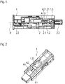
- the electrical plug coupling device described in the presented exemplary embodiment comprises a flat printed circuit board 2 according to FIG Figure 1 .
- 2 contacts 2.2 are arranged or mounted on the printed circuit board.
- the orientation of the contacts 2.2 is such that the plug connection in question can be established or released parallel to an axis X as intended.
- the contacts 2.2 are electrically connected to a circuit which includes an electronic component 2.1, the component 2.1 being arranged on the printed circuit board 2 or the printed circuit board 2 being equipped with the electronic component 2.2.
- the circuit board 2 comprises an input contact 2.3, which can be connected to lines of a cable.
- the plug-in coupling device is in particular designed such that it is designed as a charging socket for charging an accumulator of a terminal.
- the electronic component 2.1 is designed as a voltage regulator which, for example, regulates the voltage of an electrical system of a motor vehicle down to an output voltage of approximately 5 V. In this process, heat loss is released.
- the electrical plug-in coupling device comprises a housing 1 according to the Figure 2 , in which the circuit board 2 with the electronic component 2.1 is arranged.
- the housing 1 comprises a plastic part 1.3 which has an outer surface and an inner surface, a first metal layer 1.1 being applied at least to the outer surface and a second metal layer 1.2 being applied to the inner surface, in particular by means of a galvanizing process ( Figure 3 ).
- metal plates can also be installed here.
- the plastic part 1.3 has a pocket 1.31.
- the distance y between the printed circuit board 2 or its surface and the outer surface of the plastic part 1.3 in the area of the pocket 1.31 is smaller than the distance Y in an area of the plastic part 1.3 adjacent to the pocket 1.31.
- the first metal layer 1.1 on the outer surface has a first surface area A1 and a second surface area A2, the second surface area A2 being arranged in the pocket 1.31 parallel to the printed circuit board 2.
- the first metal layer 1.1 has a first layer thickness d1 in the first surface area A1 and a second layer thickness d2 in the second surface area A2.
- the second layer thickness d2 is greater than the first layer thickness d1.
- the second metal layer 1.2 has a third surface area A3 on the inner surface, the second metal layer 1.2 here having a thickness of 25 ⁇ m.
- thermal paste 3 is applied to the electronic component 2.1.
- a straight line g which runs orthogonal relative to the printed circuit board 2, intersects both the electronic component 2.1 and the second surface area A2.
- straight line g also runs orthogonal to axis X.
- the thermal paste 3 contacts the electronic component 2.1 and the second metal layer 1.2 of the inner surface in the third surface area A3.
- the plastic part 1.3 has a comparatively thin wall thickness, in particular in the area of the pocket 1.31, heat can flow with relatively little thermal resistance between the second metal layer 1.2 on the inner surface and the first metal layer 1.1 on the outer surface, in particular between the third surface area A3 and the second surface area A2.
- the plastic part 1.3 can have an increased thermal conductivity, for example by adding thermally conductive fillers into the starting material of the plastic part 1.3.
- the electronic component 2.1 is arranged in the housing 1 such that it is thermally connected to the second surface area A2 without an air gap.
- the electrical plug-in coupling device is connected to an electrical line, so that a prefabricated cable is produced.
- Such cables are usually used to transmit electrical energy.
- the cable is particularly intended for installation in a vehicle and, according to the exemplary embodiment, is intended for charging an external battery, for example in a mobile device.
- the electronic component 2.1 During operation of the plug-in coupling device, the electronic component 2.1 generates heat loss, which essentially flows via the thermally conductive thermal paste 3 to the second metal layer 1.2 on the inner surface. As a result, the first metal layer 1.1 is heated in the second surface area A2 on the outer surface. On the one hand, the second surface area A2 gives off part of the heat directly to the surroundings and another part of the heat to the first surface area A1 of the first metal layer 1.1, via which heat then flows off to the surroundings.
- a housing 1 ' has a plastic part 1.3' with a recess.
- the recess is filled with thermally conductive material 4, for example by a coating process or in the form of a steel, aluminum or copper rivet.
- the plastic part 1.3 ′ designed in this way is subjected to a coating process, so that the first metal layer 1.1 is formed on its outer surface, which is essentially analogous to that of the first exemplary embodiment and accordingly also has two surface areas A1, A2 of different thicknesses d1, d2.
- the thermally conductive material 4 is arranged such that the straight line g also intersects it.
- the heat loss generated by the electronic component 2.1 flows via the thermal paste 3 to the thermally conductive material 4 and then into the second surface area A2 of the first metal layer 1.1 on the outer surface of the housing 1 ′, in particular the pocket 1.31.
Landscapes
- Engineering & Computer Science (AREA)
- Microelectronics & Electronic Packaging (AREA)
- Physics & Mathematics (AREA)
- Thermal Sciences (AREA)
- Cooling Or The Like Of Electrical Apparatus (AREA)
Description
- Die Erfindung betrifft eine elektrische Steckkupplungsvorrichtung gemäß dem Anspruch 1, welche insbesondere als Teil eines konfektionierten Kabels zur Übertragung von elektrischen Strömen, beispielsweise zum Aufladen von Ackumulatoren, geeignet ist.
- Die betreffenden elektrischen Steckkupplungsvorrichtungen sind etwa im Zusammenhang mit Kabeln in Kraftfahrzeugen oder Luftfahrzeugen einsetzbar und werden meist in großen Stückzahlen benötigt. Zur kostengünstigen Bereitstellung entsprechender Kabel sind ein einfacher Aufbau und eine einfache Konfektionierbarkeit der elektrischen Steckkupplungsvorrichtungen von großer Bedeutung. Andererseits sind Bestrebungen im Gange, dass in die Steckkupplungsvorrichtungen elektronische Schaltungen, insbesondere elektronische Bauteile auf Leiterplatten, integriert werden. Beispielsweise können derartige Schaltungen als Ladeelektronik ausgestaltet sein zum Aufladen von Akkumulatoren, die mit der elektrischen Steckkupplungsvorrichtungen verbunden sind. Es ist wichtig, dass die Steckkupplungsvorrichtungen durch die innerhalb der Steckkupplungsvorrichtungen erzeugte Abwärme thermisch nicht zu stark belastet werden.
- Die Offenlegungsschrift
EP 2 916 636 A1 offenbart eine elektronische Vorrichtung, die ein Gehäuse mit einer Öffnung aufweist. Zur Ableitung der Wärme wird in der Öffnung ein Metallkörper platziert. - Im Dokument
EP 2 003 741 A1 wird eine Steckeranordnung beschrieben, die thermoplastische Halbschalen mit einer Nickelbeschichtung aufweist. Auf diese Weise soll eine geschirmte Subminiatur-Verbindungsbaugruppe erhalten werden. - In der
US 2016/0192541 A1 wird ein Gehäuse für eine elektronische Vorrichtung gezeigt, bei der die Abwärme von elektronischen Bauteilen ausdrücklich nicht zu den Wänden des Gehäuses übertragen wird. Vielmehr wird dort die Abwärme über ein so genanntes dissipation board aus Metall, das in einer Öffnung des Gehäuses angeordnet ist, direkt an die Umgebung abgegeben. - Zudem ist in der Offenlegungsschrift
US 2016/0329672 A1 ein Stecker zum Aufladen von elektronischen Geräten offenbart, wobei der Stecker in seinem Gehäuse eine Leiterplatte mit elektronischen Bauteilen aufweist. - Aus der Patentschrift
US 6851869 B2 ist eine Steckkupplungsvorrichtung bekannt, die ein Gehäuse aufweist, welches zur Ableitung von Wärme aus thermisch leitfähigem Polymer-Material hergestellt ist. - Der Erfindung liegt die Aufgabe zugrunde, eine elektrische Steckkupplungsvorrichtung zu schaffen, welche vor übermäßiger Eigenerwärmung geschützt ist und dennoch mit relativ geringem Herstellungsaufwand fertigbar ist.
- Diese Aufgabe wird erfindungsgemäß durch die Merkmale des Anspruches 1 gelöst.
- Erfindungsgemäß umfasst die elektrische Steckkupplungsvorrichtung ein Gehäuse und eine Leiterplatte. Das Gehäuse umfasst seinerseits ein Kunststoffteil mit einer Tasche. Das Kunststoffteil weist eine innere Oberfläche und eine äußere Oberfläche auf. Zumindest an der äußeren Oberfläche ist eine erste Metallschicht aufgebracht. Die Leiterplatte ist im Gehäuse angeordnet und mit zumindest einem elektronischen Bauteil bestückt. Die erste Metallschicht weist in einem ersten Flächenbereich eine erste Schichtdicke und in einem zweiten Flächenbereich eine zweite Schichtdicke auf. Der zweite Flächenbereich ist in der Tasche angeordnet und die zweite Schichtdicke ist größer als die erste Schichtdicke. Das elektronische Bauteil ist so im Gehäuse angeordnet, dass dieses insbesondere ohne Luftspalt mit dem zweiten Flächenbereich thermisch verbunden ist und eine Gerade mit relativ zur Leiterplatte orthogonalem Verlauf sowohl das elektronische Bauteil als auch den zweiten Flächenbereich schneidet.
- Unter dem Begriff Tasche ist im Folgenden insbesondere eine Mulde, eine Eintiefung oder ein Rücksprung in der Geometrie des Gehäuses beziehungsweise des Kunststoffteils zu verstehen. Mit anderen Worten ausgedrückt ist der Abstand zwischen der Leiterplatte und der äußeren Oberfläche des Kunststoffteils im Bereich der Tasche kleiner als in einem der Tasche benachbarten Bereich des Kunststoffteils. Somit ist der Abstand zwischen der Leiterplatte und dem zweiten Flächenbereich kleiner als der Abstand zwischen Leiterplatte und dem ersten Flächenbereich.
- Als innere Oberfläche des Kunststoffteils des Gehäuses ist insbesondere diejenige Oberfläche zu verstehen, die zur Leiterplatte hin gerichtete ist, beziehungsweise dessen Flächennormale zur Leiterplatte weist. Die äußere Oberfläche weist demgemäß bezogen auf das Gehäuse nach außen.
- Mit Vorteil beträgt die erste Schichtdicke der ersten Metallschicht im ersten Flächenbereich zwischen 20 µm und 30 µm und die zweite Schichtdicke im zweiten Flächenbereich zwischen 25 µm und 40 µm.
- Mit Vorteil ist die zweite Schichtdicke mindestens 1,1-mal größer als die erste Schichtdicke in besonders vorteilhafterweise mindestens 1,25-mal größer als die erste Schichtdicke oder mindestens 1,3-mal größer als die erste Schichtdicke.
- Das elektronische Bauteil ist insbesondere derart mit dem zweiten Flächenbereich thermisch verbunden, dass der Wärmewiderstand zwischen dem elektronischen Bauteil und dem zweiten Flächenbereich kleiner ist als 30 K/W, insbesondere kleiner als 20 K/W, mit Vorteil kleiner als 8 K/W.
- In vorteilhafter Bauweise ist an der inneren Oberfläche des Gehäuses in einem dritten Flächenbereich eine zweite Metallschicht aufgebracht, welche so angeordnet ist, dass die Gerade auch den dritten Flächenbereich schneidet.
- In weiterer Ausgestaltung der Erfindung ist das elektronische Bauteil ohne Luftspalt mit der inneren Oberfläche des Gehäuses im dritten Flächenbereich thermisch verbunden.
- Mit Vorteil ist zur thermischen Anbindung des elektronischen Bauteils eine Wärmeleitpaste zwischen dem elektronischen Bauteil und der inneren Oberfläche des Gehäuses angeordnet. Alternativ kann das elektronische Bauteil unmittelbar die innere Oberfläche des Gehäuses berühren, wobei bei dieser Ausgestaltung insbesondere die Berührung durch eine mechanische Vorspannung zwischen dem Gehäuse und dem elektronischen Bauteil erzeugt werden kann.
- In vorteilhafter Bauweise weist das Gehäuse eine Ausnehmung auf, die mit thermisch leitfähigem Material ausgefüllt ist, welches so angeordnet ist, dass die Gerade das thermisch leitfähige Material schneidet.
- In weiterer Ausgestaltung der Erfindung ist die elektrische Steckkupplungsvorrichtung so ausgebildet, dass das thermisch leitfähige Material das Kunststoffteil vollständig durchdringt.
- Die erste und / oder die zweite Metallschicht kann insbesondere galvanisch aufgebracht sein. Insbesondere kann die erste Metallschicht galvanisch aufgebracht sein, während die zweite Metallschicht als Plättchen am Kunststoffteil befestigt ist.
- Mit Vorteil ist die elektrische Steckkupplungsvorrichtung so ausgebildet, dass der zweite Flächenbereich parallel zur Leiterplatte verläuft.
- In weiterer Ausgestaltung der Erfindung verläuft (auch) der dritte Flächenbereich parallel zur Leiterplatte.
- Besonders vorteilhaft ist die Erfindung, wenn das elektronische Bauteil ein Spannungsregler ist, durch den eine Eingangsspannung auf eine niedrigere Ausgangsspannung regelbar ist, insbesondere zum Laden eines an die Steckkupplungsvorrichtung anschließbaren Akkumulators. Gerade in diesem Fall ist es erforderlich erhebliche Mengen an Verlustwärme an die Umgebung abzuführen um eine Überhitzung der Steckkupplungsvorrichtung insbesondere des Spannungsreglers zu vermeiden.
- Vorteilhafte Ausbildungen der Erfindung entnimmt man den abhängigen Ansprüchen.
- Weitere Einzelheiten und Vorteile der erfindungsgemäßen Steckkupplungsvorrichtung ergeben sich aus der nachfolgenden Beschreibung von Ausführungsbeispielen anhand der beiliegenden Figuren.
- Es zeigen die
- Figur 1
- eine Längsschnittdarstellung einer Steckkupplungsvorrichtung,
- Figur 2
- eine perspektivische Ansicht der Steckkupplungsvorrichtung,
- Figur 3
- eine Detailansicht der Steckkupplungsvorrichtung in einer Schnittdarstellung,
- Figur 4
- eine Detailansicht der Steckkupplungsvorrichtung in einer Schnittdarstellung nach einem zweiten Ausführungsbeispiel.
- Die im vorgestellten Ausführungsbeispiel beschriebene elektrische Stecckupplungsvorrichtung umfasst eine ebene Leiterplatte 2 gemäß der
Figur 1 . Zur Herstellung einer elektrischen Verbindung mit einem Gegenstück der Steckkupplungsvorrichtung sind an der Leiterplatte 2 Kontakte 2.2 angeordnet beziehungsweise montiert. Die Orientierung der Kontakte 2.2 ist derart, dass ein Herstellen oder Lösen der betreffenden Steckverbindung parallel zu einer Achse X bestimmungsgemäß erfolgen kann. Die Kontakte 2.2 sind elektrisch mit einer Schaltung verbunden, die unter anderem ein elektronisches Bauteil 2.1 umfasst, wobei das Bauteil 2.1 auf der Leiterplatte 2 angeordnet ist beziehungsweise die Leiterplatte 2 mit dem elektronischen Bauteil 2.2 bestückt ist. Weiterhin umfasst die Leiterplatte 2 einen Eingangskontakt 2.3, welcher mit Leitungen eines Kabels verbindbar ist. Die Steckkupplungsvorrichtung ist insbesondere so ausgestaltet, dass dieses als Ladebuchse zum Aufladen eines Akkumulators eines Endgerätes ausgebildet ist. Demgemäß ist das elektronische Bauteil 2.1 als Spannungsregler ausgebildet, der beispielsweise die Spannung eines Bordnetzes eines Kraftfahrzeuges auf einen Ausgangsspannung von etwa 5 V herunterregelt. Bei diesem Vorgang wird Verlustwärme frei. - Ferner umfasst die elektrische Steckkupplungsvorrichtung ein Gehäuse 1 gemäß der
Figur 2 , in welchem die Leiterplatte 2 mit dem elektronischen Bauteil 2.1 angeordnet ist. - Das Gehäuse 1 umfasst ein Kunststoffteil 1.3, das eine äußere Oberfläche und eine innere Oberfläche aufweist, wobei zumindest an der äußeren Oberfläche eine erste Metallschicht 1.1 und an der inneren Oberfläche eine zweite Metallschicht 1.2, insbesondere durch einen Galvanisierungsprozess, aufgebracht ist (
Figur 3 ). Alternativ können hier auch Metallplättchen montiert werden. - Weiterhin weist das Kunststoffteil 1.3 eine Tasche 1.31 auf. Der Abstand y zwischen der Leiterplatte 2 beziehungsweise deren Oberfläche und der äußeren Oberfläche des Kunststoffteils 1.3 im Bereich der Tasche 1.31 ist kleiner als der Abstand Y in einem der Tasche 1.31 benachbarten Bereich des Kunststoffteils 1.3.
- Die erste Metallschicht 1.1 auf der äußeren Oberfläche weist einen ersten Flächenbereich A1 und einen zweiten Flächenbereich A2 auf, wobei der zweite Flächenbereich A2 in der Tasche 1.31 parallel zur Leiterplatte 2 angeordnet ist. Die erste Metallschicht 1.1 weist im ersten Flächenbereich A1 eine erste Schichtdicke d1 und im zweiten Flächenbereich A2 eine zweite Schichtdicke d2 auf. Die zweite Schichtdicke d2 ist größer als die erste Schichtdicke d1. Im vorgestellten Ausführungsbeispiel beträgt die erste Schichtdicke d1 = 20 µm und die zweite Schichtdicke d2 = 25 µm (d2/d1 = 1,25).
- Gemäß der
Figur 3 weist die zweite Metallschicht 1.2 auf der inneren Oberfläche einen dritten Flächenbereich A3 auf, wobei hier die zweite Metallschicht 1.2 eine Dicke von 25 µm aufweist. Vor dem Zusammenbau der Steckkupplungsvorrichtung wird auf das elektronische Bauteil 2.1 Wärmeleitpaste 3 aufgetragen. Im zusammengebauten Zustand liegt eine Anordnung vor, bei der eine Gerade g, die relativ zur Leiterplatte 2 orthogonal verläuft, sowohl das elektronische Bauteil 2.1 als auch den zweiten Flächenbereich A2 schneidet. Im vorgestellten Ausführungsbeispiel verläuft im Übrigen die Gerade g auch orthogonal zu Achse X. Weiterhin berührt die Wärmeleitpaste 3 das elektronische Bauteil 2.1 und die zweite Metallschicht 1.2 der inneren Oberfläche im dritten Flächenbereich A3. Dadurch dass, das Kunststoffteil 1.3 insbesondere im Bereich der Tasche 1.31 eine vergleichsweise dünne Wandstärke aufweist, kann Wärme mit relativ wenig thermischen Widerstand zwischen der zweiten Metallschicht 1.2 auf der inneren Oberfläche zur ersten Metallschicht 1.1 auf der äußeren Oberfläche fließen, insbesondere zwischen dem dritten Flächenbereich A3 und dem zweiten Flächenbereich A2. Zur Verminderung des Wärmedurchlasswiderstandes kann das Kunststoffteil 1.3 eine erhöhte Wärmeleitfähigkeit aufweisen, beispielsweise durch Zugabe von thermisch leitfähigen Füllstoffen in das Ausgangsmaterial des Kunststoffteils 1.3. - Im Ergebnis ist im vorgestellten Ausführungsbeispiel das elektronische Bauteil 2.1 so im Gehäuse 1 angeordnet, dass dieses ohne Luftspalt mit dem zweiten Flächenbereich A2 thermisch verbunden ist.
- Die elektrische Steckkupplungsvorrichtung wird bestimmungsgemäß mit einer elektrischen Leitung verbunden, so dass ein konfektioniertes Kabel hergestellt ist. Derartige Kabel dienen üblicherweise zur Übertragung von elektrischer Energie. Das Kabel ist insbesondere zum Einbau in einem Fahrzeug bestimmt und ist gemäß dem Ausführungsbeispiel zum Laden eines externen Akkus, etwa in einem mobilen Gerät, bestimmt.
- Im Betrieb der Steckkupplungsvorrichtung erzeugt das elektronische Bauteil 2.1 Verlustwärme, die im Wesentlichen über die thermisch leitfähige Wärmeleitpaste 3 zur zweiten Metallschicht 1.2 auf der inneren Oberfläche fließt. Dadurch wird auf der äußeren Oberfläche die erste Metallschicht 1.1 im zweiten Flächenbereich A2 erwärmt. Der zweite Flächenbereich A2 gibt einerseits einen Teil der Wärme unmittelbar an die Umgebung ab und einen anderen Teil der Wärme an den ersten Flächenbereich A1 der ersten Metallschicht 1.1, über den dann wiederum Wärme an die Umgebung abfließt.
- Auf diese Weise kann eine übermäßige thermische Belastung der Leiterplatte 2 beziehungsweise des elektronischen Bauteils 2.1 vermieden werden.
- Gemäß der
Figur 4 ist ein zweites Ausführungsbeispiel beschrieben. Dort weist ein Gehäuse 1' ein Kunststoffteil 1.3' mit einer Ausnehmung auf. Die Ausnehmung ist mit thermisch leitfähigem Material 4 ausgefüllt, beispielsweise durch einen Beschichtungsprozess oder in Form eines Stahl-, Aluminium- oder Kupferniets. Das so ausgestaltete Kunststoffteil 1.3' wird einem Beschichtungsprozess unterworfen, so dass wiederum an dessen äußeren Oberfläche die erste Metallschicht 1.1 entsteht, die im Wesentlichen analog zu derjenigen des ersten Ausführungsbeispiels ausgestaltet ist und demnach auch zwei Flächenbereiche A1, A2 unterschiedlicher Dicke d1, d2 aufweist. - Das thermisch leitfähige Material 4 ist so angeordnet, dass die Gerade g auch dieses schneidet. Somit fließt in diesem Ausführungsbeispiel die vom elektronischen Bauteil 2.1 erzeugte Verlustwärme über die Wärmeleitpaste 3 zum thermisch leitfähigen Material 4 und dann in den zweiten Flächenbereich A2 der ersten Metallschicht 1.1 auf der äußeren Oberfläche des Gehäuses 1', insbesondere der Tasche 1.31.
Claims (15)
- Elektrische Steckkupplungsvorrichtung umfassend ein Gehäuse (1; 1') und eine Leiterplatte (2), wobei- das Gehäuse (1; 1') ein Kunststoffteil (1.3; 1.3') umfasst, das eine innere Oberfläche und eine äußere Oberfläche aufweist,- die Leiterplatte (2) mit zumindest einem elektronischen Bauteil (2.1) bestückt ist und im Gehäuse angeordnet ist,- wobei das Gehäuse (1; 1') eine Tasche (1.31) aufweist,
dadurch gekennzeichnet, dass
das Kunststoffteil (1.3; 1.3') des Gehäuses (1; 1') die Tasche (1.31) aufweist, wobei zumindest an der äußeren Oberfläche eine erste Metallschicht (1.1) aufgebracht ist, die- in einem ersten Flächenbereich (A1) eine erste Schichtdicke (d1) und- in einem zweiten Flächenbereich (A2), der in der Tasche (1.31) angeordnet ist, eine zweite Schichtdicke (d2) aufweist, wobei
die zweite Schichtdicke (d2) größer ist als die erste Schichtdicke (d1) und das elektronische Bauteil (2.1) so im Gehäuse (1; 1') angeordnet ist, dass dieses mit dem zweiten Flächenbereich (A2) thermisch verbunden ist und eine Gerade (g) mit relativ zur Leiterplatte (2) orthogonalem Verlauf sowohl das elektronische Bauteil (2.1) als auch den zweiten Flächenbereich (A2) schneidet. - Elektrische Steckkupplungsvorrichtung gemäß dem Anspruch 1, wobei an der inneren Oberfläche des Gehäuses (1; 1') in einem dritten Flächenbereich (A3) eine zweite Metallschicht (1.2) aufgebracht ist, welche so angeordnet ist, dass die Gerade (g) auch den dritten Flächenbereich (A3) schneidet.
- Elektrische Steckkupplungsvorrichtung gemäß dem Anspruch 2, wobei das elektronische Bauteil (2.1) ohne Luftspalt mit der inneren Oberfläche des Gehäuses (1; 1') im dritten Flächenbereich (A3) thermisch verbunden ist.
- Elektrische Steckkupplungsvorrichtung gemäß einem der vorhergehenden Ansprüche, wobei zur thermischen Anbindung des elektronischen Bauteils (2.1) eine Wärmeleitpaste (3) zwischen dem elektronischen Bauteil (2.1) und der inneren Oberfläche des Gehäuses (1; 1') angeordnet ist.
- Elektrische Steckkupplungsvorrichtung gemäß einem der vorhergehenden Ansprüche, wobei das Gehäuse (1') eine Ausnehmung aufweist, die mit thermisch leitfähigem Material (4) ausgefüllt ist, welches so angeordnet ist, dass die Gerade (g) auch dieses schneidet.
- Elektrische Steckkupplungsvorrichtung gemäß dem Anspruch 5, wobei das thermisch leitfähige Material (4) das Kunststoffteil (1.3') vollständig durchdringt.
- Elektrische Steckkupplungsvorrichtung gemäß einem der vorhergehenden Ansprüche, wobei die erste Metallschicht (1.1) galvanisch aufgebracht ist.
- Elektrische Steckkupplungsvorrichtung gemäß einem der vorhergehenden Ansprüche, wobei die zweite Metallschicht (1.2) galvanisch aufgebracht ist.
- Elektrische Steckkupplungsvorrichtung gemäß einem der vorhergehenden Ansprüche, wobei der zweite Flächenbereich (A2) parallel zur Leiterplatte (2) verläuft.
- Elektrische Steckkupplungsvorrichtung gemäß einem der vorhergehenden Ansprüche, wobei der dritte Flächenbereich (A3) parallel zur Leiterplatte (2) verläuft.
- Elektrische Steckkupplungsvorrichtung gemäß einem der vorhergehenden Ansprüche, wobei ein Abstand (y) zwischen der Leiterplatte (2) und der äußeren Oberfläche des Kunststoffteils (1.3) im Bereich der Tasche (1.31) kleiner ist als der Abstand (Y) in einem der Tasche (1.31) benachbarten Bereich des Kunststoffteils (1.3).
- Elektrische Steckkupplungsvorrichtung gemäß einem der vorhergehenden Ansprüche, wobei das elektronische Bauteil (2.1) ein Spannungsregler ist, durch den eine Eingangsspannung auf eine niedrigere Ausgangsspannung regelbar ist, insbesondere zum Laden eines an die Steckkupplungsvorrichtung anschließbaren Akkumulators.
- Elektrische Steckkupplungsvorrichtung gemäß einem der vorhergehenden Ansprüche, wobei die erste Schichtdicke (d1) der ersten Metallschicht (1.1) in dem ersten Flächenbereich (A1) zwischen 20 µm und 30 µm und die zweite Schichtdicke (d2) in dem zweiten Flächenbereich (A2) zwischen 25 µm und 40 µm beträgt.
- Elektrische Steckkupplungsvorrichtung gemäß einem der vorhergehenden Ansprüche, wobei die zweite Schichtdicke (d2) mindestens 1,1-mal größer als die erste Schichtdicke (d1) ist.
- Elektrische Steckkupplungsvorrichtung nach Anspruch 14, wobei die zweite Schichtdicke (d2) mindestens 1,25-mal größer ist als die erste Schichtdicke (d1).
Priority Applications (1)
| Application Number | Priority Date | Filing Date | Title |
|---|---|---|---|
| EP17154824.1A EP3358683B1 (de) | 2017-02-06 | 2017-02-06 | Elektrische steckkupplungsvorrichtung in deren gehäuse ein elektronisches bauteil angeordnet ist. |
Applications Claiming Priority (1)
| Application Number | Priority Date | Filing Date | Title |
|---|---|---|---|
| EP17154824.1A EP3358683B1 (de) | 2017-02-06 | 2017-02-06 | Elektrische steckkupplungsvorrichtung in deren gehäuse ein elektronisches bauteil angeordnet ist. |
Publications (2)
| Publication Number | Publication Date |
|---|---|
| EP3358683A1 EP3358683A1 (de) | 2018-08-08 |
| EP3358683B1 true EP3358683B1 (de) | 2020-07-01 |
Family
ID=57984825
Family Applications (1)
| Application Number | Title | Priority Date | Filing Date |
|---|---|---|---|
| EP17154824.1A Active EP3358683B1 (de) | 2017-02-06 | 2017-02-06 | Elektrische steckkupplungsvorrichtung in deren gehäuse ein elektronisches bauteil angeordnet ist. |
Country Status (1)
| Country | Link |
|---|---|
| EP (1) | EP3358683B1 (de) |
Family Cites Families (6)
| Publication number | Priority date | Publication date | Assignee | Title |
|---|---|---|---|---|
| US6851869B2 (en) | 2000-08-04 | 2005-02-08 | Cool Options, Inc. | Highly thermally conductive electronic connector |
| ATE543237T1 (de) * | 2007-06-15 | 2012-02-15 | Souriau | Subminiatur abgeschirmte verbinderanordnung und verfahren zum austatten einer solchen verbinderandordnug. |
| JP2014093414A (ja) * | 2012-11-02 | 2014-05-19 | Hitachi Automotive Systems Ltd | 電子制御装置 |
| DE102012022004B3 (de) * | 2012-11-12 | 2014-02-06 | HARTING Electronics GmbH | Isolierkörper mit Schirmkreuz |
| BR202014032719Y1 (pt) * | 2014-12-26 | 2020-04-07 | Embraco Ind De Compressores E Solucoes Em Refrigeracao Ltda | gabinete de dispositivo eletrônico |
| US20160329672A1 (en) * | 2015-05-04 | 2016-11-10 | James William McGinley | Housing configuration for charger plug |
-
2017
- 2017-02-06 EP EP17154824.1A patent/EP3358683B1/de active Active
Non-Patent Citations (1)
| Title |
|---|
| None * |
Also Published As
| Publication number | Publication date |
|---|---|
| EP3358683A1 (de) | 2018-08-08 |
Similar Documents
| Publication | Publication Date | Title |
|---|---|---|
| EP3478531B1 (de) | Elektroanschlusseinrichtung mit thermischer kopplung einer einen temperatursensor aufweisenden platine | |
| DE112017007934B4 (de) | Anordnung mit einem wasserdichten konnektor und verfahren zum zusammenbau derselben | |
| DE102006018457A1 (de) | Elektronische Schaltungsvorrichtung | |
| DE102013010843A1 (de) | Elektrisches Steuergerät | |
| DE102016216848B4 (de) | Hochfrequenzentladungszündvorrichtung | |
| DE102014203732A1 (de) | Elektronisches teil und elektronische steuereinheit | |
| DE102018104536A1 (de) | Festteil eines steckverbinders | |
| DE102016000843A1 (de) | Kontaktierungssystem für Energiespeicherzellen und Energiespeicher | |
| DE102011076273A1 (de) | Leiterplatte für elektrische Bauelemente und Leiterplattensystem | |
| DE102014216281A1 (de) | Steckverbinder für die Übertragung von Hochvoltstrom im Kfz-Bereich | |
| EP2514285B1 (de) | Abschlusselement für ein gehäuse | |
| DE102015221474A1 (de) | Energiespeichervorrichtung und Verfahren zum Fertigen einer Energiespeichervorrichtung | |
| DE102023119078A1 (de) | Leistungskabelbaum mit Sammelschiene | |
| DE102023104242A1 (de) | Mehrteiliges Steckerbauteil sowie Baugruppe und Kraftfahrzeug damit | |
| EP3358683A1 (de) | Elektrische steckkupplungsvorrichtung in deren gehäuse ein elektronischer bauteil angeordnet ist. | |
| DE102017206146B4 (de) | Hochstrom-Steckbuchse und Hochstrom-Steckeranordnung mit einer Hochstrom-Steckbuchse | |
| DE102010030460A1 (de) | Elektronisches Gerät mit Gehäuse aus Profilmaterial | |
| DE102018113757A1 (de) | Abdeckung für Batteriegehäuse | |
| DE102009026886A1 (de) | Formteil zur Aufnahme mehrerer elektrischer Bauteile | |
| DE102017204395A1 (de) | Elektronische steuereinheit | |
| DE102022117193A1 (de) | Gehäuse für ein elektrisches oder elektronisches Gerät | |
| EP4576441A1 (de) | Elektrische steckverbinderanordnung | |
| DE102024111361A1 (de) | Elektrogerät | |
| DE102016208737A1 (de) | Montageadapter und Leistungsmodulsystem | |
| DE102025108897A1 (de) | Elektromagnetische abschirmboxbaugruppe und elektromechanische vorrichtung |
Legal Events
| Date | Code | Title | Description |
|---|---|---|---|
| STAA | Information on the status of an ep patent application or granted ep patent |
Free format text: STATUS: EXAMINATION IS IN PROGRESS |
|
| PUAI | Public reference made under article 153(3) epc to a published international application that has entered the european phase |
Free format text: ORIGINAL CODE: 0009012 |
|
| 17P | Request for examination filed |
Effective date: 20170206 |
|
| AK | Designated contracting states |
Kind code of ref document: A1 Designated state(s): AL AT BE BG CH CY CZ DE DK EE ES FI FR GB GR HR HU IE IS IT LI LT LU LV MC MK MT NL NO PL PT RO RS SE SI SK SM TR |
|
| AX | Request for extension of the european patent |
Extension state: BA ME |
|
| RBV | Designated contracting states (corrected) |
Designated state(s): AL AT BE BG CH CY CZ DE DK EE ES FI FR GB GR HR HU IE IS IT LI LT LU LV MC MK MT NL NO PL PT RO RS SE SI SK SM TR |
|
| RIN1 | Information on inventor provided before grant (corrected) |
Inventor name: ENGL, RUDOLF Inventor name: BOCK, DANIEL Inventor name: HOFMANN, THOMAS Inventor name: KAASERER, MARKUS Inventor name: HERMES, JENS |
|
| GRAP | Despatch of communication of intention to grant a patent |
Free format text: ORIGINAL CODE: EPIDOSNIGR1 |
|
| STAA | Information on the status of an ep patent application or granted ep patent |
Free format text: STATUS: GRANT OF PATENT IS INTENDED |
|
| GRAS | Grant fee paid |
Free format text: ORIGINAL CODE: EPIDOSNIGR3 |
|
| INTG | Intention to grant announced |
Effective date: 20200428 |
|
| GRAA | (expected) grant |
Free format text: ORIGINAL CODE: 0009210 |
|
| STAA | Information on the status of an ep patent application or granted ep patent |
Free format text: STATUS: THE PATENT HAS BEEN GRANTED |
|
| AK | Designated contracting states |
Kind code of ref document: B1 Designated state(s): AL AT BE BG CH CY CZ DE DK EE ES FI FR GB GR HR HU IE IS IT LI LT LU LV MC MK MT NL NO PL PT RO RS SE SI SK SM TR |
|
| REG | Reference to a national code |
Ref country code: AT Ref legal event code: REF Ref document number: 1287034 Country of ref document: AT Kind code of ref document: T Effective date: 20200715 Ref country code: CH Ref legal event code: EP |
|
| REG | Reference to a national code |
Ref country code: IE Ref legal event code: FG4D Free format text: LANGUAGE OF EP DOCUMENT: GERMAN |
|
| REG | Reference to a national code |
Ref country code: DE Ref legal event code: R096 Ref document number: 502017005920 Country of ref document: DE |
|
| REG | Reference to a national code |
Ref country code: LT Ref legal event code: MG4D |
|
| PG25 | Lapsed in a contracting state [announced via postgrant information from national office to epo] |
Ref country code: BG Free format text: LAPSE BECAUSE OF FAILURE TO SUBMIT A TRANSLATION OF THE DESCRIPTION OR TO PAY THE FEE WITHIN THE PRESCRIBED TIME-LIMIT Effective date: 20201001 |
|
| REG | Reference to a national code |
Ref country code: NL Ref legal event code: MP Effective date: 20200701 |
|
| PG25 | Lapsed in a contracting state [announced via postgrant information from national office to epo] |
Ref country code: HR Free format text: LAPSE BECAUSE OF FAILURE TO SUBMIT A TRANSLATION OF THE DESCRIPTION OR TO PAY THE FEE WITHIN THE PRESCRIBED TIME-LIMIT Effective date: 20200701 Ref country code: FI Free format text: LAPSE BECAUSE OF FAILURE TO SUBMIT A TRANSLATION OF THE DESCRIPTION OR TO PAY THE FEE WITHIN THE PRESCRIBED TIME-LIMIT Effective date: 20200701 Ref country code: CZ Free format text: LAPSE BECAUSE OF FAILURE TO SUBMIT A TRANSLATION OF THE DESCRIPTION OR TO PAY THE FEE WITHIN THE PRESCRIBED TIME-LIMIT Effective date: 20200701 Ref country code: ES Free format text: LAPSE BECAUSE OF FAILURE TO SUBMIT A TRANSLATION OF THE DESCRIPTION OR TO PAY THE FEE WITHIN THE PRESCRIBED TIME-LIMIT Effective date: 20200701 Ref country code: LT Free format text: LAPSE BECAUSE OF FAILURE TO SUBMIT A TRANSLATION OF THE DESCRIPTION OR TO PAY THE FEE WITHIN THE PRESCRIBED TIME-LIMIT Effective date: 20200701 Ref country code: GR Free format text: LAPSE BECAUSE OF FAILURE TO SUBMIT A TRANSLATION OF THE DESCRIPTION OR TO PAY THE FEE WITHIN THE PRESCRIBED TIME-LIMIT Effective date: 20201002 Ref country code: NO Free format text: LAPSE BECAUSE OF FAILURE TO SUBMIT A TRANSLATION OF THE DESCRIPTION OR TO PAY THE FEE WITHIN THE PRESCRIBED TIME-LIMIT Effective date: 20201001 Ref country code: PT Free format text: LAPSE BECAUSE OF FAILURE TO SUBMIT A TRANSLATION OF THE DESCRIPTION OR TO PAY THE FEE WITHIN THE PRESCRIBED TIME-LIMIT Effective date: 20201102 Ref country code: SE Free format text: LAPSE BECAUSE OF FAILURE TO SUBMIT A TRANSLATION OF THE DESCRIPTION OR TO PAY THE FEE WITHIN THE PRESCRIBED TIME-LIMIT Effective date: 20200701 |
|
| PG25 | Lapsed in a contracting state [announced via postgrant information from national office to epo] |
Ref country code: IS Free format text: LAPSE BECAUSE OF FAILURE TO SUBMIT A TRANSLATION OF THE DESCRIPTION OR TO PAY THE FEE WITHIN THE PRESCRIBED TIME-LIMIT Effective date: 20201101 Ref country code: RS Free format text: LAPSE BECAUSE OF FAILURE TO SUBMIT A TRANSLATION OF THE DESCRIPTION OR TO PAY THE FEE WITHIN THE PRESCRIBED TIME-LIMIT Effective date: 20200701 Ref country code: PL Free format text: LAPSE BECAUSE OF FAILURE TO SUBMIT A TRANSLATION OF THE DESCRIPTION OR TO PAY THE FEE WITHIN THE PRESCRIBED TIME-LIMIT Effective date: 20200701 Ref country code: LV Free format text: LAPSE BECAUSE OF FAILURE TO SUBMIT A TRANSLATION OF THE DESCRIPTION OR TO PAY THE FEE WITHIN THE PRESCRIBED TIME-LIMIT Effective date: 20200701 |
|
| PG25 | Lapsed in a contracting state [announced via postgrant information from national office to epo] |
Ref country code: NL Free format text: LAPSE BECAUSE OF FAILURE TO SUBMIT A TRANSLATION OF THE DESCRIPTION OR TO PAY THE FEE WITHIN THE PRESCRIBED TIME-LIMIT Effective date: 20200701 |
|
| REG | Reference to a national code |
Ref country code: DE Ref legal event code: R097 Ref document number: 502017005920 Country of ref document: DE |
|
| PG25 | Lapsed in a contracting state [announced via postgrant information from national office to epo] |
Ref country code: IT Free format text: LAPSE BECAUSE OF FAILURE TO SUBMIT A TRANSLATION OF THE DESCRIPTION OR TO PAY THE FEE WITHIN THE PRESCRIBED TIME-LIMIT Effective date: 20200701 Ref country code: EE Free format text: LAPSE BECAUSE OF FAILURE TO SUBMIT A TRANSLATION OF THE DESCRIPTION OR TO PAY THE FEE WITHIN THE PRESCRIBED TIME-LIMIT Effective date: 20200701 Ref country code: SM Free format text: LAPSE BECAUSE OF FAILURE TO SUBMIT A TRANSLATION OF THE DESCRIPTION OR TO PAY THE FEE WITHIN THE PRESCRIBED TIME-LIMIT Effective date: 20200701 Ref country code: DK Free format text: LAPSE BECAUSE OF FAILURE TO SUBMIT A TRANSLATION OF THE DESCRIPTION OR TO PAY THE FEE WITHIN THE PRESCRIBED TIME-LIMIT Effective date: 20200701 Ref country code: RO Free format text: LAPSE BECAUSE OF FAILURE TO SUBMIT A TRANSLATION OF THE DESCRIPTION OR TO PAY THE FEE WITHIN THE PRESCRIBED TIME-LIMIT Effective date: 20200701 |
|
| PLBE | No opposition filed within time limit |
Free format text: ORIGINAL CODE: 0009261 |
|
| STAA | Information on the status of an ep patent application or granted ep patent |
Free format text: STATUS: NO OPPOSITION FILED WITHIN TIME LIMIT |
|
| PG25 | Lapsed in a contracting state [announced via postgrant information from national office to epo] |
Ref country code: AL Free format text: LAPSE BECAUSE OF FAILURE TO SUBMIT A TRANSLATION OF THE DESCRIPTION OR TO PAY THE FEE WITHIN THE PRESCRIBED TIME-LIMIT Effective date: 20200701 |
|
| 26N | No opposition filed |
Effective date: 20210406 |
|
| PG25 | Lapsed in a contracting state [announced via postgrant information from national office to epo] |
Ref country code: SK Free format text: LAPSE BECAUSE OF FAILURE TO SUBMIT A TRANSLATION OF THE DESCRIPTION OR TO PAY THE FEE WITHIN THE PRESCRIBED TIME-LIMIT Effective date: 20200701 |
|
| PG25 | Lapsed in a contracting state [announced via postgrant information from national office to epo] |
Ref country code: SI Free format text: LAPSE BECAUSE OF FAILURE TO SUBMIT A TRANSLATION OF THE DESCRIPTION OR TO PAY THE FEE WITHIN THE PRESCRIBED TIME-LIMIT Effective date: 20200701 |
|
| PG25 | Lapsed in a contracting state [announced via postgrant information from national office to epo] |
Ref country code: MC Free format text: LAPSE BECAUSE OF FAILURE TO SUBMIT A TRANSLATION OF THE DESCRIPTION OR TO PAY THE FEE WITHIN THE PRESCRIBED TIME-LIMIT Effective date: 20200701 |
|
| GBPC | Gb: european patent ceased through non-payment of renewal fee |
Effective date: 20210206 |
|
| REG | Reference to a national code |
Ref country code: BE Ref legal event code: MM Effective date: 20210228 |
|
| PG25 | Lapsed in a contracting state [announced via postgrant information from national office to epo] |
Ref country code: LI Free format text: LAPSE BECAUSE OF NON-PAYMENT OF DUE FEES Effective date: 20210228 Ref country code: LU Free format text: LAPSE BECAUSE OF NON-PAYMENT OF DUE FEES Effective date: 20210206 Ref country code: CH Free format text: LAPSE BECAUSE OF NON-PAYMENT OF DUE FEES Effective date: 20210228 |
|
| PG25 | Lapsed in a contracting state [announced via postgrant information from national office to epo] |
Ref country code: IE Free format text: LAPSE BECAUSE OF NON-PAYMENT OF DUE FEES Effective date: 20210206 Ref country code: GB Free format text: LAPSE BECAUSE OF NON-PAYMENT OF DUE FEES Effective date: 20210206 |
|
| PG25 | Lapsed in a contracting state [announced via postgrant information from national office to epo] |
Ref country code: BE Free format text: LAPSE BECAUSE OF NON-PAYMENT OF DUE FEES Effective date: 20210228 |
|
| REG | Reference to a national code |
Ref country code: AT Ref legal event code: MM01 Ref document number: 1287034 Country of ref document: AT Kind code of ref document: T Effective date: 20220206 |
|
| PG25 | Lapsed in a contracting state [announced via postgrant information from national office to epo] |
Ref country code: AT Free format text: LAPSE BECAUSE OF NON-PAYMENT OF DUE FEES Effective date: 20220206 |
|
| PG25 | Lapsed in a contracting state [announced via postgrant information from national office to epo] |
Ref country code: CY Free format text: LAPSE BECAUSE OF FAILURE TO SUBMIT A TRANSLATION OF THE DESCRIPTION OR TO PAY THE FEE WITHIN THE PRESCRIBED TIME-LIMIT Effective date: 20200701 |
|
| PG25 | Lapsed in a contracting state [announced via postgrant information from national office to epo] |
Ref country code: HU Free format text: LAPSE BECAUSE OF FAILURE TO SUBMIT A TRANSLATION OF THE DESCRIPTION OR TO PAY THE FEE WITHIN THE PRESCRIBED TIME-LIMIT; INVALID AB INITIO Effective date: 20170206 |
|
| PG25 | Lapsed in a contracting state [announced via postgrant information from national office to epo] |
Ref country code: MK Free format text: LAPSE BECAUSE OF FAILURE TO SUBMIT A TRANSLATION OF THE DESCRIPTION OR TO PAY THE FEE WITHIN THE PRESCRIBED TIME-LIMIT Effective date: 20200701 |
|
| PG25 | Lapsed in a contracting state [announced via postgrant information from national office to epo] |
Ref country code: TR Free format text: LAPSE BECAUSE OF FAILURE TO SUBMIT A TRANSLATION OF THE DESCRIPTION OR TO PAY THE FEE WITHIN THE PRESCRIBED TIME-LIMIT Effective date: 20200701 |
|
| PG25 | Lapsed in a contracting state [announced via postgrant information from national office to epo] |
Ref country code: MT Free format text: LAPSE BECAUSE OF FAILURE TO SUBMIT A TRANSLATION OF THE DESCRIPTION OR TO PAY THE FEE WITHIN THE PRESCRIBED TIME-LIMIT Effective date: 20200701 |
|
| PGFP | Annual fee paid to national office [announced via postgrant information from national office to epo] |
Ref country code: FR Payment date: 20250221 Year of fee payment: 9 |
|
| PGFP | Annual fee paid to national office [announced via postgrant information from national office to epo] |
Ref country code: DE Payment date: 20260218 Year of fee payment: 10 |