EP3364344A1 - Procédé de fabrication d'une incrustation en profondeur pour un film composite d'un document de sécurité et/ou de valeur ainsi qu'incrustation en profondeur - Google Patents
Procédé de fabrication d'une incrustation en profondeur pour un film composite d'un document de sécurité et/ou de valeur ainsi qu'incrustation en profondeur Download PDFInfo
- Publication number
- EP3364344A1 EP3364344A1 EP18152006.5A EP18152006A EP3364344A1 EP 3364344 A1 EP3364344 A1 EP 3364344A1 EP 18152006 A EP18152006 A EP 18152006A EP 3364344 A1 EP3364344 A1 EP 3364344A1
- Authority
- EP
- European Patent Office
- Prior art keywords
- microchip
- film
- recess
- compensating
- adhesive
- Prior art date
- Legal status (The legal status is an assumption and is not a legal conclusion. Google has not performed a legal analysis and makes no representation as to the accuracy of the status listed.)
- Granted
Links
Images

Classifications
-
- G—PHYSICS
- G06—COMPUTING OR CALCULATING; COUNTING
- G06K—GRAPHICAL DATA READING; PRESENTATION OF DATA; RECORD CARRIERS; HANDLING RECORD CARRIERS
- G06K19/00—Record carriers for use with machines and with at least a part designed to carry digital markings
- G06K19/06—Record carriers for use with machines and with at least a part designed to carry digital markings characterised by the kind of the digital marking, e.g. shape, nature, code
- G06K19/067—Record carriers with conductive marks, printed circuits or semiconductor circuit elements, e.g. credit or identity cards also with resonating or responding marks without active components
- G06K19/07—Record carriers with conductive marks, printed circuits or semiconductor circuit elements, e.g. credit or identity cards also with resonating or responding marks without active components with integrated circuit chips
- G06K19/077—Constructional details, e.g. mounting of circuits in the carrier
- G06K19/0772—Physical layout of the record carrier
- G06K19/07728—Physical layout of the record carrier the record carrier comprising means for protection against impact or bending, e.g. protective shells or stress-absorbing layers around the integrated circuit
-
- G—PHYSICS
- G06—COMPUTING OR CALCULATING; COUNTING
- G06K—GRAPHICAL DATA READING; PRESENTATION OF DATA; RECORD CARRIERS; HANDLING RECORD CARRIERS
- G06K19/00—Record carriers for use with machines and with at least a part designed to carry digital markings
- G06K19/06—Record carriers for use with machines and with at least a part designed to carry digital markings characterised by the kind of the digital marking, e.g. shape, nature, code
- G06K19/067—Record carriers with conductive marks, printed circuits or semiconductor circuit elements, e.g. credit or identity cards also with resonating or responding marks without active components
- G06K19/07—Record carriers with conductive marks, printed circuits or semiconductor circuit elements, e.g. credit or identity cards also with resonating or responding marks without active components with integrated circuit chips
- G06K19/077—Constructional details, e.g. mounting of circuits in the carrier
- G06K19/0772—Physical layout of the record carrier
- G06K19/07722—Physical layout of the record carrier the record carrier being multilayered, e.g. laminated sheets
-
- G—PHYSICS
- G06—COMPUTING OR CALCULATING; COUNTING
- G06K—GRAPHICAL DATA READING; PRESENTATION OF DATA; RECORD CARRIERS; HANDLING RECORD CARRIERS
- G06K19/00—Record carriers for use with machines and with at least a part designed to carry digital markings
- G06K19/06—Record carriers for use with machines and with at least a part designed to carry digital markings characterised by the kind of the digital marking, e.g. shape, nature, code
- G06K19/067—Record carriers with conductive marks, printed circuits or semiconductor circuit elements, e.g. credit or identity cards also with resonating or responding marks without active components
- G06K19/07—Record carriers with conductive marks, printed circuits or semiconductor circuit elements, e.g. credit or identity cards also with resonating or responding marks without active components with integrated circuit chips
- G06K19/077—Constructional details, e.g. mounting of circuits in the carrier
- G06K19/07749—Constructional details, e.g. mounting of circuits in the carrier the record carrier being capable of non-contact communication, e.g. constructional details of the antenna of a non-contact smart card
Definitions
- the compensation amount is introduced with a volume in the cutout window, which is slightly larger, for example by up to 10 percent or preferably up to 5 percent larger than the at least one free space.
- the leveling compound can extend in particular beyond the edge region of the recess of the compensating film and between the compensating film and the overlying covering layer.
- molten edges or molten noses may be formed at the edge of the recess, which project towards an upper side or a lower side of the compensating foil. These molten edges are enveloped by the leveling compound and quasi smoothed, so that in turn increased mechanical stress in the subsequent lamination can be at least reduced or even prevented.
- the leveling compound is applied as a liquid mass. This allows a uniform distribution in the at least one free space within the cutout window.
- the cutout window within the compensating film and between the carrier film and the cover film and between the carrier film and the cover film, insofar as this is not filled by the microchip and the adhesive which accommodates the microchip, can be filled with the compensating compound.
- This allows a uniform pressure distribution in the lamination of the carrier film with a microchip in a cutout window, a compensating film and cover film to an inlay.
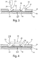
- FIG. 1 is a schematic view of an inlay 12 is shown.
- the FIG. 2 shows a schematic sectional view taken along the line II in FIG FIG. 1 ,
- This inlay 12 comprises at least one carrier film 14, on which an antenna 16 is applied.
- This antenna 16 in FIG. 1 is simplified in FIG. 2 shown as a layer.
- This antenna 16 comprises a plurality of windings 17.
- the antenna 16 is preferably printed, in particular printed by means of a silver paste.
- a microchip 15 is provided for contacting the antenna 16. This microchip 15 is fixed by an adhesive 18 on the carrier 14 and contacted with the antenna 16.
Landscapes
- Engineering & Computer Science (AREA)
- Computer Hardware Design (AREA)
- Microelectronics & Electronic Packaging (AREA)
- Physics & Mathematics (AREA)
- General Physics & Mathematics (AREA)
- Theoretical Computer Science (AREA)
- Lining Or Joining Of Plastics Or The Like (AREA)
- Details Of Aerials (AREA)
- Credit Cards Or The Like (AREA)
Applications Claiming Priority (1)
| Application Number | Priority Date | Filing Date | Title |
|---|---|---|---|
| DE102017103411.0A DE102017103411A1 (de) | 2017-02-20 | 2017-02-20 | Verfahren zur Herstellung eines Inlays für einen Folienverbund eines Sicherheits- und/oder Wertdokumentes sowie Inlay |
Publications (2)
| Publication Number | Publication Date |
|---|---|
| EP3364344A1 true EP3364344A1 (fr) | 2018-08-22 |
| EP3364344B1 EP3364344B1 (fr) | 2021-11-03 |
Family
ID=61007484
Family Applications (1)
| Application Number | Title | Priority Date | Filing Date |
|---|---|---|---|
| EP18152006.5A Active EP3364344B1 (fr) | 2017-02-20 | 2018-01-17 | Procédé de fabrication d'une incrustation en profondeur pour un film composite d'un document de sécurité et/ou de valeur ainsi qu'incrustation en profondeur |
Country Status (2)
| Country | Link |
|---|---|
| EP (1) | EP3364344B1 (fr) |
| DE (1) | DE102017103411A1 (fr) |
Citations (5)
| Publication number | Priority date | Publication date | Assignee | Title |
|---|---|---|---|---|
| EP0071255A2 (fr) * | 1981-07-30 | 1983-02-09 | Siemens Aktiengesellschaft | Carte portative pour le traitement d'informations |
| US20090057414A1 (en) * | 2005-02-11 | 2009-03-05 | Smart Packaging Solutions (Sps) | Method of Producing a Contactless Microelectronic Device, Such as for an Electronic Passport |
| DE102011001722A1 (de) | 2011-04-01 | 2012-10-04 | Bundesdruckerei Gmbh | Halbzeug zur Herstellung eines Chipkartenmoduls, Verfahren zur Herstellung des Halbzeuges sowie Verfahren zur Herstellung einer Chipkarte |
| DE102012001346A1 (de) * | 2012-01-24 | 2013-07-25 | Giesecke & Devrient Gmbh | Verfahren zum Herstellen eines Datenträgers |
| WO2014095232A1 (fr) | 2012-12-20 | 2014-06-26 | Bundesdruckerei Gmbh | Procédé de fabrication d'une incrustation et incrustation pour un ensemble de feuilles pour un document de valeur ou de sécurité |
Family Cites Families (2)
| Publication number | Priority date | Publication date | Assignee | Title |
|---|---|---|---|---|
| US6607135B1 (en) * | 1997-06-23 | 2003-08-19 | Rohm Co., Ltd. | Module for IC card, IC card, and method for manufacturing module for IC card |
| US9358722B2 (en) * | 2012-09-18 | 2016-06-07 | Assa Abloy Ab | Method of protecting an electrical component in a laminate |
-
2017
- 2017-02-20 DE DE102017103411.0A patent/DE102017103411A1/de not_active Withdrawn
-
2018
- 2018-01-17 EP EP18152006.5A patent/EP3364344B1/fr active Active
Patent Citations (5)
| Publication number | Priority date | Publication date | Assignee | Title |
|---|---|---|---|---|
| EP0071255A2 (fr) * | 1981-07-30 | 1983-02-09 | Siemens Aktiengesellschaft | Carte portative pour le traitement d'informations |
| US20090057414A1 (en) * | 2005-02-11 | 2009-03-05 | Smart Packaging Solutions (Sps) | Method of Producing a Contactless Microelectronic Device, Such as for an Electronic Passport |
| DE102011001722A1 (de) | 2011-04-01 | 2012-10-04 | Bundesdruckerei Gmbh | Halbzeug zur Herstellung eines Chipkartenmoduls, Verfahren zur Herstellung des Halbzeuges sowie Verfahren zur Herstellung einer Chipkarte |
| DE102012001346A1 (de) * | 2012-01-24 | 2013-07-25 | Giesecke & Devrient Gmbh | Verfahren zum Herstellen eines Datenträgers |
| WO2014095232A1 (fr) | 2012-12-20 | 2014-06-26 | Bundesdruckerei Gmbh | Procédé de fabrication d'une incrustation et incrustation pour un ensemble de feuilles pour un document de valeur ou de sécurité |
Also Published As
| Publication number | Publication date |
|---|---|
| DE102017103411A1 (de) | 2018-08-23 |
| EP3364344B1 (fr) | 2021-11-03 |
Similar Documents
| Publication | Publication Date | Title |
|---|---|---|
| DE10338444B4 (de) | Transponderinlay für ein Dokument zur Personenidentifikation sowie Verfahren zu dessen Herstellung | |
| DE102012205768B4 (de) | Transponderlage und Verfahren zu deren Herstellung | |
| EP2715619B1 (fr) | Document de sécurité ou de valeur, et procédé de production | |
| EP2297677B1 (fr) | Support de données portatif et procédé de fabrication de ce support de données | |
| EP2981416B1 (fr) | Page de données pour un document en forme de livret, et procédé de production dudite page de données | |
| EP2936397B1 (fr) | Procédé de fabrication d'une incrustation et incrustation pour un ensemble de feuilles pour un document de valeur ou de sécurité | |
| EP2807613A1 (fr) | Procédé de production d'un support de données, permettant d'éviter des contraintes mécaniques entre une puce et le corps de support de données | |
| EP2644377B1 (fr) | Procédé de fabrication de cavités dans des documents de sécurité, en particulier des cartes à puce | |
| DE102004004469A1 (de) | Verfahren zur Herstellung eines Sicherheitslagenaufbaus sowie Sicherheitslagenaufbau und einen solchen enthaltende Identifikationsdokumente | |
| EP3364344B1 (fr) | Procédé de fabrication d'une incrustation en profondeur pour un film composite d'un document de sécurité et/ou de valeur ainsi qu'incrustation en profondeur | |
| EP2571666B1 (fr) | Procédé de fabrication d'un elément incrusté pour un document de valeur et/ou de sécurité | |
| DE102008022016A1 (de) | RFID-Inlays für elektronische Identifikationsdokumente und Herstellungsverfahren hierfür | |
| EP1436777B1 (fr) | Procede de production d'un support de donnees et support de donnees produit selon ce procede | |
| DE102012203276B4 (de) | Verfahren zum Herstellen einer mindestens ein elektronisches Bauelement aufweisenden Foliengruppe und Verfahren zur Herstellung eines Wert- und/oder Sicherheitsdokuments | |
| EP3297844B1 (fr) | Procédé de fabrication d'un livre, en particulier pour un document du type livre ainsi qu'un feuille intercalaire et un bloc de feuilles | |
| EP3927558B1 (fr) | Procédé de fabrication d'un document de valeur ou de sécurité ainsi que document de sécurité pourvu d'un hologramme de sécurité | |
| EP1817176B1 (fr) | Matiere de support et procede pour produire un document de valeur | |
| DE102019118444B4 (de) | Verfahren zum Herstellen einer Chipkarten-Schichtenstruktur, und Chipkarten-Schichtenstruktur | |
| EP4013622B1 (fr) | Document de valeur et/ou de sécurité et son procédé de fabrication | |
| EP4621641A1 (fr) | Fabrication d'un corps support pour un support de données portable | |
| DE102016014994A1 (de) | Inlay für ein elektronisches Identifikationsdokument | |
| EP2018997A2 (fr) | Plaque, en particulier plaque d'immatriculation pour véhicule automobile | |
| DE102012203260A1 (de) | Verfahren zum Herstellen einer elektrischen Leiterzugstruktur und Wert- und/oder Sicherheitsdokument mit einer Transpondereinheit | |
| EP2981936A1 (fr) | Produit de valeur ou de sécurité, procédé pour le fabriquer ainsi que système de transmission de données sans contact | |
| WO1997018075A1 (fr) | Stratifie de recouvrement pour cartes en matiere plastique |
Legal Events
| Date | Code | Title | Description |
|---|---|---|---|
| PUAI | Public reference made under article 153(3) epc to a published international application that has entered the european phase |
Free format text: ORIGINAL CODE: 0009012 |
|
| STAA | Information on the status of an ep patent application or granted ep patent |
Free format text: STATUS: THE APPLICATION HAS BEEN PUBLISHED |
|
| AK | Designated contracting states |
Kind code of ref document: A1 Designated state(s): AL AT BE BG CH CY CZ DE DK EE ES FI FR GB GR HR HU IE IS IT LI LT LU LV MC MK MT NL NO PL PT RO RS SE SI SK SM TR |
|
| AX | Request for extension of the european patent |
Extension state: BA ME |
|
| STAA | Information on the status of an ep patent application or granted ep patent |
Free format text: STATUS: REQUEST FOR EXAMINATION WAS MADE |
|
| 17P | Request for examination filed |
Effective date: 20190222 |
|
| RBV | Designated contracting states (corrected) |
Designated state(s): AL AT BE BG CH CY CZ DE DK EE ES FI FR GB GR HR HU IE IS IT LI LT LU LV MC MK MT NL NO PL PT RO RS SE SI SK SM TR |
|
| STAA | Information on the status of an ep patent application or granted ep patent |
Free format text: STATUS: EXAMINATION IS IN PROGRESS |
|
| 17Q | First examination report despatched |
Effective date: 20190930 |
|
| GRAP | Despatch of communication of intention to grant a patent |
Free format text: ORIGINAL CODE: EPIDOSNIGR1 |
|
| STAA | Information on the status of an ep patent application or granted ep patent |
Free format text: STATUS: GRANT OF PATENT IS INTENDED |
|
| INTG | Intention to grant announced |
Effective date: 20210430 |
|
| GRAJ | Information related to disapproval of communication of intention to grant by the applicant or resumption of examination proceedings by the epo deleted |
Free format text: ORIGINAL CODE: EPIDOSDIGR1 |
|
| STAA | Information on the status of an ep patent application or granted ep patent |
Free format text: STATUS: EXAMINATION IS IN PROGRESS |
|
| GRAP | Despatch of communication of intention to grant a patent |
Free format text: ORIGINAL CODE: EPIDOSNIGR1 |
|
| STAA | Information on the status of an ep patent application or granted ep patent |
Free format text: STATUS: GRANT OF PATENT IS INTENDED |
|
| GRAS | Grant fee paid |
Free format text: ORIGINAL CODE: EPIDOSNIGR3 |
|
| INTC | Intention to grant announced (deleted) | ||
| GRAA | (expected) grant |
Free format text: ORIGINAL CODE: 0009210 |
|
| STAA | Information on the status of an ep patent application or granted ep patent |
Free format text: STATUS: THE PATENT HAS BEEN GRANTED |
|
| INTG | Intention to grant announced |
Effective date: 20210923 |
|
| AK | Designated contracting states |
Kind code of ref document: B1 Designated state(s): AL AT BE BG CH CY CZ DE DK EE ES FI FR GB GR HR HU IE IS IT LI LT LU LV MC MK MT NL NO PL PT RO RS SE SI SK SM TR |
|
| REG | Reference to a national code |
Ref country code: GB Ref legal event code: FG4D Free format text: NOT ENGLISH |
|
| REG | Reference to a national code |
Ref country code: AT Ref legal event code: REF Ref document number: 1444638 Country of ref document: AT Kind code of ref document: T Effective date: 20211115 Ref country code: CH Ref legal event code: EP |
|
| REG | Reference to a national code |
Ref country code: IE Ref legal event code: FG4D Free format text: LANGUAGE OF EP DOCUMENT: GERMAN |
|
| REG | Reference to a national code |
Ref country code: DE Ref legal event code: R096 Ref document number: 502018007639 Country of ref document: DE |
|
| REG | Reference to a national code |
Ref country code: LT Ref legal event code: MG9D |
|
| REG | Reference to a national code |
Ref country code: NL Ref legal event code: MP Effective date: 20211103 |
|
| PG25 | Lapsed in a contracting state [announced via postgrant information from national office to epo] |
Ref country code: RS Free format text: LAPSE BECAUSE OF FAILURE TO SUBMIT A TRANSLATION OF THE DESCRIPTION OR TO PAY THE FEE WITHIN THE PRESCRIBED TIME-LIMIT Effective date: 20211103 Ref country code: LT Free format text: LAPSE BECAUSE OF FAILURE TO SUBMIT A TRANSLATION OF THE DESCRIPTION OR TO PAY THE FEE WITHIN THE PRESCRIBED TIME-LIMIT Effective date: 20211103 Ref country code: FI Free format text: LAPSE BECAUSE OF FAILURE TO SUBMIT A TRANSLATION OF THE DESCRIPTION OR TO PAY THE FEE WITHIN THE PRESCRIBED TIME-LIMIT Effective date: 20211103 Ref country code: BG Free format text: LAPSE BECAUSE OF FAILURE TO SUBMIT A TRANSLATION OF THE DESCRIPTION OR TO PAY THE FEE WITHIN THE PRESCRIBED TIME-LIMIT Effective date: 20220203 |
|
| PG25 | Lapsed in a contracting state [announced via postgrant information from national office to epo] |
Ref country code: IS Free format text: LAPSE BECAUSE OF FAILURE TO SUBMIT A TRANSLATION OF THE DESCRIPTION OR TO PAY THE FEE WITHIN THE PRESCRIBED TIME-LIMIT Effective date: 20220303 Ref country code: SE Free format text: LAPSE BECAUSE OF FAILURE TO SUBMIT A TRANSLATION OF THE DESCRIPTION OR TO PAY THE FEE WITHIN THE PRESCRIBED TIME-LIMIT Effective date: 20211103 Ref country code: PT Free format text: LAPSE BECAUSE OF FAILURE TO SUBMIT A TRANSLATION OF THE DESCRIPTION OR TO PAY THE FEE WITHIN THE PRESCRIBED TIME-LIMIT Effective date: 20220303 Ref country code: PL Free format text: LAPSE BECAUSE OF FAILURE TO SUBMIT A TRANSLATION OF THE DESCRIPTION OR TO PAY THE FEE WITHIN THE PRESCRIBED TIME-LIMIT Effective date: 20211103 Ref country code: NO Free format text: LAPSE BECAUSE OF FAILURE TO SUBMIT A TRANSLATION OF THE DESCRIPTION OR TO PAY THE FEE WITHIN THE PRESCRIBED TIME-LIMIT Effective date: 20220203 Ref country code: NL Free format text: LAPSE BECAUSE OF FAILURE TO SUBMIT A TRANSLATION OF THE DESCRIPTION OR TO PAY THE FEE WITHIN THE PRESCRIBED TIME-LIMIT Effective date: 20211103 Ref country code: LV Free format text: LAPSE BECAUSE OF FAILURE TO SUBMIT A TRANSLATION OF THE DESCRIPTION OR TO PAY THE FEE WITHIN THE PRESCRIBED TIME-LIMIT Effective date: 20211103 Ref country code: HR Free format text: LAPSE BECAUSE OF FAILURE TO SUBMIT A TRANSLATION OF THE DESCRIPTION OR TO PAY THE FEE WITHIN THE PRESCRIBED TIME-LIMIT Effective date: 20211103 Ref country code: GR Free format text: LAPSE BECAUSE OF FAILURE TO SUBMIT A TRANSLATION OF THE DESCRIPTION OR TO PAY THE FEE WITHIN THE PRESCRIBED TIME-LIMIT Effective date: 20220204 Ref country code: ES Free format text: LAPSE BECAUSE OF FAILURE TO SUBMIT A TRANSLATION OF THE DESCRIPTION OR TO PAY THE FEE WITHIN THE PRESCRIBED TIME-LIMIT Effective date: 20211103 |
|
| PG25 | Lapsed in a contracting state [announced via postgrant information from national office to epo] |
Ref country code: SM Free format text: LAPSE BECAUSE OF FAILURE TO SUBMIT A TRANSLATION OF THE DESCRIPTION OR TO PAY THE FEE WITHIN THE PRESCRIBED TIME-LIMIT Effective date: 20211103 Ref country code: SK Free format text: LAPSE BECAUSE OF FAILURE TO SUBMIT A TRANSLATION OF THE DESCRIPTION OR TO PAY THE FEE WITHIN THE PRESCRIBED TIME-LIMIT Effective date: 20211103 Ref country code: RO Free format text: LAPSE BECAUSE OF FAILURE TO SUBMIT A TRANSLATION OF THE DESCRIPTION OR TO PAY THE FEE WITHIN THE PRESCRIBED TIME-LIMIT Effective date: 20211103 Ref country code: EE Free format text: LAPSE BECAUSE OF FAILURE TO SUBMIT A TRANSLATION OF THE DESCRIPTION OR TO PAY THE FEE WITHIN THE PRESCRIBED TIME-LIMIT Effective date: 20211103 Ref country code: DK Free format text: LAPSE BECAUSE OF FAILURE TO SUBMIT A TRANSLATION OF THE DESCRIPTION OR TO PAY THE FEE WITHIN THE PRESCRIBED TIME-LIMIT Effective date: 20211103 Ref country code: CZ Free format text: LAPSE BECAUSE OF FAILURE TO SUBMIT A TRANSLATION OF THE DESCRIPTION OR TO PAY THE FEE WITHIN THE PRESCRIBED TIME-LIMIT Effective date: 20211103 |
|
| REG | Reference to a national code |
Ref country code: DE Ref legal event code: R097 Ref document number: 502018007639 Country of ref document: DE |
|
| PG25 | Lapsed in a contracting state [announced via postgrant information from national office to epo] |
Ref country code: MC Free format text: LAPSE BECAUSE OF FAILURE TO SUBMIT A TRANSLATION OF THE DESCRIPTION OR TO PAY THE FEE WITHIN THE PRESCRIBED TIME-LIMIT Effective date: 20211103 |
|
| REG | Reference to a national code |
Ref country code: CH Ref legal event code: PL |
|
| PLBE | No opposition filed within time limit |
Free format text: ORIGINAL CODE: 0009261 |
|
| STAA | Information on the status of an ep patent application or granted ep patent |
Free format text: STATUS: NO OPPOSITION FILED WITHIN TIME LIMIT |
|
| REG | Reference to a national code |
Ref country code: BE Ref legal event code: MM Effective date: 20220131 |
|
| 26N | No opposition filed |
Effective date: 20220804 |
|
| PG25 | Lapsed in a contracting state [announced via postgrant information from national office to epo] |
Ref country code: LU Free format text: LAPSE BECAUSE OF NON-PAYMENT OF DUE FEES Effective date: 20220117 Ref country code: AL Free format text: LAPSE BECAUSE OF FAILURE TO SUBMIT A TRANSLATION OF THE DESCRIPTION OR TO PAY THE FEE WITHIN THE PRESCRIBED TIME-LIMIT Effective date: 20211103 |
|
| PG25 | Lapsed in a contracting state [announced via postgrant information from national office to epo] |
Ref country code: SI Free format text: LAPSE BECAUSE OF FAILURE TO SUBMIT A TRANSLATION OF THE DESCRIPTION OR TO PAY THE FEE WITHIN THE PRESCRIBED TIME-LIMIT Effective date: 20211103 Ref country code: BE Free format text: LAPSE BECAUSE OF NON-PAYMENT OF DUE FEES Effective date: 20220131 |
|
| PG25 | Lapsed in a contracting state [announced via postgrant information from national office to epo] |
Ref country code: LI Free format text: LAPSE BECAUSE OF NON-PAYMENT OF DUE FEES Effective date: 20220131 Ref country code: CH Free format text: LAPSE BECAUSE OF NON-PAYMENT OF DUE FEES Effective date: 20220131 |
|
| PG25 | Lapsed in a contracting state [announced via postgrant information from national office to epo] |
Ref country code: IE Free format text: LAPSE BECAUSE OF NON-PAYMENT OF DUE FEES Effective date: 20220117 |
|
| PG25 | Lapsed in a contracting state [announced via postgrant information from national office to epo] |
Ref country code: IT Free format text: LAPSE BECAUSE OF FAILURE TO SUBMIT A TRANSLATION OF THE DESCRIPTION OR TO PAY THE FEE WITHIN THE PRESCRIBED TIME-LIMIT Effective date: 20211103 |
|
| P01 | Opt-out of the competence of the unified patent court (upc) registered |
Effective date: 20230526 |
|
| REG | Reference to a national code |
Ref country code: AT Ref legal event code: MM01 Ref document number: 1444638 Country of ref document: AT Kind code of ref document: T Effective date: 20230117 |
|
| PG25 | Lapsed in a contracting state [announced via postgrant information from national office to epo] |
Ref country code: HU Free format text: LAPSE BECAUSE OF FAILURE TO SUBMIT A TRANSLATION OF THE DESCRIPTION OR TO PAY THE FEE WITHIN THE PRESCRIBED TIME-LIMIT; INVALID AB INITIO Effective date: 20180117 |
|
| PG25 | Lapsed in a contracting state [announced via postgrant information from national office to epo] |
Ref country code: AT Free format text: LAPSE BECAUSE OF NON-PAYMENT OF DUE FEES Effective date: 20230117 |
|
| PG25 | Lapsed in a contracting state [announced via postgrant information from national office to epo] |
Ref country code: MK Free format text: LAPSE BECAUSE OF FAILURE TO SUBMIT A TRANSLATION OF THE DESCRIPTION OR TO PAY THE FEE WITHIN THE PRESCRIBED TIME-LIMIT Effective date: 20211103 Ref country code: CY Free format text: LAPSE BECAUSE OF FAILURE TO SUBMIT A TRANSLATION OF THE DESCRIPTION OR TO PAY THE FEE WITHIN THE PRESCRIBED TIME-LIMIT Effective date: 20211103 Ref country code: AT Free format text: LAPSE BECAUSE OF NON-PAYMENT OF DUE FEES Effective date: 20230117 |
|
| PG25 | Lapsed in a contracting state [announced via postgrant information from national office to epo] |
Ref country code: MT Free format text: LAPSE BECAUSE OF FAILURE TO SUBMIT A TRANSLATION OF THE DESCRIPTION OR TO PAY THE FEE WITHIN THE PRESCRIBED TIME-LIMIT Effective date: 20211103 |
|
| PG25 | Lapsed in a contracting state [announced via postgrant information from national office to epo] |
Ref country code: TR Free format text: LAPSE BECAUSE OF FAILURE TO SUBMIT A TRANSLATION OF THE DESCRIPTION OR TO PAY THE FEE WITHIN THE PRESCRIBED TIME-LIMIT Effective date: 20211103 |
|
| PGFP | Annual fee paid to national office [announced via postgrant information from national office to epo] |
Ref country code: GB Payment date: 20260122 Year of fee payment: 9 |
|
| PGFP | Annual fee paid to national office [announced via postgrant information from national office to epo] |
Ref country code: DE Payment date: 20260120 Year of fee payment: 9 |
|
| PGFP | Annual fee paid to national office [announced via postgrant information from national office to epo] |
Ref country code: AT Payment date: 20260410 Year of fee payment: 5 |
|
| PGFP | Annual fee paid to national office [announced via postgrant information from national office to epo] |
Ref country code: FR Payment date: 20260128 Year of fee payment: 9 |