EP3364400B1 - Randlose anzeigevorrichtung und verfahren zur herstellung davon - Google Patents
Randlose anzeigevorrichtung und verfahren zur herstellung davon Download PDFInfo
- Publication number
- EP3364400B1 EP3364400B1 EP16874734.3A EP16874734A EP3364400B1 EP 3364400 B1 EP3364400 B1 EP 3364400B1 EP 16874734 A EP16874734 A EP 16874734A EP 3364400 B1 EP3364400 B1 EP 3364400B1
- Authority
- EP
- European Patent Office
- Prior art keywords
- display region
- display device
- display
- rimless
- circuit board
- Prior art date
- Legal status (The legal status is an assumption and is not a legal conclusion. Google has not performed a legal analysis and makes no representation as to the accuracy of the status listed.)
- Active
Links
Images
Classifications
-
- G—PHYSICS
- G06—COMPUTING OR CALCULATING; COUNTING
- G06F—ELECTRIC DIGITAL DATA PROCESSING
- G06F1/00—Details not covered by groups G06F3/00 - G06F13/00 and G06F21/00
- G06F1/16—Constructional details or arrangements
- G06F1/1613—Constructional details or arrangements for portable computers
- G06F1/1633—Constructional details or arrangements of portable computers not specific to the type of enclosures covered by groups G06F1/1615 - G06F1/1626
- G06F1/1637—Details related to the display arrangement, including those related to the mounting of the display in the housing
- G06F1/1652—Details related to the display arrangement, including those related to the mounting of the display in the housing the display being flexible, e.g. mimicking a sheet of paper, or rollable
-
- G—PHYSICS
- G06—COMPUTING OR CALCULATING; COUNTING
- G06F—ELECTRIC DIGITAL DATA PROCESSING
- G06F1/00—Details not covered by groups G06F3/00 - G06F13/00 and G06F21/00
- G06F1/16—Constructional details or arrangements
- G06F1/1613—Constructional details or arrangements for portable computers
- G06F1/1633—Constructional details or arrangements of portable computers not specific to the type of enclosures covered by groups G06F1/1615 - G06F1/1626
- G06F1/1637—Details related to the display arrangement, including those related to the mounting of the display in the housing
-
- G—PHYSICS
- G09—EDUCATION; CRYPTOGRAPHY; DISPLAY; ADVERTISING; SEALS
- G09F—DISPLAYING; ADVERTISING; SIGNS; LABELS OR NAME-PLATES; SEALS
- G09F9/00—Indicating arrangements for variable information in which the information is built-up on a support by selection or combination of individual elements
- G09F9/30—Indicating arrangements for variable information in which the information is built-up on a support by selection or combination of individual elements in which the desired character or characters are formed by combining individual elements
- G09F9/301—Indicating arrangements for variable information in which the information is built-up on a support by selection or combination of individual elements in which the desired character or characters are formed by combining individual elements flexible foldable or roll-able electronic displays, e.g. thin LCD, OLED
-
- G—PHYSICS
- G09—EDUCATION; CRYPTOGRAPHY; DISPLAY; ADVERTISING; SEALS
- G09F—DISPLAYING; ADVERTISING; SIGNS; LABELS OR NAME-PLATES; SEALS
- G09F9/00—Indicating arrangements for variable information in which the information is built-up on a support by selection or combination of individual elements
- G09F9/30—Indicating arrangements for variable information in which the information is built-up on a support by selection or combination of individual elements in which the desired character or characters are formed by combining individual elements
- G09F9/33—Indicating arrangements for variable information in which the information is built-up on a support by selection or combination of individual elements in which the desired character or characters are formed by combining individual elements being semiconductor devices, e.g. diodes
- G09F9/335—Indicating arrangements for variable information in which the information is built-up on a support by selection or combination of individual elements in which the desired character or characters are formed by combining individual elements being semiconductor devices, e.g. diodes being organic light emitting diodes [OLED]
-
- H—ELECTRICITY
- H05—ELECTRIC TECHNIQUES NOT OTHERWISE PROVIDED FOR
- H05K—PRINTED CIRCUITS; CASINGS OR CONSTRUCTIONAL DETAILS OF ELECTRIC APPARATUS; MANUFACTURE OF ASSEMBLAGES OF ELECTRICAL COMPONENTS
- H05K1/00—Printed circuits
- H05K1/02—Details
- H05K1/0277—Bendability or stretchability details
- H05K1/028—Bending or folding regions of flexible printed circuits
-
- H—ELECTRICITY
- H05—ELECTRIC TECHNIQUES NOT OTHERWISE PROVIDED FOR
- H05K—PRINTED CIRCUITS; CASINGS OR CONSTRUCTIONAL DETAILS OF ELECTRIC APPARATUS; MANUFACTURE OF ASSEMBLAGES OF ELECTRICAL COMPONENTS
- H05K1/00—Printed circuits
- H05K1/18—Printed circuits structurally associated with non-printed electric components
- H05K1/189—Printed circuits structurally associated with non-printed electric components characterised by the use of flexible or folded printed circuits
-
- H—ELECTRICITY
- H10—SEMICONDUCTOR DEVICES; ELECTRIC SOLID-STATE DEVICES NOT OTHERWISE PROVIDED FOR
- H10K—ORGANIC ELECTRIC SOLID-STATE DEVICES
- H10K59/00—Integrated devices, or assemblies of multiple devices, comprising at least one organic light-emitting element covered by group H10K50/00
- H10K59/10—OLED displays
-
- H—ELECTRICITY
- H10—SEMICONDUCTOR DEVICES; ELECTRIC SOLID-STATE DEVICES NOT OTHERWISE PROVIDED FOR
- H10K—ORGANIC ELECTRIC SOLID-STATE DEVICES
- H10K77/00—Constructional details of devices covered by this subclass and not covered by groups H10K10/80, H10K30/80, H10K50/80 or H10K59/80
- H10K77/10—Substrates, e.g. flexible substrates
- H10K77/111—Flexible substrates
-
- H—ELECTRICITY
- H05—ELECTRIC TECHNIQUES NOT OTHERWISE PROVIDED FOR
- H05K—PRINTED CIRCUITS; CASINGS OR CONSTRUCTIONAL DETAILS OF ELECTRIC APPARATUS; MANUFACTURE OF ASSEMBLAGES OF ELECTRICAL COMPONENTS
- H05K2201/00—Indexing scheme relating to printed circuits covered by H05K1/00
- H05K2201/10—Details of components or other objects attached to or integrated in a printed circuit board
- H05K2201/10007—Types of components
- H05K2201/10106—Light emitting diode [LED]
-
- H—ELECTRICITY
- H05—ELECTRIC TECHNIQUES NOT OTHERWISE PROVIDED FOR
- H05K—PRINTED CIRCUITS; CASINGS OR CONSTRUCTIONAL DETAILS OF ELECTRIC APPARATUS; MANUFACTURE OF ASSEMBLAGES OF ELECTRICAL COMPONENTS
- H05K2201/00—Indexing scheme relating to printed circuits covered by H05K1/00
- H05K2201/10—Details of components or other objects attached to or integrated in a printed circuit board
- H05K2201/10007—Types of components
- H05K2201/10128—Display
-
- H—ELECTRICITY
- H10—SEMICONDUCTOR DEVICES; ELECTRIC SOLID-STATE DEVICES NOT OTHERWISE PROVIDED FOR
- H10K—ORGANIC ELECTRIC SOLID-STATE DEVICES
- H10K2102/00—Constructional details relating to the organic devices covered by this subclass
- H10K2102/301—Details of OLEDs
-
- H—ELECTRICITY
- H10—SEMICONDUCTOR DEVICES; ELECTRIC SOLID-STATE DEVICES NOT OTHERWISE PROVIDED FOR
- H10K—ORGANIC ELECTRIC SOLID-STATE DEVICES
- H10K2102/00—Constructional details relating to the organic devices covered by this subclass
- H10K2102/301—Details of OLEDs
- H10K2102/302—Details of OLEDs of OLED structures
- H10K2102/3023—Direction of light emission
-
- H—ELECTRICITY
- H10—SEMICONDUCTOR DEVICES; ELECTRIC SOLID-STATE DEVICES NOT OTHERWISE PROVIDED FOR
- H10K—ORGANIC ELECTRIC SOLID-STATE DEVICES
- H10K2102/00—Constructional details relating to the organic devices covered by this subclass
- H10K2102/301—Details of OLEDs
- H10K2102/311—Flexible OLED
-
- Y—GENERAL TAGGING OF NEW TECHNOLOGICAL DEVELOPMENTS; GENERAL TAGGING OF CROSS-SECTIONAL TECHNOLOGIES SPANNING OVER SEVERAL SECTIONS OF THE IPC; TECHNICAL SUBJECTS COVERED BY FORMER USPC CROSS-REFERENCE ART COLLECTIONS [XRACs] AND DIGESTS
- Y02—TECHNOLOGIES OR APPLICATIONS FOR MITIGATION OR ADAPTATION AGAINST CLIMATE CHANGE
- Y02E—REDUCTION OF GREENHOUSE GAS [GHG] EMISSIONS, RELATED TO ENERGY GENERATION, TRANSMISSION OR DISTRIBUTION
- Y02E10/00—Energy generation through renewable energy sources
- Y02E10/50—Photovoltaic [PV] energy
- Y02E10/549—Organic PV cells
Definitions
- the present invention relates to the field of flat panel display technology, and in particular relates to a rimless display device and a preparation method thereof.
- OLED Organic Light-Emitting Diode
- OLED Organic Light-Emitting Diode
- advantages such as high brightness of light-emitting, color richness, low-voltage direct-current driving, simple preparation process.
- OLED has broader field of vision and thus can be made into products with larger sizes to meet users' requirements for various dimensions. It is determined by the aforementioned significant advantages that OLED will become the next-generation mainstream display technology.
- the existing display screens on the market comprise a display area and a rim, but in order to make OLED display devices look compact and fashionable, OLED provided with a narrow rim has become a trend of OLED display device development.
- OLED display panels in prior art because a side portion of the array layer is required for electrical circuit cabling, the so-called “rimless” therein is just making the portion reserved for IC or periphery circuits as smaller as possible, which can only be regarded as an ultra-narrow rim or ultra-narrow rim display device, not a real rimless display device.
- CN201110414415 discloses a display device, its periphery circuits and part of its cabling are folded into an arc structure, and a foldable substrate is folded at a middle portion of the cabling part, so as to form a display screen with a narrow rim.
- US 2014/002385 A1 discloses a flexible display panel and a display apparatus including the flexible display panel are disclosed.
- the flexible display panel includes an encapsulated panel, a first protective film on one side of the encapsulated panel, and a second protective film on another side of the encapsulated panel.
- the encapsulated panel includes a flexible panel and a flexible encapsulation member on the flexible panel.
- the flexible panel includes a first region on a first plane and that includes a display region, and a second region on a second plane that is bent with respect to the first plane and that includes a non-display region.
- the flexible encapsulation member encapsulates the display region.
- the display apparatus also includes a support unit for maintaining a shape of the flexible panel.
- a technical problem to be solved by the present invention is that a side portion of the array layer of OLED display panels in prior art is required for electrical circuit cabling and therefore a rimless display device cannot be manufactured.
- the present invention provides a rimless display device that can achieve a real rimless display screen body, thereby further increasing the screen proportion and greatly improving the view effect.
- the present invention provides a rimless display according to claim 1.
- the non-display region is fixed on a lateral surface or a rear surface of the display device after the non-display region is folded along a boundary between the display region and the non-display region.
- the parts of the non-display region on two neighboring sides of the display region have a disconnected structure.
- the rimless display device further comprises a drive circuit board assembly arranged on a side of the rigid base plate away from the organic light-emitting layer, wherein, the drive circuit board assembly and the display region have overlapping projections on the flexible substrate.
- the non-display region is fixed on a rear surface of the drive circuit board assembly after the non-display region is folded; when the rimless display device is a bottom-emitting display device, the non-display region is fixed on a lateral surface of the drive circuit board assembly after the non-display region is folded.
- the step S3 comprises: making a part of the non-display region where the GIP is located into a hollowed-out structure, removing the part of the rigid base plate at a location corresponding to the non-display region, and fixing the non-display region on a lateral surface of the drive circuit board assembly after folding the non-display region.
- the step S3 comprises: making a part of the non-display region where the GIP is located into a hollowed-out structure, removing the part of the rigid base plate at a location corresponding to the non-display region, and fixing the non-display region on a rear surface of the drive circuit board assembly after folding the non-display region.
- the above-mentioned technical scheme of the present invention has the following advantages:
- a part of the rigid base plate at a location corresponding to the non-display region is removed, and then the non-display region of the flexible substrate is fixed on a lateral surface or a rear surface of the display device after being folded. Because the flexible substrate is directly folded, a real rimless display screen body can be achieved, thereby further increasing the screen proportion and greatly improving the view effect.
- the non-display region is manufactured to have a hollowed-out structure, only the part of the flexible substrate in a zone adjacent to the cabling remains in this hollowed-out structure.
- This hollowed-out structure can effectively release bending stress and can be bended by 90° without damaging the cabling.
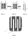
- the reference numerals in the Drawings represent: 1-rigid base plate, 2-display region, 3-non-display region, 4-drive circuit board assembly, 5-cabling, 6-hollowed-out structure.
- a rimless display device of the present invention comprises a flexible substrate formed on a rigid base plate 1, the flexible substrate is provided with a display region 2 and a non-display region 3; an anode layer, an organic light-emitting layer and a cathode layer are arranged in the display region 2; wherein, after a part of the rigid base plate 1 at a location corresponding to the non-display region 3 is removed, the non-display region 3 of the flexible substrate is fixed on a lateral surface or a rear surface of the display device after being folded.
- the organic light-emitting layer comprises a hole injection layer and/or a hole transport layer, a light-emitting layer, an electron transport layer and/or an electron injection layer.
- the non-display region 3 is fixed on a lateral surface or a rear surface of the display device after being folded along a boundary between the display region 2 and the non-display region 3.
- the non-display region 3 has a hollowed-out structure 6 as shown in Figure 2 , wherein only the part of the flexible substrate in a zone adjacent to the cabling 5 remains in this hollowed-out structure 6.
- GIP gate driving circuit
- the parts of the non-display region 3 on two neighboring sides of the display region 2 have a disconnected structure. Specifically, as shown in Figure 1-2 , the part of the non-display region where the gate driving circuit (GIP) is located is disconnected from the part of the non-display region where the Integrated Circuit (abbreviated as IC) is located. Such a disconnected structure allows the part of the non-display region where the gate driving circuit (GIP) is located and the part of the non-display region where the Integrated Circuit (IC) is located to be individually fixed on a lateral surface or a rear surface of the display device after being respectively folded along the boundary.
- GIP gate driving circuit
- the rimless display device of the present invention further comprises a drive circuit board assembly 4 arranged on a side of the rigid base plate away from the organic light-emitting layer, wherein the drive circuit board assembly 4 and the display region 2 have overlapping projections on the flexible substrate.
- the non-display region 3 is fixed on a rear surface of the drive circuit board assembly 4 after being folded.
- the rear surface of the drive circuit board assembly 4 herein refers to the inside surface of the drive circuit board assembly 4 facing the rigid base plate. Because it is a top-emitting display device, fixing the folded non-display region 3 on the rear surface of the drive circuit board assembly 4 would not cause obstruction to the light emitted from the display region 2.
- the non-display region 3 is fixed on a lateral surface of the drive circuit board assembly 4 after being folded.
- the lateral surface of the drive circuit board assembly 4 herein refers to a periphery surface of the drive circuit board assembly 4 outside the projection range of the display region 2.
- a preparation method of the rimless display device which comprises the following steps:
- the step S3 comprises: making a part of the non-display region where the GIP is located into a hollowed-out structure 6, removing the part of the rigid base plate at a location corresponding to the non-display region 3, and fixing the non-display region 3 on a lateral surface of the drive circuit board assembly 4 after folding the non-display region 3.
- fixing the folded non-display region 3 on a periphery surface of the drive circuit board assembly 4 outside the projection range of the display region 2, with the drive circuit board assembly 4 itself being transparent can avoid causing obstruction to the light emitted from the display region 2.
- the step S3 comprises: making a part of the non-display region where the GIP is located into a hollowed-out structure 6, removing the part of the rigid base plate at a location corresponding to the non-display region 3, and fixing the non-display region 3 on a rear surface of the drive circuit board assembly 4 after folding the non-display region 3.
- fixing the folded non-display region 3 on the rear surface of the drive circuit board assembly 4 would not cause obstruction to the light emitted from the display region 2.
- a part of the rigid base plate at a location corresponding to the non-display region is removed, and then the non-display region of the flexible substrate is fixed on a lateral surface or a rear surface of the display device after being folded. Because the flexible substrate is directly folded, a real rimless display screen body can be achieved, thereby further increasing the screen proportion and greatly improving the view effect.
- the anode layer can adopt an inorganic material or an organic conducting polymer.
- the inorganic material is usually a metal oxide such as indium tin oxide (ITO), zinc oxide (ZnO), indium zinc oxide (IZO), or a metal with high work function such as gold, copper, silver, preferably, it is ITO.
- the organic conducting polymer is preferably selected from Polythiophene / Polyethylene based sodium benzene sulfonate (hereinafter abbreviated as PEDOT:PSS) and Polyaniline (hereinafter abbreviated as PANI).
- the cathode layer usually adopts metal with low work function such as silver, lithium, magnesium, calcium, strontium, aluminum, indium; or their alloy with copper, gold, silver; or an electrode layer formed by alternately arranged metal and metal fluoride.
- the cathode layer is preferably an AI layer.
- the material of the hole transport layer may adopt a low molecular material selected from the aryl-amine type, the carbazole type or the branched polymer species, preferably NPB and TCTA.
- the material of the hole injection layer may adopt HAT-CN (2,3,6,7,10,11-hexacyano-1,4,5,8,9,12-hexa-aza-benzene) doped with F4TCNQ, or may adopt copper peptide cyanine (CuPc), or may adopt a metal oxide such as molybdenum oxide, rhenium oxide.
- the light-emitting material in the light-emitting layer may adopt a fluorescent dye selected from the coumarin type such as DMQA or C545T, the bis-pyran type such as DCJTB or DCM; or may contain a metal complex of Ir, Pt, Os, Ru, Rh, Pd, lanthanides or actinides.
- the host material in the light-emitting layer may be selected from an ordinary matrix material, such as 4,4'-di-(carbazole-9-yl)-biphenyl (CBP).
- an ordinary matrix material such as 4,4'-di-(carbazole-9-yl)-biphenyl (CBP).
- the material of the electron transport layer of the present invention may be selected from an ordinary electron transport layer material, such as aromatic condensed ring compounds (e.g., Pentacene, Perylene) or o-phenanthrolines (e.g., Bphen, BCP).
- aromatic condensed ring compounds e.g., Pentacene, Perylene
- o-phenanthrolines e.g., Bphen, BCP
- the flexible substrate may adopt polyester, polyimide compound material, or may be a thin metal sheet.
- the laminating and encapsulation thereof may adopt any suitable method know to a person skilled in the art.
Landscapes
- Engineering & Computer Science (AREA)
- Theoretical Computer Science (AREA)
- Computer Hardware Design (AREA)
- Physics & Mathematics (AREA)
- General Physics & Mathematics (AREA)
- Human Computer Interaction (AREA)
- General Engineering & Computer Science (AREA)
- Microelectronics & Electronic Packaging (AREA)
- Optics & Photonics (AREA)
- Electroluminescent Light Sources (AREA)
- Devices For Indicating Variable Information By Combining Individual Elements (AREA)
Claims (8)
- Randlose Anzeigevorrichtung, umfassend
eine steife Grundplatte (1),
ein auf der steifen Grundplatte (1) vorgesehenes flexibles Substrat, das mit einem Anzeigebereich (2), auf dem eine organische lichtemittierende Schicht angeordnet ist, und einem Nichtanzeigebereich (3) versehen ist,
wobei der Nichtanzeigebereich (3) des flexiblen Substrats auf einer Seitenfläche oder Rückseite der Anzeigevorrichtung befestigt wird, nachdem ein Teil der steifen Grundplatte (1) an einer Stelle, die dem Nichtanzeigebereich (3) entspricht, abgenommen wird und der Nichtanzeigebereich gefaltet wird, wobei der Nichtanzeigebereich (3) mit einem IC-Bereich (integrierten Schaltkreisbereich) und einem Gate-Driver-Schaltungsbereich ("GIP-Bereich") versehen ist und der GIP-Bereich eine hohle Struktur aufweist. - Randlose Anzeigevorrichtung nach Anspruch 1, dadurch gekennzeichnet, dass der Nichtanzeigeberiech (3) auf einer Seitenfläche oder Rückseite der Anzeigevorrichtung befestigt wird, nachdem der Nichtanzeigebereich entlang einer Grenze zwischen Anzeigebereich (2) und Nichtanzeigebereich (3) gefaltet wird.
- Randlose Anzeigevorrichtung nach Anspruch 1, dadurch gekennzeichnet, dass die Teile des Nichtanzeigebereichs (3) auf zwei benachbarten Seiten des Anzeigebereichs (2) eine getrennte Struktur aufweisen.
- Randlose Anzeigevorrichtung nach Anspruch 3, dadurch gekennzeichnet, dass sie ferner eine Antriebskreisplatteneinrichtung (4) umfasst, die auf einer Seite der steifen Grundplatte (1) fern der organischen lichtemittierenden Schicht angeordnet ist, wobei die Antriebskreisplatteneinrichtung (4) und der Anzeigebereich (2) sich überschneidende Vorsprünge auf dem flexiblen Substrat aufweisen.
- Randlose Anzeigevorrichtung nach Anspruch 4, dadurch gekennzeichnet, dass, wenn es sich bei der randlosen Anzeigevorrichtung um eine oberflächenemittierende Anzeigevorrichtung handelt, der Nichtanzeigebereich (3) auf einer Rückseite der Antriebskreisplatteneinrichtung (4) befestigt wird, nachdem der Nichtanzeigebereich gefaltet wird; wenn es sich bei der randlosen Anzeigevorrichtung um eine unterseitenemittierende Anzeigevorrichtung handelt, der Nichtanzeigebereich (3) auf einer Seitenfläche der Antriebskreisplatteneinrichtung (4) befestigt wird, nachdem der Nichtanzeigebereich gefaltet wird.
- Verfahren zum Herstellen einer randlosen Anzeigevorrichtung, dadurch gekennzeichnet, dass es folgende Schritte umfasst:S1, Vorsehen eines flexiblen Substrats auf einer steifen Grundplatte (1), Teilen des flexiblen Substrats in einen Anzeigebereich (2) und einen Nichtanzeigebereich (3) und Vorsehen einer Antriebskreisplatteneinrichtung (4) auf einer Seite der steifen Grundplatte (1) fern dem flexiblen Substrat.S2, Anfertigen einer organischen lichtemittierenden Schicht im Anzeigebereich (2), Anfertigen von IC und GIP im Nichtanzeigebereich (3) und Ausbilden eines Teils des Nichtanzeigebereichs (3), in dem die GIP angeordnet ist, als hohle Struktur,S3, Abnehmen eines Teils der steifen Grundplatte (1) an einer Stelle, die dem Nichtanzeigebereich (3) entspricht, und Befestigen des Nichtanzeigebereichs (3) auf einer Seitenfläche oder Rückseite der Antriebskreisplatteneinrichtung (4) nach dem Falten des Nichtanzeigebereichs (3).
- Verfahren zum Herstellen einer randlosen Anzeigevorrichtung nach Anspruch 6, dadurch gekennzeichnet, dass, wenn es sich bei der Anzeigevorrichtung um eine unterseitenemittierende Anzeigevorrichtung handelt, der Schritt S3 umfasst:
Abnehmen des Teils der steifen Grundplatte (1) an einer Stelle, die dem Nichtanzeigebereich (3) entspricht, und Befestigen des Nichtanzeigebereichs (3) auf einer Seitenfläche der Antriebskreisplatteneinrichtung (4) nach dem Falten des Nichtanzeigebereichs (3). - Verfahren zum Herstellen einer randlosen Anzeigevorrichtung nach Anspruch 6, dadurch gekennzeichnet, dass, wenn es sich bei der Anzeigevorrichtung um eine oberflächenemittierende Anzeigevorrichtung handelt, der Schritt S3 umfasst:
Abnehmen des Teils der steifen Grundplatte an einer Stelle, die dem Nichtanzeigebereich (3) entspricht, und Befestigen des Nichtanzeigebereichs (3) auf einer Rückseite der Antriebskreisplatteneinrichtung (4) nach dem Falten des Nichtanzeigebereichs (3).
Applications Claiming Priority (2)
| Application Number | Priority Date | Filing Date | Title |
|---|---|---|---|
| CN201510945235.2A CN106887187A (zh) | 2015-12-16 | 2015-12-16 | 一种无边框显示装置及其制备方法 |
| PCT/CN2016/107983 WO2017101677A1 (zh) | 2015-12-16 | 2016-11-30 | 一种无边框显示装置及其制备方法 |
Publications (3)
| Publication Number | Publication Date |
|---|---|
| EP3364400A1 EP3364400A1 (de) | 2018-08-22 |
| EP3364400A4 EP3364400A4 (de) | 2019-01-02 |
| EP3364400B1 true EP3364400B1 (de) | 2019-10-02 |
Family
ID=59055807
Family Applications (1)
| Application Number | Title | Priority Date | Filing Date |
|---|---|---|---|
| EP16874734.3A Active EP3364400B1 (de) | 2015-12-16 | 2016-11-30 | Randlose anzeigevorrichtung und verfahren zur herstellung davon |
Country Status (7)
| Country | Link |
|---|---|
| US (1) | US10482799B2 (de) |
| EP (1) | EP3364400B1 (de) |
| JP (1) | JP6625748B2 (de) |
| KR (1) | KR102124560B1 (de) |
| CN (1) | CN106887187A (de) |
| TW (1) | TWI621112B (de) |
| WO (1) | WO2017101677A1 (de) |
Families Citing this family (9)
| Publication number | Priority date | Publication date | Assignee | Title |
|---|---|---|---|---|
| CN109428952A (zh) * | 2017-08-21 | 2019-03-05 | 上海和辉光电有限公司 | 一种无边框的移动终端 |
| CN107731102A (zh) * | 2017-10-31 | 2018-02-23 | 云谷(固安)科技有限公司 | 一种曲面显示屏的组立方法及曲面显示屏 |
| CN107784940B (zh) * | 2017-11-10 | 2019-11-05 | 武汉华星光电半导体显示技术有限公司 | 显示面板和显示装置 |
| US10509436B2 (en) | 2017-11-10 | 2019-12-17 | Wuhan China Star Optoelectronics Semiconductor Display Technology Co., Ltd. | Display panel and display device |
| CN108648632B (zh) * | 2018-07-18 | 2024-03-26 | 昆山国显光电有限公司 | 柔性显示器件和显示装置 |
| KR102615640B1 (ko) * | 2018-10-23 | 2023-12-20 | 삼성디스플레이 주식회사 | 디스플레이 장치 |
| CN110058441B (zh) * | 2019-05-22 | 2021-01-15 | 惠州市华星光电技术有限公司 | 液晶显示模组、显示装置及制作方法 |
| CN110853572A (zh) | 2019-11-27 | 2020-02-28 | 深圳市华星光电半导体显示技术有限公司 | 显示面板和显示装置 |
| KR102260970B1 (ko) | 2020-03-26 | 2021-06-03 | 연세대학교 산학협력단 | 표시 영역 하부의 주변 회로 구조를 적용한 제로 베젤 디스플레이 장치 및 제조 방법 |
Family Cites Families (26)
| Publication number | Priority date | Publication date | Assignee | Title |
|---|---|---|---|---|
| US7643305B2 (en) * | 2008-03-07 | 2010-01-05 | Qualcomm Mems Technologies, Inc. | System and method of preventing damage to metal traces of flexible printed circuits |
| JP2010061761A (ja) * | 2008-09-05 | 2010-03-18 | Panasonic Corp | フレキシブルプリント基板、光ピックアップおよび光ピックアップを備えた電子機器 |
| US8593061B2 (en) | 2009-08-25 | 2013-11-26 | Seiko Epson Corporation | Electro-optical device and electronic apparatus |
| JP5644075B2 (ja) * | 2009-08-25 | 2014-12-24 | セイコーエプソン株式会社 | 電気光学装置、および電子機器 |
| JP5720222B2 (ja) | 2010-12-13 | 2015-05-20 | ソニー株式会社 | 表示装置及び電子機器 |
| US8716932B2 (en) | 2011-02-28 | 2014-05-06 | Apple Inc. | Displays with minimized borders |
| KR101773088B1 (ko) | 2011-09-22 | 2017-08-31 | 삼성디스플레이 주식회사 | 유기 발광 표시 장치 및 유기 발광 표시 장치의 제조 방법 |
| US9219245B2 (en) | 2011-11-18 | 2015-12-22 | Samsung Display Co., Ltd. | Organic light emitting diode display and manufacturing method thereof |
| KR101935552B1 (ko) * | 2012-06-27 | 2019-04-08 | 삼성디스플레이 주식회사 | 가요성 표시 패널 및 상기 가요성 표시 패널을 포함하는 표시 장치 |
| US9419065B2 (en) | 2012-08-07 | 2016-08-16 | Apple Inc. | Flexible displays |
| CN103826381A (zh) * | 2012-11-16 | 2014-05-28 | 深圳市锐步科技有限公司 | 一种可360°弯折的金属基印刷电路板及其制作工艺 |
| KR102117890B1 (ko) * | 2012-12-28 | 2020-06-02 | 엘지디스플레이 주식회사 | 플렉서블 표시 장치 및 플렉서블 표시 장치 제조 방법 |
| KR102113793B1 (ko) | 2013-01-25 | 2020-05-22 | 삼성디스플레이 주식회사 | 표시 장치 |
| KR102097150B1 (ko) * | 2013-02-01 | 2020-04-03 | 엘지디스플레이 주식회사 | 플렉서블 디스플레이 기판, 플렉서블 유기 발광 표시 장치 및 플렉서블 유기 발광 표시 장치 제조 방법 |
| JP6174341B2 (ja) | 2013-03-11 | 2017-08-02 | トヨタ自動車株式会社 | 通信システム、及びチューナ並びに設定方法 |
| CN104182069A (zh) * | 2013-05-25 | 2014-12-03 | 宸鸿科技(厦门)有限公司 | 触控面板及其制作方法 |
| CN203376939U (zh) * | 2013-07-02 | 2014-01-01 | 广东欧珀移动通信有限公司 | 一种无边框显示装置 |
| KR102090200B1 (ko) * | 2013-08-08 | 2020-03-18 | 삼성디스플레이 주식회사 | 유기 발광 표시 장치 |
| KR102144432B1 (ko) * | 2013-11-06 | 2020-08-13 | 엘지디스플레이 주식회사 | 플렉서블 표시 장치 및 커브드 표시 장치 |
| KR20150070567A (ko) | 2013-12-17 | 2015-06-25 | 삼성디스플레이 주식회사 | 표시장치 |
| JP2015204239A (ja) | 2014-04-16 | 2015-11-16 | 株式会社ジャパンディスプレイ | 表示装置及び表示装置の製造方法 |
| CN104009044B (zh) * | 2014-05-22 | 2018-11-23 | 京东方科技集团股份有限公司 | 一种阵列基板及其制作方法、显示基板、显示装置 |
| CN204229775U (zh) | 2014-11-26 | 2015-03-25 | 昆山国显光电有限公司 | 柔性显示屏 |
| CN104464524A (zh) | 2015-01-06 | 2015-03-25 | 京东方科技集团股份有限公司 | 一种显示基板、显示面板和显示装置 |
| CN106157821A (zh) * | 2015-04-03 | 2016-11-23 | 昆山工研院新型平板显示技术中心有限公司 | 一种柔性显示器件 |
| CN104992956B (zh) | 2015-05-15 | 2018-11-09 | 深圳市华星光电技术有限公司 | 无边框显示装置及其制作方法 |
-
2015
- 2015-12-16 CN CN201510945235.2A patent/CN106887187A/zh active Pending
-
2016
- 2016-11-30 US US15/780,442 patent/US10482799B2/en active Active
- 2016-11-30 WO PCT/CN2016/107983 patent/WO2017101677A1/zh not_active Ceased
- 2016-11-30 EP EP16874734.3A patent/EP3364400B1/de active Active
- 2016-11-30 JP JP2018529242A patent/JP6625748B2/ja active Active
- 2016-11-30 KR KR1020187016136A patent/KR102124560B1/ko active Active
- 2016-11-30 TW TW105139525A patent/TWI621112B/zh active
Non-Patent Citations (1)
| Title |
|---|
| None * |
Also Published As
| Publication number | Publication date |
|---|---|
| WO2017101677A1 (zh) | 2017-06-22 |
| EP3364400A4 (de) | 2019-01-02 |
| US20180357941A1 (en) | 2018-12-13 |
| TW201734985A (zh) | 2017-10-01 |
| CN106887187A (zh) | 2017-06-23 |
| TWI621112B (zh) | 2018-04-11 |
| KR102124560B1 (ko) | 2020-06-19 |
| JP2019500647A (ja) | 2019-01-10 |
| JP6625748B2 (ja) | 2019-12-25 |
| EP3364400A1 (de) | 2018-08-22 |
| KR20180081770A (ko) | 2018-07-17 |
| US10482799B2 (en) | 2019-11-19 |
Similar Documents
| Publication | Publication Date | Title |
|---|---|---|
| US10482799B2 (en) | Rimless display device and preparation method thereof | |
| EP2592672B1 (de) | Organische lichtemittierende vorrichtung und verfahren zu ihrer herstellung | |
| US9502684B2 (en) | Organic electroluminescence device and method for manufacturing the same | |
| CN105390528B (zh) | 一种高发光开口率的显示装置及其制备方法 | |
| US9685638B2 (en) | Method for producing a component | |
| EP2858137B1 (de) | Organische lichtemittierende vorrichtung | |
| CN102456710A (zh) | Oled及其制作方法、透视性单向发光屏体和触摸屏 | |
| CN109616581B (zh) | 显示面板和显示装置 | |
| KR102016465B1 (ko) | 유기전계발광표시장치의 제조방법 | |
| JPWO2018168225A1 (ja) | 電子デバイス作製用組成物、電子デバイス作製用組成物の製造方法、有機薄膜及び有機薄膜の製造方法 | |
| Yadav et al. | Advancements and perspectives of organic LED: in depth analysis of architectural design, characteristics parameters, fabrication techniques, and applications | |
| US20190044091A1 (en) | Organic electroluminescence panel and method for manufacturing the same | |
| US9455406B1 (en) | Method of fabricating organic light-emitting diode | |
| US20180219174A1 (en) | Organic electroluminescence panel | |
| EP2713399B1 (de) | Herstellungsverfahren für eine Organische lichtemittierende Anzeigevorrichtung | |
| US10381591B2 (en) | Organic light emitting diode device with a photoinduced electron film layer and method for manufacturing the same | |
| CN106910761B (zh) | 一种具有较长发光寿命的显示装置 | |
| US9825243B2 (en) | Methods for fabricating OLEDs on non-uniform substrates and devices made therefrom | |
| US10186559B2 (en) | Organic electroluminescence module and information device | |
| CN115458696A (zh) | 一种显示面板及其制备方法 | |
| Destruel et al. | OLEDs: a new technology for lighting and displays. |
Legal Events
| Date | Code | Title | Description |
|---|---|---|---|
| STAA | Information on the status of an ep patent application or granted ep patent |
Free format text: STATUS: THE INTERNATIONAL PUBLICATION HAS BEEN MADE |
|
| PUAI | Public reference made under article 153(3) epc to a published international application that has entered the european phase |
Free format text: ORIGINAL CODE: 0009012 |
|
| STAA | Information on the status of an ep patent application or granted ep patent |
Free format text: STATUS: REQUEST FOR EXAMINATION WAS MADE |
|
| 17P | Request for examination filed |
Effective date: 20180515 |
|
| AK | Designated contracting states |
Kind code of ref document: A1 Designated state(s): AL AT BE BG CH CY CZ DE DK EE ES FI FR GB GR HR HU IE IS IT LI LT LU LV MC MK MT NL NO PL PT RO RS SE SI SK SM TR |
|
| AX | Request for extension of the european patent |
Extension state: BA ME |
|
| A4 | Supplementary search report drawn up and despatched |
Effective date: 20181204 |
|
| RIC1 | Information provided on ipc code assigned before grant |
Ipc: G06F 1/16 20060101AFI20181128BHEP |
|
| DAV | Request for validation of the european patent (deleted) | ||
| DAX | Request for extension of the european patent (deleted) | ||
| REG | Reference to a national code |
Ref country code: DE Ref legal event code: R079 Ref document number: 602016021916 Country of ref document: DE Free format text: PREVIOUS MAIN CLASS: G09F0009330000 Ipc: G06F0001160000 |
|
| GRAP | Despatch of communication of intention to grant a patent |
Free format text: ORIGINAL CODE: EPIDOSNIGR1 |
|
| STAA | Information on the status of an ep patent application or granted ep patent |
Free format text: STATUS: GRANT OF PATENT IS INTENDED |
|
| RIC1 | Information provided on ipc code assigned before grant |
Ipc: G06F 1/16 20060101AFI20190618BHEP |
|
| INTG | Intention to grant announced |
Effective date: 20190717 |
|
| RIN1 | Information on inventor provided before grant (corrected) |
Inventor name: LI, SUHUA Inventor name: CUI, YONGXIN Inventor name: WANG, BAOYOU |
|
| GRAS | Grant fee paid |
Free format text: ORIGINAL CODE: EPIDOSNIGR3 |
|
| GRAA | (expected) grant |
Free format text: ORIGINAL CODE: 0009210 |
|
| STAA | Information on the status of an ep patent application or granted ep patent |
Free format text: STATUS: THE PATENT HAS BEEN GRANTED |
|
| AK | Designated contracting states |
Kind code of ref document: B1 Designated state(s): AL AT BE BG CH CY CZ DE DK EE ES FI FR GB GR HR HU IE IS IT LI LT LU LV MC MK MT NL NO PL PT RO RS SE SI SK SM TR |
|
| REG | Reference to a national code |
Ref country code: GB Ref legal event code: FG4D |
|
| REG | Reference to a national code |
Ref country code: CH Ref legal event code: EP Ref country code: AT Ref legal event code: REF Ref document number: 1186907 Country of ref document: AT Kind code of ref document: T Effective date: 20191015 |
|
| REG | Reference to a national code |
Ref country code: DE Ref legal event code: R082 Ref document number: 602016021916 Country of ref document: DE Representative=s name: LAVOIX MUNICH, DE |
|
| REG | Reference to a national code |
Ref country code: DE Ref legal event code: R096 Ref document number: 602016021916 Country of ref document: DE |
|
| REG | Reference to a national code |
Ref country code: IE Ref legal event code: FG4D |
|
| REG | Reference to a national code |
Ref country code: NL Ref legal event code: MP Effective date: 20191002 |
|
| REG | Reference to a national code |
Ref country code: LT Ref legal event code: MG4D |
|
| REG | Reference to a national code |
Ref country code: AT Ref legal event code: MK05 Ref document number: 1186907 Country of ref document: AT Kind code of ref document: T Effective date: 20191002 |
|
| PG25 | Lapsed in a contracting state [announced via postgrant information from national office to epo] |
Ref country code: PT Free format text: LAPSE BECAUSE OF FAILURE TO SUBMIT A TRANSLATION OF THE DESCRIPTION OR TO PAY THE FEE WITHIN THE PRESCRIBED TIME-LIMIT Effective date: 20200203 Ref country code: FI Free format text: LAPSE BECAUSE OF FAILURE TO SUBMIT A TRANSLATION OF THE DESCRIPTION OR TO PAY THE FEE WITHIN THE PRESCRIBED TIME-LIMIT Effective date: 20191002 Ref country code: GR Free format text: LAPSE BECAUSE OF FAILURE TO SUBMIT A TRANSLATION OF THE DESCRIPTION OR TO PAY THE FEE WITHIN THE PRESCRIBED TIME-LIMIT Effective date: 20200103 Ref country code: BG Free format text: LAPSE BECAUSE OF FAILURE TO SUBMIT A TRANSLATION OF THE DESCRIPTION OR TO PAY THE FEE WITHIN THE PRESCRIBED TIME-LIMIT Effective date: 20200102 Ref country code: NO Free format text: LAPSE BECAUSE OF FAILURE TO SUBMIT A TRANSLATION OF THE DESCRIPTION OR TO PAY THE FEE WITHIN THE PRESCRIBED TIME-LIMIT Effective date: 20200102 Ref country code: LV Free format text: LAPSE BECAUSE OF FAILURE TO SUBMIT A TRANSLATION OF THE DESCRIPTION OR TO PAY THE FEE WITHIN THE PRESCRIBED TIME-LIMIT Effective date: 20191002 Ref country code: SE Free format text: LAPSE BECAUSE OF FAILURE TO SUBMIT A TRANSLATION OF THE DESCRIPTION OR TO PAY THE FEE WITHIN THE PRESCRIBED TIME-LIMIT Effective date: 20191002 Ref country code: NL Free format text: LAPSE BECAUSE OF FAILURE TO SUBMIT A TRANSLATION OF THE DESCRIPTION OR TO PAY THE FEE WITHIN THE PRESCRIBED TIME-LIMIT Effective date: 20191002 Ref country code: AT Free format text: LAPSE BECAUSE OF FAILURE TO SUBMIT A TRANSLATION OF THE DESCRIPTION OR TO PAY THE FEE WITHIN THE PRESCRIBED TIME-LIMIT Effective date: 20191002 Ref country code: PL Free format text: LAPSE BECAUSE OF FAILURE TO SUBMIT A TRANSLATION OF THE DESCRIPTION OR TO PAY THE FEE WITHIN THE PRESCRIBED TIME-LIMIT Effective date: 20191002 Ref country code: ES Free format text: LAPSE BECAUSE OF FAILURE TO SUBMIT A TRANSLATION OF THE DESCRIPTION OR TO PAY THE FEE WITHIN THE PRESCRIBED TIME-LIMIT Effective date: 20191002 Ref country code: LT Free format text: LAPSE BECAUSE OF FAILURE TO SUBMIT A TRANSLATION OF THE DESCRIPTION OR TO PAY THE FEE WITHIN THE PRESCRIBED TIME-LIMIT Effective date: 20191002 |
|
| PG25 | Lapsed in a contracting state [announced via postgrant information from national office to epo] |
Ref country code: IS Free format text: LAPSE BECAUSE OF FAILURE TO SUBMIT A TRANSLATION OF THE DESCRIPTION OR TO PAY THE FEE WITHIN THE PRESCRIBED TIME-LIMIT Effective date: 20200224 Ref country code: CZ Free format text: LAPSE BECAUSE OF FAILURE TO SUBMIT A TRANSLATION OF THE DESCRIPTION OR TO PAY THE FEE WITHIN THE PRESCRIBED TIME-LIMIT Effective date: 20191002 Ref country code: RS Free format text: LAPSE BECAUSE OF FAILURE TO SUBMIT A TRANSLATION OF THE DESCRIPTION OR TO PAY THE FEE WITHIN THE PRESCRIBED TIME-LIMIT Effective date: 20191002 Ref country code: HR Free format text: LAPSE BECAUSE OF FAILURE TO SUBMIT A TRANSLATION OF THE DESCRIPTION OR TO PAY THE FEE WITHIN THE PRESCRIBED TIME-LIMIT Effective date: 20191002 |
|
| PG25 | Lapsed in a contracting state [announced via postgrant information from national office to epo] |
Ref country code: AL Free format text: LAPSE BECAUSE OF FAILURE TO SUBMIT A TRANSLATION OF THE DESCRIPTION OR TO PAY THE FEE WITHIN THE PRESCRIBED TIME-LIMIT Effective date: 20191002 |
|
| REG | Reference to a national code |
Ref country code: CH Ref legal event code: PL |
|
| REG | Reference to a national code |
Ref country code: DE Ref legal event code: R097 Ref document number: 602016021916 Country of ref document: DE |
|
| PG2D | Information on lapse in contracting state deleted |
Ref country code: IS |
|
| PG25 | Lapsed in a contracting state [announced via postgrant information from national office to epo] |
Ref country code: DK Free format text: LAPSE BECAUSE OF FAILURE TO SUBMIT A TRANSLATION OF THE DESCRIPTION OR TO PAY THE FEE WITHIN THE PRESCRIBED TIME-LIMIT Effective date: 20191002 Ref country code: LU Free format text: LAPSE BECAUSE OF NON-PAYMENT OF DUE FEES Effective date: 20191130 Ref country code: EE Free format text: LAPSE BECAUSE OF FAILURE TO SUBMIT A TRANSLATION OF THE DESCRIPTION OR TO PAY THE FEE WITHIN THE PRESCRIBED TIME-LIMIT Effective date: 20191002 Ref country code: CH Free format text: LAPSE BECAUSE OF NON-PAYMENT OF DUE FEES Effective date: 20191130 Ref country code: LI Free format text: LAPSE BECAUSE OF NON-PAYMENT OF DUE FEES Effective date: 20191130 Ref country code: RO Free format text: LAPSE BECAUSE OF FAILURE TO SUBMIT A TRANSLATION OF THE DESCRIPTION OR TO PAY THE FEE WITHIN THE PRESCRIBED TIME-LIMIT Effective date: 20191002 Ref country code: MC Free format text: LAPSE BECAUSE OF FAILURE TO SUBMIT A TRANSLATION OF THE DESCRIPTION OR TO PAY THE FEE WITHIN THE PRESCRIBED TIME-LIMIT Effective date: 20191002 Ref country code: IS Free format text: LAPSE BECAUSE OF FAILURE TO SUBMIT A TRANSLATION OF THE DESCRIPTION OR TO PAY THE FEE WITHIN THE PRESCRIBED TIME-LIMIT Effective date: 20200202 |
|
| PLBE | No opposition filed within time limit |
Free format text: ORIGINAL CODE: 0009261 |
|
| STAA | Information on the status of an ep patent application or granted ep patent |
Free format text: STATUS: NO OPPOSITION FILED WITHIN TIME LIMIT |
|
| REG | Reference to a national code |
Ref country code: BE Ref legal event code: MM Effective date: 20191130 |
|
| PG25 | Lapsed in a contracting state [announced via postgrant information from national office to epo] |
Ref country code: SM Free format text: LAPSE BECAUSE OF FAILURE TO SUBMIT A TRANSLATION OF THE DESCRIPTION OR TO PAY THE FEE WITHIN THE PRESCRIBED TIME-LIMIT Effective date: 20191002 Ref country code: IT Free format text: LAPSE BECAUSE OF FAILURE TO SUBMIT A TRANSLATION OF THE DESCRIPTION OR TO PAY THE FEE WITHIN THE PRESCRIBED TIME-LIMIT Effective date: 20191002 Ref country code: SK Free format text: LAPSE BECAUSE OF FAILURE TO SUBMIT A TRANSLATION OF THE DESCRIPTION OR TO PAY THE FEE WITHIN THE PRESCRIBED TIME-LIMIT Effective date: 20191002 |
|
| 26N | No opposition filed |
Effective date: 20200703 |
|
| PG25 | Lapsed in a contracting state [announced via postgrant information from national office to epo] |
Ref country code: IE Free format text: LAPSE BECAUSE OF NON-PAYMENT OF DUE FEES Effective date: 20191130 |
|
| PG25 | Lapsed in a contracting state [announced via postgrant information from national office to epo] |
Ref country code: BE Free format text: LAPSE BECAUSE OF NON-PAYMENT OF DUE FEES Effective date: 20191130 Ref country code: SI Free format text: LAPSE BECAUSE OF FAILURE TO SUBMIT A TRANSLATION OF THE DESCRIPTION OR TO PAY THE FEE WITHIN THE PRESCRIBED TIME-LIMIT Effective date: 20191002 |
|
| PG25 | Lapsed in a contracting state [announced via postgrant information from national office to epo] |
Ref country code: CY Free format text: LAPSE BECAUSE OF FAILURE TO SUBMIT A TRANSLATION OF THE DESCRIPTION OR TO PAY THE FEE WITHIN THE PRESCRIBED TIME-LIMIT Effective date: 20191002 |
|
| PG25 | Lapsed in a contracting state [announced via postgrant information from national office to epo] |
Ref country code: MT Free format text: LAPSE BECAUSE OF FAILURE TO SUBMIT A TRANSLATION OF THE DESCRIPTION OR TO PAY THE FEE WITHIN THE PRESCRIBED TIME-LIMIT Effective date: 20191002 Ref country code: HU Free format text: LAPSE BECAUSE OF FAILURE TO SUBMIT A TRANSLATION OF THE DESCRIPTION OR TO PAY THE FEE WITHIN THE PRESCRIBED TIME-LIMIT; INVALID AB INITIO Effective date: 20161130 |
|
| PG25 | Lapsed in a contracting state [announced via postgrant information from national office to epo] |
Ref country code: TR Free format text: LAPSE BECAUSE OF FAILURE TO SUBMIT A TRANSLATION OF THE DESCRIPTION OR TO PAY THE FEE WITHIN THE PRESCRIBED TIME-LIMIT Effective date: 20191002 |
|
| PG25 | Lapsed in a contracting state [announced via postgrant information from national office to epo] |
Ref country code: MK Free format text: LAPSE BECAUSE OF FAILURE TO SUBMIT A TRANSLATION OF THE DESCRIPTION OR TO PAY THE FEE WITHIN THE PRESCRIBED TIME-LIMIT Effective date: 20191002 |
|
| P01 | Opt-out of the competence of the unified patent court (upc) registered |
Effective date: 20230526 |
|
| PGFP | Annual fee paid to national office [announced via postgrant information from national office to epo] |
Ref country code: DE Payment date: 20251117 Year of fee payment: 10 |
|
| PGFP | Annual fee paid to national office [announced via postgrant information from national office to epo] |
Ref country code: GB Payment date: 20251126 Year of fee payment: 10 |
|
| PGFP | Annual fee paid to national office [announced via postgrant information from national office to epo] |
Ref country code: FR Payment date: 20251127 Year of fee payment: 10 |