EP3364477A1 - Dispositif électronique à semi-conducteur et son procédé de préparation - Google Patents
Dispositif électronique à semi-conducteur et son procédé de préparation Download PDFInfo
- Publication number
- EP3364477A1 EP3364477A1 EP17156904.9A EP17156904A EP3364477A1 EP 3364477 A1 EP3364477 A1 EP 3364477A1 EP 17156904 A EP17156904 A EP 17156904A EP 3364477 A1 EP3364477 A1 EP 3364477A1
- Authority
- EP
- European Patent Office
- Prior art keywords
- anion
- electronic device
- hole transport
- anionic ligand
- halogenated
- Prior art date
- Legal status (The legal status is an assumption and is not a legal conclusion. Google has not performed a legal analysis and makes no representation as to the accuracy of the status listed.)
- Withdrawn
Links
- 238000000034 method Methods 0.000 title claims abstract description 20
- 230000005525 hole transport Effects 0.000 claims abstract description 64
- 239000002019 doping agent Substances 0.000 claims abstract description 50
- 229910052751 metal Inorganic materials 0.000 claims abstract description 40
- 239000002184 metal Substances 0.000 claims abstract description 40
- 125000000129 anionic group Chemical group 0.000 claims abstract description 39
- 239000003446 ligand Substances 0.000 claims abstract description 39
- 150000001450 anions Chemical class 0.000 claims abstract description 38
- 239000011159 matrix material Substances 0.000 claims abstract description 34
- 150000001875 compounds Chemical class 0.000 claims abstract description 32
- 150000001768 cations Chemical class 0.000 claims abstract description 20
- 150000003839 salts Chemical class 0.000 claims abstract description 12
- 229910052744 lithium Inorganic materials 0.000 claims abstract description 11
- 125000006575 electron-withdrawing group Chemical group 0.000 claims abstract description 9
- 230000007935 neutral effect Effects 0.000 claims abstract description 9
- 125000001072 heteroaryl group Chemical group 0.000 claims abstract description 8
- 230000003647 oxidation Effects 0.000 claims abstract description 8
- 238000007254 oxidation reaction Methods 0.000 claims abstract description 8
- VLTRZXGMWDSKGL-UHFFFAOYSA-N perchloric acid Chemical compound OCl(=O)(=O)=O VLTRZXGMWDSKGL-UHFFFAOYSA-N 0.000 claims abstract description 7
- 229910052761 rare earth metal Inorganic materials 0.000 claims abstract description 5
- 150000002910 rare earth metals Chemical class 0.000 claims abstract description 5
- -1 tetrafluoroborate Chemical compound 0.000 claims abstract description 5
- 229910052783 alkali metal Inorganic materials 0.000 claims abstract description 3
- 150000001340 alkali metals Chemical group 0.000 claims abstract description 3
- 229910052784 alkaline earth metal Inorganic materials 0.000 claims abstract description 3
- 150000001342 alkaline earth metals Chemical class 0.000 claims abstract description 3
- 229910052782 aluminium Inorganic materials 0.000 claims abstract description 3
- 229910052793 cadmium Inorganic materials 0.000 claims abstract description 3
- 229910052804 chromium Inorganic materials 0.000 claims abstract description 3
- 229910052733 gallium Inorganic materials 0.000 claims abstract description 3
- 229910052735 hafnium Inorganic materials 0.000 claims abstract description 3
- 150000004820 halides Chemical class 0.000 claims abstract description 3
- 229910052738 indium Inorganic materials 0.000 claims abstract description 3
- 229910052742 iron Inorganic materials 0.000 claims abstract description 3
- 229910052745 lead Inorganic materials 0.000 claims abstract description 3
- 229910052748 manganese Inorganic materials 0.000 claims abstract description 3
- 229910052750 molybdenum Inorganic materials 0.000 claims abstract description 3
- 229910052759 nickel Inorganic materials 0.000 claims abstract description 3
- 229910052758 niobium Inorganic materials 0.000 claims abstract description 3
- 150000002825 nitriles Chemical class 0.000 claims abstract description 3
- VLTRZXGMWDSKGL-UHFFFAOYSA-M perchlorate Inorganic materials [O-]Cl(=O)(=O)=O VLTRZXGMWDSKGL-UHFFFAOYSA-M 0.000 claims abstract description 3
- 229910052715 tantalum Inorganic materials 0.000 claims abstract description 3
- 229910052718 tin Inorganic materials 0.000 claims abstract description 3
- 229910052719 titanium Inorganic materials 0.000 claims abstract description 3
- 229910052721 tungsten Inorganic materials 0.000 claims abstract description 3
- 229910052720 vanadium Inorganic materials 0.000 claims abstract description 3
- 229910052725 zinc Inorganic materials 0.000 claims abstract description 3
- 229910052726 zirconium Inorganic materials 0.000 claims abstract description 3
- 239000010410 layer Substances 0.000 claims description 105
- 125000004429 atom Chemical group 0.000 claims description 33
- 125000005842 heteroatom Chemical group 0.000 claims description 17
- 125000004430 oxygen atom Chemical group O* 0.000 claims description 13
- 229910052774 Proactinium Inorganic materials 0.000 claims description 8
- 125000003118 aryl group Chemical group 0.000 claims description 7
- 229910052731 fluorine Inorganic materials 0.000 claims description 7
- 150000002894 organic compounds Chemical class 0.000 claims description 7
- 239000002253 acid Substances 0.000 claims description 6
- 229910052794 bromium Inorganic materials 0.000 claims description 6
- 229910052799 carbon Inorganic materials 0.000 claims description 6
- 229910052801 chlorine Inorganic materials 0.000 claims description 6
- 229910052740 iodine Inorganic materials 0.000 claims description 6
- 229910052757 nitrogen Inorganic materials 0.000 claims description 6
- 239000012044 organic layer Substances 0.000 claims description 6
- 239000000126 substance Substances 0.000 claims description 6
- 125000005259 triarylamine group Chemical group 0.000 claims description 6
- WSLDOOZREJYCGB-UHFFFAOYSA-N 1,2-Dichloroethane Chemical compound ClCCCl WSLDOOZREJYCGB-UHFFFAOYSA-N 0.000 claims description 5
- 125000005140 aralkylsulfonyl group Chemical group 0.000 claims description 5
- 125000003710 aryl alkyl group Chemical group 0.000 claims description 5
- 125000004391 aryl sulfonyl group Chemical group 0.000 claims description 5
- 229910052739 hydrogen Inorganic materials 0.000 claims description 5
- 230000002093 peripheral effect Effects 0.000 claims description 4
- PTFCDOFLOPIGGS-UHFFFAOYSA-N Zinc dication Chemical compound [Zn+2] PTFCDOFLOPIGGS-UHFFFAOYSA-N 0.000 claims description 3
- 125000000217 alkyl group Chemical group 0.000 claims description 3
- 125000004390 alkyl sulfonyl group Chemical group 0.000 claims description 3
- CWYNVVGOOAEACU-UHFFFAOYSA-N Fe2+ Chemical compound [Fe+2] CWYNVVGOOAEACU-UHFFFAOYSA-N 0.000 claims description 2
- WAEMQWOKJMHJLA-UHFFFAOYSA-N Manganese(2+) Chemical compound [Mn+2] WAEMQWOKJMHJLA-UHFFFAOYSA-N 0.000 claims description 2
- 101710084999 Peroxynitrite isomerase Proteins 0.000 claims description 2
- 101710183687 Peroxynitrite isomerase 1 Proteins 0.000 claims description 2
- 101710183693 Peroxynitrite isomerase 2 Proteins 0.000 claims description 2
- 101710178822 Peroxynitrite isomerase THAP4 Proteins 0.000 claims description 2
- 102100040041 Peroxynitrite isomerase THAP4 Human genes 0.000 claims description 2
- BFGKITSFLPAWGI-UHFFFAOYSA-N chromium(3+) Chemical compound [Cr+3] BFGKITSFLPAWGI-UHFFFAOYSA-N 0.000 claims description 2
- XLJKHNWPARRRJB-UHFFFAOYSA-N cobalt(2+) Chemical compound [Co+2] XLJKHNWPARRRJB-UHFFFAOYSA-N 0.000 claims description 2
- 125000004093 cyano group Chemical group *C#N 0.000 claims description 2
- UQSQSQZYBQSBJZ-UHFFFAOYSA-N fluorosulfonic acid Chemical compound OS(F)(=O)=O UQSQSQZYBQSBJZ-UHFFFAOYSA-N 0.000 claims description 2
- CKHJYUSOUQDYEN-UHFFFAOYSA-N gallium(3+) Chemical compound [Ga+3] CKHJYUSOUQDYEN-UHFFFAOYSA-N 0.000 claims description 2
- 238000004776 molecular orbital Methods 0.000 claims description 2
- 125000004433 nitrogen atom Chemical group N* 0.000 claims description 2
- 238000013086 organic photovoltaic Methods 0.000 claims description 2
- 238000002360 preparation method Methods 0.000 claims description 2
- 238000001771 vacuum deposition Methods 0.000 claims description 2
- 239000000463 material Substances 0.000 description 30
- YXFVVABEGXRONW-UHFFFAOYSA-N Toluene Chemical compound CC1=CC=CC=C1 YXFVVABEGXRONW-UHFFFAOYSA-N 0.000 description 18
- VLKZOEOYAKHREP-UHFFFAOYSA-N n-Hexane Chemical compound CCCCCC VLKZOEOYAKHREP-UHFFFAOYSA-N 0.000 description 18
- 239000007787 solid Substances 0.000 description 14
- 239000000203 mixture Substances 0.000 description 13
- 238000002347 injection Methods 0.000 description 12
- 239000007924 injection Substances 0.000 description 12
- 229920001621 AMOLED Polymers 0.000 description 10
- 230000000903 blocking effect Effects 0.000 description 10
- WHXSMMKQMYFTQS-UHFFFAOYSA-N Lithium Chemical compound [Li] WHXSMMKQMYFTQS-UHFFFAOYSA-N 0.000 description 8
- 239000007983 Tris buffer Substances 0.000 description 8
- 125000004435 hydrogen atom Chemical group [H]* 0.000 description 7
- 238000004770 highest occupied molecular orbital Methods 0.000 description 6
- 239000000047 product Substances 0.000 description 6
- 239000002904 solvent Substances 0.000 description 6
- OKTJSMMVPCPJKN-UHFFFAOYSA-N Carbon Chemical compound [C] OKTJSMMVPCPJKN-UHFFFAOYSA-N 0.000 description 5
- 125000001183 hydrocarbyl group Chemical group 0.000 description 5
- 229910052760 oxygen Inorganic materials 0.000 description 5
- 239000004065 semiconductor Substances 0.000 description 5
- XLYOFNOQVPJJNP-UHFFFAOYSA-N water Substances O XLYOFNOQVPJJNP-UHFFFAOYSA-N 0.000 description 5
- 239000012448 Lithium borohydride Substances 0.000 description 4
- UIIMBOGNXHQVGW-UHFFFAOYSA-M Sodium bicarbonate Chemical compound [Na+].OC([O-])=O UIIMBOGNXHQVGW-UHFFFAOYSA-M 0.000 description 4
- 238000001816 cooling Methods 0.000 description 4
- 230000000694 effects Effects 0.000 description 4
- IKDUDTNKRLTJSI-UHFFFAOYSA-N hydrazine hydrate Chemical compound O.NN IKDUDTNKRLTJSI-UHFFFAOYSA-N 0.000 description 4
- 238000005259 measurement Methods 0.000 description 4
- 238000010992 reflux Methods 0.000 description 4
- 239000000243 solution Substances 0.000 description 4
- ZMXDDKWLCZADIW-UHFFFAOYSA-N N,N-Dimethylformamide Chemical compound CN(C)C=O ZMXDDKWLCZADIW-UHFFFAOYSA-N 0.000 description 3
- QVGXLLKOCUKJST-UHFFFAOYSA-N atomic oxygen Chemical compound [O] QVGXLLKOCUKJST-UHFFFAOYSA-N 0.000 description 3
- 150000001642 boronic acid derivatives Chemical class 0.000 description 3
- 230000008094 contradictory effect Effects 0.000 description 3
- 238000001514 detection method Methods 0.000 description 3
- 239000011521 glass Substances 0.000 description 3
- 239000001257 hydrogen Substances 0.000 description 3
- 239000001301 oxygen Substances 0.000 description 3
- 239000000758 substrate Substances 0.000 description 3
- 238000004809 thin layer chromatography Methods 0.000 description 3
- SCYULBFZEHDVBN-UHFFFAOYSA-N 1,1-Dichloroethane Chemical compound CC(Cl)Cl SCYULBFZEHDVBN-UHFFFAOYSA-N 0.000 description 2
- BLRLNVDCKOMIHM-UHFFFAOYSA-N 4,5,6,7-tetrafluoro-3-(2,3,4,5,6-pentafluorophenyl)-2h-indazole Chemical compound FC1=C(F)C(F)=C(F)C(F)=C1C1=NNC2=C(F)C(F)=C(F)C(F)=C12 BLRLNVDCKOMIHM-UHFFFAOYSA-N 0.000 description 2
- NNMZRNJTHCMELD-UHFFFAOYSA-N 4,5,6,7-tetrafluoro-3-(trifluoromethyl)-2h-indazole Chemical compound FC1=C(F)C(F)=C2C(C(F)(F)F)=NNC2=C1F NNMZRNJTHCMELD-UHFFFAOYSA-N 0.000 description 2
- CSCPPACGZOOCGX-UHFFFAOYSA-N Acetone Chemical compound CC(C)=O CSCPPACGZOOCGX-UHFFFAOYSA-N 0.000 description 2
- CSNNHWWHGAXBCP-UHFFFAOYSA-L Magnesium sulfate Chemical compound [Mg+2].[O-][S+2]([O-])([O-])[O-] CSNNHWWHGAXBCP-UHFFFAOYSA-L 0.000 description 2
- 238000005481 NMR spectroscopy Methods 0.000 description 2
- XUIMIQQOPSSXEZ-UHFFFAOYSA-N Silicon Chemical compound [Si] XUIMIQQOPSSXEZ-UHFFFAOYSA-N 0.000 description 2
- 229910052769 Ytterbium Inorganic materials 0.000 description 2
- 230000015572 biosynthetic process Effects 0.000 description 2
- MVPPADPHJFYWMZ-UHFFFAOYSA-N chlorobenzene Chemical compound ClC1=CC=CC=C1 MVPPADPHJFYWMZ-UHFFFAOYSA-N 0.000 description 2
- 230000000052 comparative effect Effects 0.000 description 2
- 150000004696 coordination complex Chemical class 0.000 description 2
- 238000001035 drying Methods 0.000 description 2
- 230000002349 favourable effect Effects 0.000 description 2
- 238000002290 gas chromatography-mass spectrometry Methods 0.000 description 2
- 125000005843 halogen group Chemical group 0.000 description 2
- 238000004128 high performance liquid chromatography Methods 0.000 description 2
- AMGQUBHHOARCQH-UHFFFAOYSA-N indium;oxotin Chemical compound [In].[Sn]=O AMGQUBHHOARCQH-UHFFFAOYSA-N 0.000 description 2
- 238000007641 inkjet printing Methods 0.000 description 2
- 230000003993 interaction Effects 0.000 description 2
- 238000011835 investigation Methods 0.000 description 2
- 238000004768 lowest unoccupied molecular orbital Methods 0.000 description 2
- 238000004519 manufacturing process Methods 0.000 description 2
- 229910021645 metal ion Inorganic materials 0.000 description 2
- 238000012545 processing Methods 0.000 description 2
- 229920006395 saturated elastomer Polymers 0.000 description 2
- 229910052710 silicon Inorganic materials 0.000 description 2
- 239000010703 silicon Substances 0.000 description 2
- 239000002002 slurry Substances 0.000 description 2
- 235000017557 sodium bicarbonate Nutrition 0.000 description 2
- 229910000030 sodium bicarbonate Inorganic materials 0.000 description 2
- 239000007858 starting material Substances 0.000 description 2
- 125000001424 substituent group Chemical group 0.000 description 2
- 238000003786 synthesis reaction Methods 0.000 description 2
- 238000002207 thermal evaporation Methods 0.000 description 2
- JIAARYAFYJHUJI-UHFFFAOYSA-L zinc dichloride Chemical compound [Cl-].[Cl-].[Zn+2] JIAARYAFYJHUJI-UHFFFAOYSA-L 0.000 description 2
- 125000006743 (C1-C60) alkyl group Chemical group 0.000 description 1
- 125000006744 (C2-C60) alkenyl group Chemical group 0.000 description 1
- 125000006745 (C2-C60) alkynyl group Chemical group 0.000 description 1
- 125000006818 (C3-C60) cycloalkyl group Chemical group 0.000 description 1
- 125000006749 (C6-C60) aryl group Chemical group 0.000 description 1
- 125000006750 (C7-C60) arylalkyl group Chemical group 0.000 description 1
- PXLYGWXKAVCTPX-UHFFFAOYSA-N 1,2,3,4,5,6-hexamethylidenecyclohexane Chemical class C=C1C(=C)C(=C)C(=C)C(=C)C1=C PXLYGWXKAVCTPX-UHFFFAOYSA-N 0.000 description 1
- WZCQRUWWHSTZEM-UHFFFAOYSA-N 1,3-phenylenediamine Chemical compound NC1=CC=CC(N)=C1 WZCQRUWWHSTZEM-UHFFFAOYSA-N 0.000 description 1
- XJKSTNDFUHDPQJ-UHFFFAOYSA-N 1,4-diphenylbenzene Chemical group C1=CC=CC=C1C1=CC=C(C=2C=CC=CC=2)C=C1 XJKSTNDFUHDPQJ-UHFFFAOYSA-N 0.000 description 1
- IIDKLGQPNPUKBQ-UHFFFAOYSA-N 2,2,2-trifluoro-1-(2,3,4,5,6-pentafluorophenyl)ethanone Chemical compound FC1=C(F)C(F)=C(C(=O)C(F)(F)F)C(F)=C1F IIDKLGQPNPUKBQ-UHFFFAOYSA-N 0.000 description 1
- DEQUFFZCXSTYJC-UHFFFAOYSA-N 3,4-diphenylbenzene-1,2-diamine Chemical compound C=1C=CC=CC=1C1=C(N)C(N)=CC=C1C1=CC=CC=C1 DEQUFFZCXSTYJC-UHFFFAOYSA-N 0.000 description 1
- NGDDUAYSWPUSLX-UHFFFAOYSA-N 3,5-bis(trifluoromethyl)-1h-pyrazole Chemical compound FC(F)(F)C=1C=C(C(F)(F)F)NN=1 NGDDUAYSWPUSLX-UHFFFAOYSA-N 0.000 description 1
- PUGLQYLNHVYWST-UHFFFAOYSA-N 4-[[2,3-bis[cyano-(4-cyano-2,3,5,6-tetrafluorophenyl)methylidene]cyclopropylidene]-cyanomethyl]-2,3,5,6-tetrafluorobenzonitrile Chemical compound FC1=C(C#N)C(F)=C(F)C(C(C#N)=C2C(C2=C(C#N)C=2C(=C(F)C(C#N)=C(F)C=2F)F)=C(C#N)C=2C(=C(F)C(C#N)=C(F)C=2F)F)=C1F PUGLQYLNHVYWST-UHFFFAOYSA-N 0.000 description 1
- ONSCTUARADANFA-UHFFFAOYSA-N 5,6-difluoro-1h-indazole-3-carbonitrile Chemical compound C1=C(F)C(F)=CC2=C1C(C#N)=NN2 ONSCTUARADANFA-UHFFFAOYSA-N 0.000 description 1
- ZOXJGFHDIHLPTG-UHFFFAOYSA-N Boron Chemical compound [B] ZOXJGFHDIHLPTG-UHFFFAOYSA-N 0.000 description 1
- 238000004057 DFT-B3LYP calculation Methods 0.000 description 1
- 238000003775 Density Functional Theory Methods 0.000 description 1
- 229910001111 Fine metal Inorganic materials 0.000 description 1
- 208000033962 Fontaine progeroid syndrome Diseases 0.000 description 1
- UFHFLCQGNIYNRP-UHFFFAOYSA-N Hydrogen Chemical compound [H][H] UFHFLCQGNIYNRP-UHFFFAOYSA-N 0.000 description 1
- PMZURENOXWZQFD-UHFFFAOYSA-L Sodium Sulfate Chemical compound [Na+].[Na+].[O-]S([O-])(=O)=O PMZURENOXWZQFD-UHFFFAOYSA-L 0.000 description 1
- 150000007513 acids Chemical class 0.000 description 1
- JYMITAMFTJDTAE-UHFFFAOYSA-N aluminum zinc oxygen(2-) Chemical compound [O-2].[Al+3].[Zn+2] JYMITAMFTJDTAE-UHFFFAOYSA-N 0.000 description 1
- 150000001408 amides Chemical class 0.000 description 1
- 239000007864 aqueous solution Substances 0.000 description 1
- 238000005284 basis set Methods 0.000 description 1
- WWQLXRAKBJVNCC-UHFFFAOYSA-N bis(2,3,4,5,6-pentafluorophenyl)methanone Chemical compound FC1=C(F)C(F)=C(F)C(F)=C1C(=O)C1=C(F)C(F)=C(F)C(F)=C1F WWQLXRAKBJVNCC-UHFFFAOYSA-N 0.000 description 1
- 150000001638 boron Chemical class 0.000 description 1
- 229910052796 boron Inorganic materials 0.000 description 1
- 125000004432 carbon atom Chemical group C* 0.000 description 1
- 239000002800 charge carrier Substances 0.000 description 1
- 238000004440 column chromatography Methods 0.000 description 1
- 238000004320 controlled atmosphere Methods 0.000 description 1
- 239000012043 crude product Substances 0.000 description 1
- 239000013078 crystal Substances 0.000 description 1
- 238000002484 cyclic voltammetry Methods 0.000 description 1
- 230000001419 dependent effect Effects 0.000 description 1
- 238000000151 deposition Methods 0.000 description 1
- 230000008021 deposition Effects 0.000 description 1
- 238000011161 development Methods 0.000 description 1
- 239000006185 dispersion Substances 0.000 description 1
- 238000004821 distillation Methods 0.000 description 1
- 238000011156 evaluation Methods 0.000 description 1
- 230000001747 exhibiting effect Effects 0.000 description 1
- 238000002474 experimental method Methods 0.000 description 1
- KTWOOEGAPBSYNW-UHFFFAOYSA-N ferrocene Chemical compound [Fe+2].C=1C=C[CH-]C=1.C=1C=C[CH-]C=1 KTWOOEGAPBSYNW-UHFFFAOYSA-N 0.000 description 1
- 125000001153 fluoro group Chemical group F* 0.000 description 1
- 229910052732 germanium Inorganic materials 0.000 description 1
- GNPVGFCGXDBREM-UHFFFAOYSA-N germanium atom Chemical compound [Ge] GNPVGFCGXDBREM-UHFFFAOYSA-N 0.000 description 1
- 230000009477 glass transition Effects 0.000 description 1
- 238000010438 heat treatment Methods 0.000 description 1
- 125000004446 heteroarylalkyl group Chemical group 0.000 description 1
- 125000005143 heteroarylsulfonyl group Chemical group 0.000 description 1
- 125000000623 heterocyclic group Chemical group 0.000 description 1
- 238000005286 illumination Methods 0.000 description 1
- 239000011229 interlayer Substances 0.000 description 1
- 229910003473 lithium bis(trifluoromethanesulfonyl)imide Inorganic materials 0.000 description 1
- QSZMZKBZAYQGRS-UHFFFAOYSA-N lithium;bis(trifluoromethylsulfonyl)azanide Chemical compound [Li+].FC(F)(F)S(=O)(=O)[N-]S(=O)(=O)C(F)(F)F QSZMZKBZAYQGRS-UHFFFAOYSA-N 0.000 description 1
- 239000011777 magnesium Substances 0.000 description 1
- 229910052943 magnesium sulfate Inorganic materials 0.000 description 1
- 235000019341 magnesium sulphate Nutrition 0.000 description 1
- 230000000873 masking effect Effects 0.000 description 1
- 238000000691 measurement method Methods 0.000 description 1
- 238000013208 measuring procedure Methods 0.000 description 1
- 229910001092 metal group alloy Inorganic materials 0.000 description 1
- IBHBKWKFFTZAHE-UHFFFAOYSA-N n-[4-[4-(n-naphthalen-1-ylanilino)phenyl]phenyl]-n-phenylnaphthalen-1-amine Chemical compound C1=CC=CC=C1N(C=1C2=CC=CC=C2C=CC=1)C1=CC=C(C=2C=CC(=CC=2)N(C=2C=CC=CC=2)C=2C3=CC=CC=C3C=CC=2)C=C1 IBHBKWKFFTZAHE-UHFFFAOYSA-N 0.000 description 1
- 125000002560 nitrile group Chemical group 0.000 description 1
- 230000001590 oxidative effect Effects 0.000 description 1
- 230000005501 phase interface Effects 0.000 description 1
- 239000002244 precipitate Substances 0.000 description 1
- 239000011541 reaction mixture Substances 0.000 description 1
- 238000011160 research Methods 0.000 description 1
- 239000005368 silicate glass Substances 0.000 description 1
- 150000003376 silicon Chemical class 0.000 description 1
- 239000011734 sodium Substances 0.000 description 1
- 229910052938 sodium sulfate Inorganic materials 0.000 description 1
- 235000011152 sodium sulphate Nutrition 0.000 description 1
- 238000010129 solution processing Methods 0.000 description 1
- 229910052717 sulfur Inorganic materials 0.000 description 1
- 238000007669 thermal treatment Methods 0.000 description 1
- 238000001931 thermography Methods 0.000 description 1
- 239000010409 thin film Substances 0.000 description 1
- 239000011701 zinc Substances 0.000 description 1
- 235000005074 zinc chloride Nutrition 0.000 description 1
- 239000011592 zinc chloride Substances 0.000 description 1
Images
Classifications
-
- H—ELECTRICITY
- H10—SEMICONDUCTOR DEVICES; ELECTRIC SOLID-STATE DEVICES NOT OTHERWISE PROVIDED FOR
- H10K—ORGANIC ELECTRIC SOLID-STATE DEVICES
- H10K50/00—Organic light-emitting devices
- H10K50/10—OLEDs or polymer light-emitting diodes [PLED]
- H10K50/14—Carrier transporting layers
- H10K50/15—Hole transporting layers
- H10K50/155—Hole transporting layers comprising dopants
-
- H—ELECTRICITY
- H10—SEMICONDUCTOR DEVICES; ELECTRIC SOLID-STATE DEVICES NOT OTHERWISE PROVIDED FOR
- H10K—ORGANIC ELECTRIC SOLID-STATE DEVICES
- H10K59/00—Integrated devices, or assemblies of multiple devices, comprising at least one organic light-emitting element covered by group H10K50/00
- H10K59/10—OLED displays
-
- H—ELECTRICITY
- H10—SEMICONDUCTOR DEVICES; ELECTRIC SOLID-STATE DEVICES NOT OTHERWISE PROVIDED FOR
- H10K—ORGANIC ELECTRIC SOLID-STATE DEVICES
- H10K85/00—Organic materials used in the body or electrodes of devices covered by this subclass
- H10K85/60—Organic compounds having low molecular weight
- H10K85/631—Amine compounds having at least two aryl rest on at least one amine-nitrogen atom, e.g. triphenylamine
- H10K85/636—Amine compounds having at least two aryl rest on at least one amine-nitrogen atom, e.g. triphenylamine comprising heteroaromatic hydrocarbons as substituents on the nitrogen atom
-
- H—ELECTRICITY
- H10—SEMICONDUCTOR DEVICES; ELECTRIC SOLID-STATE DEVICES NOT OTHERWISE PROVIDED FOR
- H10K—ORGANIC ELECTRIC SOLID-STATE DEVICES
- H10K85/00—Organic materials used in the body or electrodes of devices covered by this subclass
- H10K85/60—Organic compounds having low molecular weight
- H10K85/649—Aromatic compounds comprising a hetero atom
- H10K85/657—Polycyclic condensed heteroaromatic hydrocarbons
- H10K85/6572—Polycyclic condensed heteroaromatic hydrocarbons comprising only nitrogen in the heteroaromatic polycondensed ring system, e.g. phenanthroline or carbazole
Definitions
- the disclosure relates to an electronic semiconducting device comprising a non-oxidizing p-dopant in a hole injection and/or hole transport layerand, to a method of preparing electronic semiconducting device.
- a typical example can be an active matrix OLED display (AMOLED).
- AMOLED active matrix OLED display
- active OLED displays comprising a plurality of OLED pixels sharing a common hole transport layer
- challenging requirements are put on semiconducting materials used in layers arranged between the anode and the emitting layer and shared by the plurality of pixels.
- the materials shall enable individual driving of individual pixels at operational voltages which are as low as possible.
- so called electrical crosstalk between neighbour pixels should be avoided.
- Another object is to provide, within the broad class of p-dopants, particular compounds having high versatility of their use in devices.
- the variety of devices shall include simple devices as well as improved active OLED displays.
- the performance of simple devices comprising new p-dopants shall be fully comparable with analogous simple devices comprising state-of-art p-dopants, or better.
- the new p-dopants shall overcome some drawbacks of state-of-art dopants in complex devices such as AMOLED displays.
- electrical crosstalk between neighbor pixels of the active OLED display shall be reduced.
- a high performance in simple devices as well as in individual OLED pixels of a complex display device shall be enabled.
- the improved materials should enable robust device manufacturing, e.g. in terms of improved device stability during any processing step which comprises a treatment of the device or its particular layer at an elevated temperature.
- the object is achieved through an electronic device comprising between a first electrode and a second electrode at least one first hole transport layer, wherein the first hole transport layer comprises
- the anion and/or the anionic ligand is bound to the metal cation of the p-dopant through an oxygen atom, preferably through two oxygen atoms.
- bound encompasses structures of the p-dopant, wherein the distance between the metal cation and the oxygen atom/atoms is shorter that the distance between the metal cation and any other atom of the anion and/or of the anionic ligand.
- the oxygen atom of the anion and/or of the anionic ligand which is in the metal salt and/or in the metal complex bound to the metal cation has in dichloroethane lower basicity than at least one non-oxygen atoms of the anion and/or of the anionic ligand.
- each of the oxygen atoms of the anion and/or of the anionic ligand which are in the metal salt and/or in the metal complex bound to the metal cation has in dichloroethane lower basicity than at least one non-oxygen atom of the anion and/or of the anionic ligand.
- the basicity of an atom in the anion and/or in the anionic ligand in an environment is inversely proportional to the acidity of a corresponding tautomeric form of the electrically neutral conjugated acid formed by addition of one or more protons in the same environment.
- Measurement of the acidity in 1,2-dichloroethane as a versatile tool for comparison of various acids is described in Journal of Organic Chemistry (2011), 76(2), 391-395 . It is understood that if the basicity of a particular atom in an anion and/or anionic ligand has to be assessed, the "corresponding tautomeric form" of the electrically neutral conjugated acid is the acid formed by proton addition to the particular atom.
- the anion and/or the anionic ligand consists of at least 5, preferably at least 6, more preferably at least 7, even more preferably at least 8, most preferably at least 9 covalently bound atoms.
- the anion and/or the anionic ligand comprises at least one atom selected from B, C, N.
- the anion and/or the anionic ligand comprises at least two atoms selected from B, C and N which are bound to each other by a covalent bond.
- the anion and/or the anionic ligand comprises at least one peripheral atom selected from H, N, O, F, Cl, Br and I.
- peripheral atom it is to be understood an atom which is covalently bound to only one atom of the anion and/or of the anionic ligand.
- atoms covalently bound to at least two other atoms of the anion and/or of the anionic ligand are assigned as inner atoms.
- the anion and/or the anionic ligand comprises at least one electron withdrawing group selected from halogenated alkyl, halogenated (hetero)aryl, halogenated (hetero)arylalkyl, halogenated alkylsulfonyl, halogenated (hetero)arylsulfonyl, halogenated (hetero)arylalkylsulfonyl, cyano.
- halogenated (hetero)aryl means “halogenated aryl or halogenated heteroaryl
- halogenated (hetero)arylalkyl means “halogenated heteroarylalkyl or halogenated arylalkyl
- halogenated (hetero)arylsulfonyl means "halogenated heteroarylsulfonyl or halogenated arylsulfonyl”
- halogenated (hetero)arylalkylsulfonyl means "halogenated heteroarylalkylsulfonyl or halogenated arylalkylsulfonyl”.
- the electron withdrawing group is a perhalogenated group.
- halogenated means that at least one hydrogen atom of a group comprising peripheral or inner hydrogen atoms is replaced with an atom selected from F, Cl, Br and I. It is further understood that in a perhalogenated group, all hydrogen atoms comprised in the unsubstituted group are replaced with atoms independently selected from F, Cl, Br and I. Accordingly, under perfluorinated group, it is to be understood a perhalogenated group, wherein all halogen atoms replacing hydrogen atoms are fluorine atoms.
- the metal cation of the p-dopant is selected from Li(I), Na(I), K(I), Rb(I), Cs(I); Mg(II), Ca(II), Sr(II), Ba(II), Sn(II), Pb(II), Mn(II), Fe(II), Co(II), Ni(II), Zn(II), Cd(II), Al(III); rare earth metal in oxidation state (III), V(III), Nb(III), Ta(III), Cr(III), Mo(III), W(III) Ga(III), In(III) and from Ti(IV), Zr(IV), Hf(IV), Sn(IV).
- the atom of the anion and/or of the anionic ligand which is closest to the metal cation is a C or a N atom.
- the acidity of the electrically neutral conjugated acid formed from the anion and/or anionic ligand by addition of one or more protons in 1,2-dichloroethane is higher than that of HCl, preferably higher than that of HBr, more preferably higher than that of HI, even more preferably higher than that of fluorosulfuric acid, and most preferably higher than that of perchloric acid.
- the electrical p-dopant has energy level of its highest unoccupied molecular orbital computed by standard quantum chemical method and expressed in absolute vacuum scale at least 0.5 eV, preferably at least 0.6 eV, more preferably at least 0.8 eV, even more preferably at least 1.0 eV, most preferably at least 1.2 eV above the energy level of the highest occupied orbital of the covalent hole transport compound computed by the standard quantum chemical method.
- the standard quantum chemical method may be the software package TURBOMOLE using DFT functional B3LYP with the basis set def2-TZVP.
- the first hole transport matrix compound is an organic compound, preferably an organic compound comprising a conjugated system of at least 6, more preferably at least 10 delocalized electrons; also preferably, the first hole transport matrix compound comprises at least one triaryl amine structural moiety, more preferably, the first hole transport matrix compound comprises at least two triaryl amine structural moieties.
- all layers between the first and second electrode as well as the electrode deposited on top of the last organic layer are preparable by vacuum deposition at a pressure below 1 ⁇ 10 -3 Pa, preferably at a pressure below 5 ⁇ 10 -4 Pa, more preferably at a pressure below 1 ⁇ 10 -4 Pa.
- the object is further achieved by method for preparing the display device according to any of the preceding embodiments, the method comprising at least one step wherein the hole transport matrix compound and the electrical p-dopant are in mutual contact exposed to a temperature above 50 °C.
- the method may comprise the steps, wherein
- the method may further comprise at least one step wherein the p-dopant is evaporated at a reduced pressure, preferably at a pressure below 1 ⁇ 10 -2 Pa and at a temperature above 50 °C, more preferably at a pressure below 5 ⁇ 10 -2 Pa and at a temperature above 80 °C, even more preferably at a pressure below 1 ⁇ 10 -3 Pa and at a temperature above 120 °C, most preferably at a pressure below 5 ⁇ 10 -4 Pa and at a temperature above 150 °C.
- a reduced pressure preferably at a pressure below 1 ⁇ 10 -2 Pa and at a temperature above 50 °C, more preferably at a pressure below 5 ⁇ 10 -2 Pa and at a temperature above 80 °C, even more preferably at a pressure below 1 ⁇ 10 -3 Pa and at a temperature above 120 °C, most preferably at a pressure below 5 ⁇ 10 -4 Pa and at a temperature above 150 °C.
- the p-dopant may be used in form of a solid hydrate.
- the p-dopant may be used as an anhydrous solid comprising less than 0.10 wt% water, preferably less than 0.05 wt% water.
- heteroaryl is selected from heteroaryls comprising a five-membered or six-membered aromatic ring comprising up to three heteroatoms selected from N, O and S.
- An important property of materials comprised in organic semi-conducting devices is their conductivity.
- a limited conductivity of the shared layer may be favourable for achieving a low level of the undesired electrical crosstalk in the display.
- very low conductivity of the shared layer may increase the operational voltage of the display.
- WO2016/050834 teaches a conductivity range which represents a trade-off between these contradictory requirements.
- semiconducting materials and/or layers doped with these compounds exhibit well-measurable electrical conductivities which are only slightly lower in comparison with materials and/or layers doped with typical redox p-dopants. It appears that this mode occurs if the doped material and/or layer is exposed to oxygen, even though only in trace amounts.
- the semiconducting materials and/or layers doped with the disclosed metal salts and/or electrically neutral metal complexes comprising an anionic ligand exhibit hardly measurable electrical conductivities.
- This mode occurs if the oxygen access to the doped material and/or layer is strictly avoided throughout processing thereof.
- the authors found that despite the extremely low conductivity of materials and/or layers doped in the second mode, devices comprising such materials and/or layers particularly as hole transporting or hole injecting layers still exhibit electrical behavior corresponding to an excellent hole injection.
- the existence of the two above described modes of p-doping activity provides the disclosed p-dopants with a unique versatility in their use in organic electronic devices, and particularly in displays comprising an anode structured into a multiplicity of pixels sharing a common hole transport layer.
- the conductivity of the common p-doped layer can be either set in the limits taught in WO2016/050834 by exploiting the first doping mode, or set below these limits, exploiting the second doping mode.
- the materials and/or layers doped with the presented metal salts and/or metal complexes may exhibit a favourable thermal stability, particularly in materials provided according to the above described second mode of the p-doping action.
- These properties may be again particularly suitable for the use of the disclosed p-dopants in AMOLED displays, because the necessity of structuring such displays into separate pixels often requires a thermal treatment of p-doped layers or using another treatment which may result in an unavoidable heating of a previously deposited p-doped layer.
- the authors provided new borate compounds comprising specific heterocyclic ligands wherein at least one half of hydrogen atoms is substituted with electron withdrawing groups like halogen atoms or nitrile groups.
- the borate complexes are substantially non-hygroscopic and remain solid even at high air humidity, whereas LiTFSI and analogous TFSI salts have a tendency to deliquesce.
- the electrical conductivity of a thin layer sample can be measured by, for example, the so called two-point method. At this, a voltage is applied to the thin layer and the current flowing through the layer is measured. The resistance, respectively the electrical conductivity, results by considering the geometry of the contacts and the thickness of the layer of the sample.
- the experimental setup for conductivity measurement used by the authors of the present application enables deposition of p-doped layers as well as conductivity measurement under controlled conditions, especially with regard to the contact of deposited layers with an atmosphere comprising oxygen.
- the whole deposition-measurement sequence may be carried out either in a glove-box or in a chamber comprising a controlled atmosphere, using solution processing techniques, or completely in a vacuum chamber, using vacuum thermal evaporation (VTE) as the method of choice which may be especially suitable in case that materials and/or layers doped in the second mode are required.
- VTE vacuum thermal evaporation
- the electronic device may be an AMOLED display comprising a plurality of pixels comprising at least two pixels, wherein the first hole transport layer comprising the p-dopant is arranged between a structured anode and a structured light emitting layer.
- the first hole transport layer is shared by the plurality of pixels, and in this case, it may be advantageous for limiting electrical crosstalk between individual pixels operated at different voltages that the electrical conductivity of the shared layer is as low as possible.
- the conductivity of the first hole transport layer may be lower than 1 ⁇ 10 -6 S ⁇ m -1 , preferably lower than 1 ⁇ 10 -7 S ⁇ m -1 , more preferably lower than 1 ⁇ 10 -8 S ⁇ m -1 .
- the detection limit of the used conductivity measurement method is lower than 1 ⁇ 10 -6 S ⁇ m -1 , it is preferred that in this embodiment of the electronic device, the conductivity of the first hole transport layer is lower than the detection limit.
- the cathode may be formed as a common cathode for the plurality of pixels.
- the common cathode may extend over all pixels of the plurality of pixels in the OLED display. Oppositely, every individual pixel may have its own anode that may not touch anodes of other individual pixels.
- organic layers may be provided: a hole blocking layer, an electron injection layer, and/or an electron blocking layer.
- the AMOLED display has driving circuit configured to separately drive the individual pixels of the plurality of pixels provided in the OLED display.
- a step of separately driving may comprise separate control of the driving current applied the individual pixels.
- the first HTL is made of a hole transport matrix (HTM) material electrically doped with the p-dopant.
- the hole transport matrix material may be electrically doped with more than one p-dopant.
- HTM material may consist of one or more HTM compounds, whereas the term hole transport material is a broader term used throughout this application for all semiconducting materials comprising at least one hole transport matrix compound.
- the hole transport matrix material is not particularly limited. Generally, it is any material consisting of covalently bound atoms which allows embedding the p-dopant.
- the hole transport matrix material may consist of one or more organic compounds.
- the first hole transport layer may have a thickness of less than 150 nm, less than 100 nm, less than 50 nm, less than 40 nm, less than 30 nm, less than 20 nm, or less than 15 nm.
- the first hole transport layer may have a thickness of more than 3 nm, more than 5 nm, more than 8 nm, or more than 10 nm.
- the anode may be made of a transparent conductive oxide (TCO), like indium tin oxide (ITO) or aluminium zinc oxide (AZO).
- TCO transparent conductive oxide
- ITO indium tin oxide
- AZO aluminium zinc oxide
- the anode may be made of one or more thin metallic layers leading to a semitransparent anode.
- the anode may be made of a thick metallic layer which is not transparent to visible light.
- the electronic device may comprise an electron blocking layer (EBL) provided between the first hole transport layer and the light emitting layer.
- EBL electron blocking layer
- the EBL may be in direct contact with the first HTL and the EML.
- the electron blocking layer may be an electrically undoped layer (in other words, it may be free of an electrical dopant) made of an organic hole transport matrix material.
- the composition of the organic hole transport matrix material of the first hole transport layer may be the same as the composition of the organic hole transport matrix material of the electron blocking layer. In another embodiment of the invention, the composition of both hole transport matrix materials may be different.
- the EBL may have a layer thickness of more than 30 nm, more than 50 nm, more than 70 nm, more than 100 nm, or more than 110 nm.
- the thickness of the EBL may be less than 200 nm, less than 170 nm, less than 140 nm, or less than 130 nm.
- the common HTL may be thinner by about one order of magnitude.
- Each compound forming the electron blocking layer may have a highest occupied molecular orbital (HOMO) energy level, expressed in the absolute scale referring to vacuum energy level being zero, higher than a HOMO level of any compound forming the hole transport matrix material of the common hole transport layer.
- HOMO occupied molecular orbital
- the organic matrix material of the electron blocking layer may have a hole mobility which is equal to or higher than the hole mobility of the matrix material of the hole transport layer.
- the hole transport matrix (HTM) material of the common HTL and/or of the EBL may be selected from compounds comprising a conjugated system of delocalized electrons, the conjugated system comprising lone electron pairs of at least two tertiary amine nitrogen atoms.
- Suitable compounds for the hole transport matrix material of the doped hole transport layer and / or the common hole transport layer may be selected from the known hole transport matrices (HTMs), e.g. from triaryl amine compounds.
- HTMs for the doped hole transport material may be compounds comprising a conjugated system of delocalized electrons, wherein the conjugated system comprises lone electron pairs of at least two tertiary amine nitrogen atoms.
- terphenyldiamine HTMs is described e.g. in WO 2011/134458 A1 , US 2012/223296 A1 or WO 2013/135237 A1 ; 1,3-phenylenediamine matrices are described e.g. in WO 2014/060526 A1 . These documents are herein incorporated by reference. Many triaryl amine HTMs are commercially available.
- the electronic device may further comprise a light absorbing layer arranged between the first and second electrode, e.g. in a solar cell.
- the electronic device may be an electroluminescent device, comprising between the first and second electrode at least one light emitting layer.
- the light emitting layer of the electroluminescent device may be continuous, or structured.
- Example of an electroluminescent device which comprises a structured light emitting layer may be the AMOLED display which may comprise a plurality of sub-regions, each of the sub-regions being assigned to one of the pixels from the plurality of pixels.
- the light emitting layer of an individual pixel, corresponding to a sub-region of the emitting layer of the display, preferably does not touch light emitting layers of neighbor pixels.
- the organic layer comprising EMLs of individual pixels may be patterned by known methods, for example, by fine-metal masking (FMM), laser induced thermal imaging (LITI), and / or ink-jet printing (IJP) in either top emission, bottom emission or bottom emission micro cavity (see, for example, Chung et al. (2006), 70.1: Invited Paper: Large-Sized Full Color AMOLED TV: Advancements and Issues. SID Symposium Digest of Technical Papers, 37:1958-1963. doi: 10.1889/1.2451418 ; Lee et al. (2009), 53.4: Development of 31-Inch Full-HD AMOLED TV Using LTPS-TFT and RGB FMM. SID Symposium Digest of Technical Papers, 40: 802-804. doi: 10.1889/1.3256911 ).
- a RGB layout maybe provided.
- a common electron transport layer may be formed by the electron transport layers provided in the stack of organic layers of the plurality of OLED pixels.
- the electron transport layer of the electronic device may comprise an organic electron transport matrix (ETM) material. Further, the electron transport layer may comprise one or more n-dopants. Suitable compounds for the ETM are not particularly limited. In one embodiment, the electron transport matrix compounds consist of covalently bound atoms. Preferably, the electron transport matrix compound comprises a conjugated system of at least 6, more preferably of at least 10 delocalized electrons. In one embodiment, the conjugated system of delocalized electrons may be comprised in aromatic or heteroaromatic structural moieties, as disclosed e.g. in documents EP 1 970 371 A1 or WO 2013/079217 A1 .
- the cathode can be made of a metal or a metal alloy with a low work function.
- Transparent cathodes made of a TCO are also well-known in the art.
- the stack of organic layers may be made of organic compounds having a molecular weight of less than 2000 g / mol.
- the organic compounds may have a molecular weight of less than 1000 g / mol.
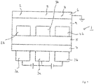
- Fig. 1 shows a schematic representation of an active OLED display 1 having a plurality of OLED pixels 2, 3, 4 provided in an OLED display 1.
- each pixel 2, 3, 4 is provided with an anode 2a, 3a, 4a being connected to a driving circuit (not shown).
- a driving circuit not shown.
- the anodes 2a, 3a, 4a are made of a TCO, for example of ITO.
- a cathode 6 is provided on top of an organic stack comprising an electrically doped hole transport layer (HTL) 7, an electron blocking layer (EBL) 5, a light emitting layer (EML) having sub-regions 2b, 3b, 4b assigned to the pixels 2, 3, 4 and being provided separately in an electron transport layer (ETL) 9.
- the sub-regions 2b, 3b, 4b can provide an RGB combination for a color display (R - red, G - green, B - blue).
- Step 2 lithium tris(4,5,6,7-tetrafluoro-3-(trifluoromethyl)-1H-indazol-1-yl)hydroborate
- Step 1 4,5,6,7-tetrafluoro-3-(perfluorophenyl)-1H-indazole
- Step 2 lithium tris(4,5,6,7-tetrafluoro-3-(perfluorophenyl)-1H-indazol-1-yl)hydroborate
- the pressure tube is closed and heated to a temperature about 160 °C for ca 21 h. After cooling to room temperature, the mixture is treated with 5 mL hexane in an ultra-sonic bath for ca 30 min. The precipitated solid is filtered off and washed with hexane (20 mL in total). After drying, 0.48 g yellowish solid is obtained.
- Example 1 tandem OLED, model for bottom emitting white OLED pixel
- VTE vacuum thermal evaporation
- Example 2 bottom emitting blue OLED pixel
- VTE 10 nm hole injection layer made of the compound PB-1; 120 nm thick HTL made of neat F1; 20 nm EML made of ABH113 doped with 3 wt% NUBD370 (both supplied by SFC, Korea), 36 nm EIL/ETL made of F2 doped with 50 wt% LiQ; 100 nm Al cathode.
- Comparative device comprised the HIL made of the compound CN-HAT (CAS 105598-27-4) instead of PB-1.
- the inventive device achieved current density 15 mA/cm 2 and EQE 5.4 % at a voltage 5.2 V, whereas the comparative device operated at 5.4 V with EQE 4.9 %.
- Table 1 auxiliary materials Compound Structure F1 (CAS 1242056-42-3) F2 (CAS 1440545-225-1) F3 (CAS 597578-38-6) F4 (CAS 1207671-22-4) PD2 2,2',2"-(cyclopropane-1,2,3-triylidene)-tris[2-(4-cyanoperfluorophenyl)-acetonitrile] (CAS1224447-88-4) LiQ 8-Hydroxyquinolato lithium (CAS 850918-68-2) CN-HAT (CAS 105598-27-4)
Landscapes
- Physics & Mathematics (AREA)
- Optics & Photonics (AREA)
- Electroluminescent Light Sources (AREA)
Priority Applications (45)
| Application Number | Priority Date | Filing Date | Title |
|---|---|---|---|
| EP17156904.9A EP3364477A1 (fr) | 2017-02-20 | 2017-02-20 | Dispositif électronique à semi-conducteur et son procédé de préparation |
| JP2019545368A JP7082984B2 (ja) | 2017-02-20 | 2018-02-16 | 電子半導体デバイスおよびその電子半導体デバイスの製造方法および化合物 |
| US16/485,824 US11539014B2 (en) | 2017-02-20 | 2018-02-16 | Electronic semiconducting device, method for preparing the electronic semiconducting device and compound |
| KR1020197027314A KR102478039B1 (ko) | 2017-02-20 | 2018-02-16 | 전자 반도전성 소자, 전자 반도전성 소자를 제조하기 위한 방법, 및 화합물 |
| CN201880012552.0A CN110447117B (zh) | 2017-02-20 | 2018-02-16 | 电子半导体器件,电子半导体器件的制备方法和化合物 |
| PCT/EP2018/053954 WO2018150006A1 (fr) | 2017-02-20 | 2018-02-16 | Dispositif électronique à semiconducteur, son procédé de préparation et composé |
| EP18704265.0A EP3583636B1 (fr) | 2017-02-20 | 2018-02-16 | Dispositif elelctronique procede de fabrication et compose |
| KR1020197027323A KR102677446B1 (ko) | 2017-02-20 | 2018-02-20 | 전자 반도전성 소자 및 전자 반도전성 소자를 제조하기 위한 방법 |
| CN201880012814.3A CN110462872B (zh) | 2017-02-20 | 2018-02-20 | 电子器件、所述电子器件的制备方法和包含所述电子器件的显示装置 |
| CN201880012559.2A CN110462871B (zh) | 2017-02-20 | 2018-02-20 | 电子半导体器件和制备所述电子半导体器件的方法 |
| EP22171384.5A EP4057369B1 (fr) | 2017-02-20 | 2018-02-20 | Écran delo actif, procédé de préparation d'un écran delo actif et composé |
| JP2019544850A JP7305544B2 (ja) | 2017-02-20 | 2018-02-20 | 電子半導体デバイスおよびその製造方法 |
| PCT/EP2018/054154 WO2018150048A1 (fr) | 2017-02-20 | 2018-02-20 | Dispositif semi-conducteur électronique et procédé de préparation de ce dispositif semi-conducteur électronique |
| KR1020197027288A KR102516665B1 (ko) | 2017-02-20 | 2018-02-20 | 전자 장치, 이를 제조하는 방법 및 이를 포함하는 디스플레이 장치 |
| US16/485,813 US11522150B2 (en) | 2017-02-20 | 2018-02-20 | Electronic device, method for preparing the same and display device comprising the same |
| US16/485,839 US11201306B2 (en) | 2017-02-20 | 2018-02-20 | Active OLED display, method for preparing an active OLED display and compound |
| EP25195136.4A EP4629808A3 (fr) | 2017-02-20 | 2018-02-20 | Dispositif semi-conducteur électronique et procédé de préparation du dispositif semi-conducteur électronique |
| US16/485,808 US11239440B2 (en) | 2017-02-20 | 2018-02-20 | Electronic semiconducting device and method for preparing the electronic semiconducting device |
| KR1020197027280A KR102519014B1 (ko) | 2017-02-20 | 2018-02-20 | 전자 반도전성 소자 및 전자 반도전성 소자를 제조하기 위한 방법 |
| JP2019545350A JP2020508580A (ja) | 2017-02-20 | 2018-02-20 | アクティブoledディスプレイ、アクティブoledディスプレイの製造方法および化合物 |
| JP2019544860A JP6999684B2 (ja) | 2017-02-20 | 2018-02-20 | 電子デバイス、当該電子デバイスを製造するための方法、ならびに当該電子デバイスを含むディスプレイデバイス |
| DE112018000908.4T DE112018000908B4 (de) | 2017-02-20 | 2018-02-20 | Elektronische Vorrichtung, Verfahren zum Herstellen derselben und Anzeigevorrichtung, die dieselbe umfasst |
| CN201880013739.2A CN110521015B (zh) | 2017-02-20 | 2018-02-20 | 有源oled显示器、制备有源oled显示器的方法和化合物 |
| CN202211016963.1A CN115377309A (zh) | 2017-02-20 | 2018-02-20 | 有源oled显示器、制备有源oled显示器的方法和化合物 |
| CN202210672671.7A CN115241374A (zh) | 2017-02-20 | 2018-02-20 | 电子半导体器件和制备所述电子半导体器件的方法 |
| KR1020197027327A KR102690851B1 (ko) | 2017-02-20 | 2018-02-20 | 활성 oled 디스플레이, 활성 oled 디스플레이를 제조하기 위한 방법 및 화합물 |
| KR1020247025441A KR20240119182A (ko) | 2017-02-20 | 2018-02-20 | 활성 oled 디스플레이, 활성 oled 디스플레이를 제조하기 위한 방법 및 화합물 |
| JP2019544861A JP7373994B2 (ja) | 2017-02-20 | 2018-02-20 | 電子半導体デバイスおよびその製造方法 |
| US16/485,816 US11322710B2 (en) | 2017-02-20 | 2018-02-20 | Electronic semiconducting device and method for preparing the electronic semiconducting device |
| CN201880012813.9A CN110521014B (zh) | 2017-02-20 | 2018-02-20 | 电子半导体器件和制备电子半导体器件的方法 |
| PCT/EP2018/054162 WO2018150051A1 (fr) | 2017-02-20 | 2018-02-20 | Dispositif semiconducteur électronique et procédé de préparation du dispositif semiconducteur électronique |
| EP18706499.3A EP3583637B1 (fr) | 2017-02-20 | 2018-02-20 | Écran delo actif, procédé de préparation d'un écran delo actif et composé |
| EP18706500.8A EP3583638B1 (fr) | 2017-02-20 | 2018-02-20 | Dispositif électronique à semi-conducteur et son procédé de préparation |
| DE112018000907.6T DE112018000907B4 (de) | 2017-02-20 | 2018-02-20 | Elektronische Halbleitervorrichtung und Verfahren zur Herstellung der elektronischen Halbleitervorrichtung |
| PCT/EP2018/054157 WO2018150049A1 (fr) | 2017-02-20 | 2018-02-20 | Dispositif électronique, son procédé de fabrication et dispositif d'affichage le comprenant |
| PCT/EP2018/054160 WO2018150050A1 (fr) | 2017-02-20 | 2018-02-20 | Affichage à oled actif, procédé de préparation d'un affichage à oled actif et composé |
| TW107105848A TWI762586B (zh) | 2017-02-20 | 2018-02-21 | 電子半導體元件及其製備方法 |
| TW107105851A TWI806851B (zh) | 2017-02-20 | 2018-02-21 | 主動oled顯示器及備製主動oled顯示器方法 |
| TW107105850A TWI761457B (zh) | 2017-02-20 | 2018-02-21 | 電子半導體元件及其製備方法 |
| TW107105849A TWI753111B (zh) | 2017-02-20 | 2018-02-21 | 電子元件、其備製方法及含該元件之顯示裝置 |
| US17/519,446 US20220059787A1 (en) | 2017-02-20 | 2021-11-04 | Active OLED Display, Method for Preparing an Active OLED Display and Compound |
| US17/659,565 US11825667B2 (en) | 2017-02-20 | 2022-04-18 | Electronic semiconducting device and method for preparing the electronic semiconducting device |
| US17/881,878 US12022672B2 (en) | 2017-02-20 | 2022-08-05 | Electronic semiconducting device, method for preparing the electronic semiconducting device and compound |
| JP2022144426A JP7447209B2 (ja) | 2017-02-20 | 2022-09-12 | アクティブoledディスプレイ、アクティブoledディスプレイの製造方法および化合物 |
| JP2022178073A JP7541563B2 (ja) | 2017-02-20 | 2022-11-07 | 電子半導体デバイスおよびその製造方法 |
Applications Claiming Priority (1)
| Application Number | Priority Date | Filing Date | Title |
|---|---|---|---|
| EP17156904.9A EP3364477A1 (fr) | 2017-02-20 | 2017-02-20 | Dispositif électronique à semi-conducteur et son procédé de préparation |
Publications (2)
| Publication Number | Publication Date |
|---|---|
| EP3364477A1 true EP3364477A1 (fr) | 2018-08-22 |
| EP3364477A8 EP3364477A8 (fr) | 2018-12-19 |
Family
ID=58158827
Family Applications (1)
| Application Number | Title | Priority Date | Filing Date |
|---|---|---|---|
| EP17156904.9A Withdrawn EP3364477A1 (fr) | 2017-02-20 | 2017-02-20 | Dispositif électronique à semi-conducteur et son procédé de préparation |
Country Status (1)
| Country | Link |
|---|---|
| EP (1) | EP3364477A1 (fr) |
Cited By (4)
| Publication number | Priority date | Publication date | Assignee | Title |
|---|---|---|---|---|
| CN110931649A (zh) * | 2019-11-29 | 2020-03-27 | 昆山国显光电有限公司 | 一种有机电致发光器件及显示装置 |
| CN113937223A (zh) * | 2021-12-15 | 2022-01-14 | 江西省科学院应用化学研究所 | 一种功能分子共掺杂钙钛矿太阳能电池的制备方法 |
| US11522150B2 (en) | 2017-02-20 | 2022-12-06 | Novaled Gmbh | Electronic device, method for preparing the same and display device comprising the same |
| EP4356447A1 (fr) | 2021-06-18 | 2024-04-24 | Novaled GmbH | Procédé de préparation d'une couche semi-conductrice de type p, couche semi-conductrice de type p, dispositif électronique organique, dispositif d'affichage, composé métallique et utilisation dudit composé métallique |
Citations (8)
| Publication number | Priority date | Publication date | Assignee | Title |
|---|---|---|---|---|
| EP0510541A1 (fr) * | 1991-04-19 | 1992-10-28 | Mitsubishi Chemical Corporation | Dispositif électroluminescent organique |
| EP1970371A1 (fr) | 2007-03-16 | 2008-09-17 | Novaled AG | Pyrido(3,2-h)chinazoline et/ou leurs dérivés 5,6-dihydro, leur procédé de fabrication et matériau semi-conducteur organique en étant doté |
| WO2011134458A1 (fr) | 2010-04-27 | 2011-11-03 | Novaled Ag | Matériau semi-conducteur organique et composant électronique |
| US20120223296A1 (en) | 2011-03-01 | 2012-09-06 | Sensient Imaging Technologies Gmbh | Organic Semiconducting Materials and Organic Component |
| WO2013079217A1 (fr) | 2011-11-30 | 2013-06-06 | Novaled Ag | Afficheur |
| WO2013135237A1 (fr) | 2012-03-15 | 2013-09-19 | Novaled Ag | Composés aromatiques amino-triphényles et utilisation desdits composés dans des composants semi-conducteurs organiques |
| WO2014060526A1 (fr) | 2012-10-17 | 2014-04-24 | Novaled Gmbh | Delo phosphorescente et matériaux de transport de trous pour delo phosphorescentes |
| WO2016050834A1 (fr) | 2014-09-30 | 2016-04-07 | Novaled Gmbh | Écran oled actif, procédé de fonctionnement d'un écran oled actif et composé |
-
2017
- 2017-02-20 EP EP17156904.9A patent/EP3364477A1/fr not_active Withdrawn
Patent Citations (8)
| Publication number | Priority date | Publication date | Assignee | Title |
|---|---|---|---|---|
| EP0510541A1 (fr) * | 1991-04-19 | 1992-10-28 | Mitsubishi Chemical Corporation | Dispositif électroluminescent organique |
| EP1970371A1 (fr) | 2007-03-16 | 2008-09-17 | Novaled AG | Pyrido(3,2-h)chinazoline et/ou leurs dérivés 5,6-dihydro, leur procédé de fabrication et matériau semi-conducteur organique en étant doté |
| WO2011134458A1 (fr) | 2010-04-27 | 2011-11-03 | Novaled Ag | Matériau semi-conducteur organique et composant électronique |
| US20120223296A1 (en) | 2011-03-01 | 2012-09-06 | Sensient Imaging Technologies Gmbh | Organic Semiconducting Materials and Organic Component |
| WO2013079217A1 (fr) | 2011-11-30 | 2013-06-06 | Novaled Ag | Afficheur |
| WO2013135237A1 (fr) | 2012-03-15 | 2013-09-19 | Novaled Ag | Composés aromatiques amino-triphényles et utilisation desdits composés dans des composants semi-conducteurs organiques |
| WO2014060526A1 (fr) | 2012-10-17 | 2014-04-24 | Novaled Gmbh | Delo phosphorescente et matériaux de transport de trous pour delo phosphorescentes |
| WO2016050834A1 (fr) | 2014-09-30 | 2016-04-07 | Novaled Gmbh | Écran oled actif, procédé de fonctionnement d'un écran oled actif et composé |
Non-Patent Citations (5)
| Title |
|---|
| CHUNG ET AL.: "Invited Paper: Large-Sized Full Color AMOLED TV: Advancements and Issues", SID SYMPOSIUM DIGEST OF TECHNICAL PAPERS, vol. 37, 2006, pages 1958 - 1963 |
| JIANGBIN XIA ET AL: "Influence of Doped Anions on Poly(3,4-ethylenedioxythiophene) as Hole Conductors for Iodine-Free Solid-State Dye-Sensitized Solar Cells", THE JOURNAL OF THE AMERICAN CHEMICAL SOCIETY, vol. 130, 3 January 2008 (2008-01-03), pages 1258 - 1263, XP055002033, DOI: 10.1021/ja075704o * |
| JOURNAL OF ORGANIC CHEMISTRY, vol. 76, no. 2, 2011, pages 391 - 395 |
| LEE ET AL.: "Development of -Inch Full-HD AMOLED TV Using LTPS-TFT and RGB FMM", SID SYMPOSIUM DIGEST OF TECHNICAL PAPERS, vol. 40, 2009, pages 802 - 804, XP007017188 |
| MENKE TORBEN ET AL: "Highly efficientp-dopants in amorphous hosts", ORGANIC ELECTRONICS, ELSEVIER, AMSTERDAM, NL, vol. 15, no. 2, 2 December 2013 (2013-12-02), pages 365 - 371, XP028817910, ISSN: 1566-1199, DOI: 10.1016/J.ORGEL.2013.11.033 * |
Cited By (7)
| Publication number | Priority date | Publication date | Assignee | Title |
|---|---|---|---|---|
| US11522150B2 (en) | 2017-02-20 | 2022-12-06 | Novaled Gmbh | Electronic device, method for preparing the same and display device comprising the same |
| US11825667B2 (en) | 2017-02-20 | 2023-11-21 | Novaled Gmbh | Electronic semiconducting device and method for preparing the electronic semiconducting device |
| US12022672B2 (en) | 2017-02-20 | 2024-06-25 | Novaled Gmbh | Electronic semiconducting device, method for preparing the electronic semiconducting device and compound |
| CN110931649A (zh) * | 2019-11-29 | 2020-03-27 | 昆山国显光电有限公司 | 一种有机电致发光器件及显示装置 |
| CN110931649B (zh) * | 2019-11-29 | 2022-11-15 | 昆山国显光电有限公司 | 一种有机电致发光器件及显示装置 |
| EP4356447A1 (fr) | 2021-06-18 | 2024-04-24 | Novaled GmbH | Procédé de préparation d'une couche semi-conductrice de type p, couche semi-conductrice de type p, dispositif électronique organique, dispositif d'affichage, composé métallique et utilisation dudit composé métallique |
| CN113937223A (zh) * | 2021-12-15 | 2022-01-14 | 江西省科学院应用化学研究所 | 一种功能分子共掺杂钙钛矿太阳能电池的制备方法 |
Also Published As
| Publication number | Publication date |
|---|---|
| EP3364477A8 (fr) | 2018-12-19 |
Similar Documents
| Publication | Publication Date | Title |
|---|---|---|
| US12022672B2 (en) | Electronic semiconducting device, method for preparing the electronic semiconducting device and compound | |
| EP3364477A1 (fr) | Dispositif électronique à semi-conducteur et son procédé de préparation | |
| EP3364476B1 (fr) | Écran delo actif, procédé de préparation d'un écran delo actif et composé | |
| EP3364475B1 (fr) | Dispositif elelctronique procede de fabrication et compose |
Legal Events
| Date | Code | Title | Description |
|---|---|---|---|
| PUAI | Public reference made under article 153(3) epc to a published international application that has entered the european phase |
Free format text: ORIGINAL CODE: 0009012 |
|
| AK | Designated contracting states |
Kind code of ref document: A1 Designated state(s): AL AT BE BG CH CY CZ DE DK EE ES FI FR GB GR HR HU IE IS IT LI LT LU LV MC MK MT NL NO PL PT RO RS SE SI SK SM TR |
|
| AX | Request for extension of the european patent |
Extension state: BA ME |
|
| STAA | Information on the status of an ep patent application or granted ep patent |
Free format text: STATUS: THE APPLICATION IS DEEMED TO BE WITHDRAWN |
|
| RAP1 | Party data changed (applicant data changed or rights of an application transferred) |
Owner name: NOVALED GMBH |
|
| 18D | Application deemed to be withdrawn |
Effective date: 20190223 |