EP3364728A1 - Film de câblage, feuille de transfert de dispositif, et dispositif type textile - Google Patents
Film de câblage, feuille de transfert de dispositif, et dispositif type textile Download PDFInfo
- Publication number
- EP3364728A1 EP3364728A1 EP16855525.8A EP16855525A EP3364728A1 EP 3364728 A1 EP3364728 A1 EP 3364728A1 EP 16855525 A EP16855525 A EP 16855525A EP 3364728 A1 EP3364728 A1 EP 3364728A1
- Authority
- EP
- European Patent Office
- Prior art keywords
- wiring
- film
- wirings
- wiring film
- layer
- Prior art date
- Legal status (The legal status is an assumption and is not a legal conclusion. Google has not performed a legal analysis and makes no representation as to the accuracy of the status listed.)
- Withdrawn
Links
Images





Classifications
-
- H—ELECTRICITY
- H05—ELECTRIC TECHNIQUES NOT OTHERWISE PROVIDED FOR
- H05K—PRINTED CIRCUITS; CASINGS OR CONSTRUCTIONAL DETAILS OF ELECTRIC APPARATUS; MANUFACTURE OF ASSEMBLAGES OF ELECTRICAL COMPONENTS
- H05K1/00—Printed circuits
- H05K1/02—Details
- H05K1/03—Use of materials for the substrate
- H05K1/038—Textiles
-
- A—HUMAN NECESSITIES
- A61—MEDICAL OR VETERINARY SCIENCE; HYGIENE
- A61B—DIAGNOSIS; SURGERY; IDENTIFICATION
- A61B5/00—Measuring for diagnostic purposes; Identification of persons
- A61B5/02—Detecting, measuring or recording for evaluating the cardiovascular system, e.g. pulse, heart rate, blood pressure or blood flow
- A61B5/0205—Simultaneously evaluating both cardiovascular conditions and different types of body conditions, e.g. heart and respiratory condition
-
- A—HUMAN NECESSITIES
- A61—MEDICAL OR VETERINARY SCIENCE; HYGIENE
- A61B—DIAGNOSIS; SURGERY; IDENTIFICATION
- A61B5/00—Measuring for diagnostic purposes; Identification of persons
- A61B5/68—Arrangements of detecting, measuring or recording means, e.g. sensors, in relation to patient
- A61B5/6801—Arrangements of detecting, measuring or recording means, e.g. sensors, in relation to patient specially adapted to be attached to or worn on the body surface
- A61B5/6802—Sensor mounted on worn items
- A61B5/6804—Garments; Clothes
- A61B5/6805—Vests, e.g. shirts or gowns
-
- H—ELECTRICITY
- H05—ELECTRIC TECHNIQUES NOT OTHERWISE PROVIDED FOR
- H05K—PRINTED CIRCUITS; CASINGS OR CONSTRUCTIONAL DETAILS OF ELECTRIC APPARATUS; MANUFACTURE OF ASSEMBLAGES OF ELECTRICAL COMPONENTS
- H05K1/00—Printed circuits
- H05K1/02—Details
-
- H—ELECTRICITY
- H05—ELECTRIC TECHNIQUES NOT OTHERWISE PROVIDED FOR
- H05K—PRINTED CIRCUITS; CASINGS OR CONSTRUCTIONAL DETAILS OF ELECTRIC APPARATUS; MANUFACTURE OF ASSEMBLAGES OF ELECTRICAL COMPONENTS
- H05K1/00—Printed circuits
- H05K1/02—Details
- H05K1/03—Use of materials for the substrate
- H05K1/0393—Flexible materials
-
- H—ELECTRICITY
- H10—SEMICONDUCTOR DEVICES; ELECTRIC SOLID-STATE DEVICES NOT OTHERWISE PROVIDED FOR
- H10W—GENERIC PACKAGES, INTERCONNECTIONS, CONNECTORS OR OTHER CONSTRUCTIONAL DETAILS OF DEVICES COVERED BY CLASS H10
- H10W70/00—Package substrates; Interposers; Redistribution layers [RDL]
- H10W70/60—Insulating or insulated package substrates; Interposers; Redistribution layers
-
- H—ELECTRICITY
- H10—SEMICONDUCTOR DEVICES; ELECTRIC SOLID-STATE DEVICES NOT OTHERWISE PROVIDED FOR
- H10W—GENERIC PACKAGES, INTERCONNECTIONS, CONNECTORS OR OTHER CONSTRUCTIONAL DETAILS OF DEVICES COVERED BY CLASS H10
- H10W70/00—Package substrates; Interposers; Redistribution layers [RDL]
- H10W70/60—Insulating or insulated package substrates; Interposers; Redistribution layers
- H10W70/67—Insulating or insulated package substrates; Interposers; Redistribution layers characterised by their insulating layers or insulating parts
- H10W70/68—Shapes or dispositions thereof
-
- H—ELECTRICITY
- H10—SEMICONDUCTOR DEVICES; ELECTRIC SOLID-STATE DEVICES NOT OTHERWISE PROVIDED FOR
- H10W—GENERIC PACKAGES, INTERCONNECTIONS, CONNECTORS OR OTHER CONSTRUCTIONAL DETAILS OF DEVICES COVERED BY CLASS H10
- H10W70/00—Package substrates; Interposers; Redistribution layers [RDL]
- H10W70/60—Insulating or insulated package substrates; Interposers; Redistribution layers
- H10W70/67—Insulating or insulated package substrates; Interposers; Redistribution layers characterised by their insulating layers or insulating parts
- H10W70/69—Insulating materials thereof
-
- H—ELECTRICITY
- H10—SEMICONDUCTOR DEVICES; ELECTRIC SOLID-STATE DEVICES NOT OTHERWISE PROVIDED FOR
- H10W—GENERIC PACKAGES, INTERCONNECTIONS, CONNECTORS OR OTHER CONSTRUCTIONAL DETAILS OF DEVICES COVERED BY CLASS H10
- H10W70/00—Package substrates; Interposers; Redistribution layers [RDL]
- H10W70/60—Insulating or insulated package substrates; Interposers; Redistribution layers
- H10W70/67—Insulating or insulated package substrates; Interposers; Redistribution layers characterised by their insulating layers or insulating parts
- H10W70/69—Insulating materials thereof
- H10W70/695—Organic materials
-
- A—HUMAN NECESSITIES
- A41—WEARING APPAREL
- A41D—OUTERWEAR; PROTECTIVE GARMENTS; ACCESSORIES
- A41D1/00—Garments
- A41D1/002—Garments adapted to accommodate electronic equipment
- A41D1/005—Garments adapted to accommodate electronic equipment with embedded cable or connector
-
- A—HUMAN NECESSITIES
- A61—MEDICAL OR VETERINARY SCIENCE; HYGIENE
- A61B—DIAGNOSIS; SURGERY; IDENTIFICATION
- A61B2562/00—Details of sensors; Constructional details of sensor housings or probes; Accessories for sensors
- A61B2562/16—Details of sensor housings or probes; Details of structural supports for sensors
- A61B2562/164—Details of sensor housings or probes; Details of structural supports for sensors the sensor is mounted in or on a conformable substrate or carrier
Definitions
- An embodiment of the present invention relates to a wiring film, a device transfer sheet, and a textile type device.
- Patent Document 1 includes a strain-sensor-attached cloth including a strain sensor having a carbon nanotube film attached to a cloth and a wiring part connected to the strain sensor.
- Patent Document 2 includes cloths in which a wiring part is integrally provided on a cloth main body.
- the wiring part is integrated with the cloth main body so that it becomes difficult for the wiring part to be cut and it is possible to minimize interference with a wearer's motion with the device.
- one end of the wirings is connected to an electrode of the sensor but the other portion thereof is not fixed to a base member or the like. For this reason, when the number of wires increases, the wiring itself interferes with the wearer's hand motion or interferes with the wearer's movement.
- the wiring part is directly formed on the cloth main body. Since a thread-like body having conductivity is knitted into the cloth, it cannot be said that conformability with respect to deformation or tension is sufficient. Furthermore, a short circuit between wirings may occur due to contact between wires, with sweat, or the like in some cases. Since the cloth is easily deformed even if it is attempted to adhere insulating layers to both surfaces of the wiring part to prevent a short circuit, it is difficult to position the insulating layers. In addition, there is a concern that impairment of stretchability or air permeability occurs due to the adhered insulating layers.
- the present invention was made in view of the above circumstances, and an object of the present invention is to provide a textile type device in which there is less discomfort at the time of wearing the device and capable of minimizing occurrence of short circuits or the like. Furthermore, an object of the present invention is to provide a wiring pattern which can be suitably used for a device transfer sheet and a device transfer sheet which can be easily attached to a cloth in which the textile type device is deformed.
- the inventors of the present invention found that a device transfer sheet having high flexibility can be obtained by forming wirings in a film having excellent stretchability.
- the inventors found that a textile type device in which there is less discomfort and which causes hardly any problems such as a short circuit at the time of wearing the device using the device transfer sheet can be obtained, thereby completing the present invention.
- the present invention adopts the following means.
- a wiring film according to an embodiment of the present invention can be used as a wiring film for a device transfer sheet because the wiring film has adhesive properties and high stretchability.
- an electronic component in which wirings are provided can be easily transferred to a cloth and a short circuit does not occur in the wirings.
- a textile type device causes less discomfort and hardly any problems such as a short circuit at the time of wearing the device.
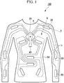
- Fig. 1 is a schematic plan view of a textile type device according to an embodiment of the present invention.
- a textile type device 100 includes a cloth 50, a plurality of electronic components (sensors) 20 provided in the cloth 50, a circuit board 30 in which information from the sensors 20 is integrated, an external output means 40 for outputting the information integrated in the circuit board 30 to the outside, and wirings 11 configured to connect the sensors 20 and the circuit board 30.
- Fig. 2 is a cross-sectional view schematically showing an example of a cross section of the textile type device shown in Fig. 1 taken along surface A-A.
- the wirings 11 are provided in a wiring film 10.
- the wiring film 10 is disposed between the cloth 50 and one of the sensors 20 and a protective layer 21.
- a wiring layer 13 and an adhesive layer 15 constituting the wiring film 10, the sensor 20, the protective layer 21, and the cloth 50 are actually in contact with each other, but are shown by being partially separated for the sake of helping understanding thereof.
- the wiring film 10 shown in Fig. 2 includes the wiring layer 13 and a short-circuit prevention layer 15.
- the wiring layer 13 includes an extensible film 12 and a wirings 11 provided along the extensible film 12 inside or on an outer surface of the extensible film 12.
- a part of the wirings 11 is exposed from at least a first surface 13a of the wiring layer 13 on the sensor 20 side.
- the part of the wirings 11 is exposed from the first surface 13a so that the wiring 11 can be in contact with the sensor 20.
- the wiring film of the present invention in order to bring the wirings into contact with the sensor while securing insulation of the wirings, only a part of the wirings may be exposed from the first surface.
- the wirings are provided inside and on the outer surface of the extensible film.
- stretchable wiring such as a conductive thread, a conductive wire, a conductive ink, or the like
- a "conductive thread” refers to a natural fiber or a chemical fiber coated with a conductive material
- a "conductive wire” refers to a wire-like member made of a conductive material.
- the conductive wire is typically a metallic wire, but is not limited to a metallic wire as long as the conductive wire has conductivity. Particularly, it is desirable to use a conductive thread or a conductive wire for the wirings 11 and it is more desirable to use a conductive thread coated with silver and a copper wire as the conductive thread and the conductive wire, respectively.
- the conductive thread is a thread having conductivity.
- the conductive thread has high durability and high conformability to changes in shape. For this reason, deformation or the like of the textile type device 100 can also be prevented using a conductive thread.
- a copper wire has high conductivity and low variation in resistance.
- conductive threads are used for wirings between sensors like in conventional motion capture and copper wires may be used for wirings of a digital device (in which high conductivity is required) for the purpose of adding further functions.
- the wirings 11 may be used by being coated with an insulating material. In this case, a portion exposed from the first surface of the wiring layer facing the electronic component is not coated with an insulating material.
- a meandering shape can be any shape such as a zigzag, a waveform, a curve obtained by aligning a plurality of horseshoe shapes and/or parts of horseshoe shapes and joining or interpolating between ends thereof, a continuous hairpin curve, a line obtained by combining a plurality of parts of polygons, and a line obtained by combining a plurality of parts of star shapes, or combinations thereof, a substantially straight line and an approximate curve, and combinations of a substantially straight line and an approximate curve.
- a period of meandering and a width of meanders can have any values. Furthermore, meanders may not have the same shapes, the same period, and/or width and may have different values. When the wirings 11 such as the conductive thread or the conductive wire meander, conformability to the deformation of the extensible film 12 can be improved.
- any member having stretchability can be used for the extensible film 12. Since the extensible film 12 stretches and contracts, a textile type device 100 which can conform to deformation such as stretching and bending can be obtained.
- an amount of change in shape with respect to an initial state is preferably 30% or more, more preferably 50% or more, and particularly preferably 100% or more.
- a thickness of the extensible film 12 is not particularly limited, the thickness thereof is preferably 5 ⁇ m to 300 ⁇ m and more preferably 10 ⁇ m to 100 ⁇ m. Both high stretchability and strength can be achieved as long as the thickness of the extensible film 12 is in this range.
- the extensible film 12 is constituted of an adhesive layer 12A and an insulating layer 12B from the first surface side of the extensible film.
- the adhesive layer 12A is thermally melted, the wiring film 10, the sensor 20, and the protective layer 21 can be fused and joined.
- the insulating layer 12B any member having stretchability such as a polyurethane film can be used.
- the adhesive layer 12A is preferably a thermoplastic adhesive layer and examples of thermoplastic adhesive layer include known hot melt films and the like, but it is desirable that the adhesive layer 12A be a hot melt film having stretchability.
- a hot melt having stretchability examples include a hot melt film or the like having polyurethane as a main ingredient.
- a conductive hot melt containing conductive metal particles may be partially used between contact points of the sensor 20 and the wirings 11. Thus, an electrical connection between the sensor 20 and the wirings 11 can be improved so that contact resistance is reduced.
- conductive metallic fine particles used for the conductive hot melt silver, gold, copper, platinum, or aluminum is preferable, silver, gold, or copper is more preferable, and silver is most preferable. Furthermore, using flake-like metallic fine particles, high conductivity can be imparted with a small content. It is desirable that the conductive hot melt include a hot melt having polyurethane as a main ingredient. Thus, detaching from the sensor 20 or the wirings 11 due to distortion applied at the time of the cloth stretching and contracting can be minimized.
- the extensible film 12 is not limited to this embodiment.
- the extensible film 12 may be constituted only of the insulating layer 12B made of a polyurethane film, adhesive layers may be formed on both surfaces of the insulating layer 12B, and the extensible film 12 may be constituted only of an adhesive layer. Modifications thereof will be described below in detail.
- the short-circuit prevention layer 15 is disposed on a second surface 13b of the wiring layer 13 opposite to the first surface 13a. In the wiring layer 13, if the wirings 11 are not exposed from the second surface 13b, the short-circuit prevention layer 15 may be omitted. However, as the short-circuit prevention layer 15 is provided on the second surface 13b of the wiring layer 13, a short circuit due to penetration of sweat or the like from the cloth 50 can be more effectively prevented.
- the present invention can also be used underwater or the like.
- the short-circuit prevention layer 15 also has a function of adhering the wiring layer 13 to the cloth 50.
- the textile type device 100 functions as a wearable device. For this reason, it is assumed that washing or the like is performed. Since the short-circuit prevention layer 15 firmly adheres the wiring layer 13 to the cloth 50, detaching of the short-circuit prevention layer 15 can be prevented when treatment using water such as washing is performed.
- the short-circuit prevention layer 15 have the first surface 15a thereof on the wiring layer 13 side and a second surface 15b thereof opposite to the first surface 15a and have at least an adhesive layer 15C on the second surface 15b.
- FIG. 2 an example in which an adhesive layer 15A and the adhesive layer 15C are provided on both surfaces of an insulating layer 15B is shown.
- thermoplastic adhesive layers be used for the adhesive layers 15A and 15C.
- conformability at the time of the cloth stretching and contracting can be improved and the wiring layer 13 and the cloth 50 are firmly adhered.
- thermoplastic adhesive layer include a known hot melt film or the like, but it is desirably a hot melt film having stretchability.
- a hot melt having stretchability include a hot melt or the like having polyurethane as a main ingredient.
- the short-circuit prevention layer 15 includes the insulating layer 15B
- the short-circuit prevention layer 15 can embed the wirings 11 exposed from the second surface 13b of the wiring layer 13 on the cloth 50 side, thereby further improving insulating properties.
- short circuiting of the textile type device due to sweat or the like can be minimized.
- the strength of the entire wiring film 10 can be further increased. It is desirable to use a polyurethane film as the insulating layer 15B. Thus, high insulation properties can be ensured and conformability at the time of the cloth stretching and contracting is improved.
- a thickness of the short-circuit prevention layer 15 is not particularly limited, but is preferably 10 ⁇ m to 800 ⁇ m and more preferably 30 ⁇ m to 300 ⁇ m.
- a thickness of the insulating layer 15B is preferably 5 ⁇ m to 300 ⁇ m and more preferably 10 ⁇ m to 100 ⁇ m. High stretchability and strength can be maintained as long as the thickness of the insulating layer 15B is in this range.
- Thicknesses of the adhesive layers 15A and 15C are preferably 10 ⁇ m to 200 ⁇ m and more preferably 30 ⁇ m to 100 ⁇ m. When the thickness of the adhesive layer 15C is within this range, the cloth and the wiring film 10 can be strongly adhered to each other and can be used for a long period of time without becoming detached due to washing or the like.
- the wiring film 10 constituted of the wiring layer 13 and the short-circuit prevention layer 15 preferably has a conductivity when a shape thereof has changed by 10% or more that is 1/10 to 10 times a conductivity when the shape thereof has not changed. Furthermore, it is desirable that a proportion of conductivity change be kept in this range even if the shape thereof changes by 30% or more, it is more desirable that the proportion of conductivity change be kept in this range even if the shape thereof changes by 50% or more, and it is particularly desirable that the proportion of conductivity change be kept in this range even if the shape thereof changes by 100% or more.
- a short-circuit prevention layer 15 is not limited to this example and various constitutions thereof can be adopted.
- the short-circuit prevention layer may also serve as a thermoplastic adhesive layer.
- the short-circuit prevention layer 15 may be constituted of a more plurality of layers.
- Examples of the sensor 20 include a photodiode, a temperature sensor, a strain sensor, a pressure sensor, and the like. In addition, different sensors may be used for different places. Depending on usage applications, the sensor 20 may be replaced with an electronic component other than a sensor.
- the sensor 20 is not particularly limited as long as a current or a voltage of the sensor changes due to a change in a physical quantity, but is preferably a variable resistance type sensor whose resistance varies depending on a physical quantity and a voltage of which at both ends changes, due to the simplicity or the like of a circuit.
- the physical quantity at least one of the group consisting of sound, light, temperature, pressure, and strain can be suitably used.
- a resistance value of the resistance of the sensor 20 is preferably 50 times or more a wiring resistance of the wirings 11.
- a distance between the sensor 20 and an external output means 5 differs depending on a location, but the resistance of the sensor 20 is set to a value that is 50 times or more the wiring resistance so that an influence of the wiring resistance of the wirings 11 can be eliminated.
- a sensor using ink is a sensor prepared using ink obtained by mixing conductive particles with an elastomer solution or a dispersion. By printing and drying this ink, a sensor in which the conductive particles are randomly dispersed in an elastomer film is obtained. In the sensor, distances between conductive particles change in accordance with thermal expansion/contraction due to tension, compression, and change in temperature and thus the resistance between both ends of the sensor changes.
- a sensor using ink is very thin and conformability to an object on which measurement is to be performed is high. For this reason, accurate and stable measurement can be performed.
- the protective layer 21 covers the wiring film 10 and the sensor 20 in a plan view.
- a surface 21b of the protective layer 21 on a side opposite to a surface 21a on which the sensor 20 is provided is an outermost surface in a state of being used.
- the wiring film 10 and the sensor 20 are covered with the protective layer 21 so that the wirings 11 can be embedded in a device transfer sheet 100.
- the wiring film 10 can be protected from erosion due to sweat or the like when a textile type device obtained using the device transfer sheet 100 is used.
- the textile type device can also be used underwater.
- the protective layer 21 is the outermost surface when the textile type device is used as described above. For this reason, it is desirable that the protective layer 21 have insulating properties and stretchability. In addition, it is desirable that the protective layer 21 be a layer made of polyurethane.
- a thickness of the protective layer 21 is preferably 5 ⁇ m to 300 ⁇ m and more preferably 10 ⁇ m to 100 ⁇ m. High stretchability and strength can be maintained as long as the thickness of the protective layer 21 is in this range.
- Fig. 3 is a cross-sectional view schematically showing an example of a cross section of the textile type device shown in Fig. 1 taken along surface B-B.
- the protective layer 21 and the wiring film 10 (wiring layer 13 and short-circuit prevention layer 15) be provided only in a portion along the wirings 11 constituting the sensor 20 and the wiring film 10 in a plan view.
- the protective layer 21 and the wiring film 10 are provided only in a necessary minimum portion along the wirings 11 in this way so that a space K to which nothing is attached is formed above the cloth 50. Due to the presence of the space K, air permeability and flexibility of the textile type device 100 can be further improved.
- the portions along the sensor 20 and the wirings 11 are preferably in a range of 0.1 mm to 100 mm from outer peripheries of the sensor 20 and the wirings 11 in a plan view and more preferably 0.5 mm to 5 mm. If the portions along the sensor 20 and the wirings 11 are too large, there are more unnecessary portions and thus air permeability of the textile type device is hindered. On the other hand, if the portions along the sensor 20 and the wirings 11 are too narrow, a part of the sensor 20 and the wirings 11 is highly likely to be exposed to the outside due to a level difference between the sensor 20 and the wirings 11 and a short circuit is highly likely to occur.
- cloths can be used as the cloth 50.
- existing cloths may be used as the cloth 50. Since a sensitivity of the sensor 20 can be increased when the sensor 20 is in close contact with a person, it is desirable that the cloth 50 be made of a stretchable material.
- the circuit board 30 is a part configured to collect information from sensors attached to various portions.
- circuit board 30 known boards can be used.
- a flexible printed circuit board or the like can be used.
- the external output means 40 is a part configured to output electrical information from the sensor 20 to the outside.
- the external output means 40 may be a wired communication device or a wireless communication device as long as the external output means 40 can transmit a signal to the outside. From the viewpoint of reducing discomfort at the time of wearing, it is desirably a wireless communication device.
- a communication standard such as Bluetooth (registered trademark), Zigbee (registered trademark), and Wi-Fi (registered trademark) can be used.
- a microcomputer, a lithium battery, and the like may also be installed in the external output means.
- Fig. 4 shows a modification and is a cross-sectional view corresponding to a cross section of the textile type device shown in Fig. 1 taken along surface A-A.
- a textile type device 101 shown in Fig. 4 a wiring layer 12 and a short-circuit prevention layer 15 constituting a wiring film 10 have different constitutions.
- Other constituents are the same as those of the above-described textile type device 100 and are denoted with the same reference numerals.
- an extensible film 12 has three layers and the short-circuit prevention layer 15 has two layers.
- the extensible film 12 is constituted of an insulating layer 12B having adhesive layers 12C and 12F on both surfaces thereof.
- the short-circuit prevention layer 15 is constituted of an insulating layer 15D having an adhesive layer 15E on a surface thereof on a cloth 50 side.
- the textile type device 101 since a part of the wirings 11 is exposed from a first surface 13a of a wiring layer 13, application of electricity to the sensor 20 can be secured. Since the short-circuit prevention layer 15 is arranged on a portion of the wiring layer 13 on the cloth 50 side, penetration of sweat or the like from the cloth 50 can be prevented. In other words, a short circuit caused by sweat or the like can be prevented.
- Fig. 5 shows another modification and is a cross-sectional view corresponding to a cross section of the textile type device shown in Fig. 1 taken along surface A-A.
- a textile type device 102 shown in Fig. 5 and the above-described textile type device 101 differ in that, in the textile type device 102, an adhesive layer 22 having the same function as that of the adhesive layer 12C of the wiring layer 13 in the above-described textile type device 101 arranged on the sensor 20 side is arranged on the sensor 20 and protective layer 21 sides.
- Other constituents are the same as those of the above-described textile type device 100 and denoted with the same reference numerals.
- connection is possible without any problem as long as the adhesive layer 22 can be sufficiently melted by heat or the like at the time of adhering.
- application of electricity to the wirings 11 and the sensor 20 can be secured and penetration of sweat or the like from a cloth 50 can be prevented.
- a short circuit caused by sweat or the like can be prevented.
- Fig. 6 shows yet another modification and is a cross-sectional view corresponding to a cross section of the textile type device shown in Fig. 1 taken along surface A-A.
- a textile type device 103 shown in Fig. 6 and the above-described textile type device 100 differ in that, in the textile type device 103, an adhesive layer 22 having the same function as that of the adhesive layer 12A of the wiring layer 13 in the textile type device 100 arranged on the sensor 20 side is arranged on the sensor 20 and protective layer 21 sides.
- Other constituents are the same as those of the above-described textile type device 100 and denoted with the same reference numerals.
- connection is possible without any problem as long as the adhesive layer 22 can be sufficiently melted by heat or the like at the time of adhering.
- application of electricity to the wirings 11 and the sensor 20 can be secured and penetration of sweat or the like from the cloth 50 can be prevented.
- a short circuit caused by sweat or the like can be prevented.
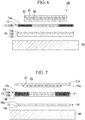
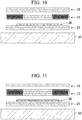
- the short-circuit prevention layer 15 may include only one layer of adhesive layer 15F as shown in Figs. 7 and 9 and the extensible film 12 may include only one layer of an adhesive layer 12F as shown in Figs. 8 and 9 .
- an order of the sensor 20, the wiring layer 13, and the short-circuit prevention layer 15 with respect to the cloth 50 may be reversed.
- the cloth 50, the sensor 20, the wiring layer 13, and the short-circuit prevention layer 15 may be stacked in this order.
- the textile type device according to the embodiment of the present invention is used so that a wearable sensor device can be obtained. Furthermore, short circuiting caused by moisture such as sweat, discomfort due to poor air permeability, and the like can be prevented, thereby allowing a device with less discomfort to the wearer to be provided.
- FIG. 14 is a schematic cross-sectional view of a device transfer sheet according to an embodiment of the present invention.
- a device transfer sheet 200 according to the embodiment of the present invention includes a wiring film 10, a sensor 20, a protective layer 21, and a temporary support 60.
- the device transfer sheet 200 When the device transfer sheet 200 is transferred to a cloth and the temporary support 60 is detached, the device transfer sheet 200 functions as a textile type device of the present invention like the textile type device 100 to 103 described above.
- An example shown in Fig. 14 is a case in which the textile type device 100 is provided, the wiring film 10, the sensor 20, and the protective layer 21 have the same constituents as those of the textile type device 100, and detailed description thereof will be omitted.
- the temporary support 60 is a support part configured to support the wiring film 10, the sensor 20, and the protective layer 21 until the textile type device is transferred to the cloth.
- the temporary support 60 is detached when the textile type device is used.
- a material of the temporary support 60 is not particularly limited.
- a commercially available polyethylene terephthalate (PET) film or the like can be used.
- a thickness of the temporary support 60 is preferably 20 ⁇ m or more, more preferably 50 ⁇ m or more, and particularly preferably 100 ⁇ m or more. If the thickness of the temporary support 60 is in this range, the wiring film 10, the sensor 20, and the protective layer 21 can be sufficiently supported. On the other hand, if the thickness of the temporary support 60 is too thick, there is a problem that the manufacturing costs of the entire device transfer sheet 200 increase and a thickness and weight thereof unnecessarily increase.
- the electronic component to which the wirings are connected can be easily transferred to the cloth and a short circuit of the wirings can be prevented.
- a method for producing a device transfer sheet includes a step of forming wirings on an extensible film to prepare a wiring film, a step of preparing a sensor-attached film having a sensor formed on a temporary support with a protective layer therebetween, and a step of adhering the wiring film to the sensor-attached film such that the wirings and the sensor are connected.
- the sensor is used as an example of an electronic component.
- a wiring film is prepared.
- the conductive thread is sewn into an extensible film. Since the extensible film is thin, the extensible film is very easily torn, but a thin needle and a conductive thread having a small frictional force are used so that breakage of the extensible film can be prevented.
- Embroidering machines, sewing machines, or the like may be used for sewing or manual sewing may be used. The same applies to a case in which a metallic wire is used.
- the wirings are formed such that at least a part thereof is exposed from one surface of the wiring layer.
- a conductive thread is used, the conductive thread is exposed on at least one surface of the wiring layer if the conductive thread is sewn to pass through both surfaces of the extensible film.
- blindstitching is a sewing method in which a needle inserted from one side passes through an inside of a film and is pulled from a surface on the side on which the needle is inserted.
- the short-circuit prevention layer is provided on a surface of the wiring layer opposite to a surface thereof adhered to the sensor if necessary.
- the short-circuit prevention layer can be formed on one surface of the extensible film with a thermoplastic film or the like which is thermally melted therbetween.
- the sensor-attached film is prepared separately from the preparation of the wiring film.
- a method for preparing a sensor-attached film can be obtained by sequentially stacking the protective layer and the sensor above the temporary support.
- a commercially available PET film can be used as the temporary support.
- the protective layer is formed above one surface of the PET film.
- the protective layer may be formed by printing a polyurethane resin or sticking a commercially available polyurethane film thereon.
- a sensor using ink can be prepared using screen printing at a predetermined position on the obtained protective layer. With such a procedure, the sensor-attached film can be obtained.
- the obtained wiring film and the sensor-attached film are adhered.
- the adhesion is performed such that the wirings and the sensor are electrically connected.
- an adhesive layer is formed on at least one of the adhesive surfaces of the wiring film and the sensor-attached film. For this reason, the surface from which the wirings of the wiring film are exposed and the surface on which the sensor of the sensor-attached film is formed is aligned, are subjected to heat application, and are adhered. With such a procedure, the device transfer sheet can be obtained.
- the protective layer and the extensible film constituting the wiring film are formed on the entire surface of the device transfer sheet.
- the sensor and the wirings constituting the wiring film are supported by the temporary support even if unnecessary portions are removed.
- the device transfer sheet can be easily produced without complicated steps. For this reason, mass production can also be improved.
- a method for manufacturing the textile type device includes a step of adhering the device transfer sheet to the cloth and a step of detaching the temporary support from the adhered device transfer sheet.
- An outermost surface of the device transfer sheet opposite to a surface on which the temporary support is provided is an adhesive surface. For this reason, the device transfer sheet is positioned and heated at a predetermined position on the cloth and thus the cloth and the device transfer sheet are fused and joined. In the device transfer sheet, the sensor, the wirings, and the like are already provided in a predetermined arrangement. For this reason, the device can be transferred to a desired position simply through adhesion. Furthermore, since support is performed by the temporary support, the shape does not change significantly at the time of adhering and the accuracy of transfer can be improved.
- the temporary support is detached from the device transfer sheet. With such a procedure, the textile type device can be easily obtained.
- the textile type device can be produced in a necessary portion simply by transfer using the device transfer sheet. Furthermore, since the device transfer sheet has stretchability, flexibility, and stability, the accuracy of the positioning can be improved and the resolution of data can be further improved.
Landscapes
- Health & Medical Sciences (AREA)
- Life Sciences & Earth Sciences (AREA)
- Engineering & Computer Science (AREA)
- Microelectronics & Electronic Packaging (AREA)
- Biophysics (AREA)
- General Health & Medical Sciences (AREA)
- Cardiology (AREA)
- Pathology (AREA)
- Physiology (AREA)
- Biomedical Technology (AREA)
- Heart & Thoracic Surgery (AREA)
- Medical Informatics (AREA)
- Molecular Biology (AREA)
- Surgery (AREA)
- Animal Behavior & Ethology (AREA)
- Physics & Mathematics (AREA)
- Public Health (AREA)
- Veterinary Medicine (AREA)
- Pulmonology (AREA)
- Textile Engineering (AREA)
- Laminated Bodies (AREA)
- Parts Printed On Printed Circuit Boards (AREA)
- Structure Of Printed Boards (AREA)
- Measurement And Recording Of Electrical Phenomena And Electrical Characteristics Of The Living Body (AREA)
- Measurement Of Length, Angles, Or The Like Using Electric Or Magnetic Means (AREA)
- Push-Button Switches (AREA)
Applications Claiming Priority (2)
| Application Number | Priority Date | Filing Date | Title |
|---|---|---|---|
| JP2015204500 | 2015-10-16 | ||
| PCT/JP2016/080530 WO2017065272A1 (fr) | 2015-10-16 | 2016-10-14 | Film de câblage, feuille de transfert de dispositif, et dispositif type textile |
Publications (2)
| Publication Number | Publication Date |
|---|---|
| EP3364728A1 true EP3364728A1 (fr) | 2018-08-22 |
| EP3364728A4 EP3364728A4 (fr) | 2019-06-12 |
Family
ID=58517643
Family Applications (1)
| Application Number | Title | Priority Date | Filing Date |
|---|---|---|---|
| EP16855525.8A Withdrawn EP3364728A4 (fr) | 2015-10-16 | 2016-10-14 | Film de câblage, feuille de transfert de dispositif, et dispositif type textile |
Country Status (5)
| Country | Link |
|---|---|
| US (1) | US10966316B2 (fr) |
| EP (1) | EP3364728A4 (fr) |
| JP (1) | JP6813896B2 (fr) |
| CN (1) | CN108141957B (fr) |
| WO (1) | WO2017065272A1 (fr) |
Cited By (5)
| Publication number | Priority date | Publication date | Assignee | Title |
|---|---|---|---|---|
| WO2020058660A1 (fr) * | 2018-09-19 | 2020-03-26 | Conductive Transfers Limited | Transfert comprenant un composant électrique |
| US20210197530A1 (en) * | 2019-12-30 | 2021-07-01 | Saint-Gobain Performance Plastics Corporation | Solar control composite film |
| US11330711B2 (en) | 2018-05-08 | 2022-05-10 | W. L. Gore & Associates, Inc. | Flexible and durable printed circuits on stretchable and non-stretchable substrates |
| US11412609B2 (en) | 2018-05-08 | 2022-08-09 | W. L. Gore & Associates, Inc. | Flexible and stretchable printed circuits on stretchable substrates |
| EP3922086A4 (fr) * | 2019-02-18 | 2022-09-14 | Jabil Inc. | Procédé de formation de motifs de circuit adhésif |
Families Citing this family (20)
| Publication number | Priority date | Publication date | Assignee | Title |
|---|---|---|---|---|
| US10542934B2 (en) | 2014-11-03 | 2020-01-28 | Cipher Skin | Garment system providing biometric monitoring |
| US20200132520A1 (en) * | 2017-07-14 | 2020-04-30 | Sony Corporation | Sensor and method of manufacturing sensor |
| JP6998172B2 (ja) * | 2017-10-12 | 2022-01-18 | 大日本印刷株式会社 | 伸縮性回路基板 |
| US10959326B2 (en) * | 2017-11-07 | 2021-03-23 | Dai Nippon Printing Co., Ltd. | Stretchable circuit substrate and article |
| US11735334B2 (en) * | 2017-12-27 | 2023-08-22 | Xenoma Inc. | Stretchable wire tape for textile, wearable device, and method for producing textile having wires |
| JP7155529B2 (ja) * | 2018-02-13 | 2022-10-19 | 大日本印刷株式会社 | 伸縮性回路基板 |
| JP6532978B1 (ja) * | 2018-03-30 | 2019-06-19 | 株式会社サトーセン | 伸縮性回路基板 |
| US11212916B2 (en) * | 2018-05-08 | 2021-12-28 | W. L. Gore & Associates, Inc. | Flexible printed circuits for dermal applications |
| US11589813B2 (en) | 2018-07-30 | 2023-02-28 | Cipher Skin | Garment system providing biometric monitoring for medical condition assessment |
| GB201816600D0 (en) * | 2018-10-11 | 2018-11-28 | Univ Southampton | Method of achieving a functional electronic textile |
| CN113016237B (zh) * | 2018-11-16 | 2024-06-18 | 大日本印刷株式会社 | 配线基板和配线基板的制造方法 |
| JP7190411B2 (ja) * | 2018-12-18 | 2022-12-15 | 信越化学工業株式会社 | 複合伸縮性膜及びその形成方法 |
| WO2020213681A1 (fr) * | 2019-04-18 | 2020-10-22 | パナソニックIpマネジメント株式会社 | Stratifié étirable, matériau pour dispositif étirable, et dispositif étirable |
| JP7317085B2 (ja) | 2020-09-23 | 2023-07-28 | アップル インコーポレイテッド | 複数のデバイスを充電するための折り畳み可能剛性ドッキングステーション |
| US12597803B2 (en) | 2020-09-23 | 2026-04-07 | Apple Inc. | Foldable and rigid docking stations for charging multiple devices |
| CN114937876A (zh) * | 2022-03-14 | 2022-08-23 | 龙岩凯隆科技有限公司 | 导电线布线结构及方法、导电线布线组合结构和智能产品 |
| JP2023149705A (ja) * | 2022-03-31 | 2023-10-13 | 富士紡ホールディングス株式会社 | 圧力センサの製造方法 |
| JP2023149706A (ja) * | 2022-03-31 | 2023-10-13 | 富士紡ホールディングス株式会社 | 圧力センサの製造方法 |
| JP2023149704A (ja) * | 2022-03-31 | 2023-10-13 | 富士紡ホールディングス株式会社 | 圧力センサの製造方法 |
| TWI855814B (zh) * | 2023-08-09 | 2024-09-11 | 正淩精密工業股份有限公司 | 紡紗導線及電路板的連接方法 |
Family Cites Families (13)
| Publication number | Priority date | Publication date | Assignee | Title |
|---|---|---|---|---|
| US6809046B2 (en) * | 1999-07-30 | 2004-10-26 | Ppg Industries Ohio, Inc. | Non-heat cleaned fabrics and products including the same |
| US7461444B2 (en) * | 2004-03-29 | 2008-12-09 | Deaett Michael A | Method for constructing antennas from textile fabrics and components |
| US20080090477A1 (en) * | 2004-12-17 | 2008-04-17 | Balthes Garry E | Fire Retardant Panel Composition and Methods of Making the Same |
| EP1722614B1 (fr) * | 2005-05-13 | 2007-12-12 | Sefar AG | Carte électronique et son procédé de fabrication |
| JP4957285B2 (ja) | 2007-02-22 | 2012-06-20 | 富士通株式会社 | Rfidタグ、保護部材、および保護部材の製造方法 |
| JP5397896B2 (ja) | 2009-08-25 | 2014-01-22 | 独立行政法人産業技術総合研究所 | カーボンナノチューブを用いた伸縮装置、伸縮駆動装置およびcnt膜構造体 |
| JP2012188799A (ja) * | 2011-02-25 | 2012-10-04 | Asahi Kasei Fibers Corp | 電子機器付き衣服 |
| JP6019890B2 (ja) | 2012-07-27 | 2016-11-02 | ヤマハ株式会社 | 歪みセンサ付き布帛及び被服 |
| US20140299362A1 (en) * | 2013-04-04 | 2014-10-09 | Electronics And Telecommunications Research Institute | Stretchable electric device and manufacturing method thereof |
| US9338915B1 (en) * | 2013-12-09 | 2016-05-10 | Flextronics Ap, Llc | Method of attaching electronic module on fabrics by stitching plated through holes |
| US9253884B2 (en) * | 2013-12-20 | 2016-02-02 | Intel Corporation | Electronic fabric with incorporated chip and interconnect |
| WO2015115441A1 (fr) * | 2014-01-28 | 2015-08-06 | 日本電信電話株式会社 | Vêtement de détection de signes vitaux |
| CN106413547B (zh) * | 2014-03-10 | 2020-09-15 | 立芙公司 | 生理监控衣服 |
-
2016
- 2016-10-14 CN CN201680059404.5A patent/CN108141957B/zh not_active Expired - Fee Related
- 2016-10-14 JP JP2017545485A patent/JP6813896B2/ja active Active
- 2016-10-14 US US15/767,227 patent/US10966316B2/en not_active Expired - Fee Related
- 2016-10-14 EP EP16855525.8A patent/EP3364728A4/fr not_active Withdrawn
- 2016-10-14 WO PCT/JP2016/080530 patent/WO2017065272A1/fr not_active Ceased
Cited By (7)
| Publication number | Priority date | Publication date | Assignee | Title |
|---|---|---|---|---|
| US11330711B2 (en) | 2018-05-08 | 2022-05-10 | W. L. Gore & Associates, Inc. | Flexible and durable printed circuits on stretchable and non-stretchable substrates |
| US11412609B2 (en) | 2018-05-08 | 2022-08-09 | W. L. Gore & Associates, Inc. | Flexible and stretchable printed circuits on stretchable substrates |
| WO2020058660A1 (fr) * | 2018-09-19 | 2020-03-26 | Conductive Transfers Limited | Transfert comprenant un composant électrique |
| US11406012B2 (en) | 2018-09-19 | 2022-08-02 | Conductive Transfers Limited | Transfer including an electrical component |
| EP3922086A4 (fr) * | 2019-02-18 | 2022-09-14 | Jabil Inc. | Procédé de formation de motifs de circuit adhésif |
| US12490387B2 (en) | 2019-02-18 | 2025-12-02 | Jabil Inc. | Adhesive circuit patterning process |
| US20210197530A1 (en) * | 2019-12-30 | 2021-07-01 | Saint-Gobain Performance Plastics Corporation | Solar control composite film |
Also Published As
| Publication number | Publication date |
|---|---|
| JP6813896B2 (ja) | 2021-01-13 |
| US10966316B2 (en) | 2021-03-30 |
| EP3364728A4 (fr) | 2019-06-12 |
| WO2017065272A1 (fr) | 2017-04-20 |
| US20190075652A1 (en) | 2019-03-07 |
| CN108141957B (zh) | 2021-03-16 |
| JPWO2017065272A1 (ja) | 2018-08-09 |
| CN108141957A (zh) | 2018-06-08 |
Similar Documents
| Publication | Publication Date | Title |
|---|---|---|
| US10966316B2 (en) | Wiring film, device transfer sheet, and textile type device | |
| EP2827768B1 (fr) | Couche de contact physique pour vêtement à électrodes porté sur le corps | |
| KR102593337B1 (ko) | 센서들 및 전자장치를 가진 의류용 유연한 패브릭 리본 연결기들 | |
| US11101586B2 (en) | Printed circuit board biosensing garment connector | |
| CN110291596B (zh) | 用于纺织品的可伸缩布线带,可穿戴装置以及布有线路的纺织品的制造方法 | |
| US20190364983A1 (en) | Wearable device and paper pattern | |
| JP2012247372A (ja) | 圧力センサ及びその製造方法並びに圧力検出モジュール | |
| US10864701B2 (en) | Stretchable conductive film for textiles | |
| CN107596547A (zh) | 生物体用电极以及带生物体用电极的穿戴物品 | |
| JPWO2018056062A1 (ja) | 伸縮性コンデンサ、変形センサ、変位センサ、呼吸状態のセンシング方法およびセンシングウェア | |
| US10595402B2 (en) | Stretchable circuit board and stretchable circuit board manufacturing method | |
| JP2017020817A (ja) | 液体検知センサ | |
| WO2017065270A1 (fr) | Substrat d'atténuation de contraintes, et dispositif type textile | |
| JP6928364B2 (ja) | 導電糸、伸縮性配線、センサーシステム及びウェアラブルデバイス | |
| JP6822855B2 (ja) | 伸縮配線及び伸縮配線の製造方法 | |
| US20140307423A1 (en) | Flexible interconnect circuitry | |
| KR20200068370A (ko) | 위편직 인장센서 및 이의 제조방법 | |
| KR20200068369A (ko) | 직렬식 텍스타일형 인장센서 및 이의 제조방법 | |
| WO2017169217A1 (fr) | Dispositif de communication sans fil fixé à un capteur de température |
Legal Events
| Date | Code | Title | Description |
|---|---|---|---|
| STAA | Information on the status of an ep patent application or granted ep patent |
Free format text: STATUS: THE INTERNATIONAL PUBLICATION HAS BEEN MADE |
|
| PUAI | Public reference made under article 153(3) epc to a published international application that has entered the european phase |
Free format text: ORIGINAL CODE: 0009012 |
|
| STAA | Information on the status of an ep patent application or granted ep patent |
Free format text: STATUS: REQUEST FOR EXAMINATION WAS MADE |
|
| 17P | Request for examination filed |
Effective date: 20180412 |
|
| AK | Designated contracting states |
Kind code of ref document: A1 Designated state(s): AL AT BE BG CH CY CZ DE DK EE ES FI FR GB GR HR HU IE IS IT LI LT LU LV MC MK MT NL NO PL PT RO RS SE SI SK SM TR |
|
| AX | Request for extension of the european patent |
Extension state: BA ME |
|
| DAV | Request for validation of the european patent (deleted) | ||
| DAX | Request for extension of the european patent (deleted) | ||
| A4 | Supplementary search report drawn up and despatched |
Effective date: 20190515 |
|
| RIC1 | Information provided on ipc code assigned before grant |
Ipc: A41D 13/12 20060101ALI20190509BHEP Ipc: H05K 1/02 20060101AFI20190509BHEP Ipc: A61B 5/0205 20060101ALI20190509BHEP Ipc: H01L 23/12 20060101ALI20190509BHEP Ipc: H01L 23/14 20060101ALI20190509BHEP Ipc: A61B 5/00 20060101ALI20190509BHEP |
|
| RAP1 | Party data changed (applicant data changed or rights of an application transferred) |
Owner name: XENOMA INC. |
|
| STAA | Information on the status of an ep patent application or granted ep patent |
Free format text: STATUS: EXAMINATION IS IN PROGRESS |
|
| 17Q | First examination report despatched |
Effective date: 20220715 |
|
| STAA | Information on the status of an ep patent application or granted ep patent |
Free format text: STATUS: THE APPLICATION HAS BEEN WITHDRAWN |
|
| 18W | Application withdrawn |
Effective date: 20221013 |