EP3365115B1 - Effiziente hochspannungstreiberschaltung auf einem chip für ultraschallwandler - Google Patents
Effiziente hochspannungstreiberschaltung auf einem chip für ultraschallwandler Download PDFInfo
- Publication number
- EP3365115B1 EP3365115B1 EP16858243.5A EP16858243A EP3365115B1 EP 3365115 B1 EP3365115 B1 EP 3365115B1 EP 16858243 A EP16858243 A EP 16858243A EP 3365115 B1 EP3365115 B1 EP 3365115B1
- Authority
- EP
- European Patent Office
- Prior art keywords
- charge pump
- charge
- charge pumps
- voltage
- output
- Prior art date
- Legal status (The legal status is an assumption and is not a legal conclusion. Google has not performed a legal analysis and makes no representation as to the accuracy of the status listed.)
- Active
Links
Images

Classifications
-
- H—ELECTRICITY
- H02—GENERATION; CONVERSION OR DISTRIBUTION OF ELECTRIC POWER
- H02M—APPARATUS FOR CONVERSION BETWEEN AC AND AC, BETWEEN AC AND DC, OR BETWEEN DC AND DC, AND FOR USE WITH MAINS OR SIMILAR POWER SUPPLY SYSTEMS; CONVERSION OF DC OR AC INPUT POWER INTO SURGE OUTPUT POWER; CONTROL OR REGULATION THEREOF
- H02M3/00—Conversion of DC power input into DC power output
- H02M3/02—Conversion of DC power input into DC power output without intermediate conversion into AC
- H02M3/04—Conversion of DC power input into DC power output without intermediate conversion into AC by static converters
- H02M3/06—Conversion of DC power input into DC power output without intermediate conversion into AC by static converters using resistors or capacitors, e.g. potential divider
- H02M3/07—Conversion of DC power input into DC power output without intermediate conversion into AC by static converters using resistors or capacitors, e.g. potential divider using capacitors charged and discharged alternately by semiconductor devices with control electrode, e.g. charge pumps
-
- B—PERFORMING OPERATIONS; TRANSPORTING
- B06—GENERATING OR TRANSMITTING MECHANICAL VIBRATIONS IN GENERAL
- B06B—METHODS OR APPARATUS FOR GENERATING OR TRANSMITTING MECHANICAL VIBRATIONS OF INFRASONIC, SONIC, OR ULTRASONIC FREQUENCY, e.g. FOR PERFORMING MECHANICAL WORK IN GENERAL
- B06B1/00—Methods or apparatus for generating mechanical vibrations of infrasonic, sonic, or ultrasonic frequency
- B06B1/02—Methods or apparatus for generating mechanical vibrations of infrasonic, sonic, or ultrasonic frequency making use of electrical energy
- B06B1/0207—Driving circuits
-
- H—ELECTRICITY
- H02—GENERATION; CONVERSION OR DISTRIBUTION OF ELECTRIC POWER
- H02M—APPARATUS FOR CONVERSION BETWEEN AC AND AC, BETWEEN AC AND DC, OR BETWEEN DC AND DC, AND FOR USE WITH MAINS OR SIMILAR POWER SUPPLY SYSTEMS; CONVERSION OF DC OR AC INPUT POWER INTO SURGE OUTPUT POWER; CONTROL OR REGULATION THEREOF
- H02M1/00—Details of apparatus for conversion
- H02M1/08—Circuits specially adapted for the generation of control voltages for semiconductor devices incorporated in static converters
-
- H—ELECTRICITY
- H02—GENERATION; CONVERSION OR DISTRIBUTION OF ELECTRIC POWER
- H02M—APPARATUS FOR CONVERSION BETWEEN AC AND AC, BETWEEN AC AND DC, OR BETWEEN DC AND DC, AND FOR USE WITH MAINS OR SIMILAR POWER SUPPLY SYSTEMS; CONVERSION OF DC OR AC INPUT POWER INTO SURGE OUTPUT POWER; CONTROL OR REGULATION THEREOF
- H02M1/00—Details of apparatus for conversion
- H02M1/36—Means for starting or stopping converters
-
- H—ELECTRICITY
- H02—GENERATION; CONVERSION OR DISTRIBUTION OF ELECTRIC POWER
- H02M—APPARATUS FOR CONVERSION BETWEEN AC AND AC, BETWEEN AC AND DC, OR BETWEEN DC AND DC, AND FOR USE WITH MAINS OR SIMILAR POWER SUPPLY SYSTEMS; CONVERSION OF DC OR AC INPUT POWER INTO SURGE OUTPUT POWER; CONTROL OR REGULATION THEREOF
- H02M1/00—Details of apparatus for conversion
- H02M1/0048—Circuits or arrangements for reducing losses
-
- H—ELECTRICITY
- H02—GENERATION; CONVERSION OR DISTRIBUTION OF ELECTRIC POWER
- H02M—APPARATUS FOR CONVERSION BETWEEN AC AND AC, BETWEEN AC AND DC, OR BETWEEN DC AND DC, AND FOR USE WITH MAINS OR SIMILAR POWER SUPPLY SYSTEMS; CONVERSION OF DC OR AC INPUT POWER INTO SURGE OUTPUT POWER; CONTROL OR REGULATION THEREOF
- H02M1/00—Details of apparatus for conversion
- H02M1/0067—Converter structures employing plural converter units, other than for parallel operation of the units on a single load
- H02M1/007—Plural converter units in cascade
-
- Y—GENERAL TAGGING OF NEW TECHNOLOGICAL DEVELOPMENTS; GENERAL TAGGING OF CROSS-SECTIONAL TECHNOLOGIES SPANNING OVER SEVERAL SECTIONS OF THE IPC; TECHNICAL SUBJECTS COVERED BY FORMER USPC CROSS-REFERENCE ART COLLECTIONS [XRACs] AND DIGESTS
- Y02—TECHNOLOGIES OR APPLICATIONS FOR MITIGATION OR ADAPTATION AGAINST CLIMATE CHANGE
- Y02B—CLIMATE CHANGE MITIGATION TECHNOLOGIES RELATED TO BUILDINGS, e.g. HOUSING, HOUSE APPLIANCES OR RELATED END-USER APPLICATIONS
- Y02B70/00—Technologies for an efficient end-user side electric power management and consumption
- Y02B70/10—Technologies improving the efficiency by using switched-mode power supplies [SMPS], i.e. efficient power electronics conversion e.g. power factor correction or reduction of losses in power supplies or efficient standby modes
Definitions
- the present disclosure is related to ultrasonic transducers and more particularly to driving circuitry for ultrasound transducers.
- Ultrasonic transducers typically require high voltage drive levels in order to produce sufficient output power.
- the transducers are typically driven with a square wave produced by an inverter.
- it is undesirable or impractical to generate the necessary high voltages and associated level shifters for the inverter at the system level.
- the transducers present a large capacitive load to driving circuitry that can lead to high power dissipation. It is important that the driving circuitry, including high voltage generation, is very efficient to minimize the power required.
- a charge pump may be integrated with a multi-level inverter on a single chip to address the above issues.
- Charge pump design and control may be optimized for the application to maximize the efficiency and eliminate the need for off-chip components.
- United States Patent US7388422B2 discloses a charge pump circuit for a high side drive circuit and a driver driving voltage circuit that stably output a voltage when input voltage is low.
- the charge pump circuit includes first and second transistors, first and second capacitors, and first to third diodes.
- the first capacitor has a high voltage side, connected to a load driving power supply voltage via the first diode, and a low voltage side, connected to the load driving power supply voltage via the first transistor or grounded via the second transistor driven in synchronization with the first transistor.
- the high voltage side is supplied, via the third diode, with a low side drive voltage that is as an output voltage of a low side charge pump, and functions to output high side drive voltage to a high side predriver circuit via the second diode.
- European Published Patent Application EP1932479A1 discloses a capacitive micromachined ultrasonic transducer (cMUT) device, comprising: a cMUT formed on a semiconductor substrate; a DC high-voltage generation unit that is provided on the semiconductor substrate and that is for generating a DC high-voltage signal to be superposed on a driving signal for the cMUT; a driving signal generation unit that is provided on the semiconductor substrate and that is for generating the driving signal; and a superposition unit that is provided on the semiconductor substrate and that is for branching the DC high-voltage signal output from the DC high-voltage generation unit and for superposing one of the branched DC high-voltage signals on the other of the branched DC high-voltage signals via the driving signal generation unit.
- EP2633621A1 discloses a class D audio amplifier with allegedly improved output driver topology supporting multi-level output signals such as 3- level, 4-level or 5-level pulse width or pulse density modulated output signals for application to a loudspeaker load.
- An ultrasound transducer may be driven by a driver circuit in the form of an integrated circuit coupled to the ultrasound transducer.
- the integrated circuit may include one or more charge pumps and a multi-level inverter.
- the charge pumps may be configured such that they are active only when required to supply the high voltage transmit waveform applied to the ultrasound transducer.
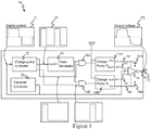
- FIG. 1 shows a block diagram of an ultrasonic transmitter circuit 10 according to an aspect of the present disclosure.
- an ultrasonic transducer 12 is to be driven with a 3-level high voltage square wave.
- the high voltage may be generated on chip by a driving circuit having two charge pumps 14A, 14B that connect to a multilevel inverter 16 that produces an output voltage TX that drives the transducer 12.
- both charge pumps may be turned on simultaneously while supplying the high voltage transmit waveform to the ultrasonic transducer 12 but are otherwise turned off.
- the charge pumps 14A, 14B respectively provide positive and negative high voltage outputs HV+, HV-. Depending on implementation, the charge pumps 14A, 14B may also produce intermediate voltage levels that are used by the multilevel inverter 16.
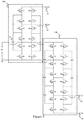
- Figure 5 shows an example implementation of the charge pumps.
- each charge pump 14A, 14B is a symmetric ladder type converter.
- Outputs V3+ and V3- are the positive and negative high voltage outputs, corresponding to HV+ and HV- in Figure 1 .
- Outputs V2+ and V2- may be used as auxiliary outputs, for example, to drive the gates of the high voltage transistors in the multilevel inverter 16 in Figure 1 .
- FIG. 6 shows an example implementation of the multilevel inverter 16.
- the illustrated inverter is implemented with a diode-clamped topology and can produce voltages V3+, 0, or V3- at an output 95.
- the multilevel inverter 16 connects to the charge pumps 14A and 14B through voltages 91, 92, 93, and 94.
- the voltages 91 and 94 are HV+ and HV-, respectively; these are used to drive the transducer 12.
- the voltages 92 and 93 are auxiliary voltages produced by the charge pumps. These are used to drive the gates of the transistors of the multilevel inverter 16. This results in lower power consumption, as the gate drive does not require a full voltage swing from HV+ to HV-.
- the gate drive buffers 96 operate off of the auxiliary voltages. In practice, the control signal to the gate drive buffers 96 needs to be level shifted to the appropriate baseline level. A common approach to implement this is to use AC coupling with a DC level restore.
- a clock generator 18 sets a switching frequency of the charge pump and can be disabled with a digital control signal 19 from the charge pump controller 22 when not used.
- the clock generator 18 may be implemented in the form of some type of hardware-oscillator, with the ability to be turned on or off. If this requires fast start-up time, an RC oscillator may be used. Alternatively, a crystal or MEMS timing device may be used as the clock generator 18.
- a transmit controller 20 generates a digital representation of the 3-level square wave 21, sometimes called a digital transmit waveform.
- the transmit controller 20 may generate a bandpass pulse-width-modulated (BP-PWM) waveform. This type of modulation allows control over the phase and amplitude of the transmit waveform, while needing only a few discrete voltage levels, and thus is compatible with a 3-level square wave.
- BP-PWM pulse-width-modulated
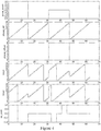
- Figure 3 depicts an example of a BP-PWM unit 30 that may be used as the transmit controller 20 in Figure 1 .
- the BP-PWM unit 30 determines the output voltage level based on the pulse-width setting 31, phase reference 32, and phase offset 33.
- the inputs 31, 32, and 33 may be provided by a higher level controller, for example, a microcontroller or a digital state machine.
- One implementation of a BP-PWM unit 30 uses the algorithm described below to produce the modulated output.
- the algorithm is intended to be representative of the signal processing required to produce the desired waveform and is not the only possible implementation.
- pulse_width is 3 bits
- phase_ref is 4 bits
- phase_offset is 4 bits
- bp_pwm is 2 bits.
- Figure 4 shows the operation of the algorithm.
- the digital transmit waveform 21 feeds into the multilevel inverter 16 and a charge pump controller 22.
- the multilevel inverter 16 is a type of digital to analog converter: it converts an input digital transmit waveform into a high-voltage analog waveform.
- the charge pump controller 22 is responsible for turning on and off the charge pumps 14A, 14B synchronously with the digital transmit waveform 21.
- clock gating elements 24A, 24B and filter capacitors 26A, 26B are also shown in Figure 1 .
- the clock gating elements serve to individually disable the charge pumps.
- the filter capacitors 26A, 26B prevent the charge pump voltage from completely collapsing to zero when the ultrasonic transducer is connected to either the positive or negative charge pump outputs.
- the charge pumps 14A, 14B may be implemented as switched-capacitor DC-DC converters.
- This type of converter uses capacitors to shuffle charge from an input power supply to an output load, e.g., the ultrasonic transducer 12 in this example.
- the basic principle is to charge a capacitor from the input source and then discharge it across the output.
- There are several possible topologies for creating different ratios of output to input voltage For example, several capacitors can be charged from an input source in parallel, and then the capacitors can be connected in series and connected across the output load. This is known as a series-parallel topology and is one method of creating a step-up converter.
- the state of the switches may be controlled by a charge-pump clock, produced by 18 and gated by 24A and 24B. If the clock is high, the even-numbered switches are on and the odd-numbered switches are off. If the clock is low, the opposite is true. The result is that charge is shuffled from the input source Vin to the outputs V2+, V3+, V2-, and V3- by the flying capacitors 90 while the charge pump clocks are active. In this particular topology, V2 will be about twice Vin, and V3 will be 3 times as large as Vin. The converters can be shut-down individually by using the gates 24A and 24B.
- charge is transferred to the output load in discrete packets that occur during the switching transition. For example, a shuffling capacitor has previously been connected across an input voltage source and is now fully charged. The capacitor is then disconnected from the input source and connected across the output load. The charge transfer to the output happens almost instantaneously when the shuffling capacitor is connected to the output load.
- the shuffling capacitor In active operation, the shuffling capacitor periodically switches from the input to the load at a frequency typically in the range of 10 kHz to 100 MHz. While the charge pump is active, the shuffling capacitors are repeatedly charged from the input and discharged to the output.
- the load capacitor will charge while the charge pump is active.
- the load capacitor's final voltage will be determined by the step-up ratio of the charge pump.
- the converter can no longer deliver significant output charge. Further switching action only serves to balance charge on the internal capacitors of the charge pump and does not produce any useful output. Even though the charge pump ceases to produce useful output, there is still energy lost due to the effort required to switch all the internal capacitors. Therefore, it is desirable to place the charge pump into an idle state when the load capacitor reaches a desired output voltage. When the charge pump is placed into an idle state, the load capacitor ceases to charge, and the output voltage becomes constant.
- the capacitive load is an ultrasonic transducer.
- the transducer may be driven with a square wave.
- the transducer driving voltage is periodically switched between the HV+, HV-, and zero levels.
- the peak-to-peak voltage of the transmit waveform (output of the multilevel inverter 16) can be adjusted by changing the amount of time the charge pump is active on each output load switching event. If the active time is longer, the peak-to-peak voltage will be higher.
- the maximum peak-to-peak voltage is generally limited by the peak-to-peak difference between the positive and negative charge pump high voltage outputs.
- the clock generator circuit 18 is turned on for a programmable amount of time, referred to as the active time, at each zero-to-high or zero-to-low edge transition of the digital transmit waveform 21.
- the clock generator 18 is disabled at other times in order to save power by turning off charge pumps 14A, 14B.
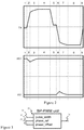
- the positive charge pump (Charge pump P 14A) is turned on at a zero-to-high transition of the digital transmit waveform, and the negative charge pump (Charge pump N 14B) is turned on at a zero-to-low transition. This results in a distinct transmit waveform (output of multilevel inverter 16) with several characteristic phases identified in Figure 2 .
- the transmit waveform ( Figure 2 , top) starts at the zero level.
- there may be a small offset shown as a negative offset in Figure 2 .
- the charge pump outputs ( Figure 2 , bottom) are stable at the voltage level at which they were switched off.
- the multilevel inverter 16 connects the initially discharged load capacitor to the positive high voltage rail (HV+).
- the positive charge pump 14A is enabled for the active time.
- the initial charging will have a fast response up to a certain amplitude that depends on the amount of filtering capacitance 26A at the output of the charge pump 14A.
- the positive charge pump output will decrease due to charge sharing between the capacitive load (e.g., the transducer 12) and filter capacitor 26A.
- phase 3 the positive charge pump 14A is still active, but the initial response due to charge sharing with the filter capacitor 26A has completed.
- the positive charge pump 14A is now charging the load and filter capacitors.
- phase 4 the positive charge pump 14A is in the idle state.
- the output voltage TX stops charging as soon as the positive charge pump 14A goes into the idle state.
- the amplitude of the voltage in phase 4 will increase with the charge pump active time.
- the digital transmit waveform 21 transitions to the 0 level. This causes the multilevel inverter 16 to transition the output to zero. There may be a small offset depending on the topology of the multilevel inverter.
- the charge pump outputs are stable at the voltage level at which they were switched off.
- the multilevel inverter connects the initially discharged load capacitor to the negative high voltage rail (HV-).
- the negative charge pump 14B is enabled for the active time.
- the initial charging will have a fast response up to a certain amplitude that depends on the amount of filtering capacitance 26B at the output of the negative charge pump 14B.
- the negative charge pump output will increase due to charge sharing between the load and filter capacitances.
- the negative charge pump 14B is still active, but the initial response due to charge sharing with the filter capacitor 26B has completed.
- the charge pump is now charging the load and filter capacitors.
- the negative charge pump 14B is in the idle state.
- the output voltage TX stops charging as soon as the negative charge pump 14B goes into the idle state.
- the amplitude of the voltage in phase 8 will increase with the charge pump active time.
- the digital transmit waveform 21 transitions to the 0 level. This causes the multilevel inverter 16 to transition the output to zero. There may be a small offset depending on the topology of the multilevel inverter.
- the system 10 may be designed such that each charge pump is only active when needed to produce the required high voltage output to be applied to transducer 12.
- the positive high voltage charge pump 14A may be active when transducer 12 is driven with positive high voltage HV+.
- the negative high voltage charge pump 14B may be active when transducer 12 is driven with negative high voltage HV-. Otherwise power would be wasted running the charge pumps when it is not necessary to do so.
- the transducer 12 may operate in both a transmit phase and a receive phase.
- the charge pumps 14A, 14B may be turned off during the receive phase to reduce noise. It is noted that aspects of the present disclosure include implementations in which the driving circuit includes a single charge pump, a single clock gating element, and a single filter capacitor.
- aspects of the transmitter circuit 10 are implemented by hardware components, e.g., the charge pump controller 22, transmit controller 20, and clock generator 18. Aspects of the present disclosure are not limited to only such implementations. Aspects of the present disclosure include implementations in which at least some features of the transmitter circuit 10, e.g., some of the functions of the charge pump controller 22, transmit controller 20, or the clock generator 18, or generation of the digital control signal 19 are implemented at least partly in software operating on a programmable processor.
Landscapes
- Engineering & Computer Science (AREA)
- Power Engineering (AREA)
- Mechanical Engineering (AREA)
- Dc-Dc Converters (AREA)
Claims (9)
- Ultraschallsendersystem, umfassend eine integrierte Schaltung (10), einen mehrstufigen Wechselrichter (16) und einen Ultraschallwandler (12), wobei das Ultraschallsendersystem konfiguriert ist, um eine digitale Sendewellenform (21, BP-PWM) zu empfangen und sie auf den Ultraschallwandler (12) anzuwenden, in der Form einer Hochspannungssendewellenform (Tx), wobei die integrierte Schaltung (10) eine oder mehrere Ladepumpen (14A; 14B) umfasst, die an den mehrstufigen Wechselrichter (16) gekoppelt sind, und wobei der mehrstufige Wechselrichter (16) an den Ultraschallwandler (12) gekoppelt ist,
dadurch gekennzeichnet, dass
die eine oder die mehreren Ladepumpen (14A; 14B) konfiguriert sind, um mit einer Zeitplanung zu arbeiten, die auf der digitalen Sendewellenform (21, BP-PWM) basiert, die auf den mehrstufigen Wechselrichter (16) angewandt wird, wobei eine aktive Zeit der einen oder mehreren Ladepumpen (14A; 14B) eine Amplitude der Hochspannungssendewellenform (Tx) bestimmt, die auf den Ultraschallwandler (12) angewandt wird. - System nach Anspruch 1, wobei die Ladepumpen (14A; 14B) konfiguriert sind, um nur aktiv zu sein, wenn es erforderlich ist, die Hochspannungssendewellenform (Tx) auf den Ultraschallwandler (12) anzuwenden.
- System nach Anspruch 1, ferner umfassend einen Taktgenerator (18), der konfiguriert ist, um eine Schaltfrequenz der einen oder mehreren Ladepumpen (14A; 14B) festzulegen.
- System nach Anspruch 3, wobei der Taktgenerator (18) konfiguriert ist, um durch ein digitales Steuersignal (19) deaktiviert zu werden.
- System nach Anspruch 1, wobei die eine oder mehreren Ladepumpen (14A; 14B) als Schaltkondensator-DC-DC-Wandler implementiert sind.
- System nach Anspruch 1, wobei die eine oder mehreren Ladepumpen (14A; 14B) eine erste Ladepumpe (14A; 14B), die konfiguriert ist, um eine positive Antriebsspannungsausgabe zu erzeugen, und eine zweite Ladepumpe (14A; 14B) beinhalten, die konfiguriert ist, um eine negative Antriebsspannungsausgabe zu erzeugen.
- System nach Anspruch 1, ferner umfassend ein oder mehrere Takt-Gating-Elemente (24A; 24B), die konfiguriert sind, um die eine oder mehreren Ladepumpen (14A; 14B) selektiv zu deaktivieren.
- System nach Anspruch 7, ferner umfassend eine Ladepumpensteuerung (22) und einen Taktgenerator (18), die an das eine oder die mehreren Takt-Gating-Elemente (24A; 24B) gekoppelt sind, wobei das eine oder die mehreren Takt-Gating-Elemente (24A; 24B) konfiguriert sind, um die eine oder mehreren Ladepumpen (14A; 14B) als Reaktion auf Signale von der Ladepumpensteuerung (22) und dem Taktgenerator (18) selektiv zu deaktivieren.
- System nach Anspruch 1, wobei die eine oder mehreren Ladepumpen (14A; 14B) unter Verwendung einer symmetrischen Leitertopologie implementiert sind.
Applications Claiming Priority (2)
| Application Number | Priority Date | Filing Date | Title |
|---|---|---|---|
| US201562244574P | 2015-10-21 | 2015-10-21 | |
| PCT/US2016/057972 WO2017070389A1 (en) | 2015-10-21 | 2016-10-20 | Efficient on-chip high-voltage driver circuit for ultrasonic transducer |
Publications (3)
| Publication Number | Publication Date |
|---|---|
| EP3365115A1 EP3365115A1 (de) | 2018-08-29 |
| EP3365115A4 EP3365115A4 (de) | 2019-05-29 |
| EP3365115B1 true EP3365115B1 (de) | 2020-09-30 |
Family
ID=58558099
Family Applications (1)
| Application Number | Title | Priority Date | Filing Date |
|---|---|---|---|
| EP16858243.5A Active EP3365115B1 (de) | 2015-10-21 | 2016-10-20 | Effiziente hochspannungstreiberschaltung auf einem chip für ultraschallwandler |
Country Status (3)
| Country | Link |
|---|---|
| US (1) | US10944320B2 (de) |
| EP (1) | EP3365115B1 (de) |
| WO (1) | WO2017070389A1 (de) |
Families Citing this family (9)
| Publication number | Priority date | Publication date | Assignee | Title |
|---|---|---|---|---|
| EP3472829B1 (de) | 2016-06-17 | 2023-08-16 | InvenSense, Inc. | Piezoelektrische mikrobearbeitete ultraschallwandler mit spannungsentlastungsmerkmalen |
| WO2018095937A1 (en) * | 2016-11-28 | 2018-05-31 | Koninklijke Philips N.V. | Cmut device and imaging method |
| US10784876B1 (en) | 2019-03-14 | 2020-09-22 | Stmicroelectronics Design And Application S.R.O. | Charge pump with load driven clock frequency management |
| US11493979B2 (en) | 2020-02-27 | 2022-11-08 | Fujifilm Sonosite, Inc. | Dynamic power reduction technique for ultrasound systems |
| US12035631B2 (en) * | 2020-06-18 | 2024-07-09 | Cirrus Logic Inc. | Driver circuitry for piezoelectric transducers |
| DE102020120716B4 (de) | 2020-08-05 | 2025-03-13 | Elmos Semiconductor Se | Transformatorlose Ansteuerung eines Ultraschallwandlers mit nur einem externen Energiespeicher |
| GB2601803A (en) * | 2020-12-11 | 2022-06-15 | Univ Leeds Innovations Ltd | Ultrasound transmitter |
| GB202101374D0 (en) * | 2021-02-01 | 2021-03-17 | Sintef Tto As | Object imaging within structures |
| JPWO2022255341A1 (de) * | 2021-06-03 | 2022-12-08 |
Family Cites Families (8)
| Publication number | Priority date | Publication date | Assignee | Title |
|---|---|---|---|---|
| JP3964334B2 (ja) * | 2003-02-06 | 2007-08-22 | ジーイー・メディカル・システムズ・グローバル・テクノロジー・カンパニー・エルエルシー | 超音波診断装置 |
| JP4712519B2 (ja) * | 2005-05-27 | 2011-06-29 | フリースケール セミコンダクター インコーポレイテッド | ハイサイド駆動回路用チャージポンプ回路及びドライバ駆動電圧回路 |
| JP4880275B2 (ja) * | 2005-10-03 | 2012-02-22 | オリンパスメディカルシステムズ株式会社 | 静電容量型超音波振動子装置 |
| US8147409B2 (en) * | 2007-03-29 | 2012-04-03 | Supertex, Inc. | Method and apparatus for transducer excitation in medical ultrasound imaging |
| US9233254B2 (en) * | 2009-02-17 | 2016-01-12 | Boston Scientific Neuromodulation Corporation | Selectable boost converter and charge pump for compliance voltage generation in an implantable stimulator device |
| WO2012055968A1 (en) * | 2010-10-27 | 2012-05-03 | Merus Aps | Audio amplifier using multi-level pulse width modulation |
| US8829980B2 (en) * | 2011-03-21 | 2014-09-09 | Analog Devices, Inc. | Phased-array charge pump supply |
| ITUB20159673A1 (it) * | 2015-12-21 | 2017-06-21 | St Microelectronics Srl | Amplificatore a guadagno programmabile, dispositivo e procedimento corrispondenti |
-
2016
- 2016-10-20 EP EP16858243.5A patent/EP3365115B1/de active Active
- 2016-10-20 WO PCT/US2016/057972 patent/WO2017070389A1/en not_active Ceased
-
2018
- 2018-04-20 US US15/958,415 patent/US10944320B2/en active Active
Non-Patent Citations (1)
| Title |
|---|
| None * |
Also Published As
| Publication number | Publication date |
|---|---|
| WO2017070389A1 (en) | 2017-04-27 |
| EP3365115A4 (de) | 2019-05-29 |
| EP3365115A1 (de) | 2018-08-29 |
| US10944320B2 (en) | 2021-03-09 |
| US20180248477A1 (en) | 2018-08-30 |
Similar Documents
| Publication | Publication Date | Title |
|---|---|---|
| EP3365115B1 (de) | Effiziente hochspannungstreiberschaltung auf einem chip für ultraschallwandler | |
| US10651731B1 (en) | Zero voltage switching of interleaved switched-capacitor converters | |
| TWI339008B (en) | Class-d amplifier and multi-level output signal generated method thereof | |
| US7180759B2 (en) | Push-pull inverter with snubber energy recovery | |
| US12323055B2 (en) | Driver circuitry and operation | |
| US10250145B2 (en) | Device for avoiding hard switching in resonant converter and related method | |
| US20140300188A1 (en) | Capacitive level shifter devices, methods and systems | |
| US11277129B2 (en) | Driver circuitry and operation | |
| US11684950B2 (en) | Driver circuitry and operation | |
| US20250260317A1 (en) | Driver circuitry and operation | |
| CN113972836B (zh) | 一种三电平升压变换器及控制方法 | |
| US9673735B2 (en) | Power converter | |
| KR20170084017A (ko) | 클래스 d 전력 드라이버 주변장치 | |
| CN105193450B (zh) | 一种超声成像系统的高压电源控制方法 | |
| JP6825460B2 (ja) | 電源装置 | |
| US20070103138A1 (en) | Dc-dc converter and power supply device | |
| CN117242688A (zh) | 驱动器电路和操作 | |
| Gruber et al. | A Fully Integrated Bipolar 1.8 Vpp-to-41Vpp 450kHz Switched-Capacitor MEMS-Driver with a Power Reduction Factor of 16.3 | |
| US7298100B2 (en) | Driving apparatus for vibration type actuator and driving method for vibration type actuator | |
| CN116097559A (zh) | 驱动器电路和操作 | |
| US20220368325A1 (en) | Driver circuitry and operation | |
| EP2434644A1 (de) | Hochspannungs-Floating-Gate-Treibertopologie für sehr hohe Schaltfrequenzen | |
| US20260101672A1 (en) | Device and methods for an integrated haptic driver | |
| US5682302A (en) | Adaptable power converter applying digitized-wave-generation for integrated circuit implementation | |
| US20140042872A1 (en) | Polarity switching circuit |
Legal Events
| Date | Code | Title | Description |
|---|---|---|---|
| STAA | Information on the status of an ep patent application or granted ep patent |
Free format text: STATUS: THE INTERNATIONAL PUBLICATION HAS BEEN MADE |
|
| PUAI | Public reference made under article 153(3) epc to a published international application that has entered the european phase |
Free format text: ORIGINAL CODE: 0009012 |
|
| STAA | Information on the status of an ep patent application or granted ep patent |
Free format text: STATUS: REQUEST FOR EXAMINATION WAS MADE |
|
| 17P | Request for examination filed |
Effective date: 20180412 |
|
| AK | Designated contracting states |
Kind code of ref document: A1 Designated state(s): AL AT BE BG CH CY CZ DE DK EE ES FI FR GB GR HR HU IE IS IT LI LT LU LV MC MK MT NL NO PL PT RO RS SE SI SK SM TR |
|
| AX | Request for extension of the european patent |
Extension state: BA ME |
|
| DAV | Request for validation of the european patent (deleted) | ||
| DAX | Request for extension of the european patent (deleted) | ||
| REG | Reference to a national code |
Ref country code: DE Ref legal event code: R079 Ref document number: 602016045167 Country of ref document: DE Free format text: PREVIOUS MAIN CLASS: B06B0001020000 Ipc: H02M0003070000 |
|
| A4 | Supplementary search report drawn up and despatched |
Effective date: 20190429 |
|
| RIC1 | Information provided on ipc code assigned before grant |
Ipc: H02M 1/08 20060101ALI20190423BHEP Ipc: H02M 1/36 20070101ALI20190423BHEP Ipc: B06B 1/02 20060101ALI20190423BHEP Ipc: H02M 1/00 20060101ALI20190423BHEP Ipc: H02M 7/483 20070101ALI20190423BHEP Ipc: H02M 3/07 20060101AFI20190423BHEP |
|
| RIC1 | Information provided on ipc code assigned before grant |
Ipc: H02M 1/08 20060101ALI20190521BHEP Ipc: B06B 1/02 20060101ALI20190521BHEP Ipc: H02M 7/483 20070101ALI20190521BHEP Ipc: H02M 3/07 20060101AFI20190521BHEP Ipc: H02M 1/36 20070101ALI20190521BHEP Ipc: H02M 1/00 20060101ALI20190521BHEP |
|
| GRAP | Despatch of communication of intention to grant a patent |
Free format text: ORIGINAL CODE: EPIDOSNIGR1 |
|
| STAA | Information on the status of an ep patent application or granted ep patent |
Free format text: STATUS: GRANT OF PATENT IS INTENDED |
|
| INTG | Intention to grant announced |
Effective date: 20200520 |
|
| GRAS | Grant fee paid |
Free format text: ORIGINAL CODE: EPIDOSNIGR3 |
|
| GRAA | (expected) grant |
Free format text: ORIGINAL CODE: 0009210 |
|
| STAA | Information on the status of an ep patent application or granted ep patent |
Free format text: STATUS: THE PATENT HAS BEEN GRANTED |
|
| AK | Designated contracting states |
Kind code of ref document: B1 Designated state(s): AL AT BE BG CH CY CZ DE DK EE ES FI FR GB GR HR HU IE IS IT LI LT LU LV MC MK MT NL NO PL PT RO RS SE SI SK SM TR |
|
| REG | Reference to a national code |
Ref country code: CH Ref legal event code: EP Ref country code: GB Ref legal event code: FG4D |
|
| REG | Reference to a national code |
Ref country code: DE Ref legal event code: R096 Ref document number: 602016045167 Country of ref document: DE Ref country code: AT Ref legal event code: REF Ref document number: 1319826 Country of ref document: AT Kind code of ref document: T Effective date: 20201015 |
|
| REG | Reference to a national code |
Ref country code: IE Ref legal event code: FG4D |
|
| PG25 | Lapsed in a contracting state [announced via postgrant information from national office to epo] |
Ref country code: GR Free format text: LAPSE BECAUSE OF FAILURE TO SUBMIT A TRANSLATION OF THE DESCRIPTION OR TO PAY THE FEE WITHIN THE PRESCRIBED TIME-LIMIT Effective date: 20201231 Ref country code: NO Free format text: LAPSE BECAUSE OF FAILURE TO SUBMIT A TRANSLATION OF THE DESCRIPTION OR TO PAY THE FEE WITHIN THE PRESCRIBED TIME-LIMIT Effective date: 20201230 Ref country code: BG Free format text: LAPSE BECAUSE OF FAILURE TO SUBMIT A TRANSLATION OF THE DESCRIPTION OR TO PAY THE FEE WITHIN THE PRESCRIBED TIME-LIMIT Effective date: 20201230 Ref country code: HR Free format text: LAPSE BECAUSE OF FAILURE TO SUBMIT A TRANSLATION OF THE DESCRIPTION OR TO PAY THE FEE WITHIN THE PRESCRIBED TIME-LIMIT Effective date: 20200930 Ref country code: SE Free format text: LAPSE BECAUSE OF FAILURE TO SUBMIT A TRANSLATION OF THE DESCRIPTION OR TO PAY THE FEE WITHIN THE PRESCRIBED TIME-LIMIT Effective date: 20200930 Ref country code: FI Free format text: LAPSE BECAUSE OF FAILURE TO SUBMIT A TRANSLATION OF THE DESCRIPTION OR TO PAY THE FEE WITHIN THE PRESCRIBED TIME-LIMIT Effective date: 20200930 |
|
| REG | Reference to a national code |
Ref country code: AT Ref legal event code: MK05 Ref document number: 1319826 Country of ref document: AT Kind code of ref document: T Effective date: 20200930 |
|
| PG25 | Lapsed in a contracting state [announced via postgrant information from national office to epo] |
Ref country code: RS Free format text: LAPSE BECAUSE OF FAILURE TO SUBMIT A TRANSLATION OF THE DESCRIPTION OR TO PAY THE FEE WITHIN THE PRESCRIBED TIME-LIMIT Effective date: 20200930 Ref country code: LV Free format text: LAPSE BECAUSE OF FAILURE TO SUBMIT A TRANSLATION OF THE DESCRIPTION OR TO PAY THE FEE WITHIN THE PRESCRIBED TIME-LIMIT Effective date: 20200930 |
|
| REG | Reference to a national code |
Ref country code: NL Ref legal event code: MP Effective date: 20200930 |
|
| REG | Reference to a national code |
Ref country code: LT Ref legal event code: MG4D |
|
| PG25 | Lapsed in a contracting state [announced via postgrant information from national office to epo] |
Ref country code: CZ Free format text: LAPSE BECAUSE OF FAILURE TO SUBMIT A TRANSLATION OF THE DESCRIPTION OR TO PAY THE FEE WITHIN THE PRESCRIBED TIME-LIMIT Effective date: 20200930 Ref country code: PT Free format text: LAPSE BECAUSE OF FAILURE TO SUBMIT A TRANSLATION OF THE DESCRIPTION OR TO PAY THE FEE WITHIN THE PRESCRIBED TIME-LIMIT Effective date: 20210201 Ref country code: RO Free format text: LAPSE BECAUSE OF FAILURE TO SUBMIT A TRANSLATION OF THE DESCRIPTION OR TO PAY THE FEE WITHIN THE PRESCRIBED TIME-LIMIT Effective date: 20200930 Ref country code: LT Free format text: LAPSE BECAUSE OF FAILURE TO SUBMIT A TRANSLATION OF THE DESCRIPTION OR TO PAY THE FEE WITHIN THE PRESCRIBED TIME-LIMIT Effective date: 20200930 Ref country code: SM Free format text: LAPSE BECAUSE OF FAILURE TO SUBMIT A TRANSLATION OF THE DESCRIPTION OR TO PAY THE FEE WITHIN THE PRESCRIBED TIME-LIMIT Effective date: 20200930 Ref country code: EE Free format text: LAPSE BECAUSE OF FAILURE TO SUBMIT A TRANSLATION OF THE DESCRIPTION OR TO PAY THE FEE WITHIN THE PRESCRIBED TIME-LIMIT Effective date: 20200930 |
|
| PG25 | Lapsed in a contracting state [announced via postgrant information from national office to epo] |
Ref country code: PL Free format text: LAPSE BECAUSE OF FAILURE TO SUBMIT A TRANSLATION OF THE DESCRIPTION OR TO PAY THE FEE WITHIN THE PRESCRIBED TIME-LIMIT Effective date: 20200930 Ref country code: IS Free format text: LAPSE BECAUSE OF FAILURE TO SUBMIT A TRANSLATION OF THE DESCRIPTION OR TO PAY THE FEE WITHIN THE PRESCRIBED TIME-LIMIT Effective date: 20210130 Ref country code: ES Free format text: LAPSE BECAUSE OF FAILURE TO SUBMIT A TRANSLATION OF THE DESCRIPTION OR TO PAY THE FEE WITHIN THE PRESCRIBED TIME-LIMIT Effective date: 20200930 Ref country code: AT Free format text: LAPSE BECAUSE OF FAILURE TO SUBMIT A TRANSLATION OF THE DESCRIPTION OR TO PAY THE FEE WITHIN THE PRESCRIBED TIME-LIMIT Effective date: 20200930 Ref country code: AL Free format text: LAPSE BECAUSE OF FAILURE TO SUBMIT A TRANSLATION OF THE DESCRIPTION OR TO PAY THE FEE WITHIN THE PRESCRIBED TIME-LIMIT Effective date: 20200930 |
|
| REG | Reference to a national code |
Ref country code: CH Ref legal event code: PL |
|
| PG25 | Lapsed in a contracting state [announced via postgrant information from national office to epo] |
Ref country code: SK Free format text: LAPSE BECAUSE OF FAILURE TO SUBMIT A TRANSLATION OF THE DESCRIPTION OR TO PAY THE FEE WITHIN THE PRESCRIBED TIME-LIMIT Effective date: 20200930 Ref country code: MC Free format text: LAPSE BECAUSE OF FAILURE TO SUBMIT A TRANSLATION OF THE DESCRIPTION OR TO PAY THE FEE WITHIN THE PRESCRIBED TIME-LIMIT Effective date: 20200930 Ref country code: NL Free format text: LAPSE BECAUSE OF FAILURE TO SUBMIT A TRANSLATION OF THE DESCRIPTION OR TO PAY THE FEE WITHIN THE PRESCRIBED TIME-LIMIT Effective date: 20200930 Ref country code: LU Free format text: LAPSE BECAUSE OF NON-PAYMENT OF DUE FEES Effective date: 20201020 |
|
| REG | Reference to a national code |
Ref country code: DE Ref legal event code: R097 Ref document number: 602016045167 Country of ref document: DE |
|
| REG | Reference to a national code |
Ref country code: BE Ref legal event code: MM Effective date: 20201031 |
|
| PLBE | No opposition filed within time limit |
Free format text: ORIGINAL CODE: 0009261 |
|
| STAA | Information on the status of an ep patent application or granted ep patent |
Free format text: STATUS: NO OPPOSITION FILED WITHIN TIME LIMIT |
|
| GBPC | Gb: european patent ceased through non-payment of renewal fee |
Effective date: 20201230 |
|
| PG25 | Lapsed in a contracting state [announced via postgrant information from national office to epo] |
Ref country code: BE Free format text: LAPSE BECAUSE OF NON-PAYMENT OF DUE FEES Effective date: 20201031 Ref country code: DK Free format text: LAPSE BECAUSE OF FAILURE TO SUBMIT A TRANSLATION OF THE DESCRIPTION OR TO PAY THE FEE WITHIN THE PRESCRIBED TIME-LIMIT Effective date: 20200930 Ref country code: CH Free format text: LAPSE BECAUSE OF NON-PAYMENT OF DUE FEES Effective date: 20201031 Ref country code: LI Free format text: LAPSE BECAUSE OF NON-PAYMENT OF DUE FEES Effective date: 20201031 |
|
| 26N | No opposition filed |
Effective date: 20210701 |
|
| PG25 | Lapsed in a contracting state [announced via postgrant information from national office to epo] |
Ref country code: FR Free format text: LAPSE BECAUSE OF NON-PAYMENT OF DUE FEES Effective date: 20201130 Ref country code: IT Free format text: LAPSE BECAUSE OF FAILURE TO SUBMIT A TRANSLATION OF THE DESCRIPTION OR TO PAY THE FEE WITHIN THE PRESCRIBED TIME-LIMIT Effective date: 20200930 Ref country code: IE Free format text: LAPSE BECAUSE OF NON-PAYMENT OF DUE FEES Effective date: 20201020 |
|
| PG25 | Lapsed in a contracting state [announced via postgrant information from national office to epo] |
Ref country code: GB Free format text: LAPSE BECAUSE OF NON-PAYMENT OF DUE FEES Effective date: 20201230 Ref country code: SI Free format text: LAPSE BECAUSE OF FAILURE TO SUBMIT A TRANSLATION OF THE DESCRIPTION OR TO PAY THE FEE WITHIN THE PRESCRIBED TIME-LIMIT Effective date: 20200930 |
|
| PG25 | Lapsed in a contracting state [announced via postgrant information from national office to epo] |
Ref country code: IS Free format text: LAPSE BECAUSE OF FAILURE TO SUBMIT A TRANSLATION OF THE DESCRIPTION OR TO PAY THE FEE WITHIN THE PRESCRIBED TIME-LIMIT Effective date: 20210130 Ref country code: TR Free format text: LAPSE BECAUSE OF FAILURE TO SUBMIT A TRANSLATION OF THE DESCRIPTION OR TO PAY THE FEE WITHIN THE PRESCRIBED TIME-LIMIT Effective date: 20200930 Ref country code: MT Free format text: LAPSE BECAUSE OF FAILURE TO SUBMIT A TRANSLATION OF THE DESCRIPTION OR TO PAY THE FEE WITHIN THE PRESCRIBED TIME-LIMIT Effective date: 20200930 Ref country code: CY Free format text: LAPSE BECAUSE OF FAILURE TO SUBMIT A TRANSLATION OF THE DESCRIPTION OR TO PAY THE FEE WITHIN THE PRESCRIBED TIME-LIMIT Effective date: 20200930 |
|
| REG | Reference to a national code |
Ref country code: DE Ref legal event code: R081 Ref document number: 602016045167 Country of ref document: DE Owner name: INVENSENSE, INC., SAN JOSE, US Free format text: FORMER OWNER: CHIRP MICROSYSTEMS, INC., BERKELEY, CA, US |
|
| PG25 | Lapsed in a contracting state [announced via postgrant information from national office to epo] |
Ref country code: MK Free format text: LAPSE BECAUSE OF FAILURE TO SUBMIT A TRANSLATION OF THE DESCRIPTION OR TO PAY THE FEE WITHIN THE PRESCRIBED TIME-LIMIT Effective date: 20200930 |
|
| P01 | Opt-out of the competence of the unified patent court (upc) registered |
Effective date: 20230524 |
|
| PGFP | Annual fee paid to national office [announced via postgrant information from national office to epo] |
Ref country code: DE Payment date: 20250902 Year of fee payment: 10 |