EP3365784B1 - Agencement de circuits et procédé de surveillance d'un microcontrôleur à base d'une tension de surveillance - Google Patents
Agencement de circuits et procédé de surveillance d'un microcontrôleur à base d'une tension de surveillance Download PDFInfo
- Publication number
- EP3365784B1 EP3365784B1 EP16787765.3A EP16787765A EP3365784B1 EP 3365784 B1 EP3365784 B1 EP 3365784B1 EP 16787765 A EP16787765 A EP 16787765A EP 3365784 B1 EP3365784 B1 EP 3365784B1
- Authority
- EP
- European Patent Office
- Prior art keywords
- capacitor
- microcontroller
- voltage
- time
- monitoring
- Prior art date
- Legal status (The legal status is an assumption and is not a legal conclusion. Google has not performed a legal analysis and makes no representation as to the accuracy of the status listed.)
- Active
Links
Images

Classifications
-
- G—PHYSICS
- G06—COMPUTING OR CALCULATING; COUNTING
- G06F—ELECTRIC DIGITAL DATA PROCESSING
- G06F11/00—Error detection; Error correction; Monitoring
- G06F11/07—Responding to the occurrence of a fault, e.g. fault tolerance
- G06F11/0703—Error or fault processing not based on redundancy, i.e. by taking additional measures to deal with the error or fault not making use of redundancy in operation, in hardware, or in data representation
- G06F11/0751—Error or fault detection not based on redundancy
- G06F11/0754—Error or fault detection not based on redundancy by exceeding limits
-
- G—PHYSICS
- G06—COMPUTING OR CALCULATING; COUNTING
- G06F—ELECTRIC DIGITAL DATA PROCESSING
- G06F11/00—Error detection; Error correction; Monitoring
- G06F11/07—Responding to the occurrence of a fault, e.g. fault tolerance
- G06F11/0703—Error or fault processing not based on redundancy, i.e. by taking additional measures to deal with the error or fault not making use of redundancy in operation, in hardware, or in data representation
- G06F11/0706—Error or fault processing not based on redundancy, i.e. by taking additional measures to deal with the error or fault not making use of redundancy in operation, in hardware, or in data representation the processing taking place on a specific hardware platform or in a specific software environment
- G06F11/0736—Error or fault processing not based on redundancy, i.e. by taking additional measures to deal with the error or fault not making use of redundancy in operation, in hardware, or in data representation the processing taking place on a specific hardware platform or in a specific software environment in functional embedded systems, i.e. in a data processing system designed as a combination of hardware and software dedicated to performing a certain function
- G06F11/0739—Error or fault processing not based on redundancy, i.e. by taking additional measures to deal with the error or fault not making use of redundancy in operation, in hardware, or in data representation the processing taking place on a specific hardware platform or in a specific software environment in functional embedded systems, i.e. in a data processing system designed as a combination of hardware and software dedicated to performing a certain function in a data processing system embedded in automotive or aircraft systems
-
- G—PHYSICS
- G01—MEASURING; TESTING
- G01R—MEASURING ELECTRIC VARIABLES; MEASURING MAGNETIC VARIABLES
- G01R31/00—Arrangements for testing electric properties; Arrangements for locating electric faults; Arrangements for electrical testing characterised by what is being tested not provided for elsewhere
- G01R31/28—Testing of electronic circuits, e.g. by signal tracer
- G01R31/317—Testing of digital circuits
- G01R31/31712—Input or output aspects
-
- G—PHYSICS
- G05—CONTROLLING; REGULATING
- G05B—CONTROL OR REGULATING SYSTEMS IN GENERAL; FUNCTIONAL ELEMENTS OF SUCH SYSTEMS; MONITORING OR TESTING ARRANGEMENTS FOR SUCH SYSTEMS OR ELEMENTS
- G05B23/00—Testing or monitoring of control systems or parts thereof
- G05B23/02—Electric testing or monitoring
- G05B23/0205—Electric testing or monitoring by means of a monitoring system capable of detecting and responding to faults
- G05B23/0218—Electric testing or monitoring by means of a monitoring system capable of detecting and responding to faults characterised by the fault detection method dealing with either existing or incipient faults
- G05B23/0243—Electric testing or monitoring by means of a monitoring system capable of detecting and responding to faults characterised by the fault detection method dealing with either existing or incipient faults model based detection method, e.g. first-principles knowledge model
- G05B23/0254—Electric testing or monitoring by means of a monitoring system capable of detecting and responding to faults characterised by the fault detection method dealing with either existing or incipient faults model based detection method, e.g. first-principles knowledge model based on a quantitative model, e.g. mathematical relationships between inputs and outputs; functions: observer, Kalman filter, residual calculation, Neural Networks
-
- G—PHYSICS
- G06—COMPUTING OR CALCULATING; COUNTING
- G06F—ELECTRIC DIGITAL DATA PROCESSING
- G06F11/00—Error detection; Error correction; Monitoring
- G06F11/07—Responding to the occurrence of a fault, e.g. fault tolerance
- G06F11/0703—Error or fault processing not based on redundancy, i.e. by taking additional measures to deal with the error or fault not making use of redundancy in operation, in hardware, or in data representation
- G06F11/0751—Error or fault detection not based on redundancy
- G06F11/0754—Error or fault detection not based on redundancy by exceeding limits
- G06F11/0757—Error or fault detection not based on redundancy by exceeding limits by exceeding a time limit, i.e. time-out, e.g. watchdogs
Definitions
- the invention relates to a circuit arrangement, and more particularly relates to a digital watchdog or watchdog (WD) circuit for monitoring the timing behavior or timing behavior of a microcontroller. Furthermore, the invention relates to a method for monitoring a microcontroller based on a guard voltage generated by a guard circuit.
- WD digital watchdog or watchdog
- Watchdog or watchdog (WD) circuits for the timing of a microcontroller in the form of digital circuits and methods are known in the art.
- Also known per se are fixed static reference voltages at an input terminal or PIN of an analog-to-digital converter (ADC) to a microcontroller, which is to ensure the correct functioning of the ADC.
- ADC analog-to-digital converter
- DE 10 2013 226429 A1 discloses a circuit arrangement for monitoring the timing behavior of a microcontroller including a microcontroller arranged to drive at least one monitor voltage generating section for generating at least one monitor voltage in a timely manner, and the at least one monitor voltage generating section arranged to generate the detectable monitor voltage detected, lying within a predetermined voltage tolerance range monitoring voltage indicating a healthy state of the microcontroller, and a detected, lying outside the predetermined voltage tolerance range monitoring voltage indicates a faulty state of the microcontroller.
- WO 2009/040216 A2 describes a vehicle control unit with a supply voltage monitored microcontroller, wherein the voltage to be monitored is detected by the microcontroller by means of A / D converter, read and checked for correctness.
- the invention is therefore based on an object to provide for a one-processor system with a microcontroller, a circuit arrangement and a method for its monitoring, with the or the analog (ADC) inputs of the microcontroller for correct operation and possibly at the same time even the microcontroller even be checked for correct internal timing.
- ADC analog
- this object is achieved by a watchdog circuit arrangement having the features of patent claim 1 and by a method for monitoring a microcontroller based on a guard voltage having the features of claim 9.
- Advantageous developments of the invention are the subject of the appended subclaims.
- the invention is based on the general idea of providing a cost-effective and at the same time simple circuit arrangement which allows a simple but effective checking of the timing of a microcontroller.
- the two requirements for a verification of the function of an analog-to-digital converter and for a correct timing of the microcontroller (.mu.C) are combined.
- the circuit requires in the embodiments described below, only five to eight low-cost standard components.
- a necessary independent reference voltage can optionally also be provided by another circuit part, so that no additional components are required for this purpose.
- a highly stable reference voltage the value of which is well known, and known tolerances of used components defining an allowable range for a voltage detection value
- first completely discharges a capacitor and then, beginning at a particular time, along a charge curve passing through Timer is determined, reloaded. From this particular point in time the charge time up to a certain voltage, in the present case the monitoring voltage to be detected, which the microcontroller will read in after this time, is exactly known.
- the charging time is specified exactly by the microcontroller and is thus an absolute measure of the voltage to be read back. Due to the strict dependence of the charging time and the value of the monitoring voltage, the absolute charging time is included directly in the result.
- this absolute charging time changes due to, for example, a deviating timing or a malfunction within the microcontroller
- the monitoring voltage changes proportionally. If the monitoring voltage thereby leaves the tolerance band determined by the component tolerances, these errors can be clearly recognized in the microcontroller and the overall system can be brought into a safety-critical operating state.
- the watchdog circuitry includes a microcontroller arranged to drive at least one watchdog voltage generating section for timely generating at least one monitor voltage and to detect and read the monitor voltage then generated at a predetermined sampling instant, and the at least one watchdog voltage generating section arranged thereon detectable at a predetermined sampling time by sampling by the microcontroller detectable monitoring voltage, wherein a detected at the sampling time, lying within a predetermined voltage tolerance range monitoring voltage indicating a healthy state of the microcontroller, and detected at the predetermined time, lying outside the predetermined voltage tolerance range monitoring voltage a faulty State of the microcontroller indicates.
- the watchdog voltage generating section has at least one capacitor, at which the monitoring voltage is provided. Since the voltage curve of a charging curve on a capacitor is likewise known in the case of components whose parameters are known, a simple voltage sampling can advantageously be represented.
- the Wambaterschreibser Wegungsabites has at least one transistor which is connected in parallel with the capacitor and in response to a logic state at an output of the microcontroller by the microcontroller timed switchable, wherein during a state of logic 0 of the output, the transistor is turned off and the capacitor is definable loadable, and during a state of logic 1 of the output, the transistor is turned on and the capacitor is defined dischargeable.
- a transistor as a switching element in the underlying voltage and / or power range is an advantageously cost-effective way to control the charging and / or the discharge of a capacitor.
- the underlying parameters and waveforms are exactly determined and predictable.
- a first guard voltage generating section in which a first first resistor is connected in series with a first capacitor and at a first of its ends is at a reference voltage, and at a second of its ends is connected to a first terminal of the first capacitor; a supply resistor is provided which is connected to a supply voltage at a first end thereof and connected at a second end thereof to the cathode side of a diode which provides the reference voltage between the first end of the first first resistor and a second terminal of the first capacitor; and a first transistor having a first terminal connected to the first terminal of the first capacitor and a first analog converter input of the microcontroller, a second terminal connected to a first output of the microcontroller, and a third terminal connected to the second terminal of the microcontroller first capacitor, on the anode side with the diode and a Ground potential is connected; and a second guard voltage generating section is provided in which a second first resistor is connected in series with a second capacitor and at a first of its ends is
- the first monitor voltage generating section and the second monitor voltage generating section are driven and sampled such that one of the monitor voltages on one of the capacitors is detected at a first predetermined time and read by the microcontroller, and another of the monitor voltages on another of the monitor voltages Capacitors detected at a second predetermined time and read by the microcontroller.
- a further detection of individual errors on the watchdog circuit is thus possible, for example if it has micro-controllers sporadic clock misfires or a defect of the control port DO_1 for the discharge transistor T1. The defect would cause C1 to discharge, which would not be detected if the ⁇ C would then continue from this state. C2 would continue to charge due to the dropout of the ⁇ C and thus fall outside the tolerance window, so the error would be recognizable by the second channel.
- the time constant of the timer determined by the first first resistor and the first capacitor and the time constant of the timer determined by the second first resistor and the second capacitor differ from each other.
- so-called common-mode disturbances can be distinguished better.
- samples of the charging curve of the capacitor are cyclically repeated at defined sampling times. Cyclic sampling ensures continuous monitoring of the microcontroller during its operation.
- the microcontroller is arranged to block the transistor until the capacitor is fully charged, thereafter to detect the absolute value of the reference voltage, and to calibrate at least one analog to digital converter channel of the microcontroller based on the detected value of the reference voltage.
- the detection accuracy of the analog-to-digital converter can be further increased.
- the electronic switch is designed as a transistor. More preferably, the electronic switch is formed integrated into the microcontroller. Alternatively preferably, the electronic switch is provided lying outside of the microcontroller and connected thereto.
- a method for monitoring a microcontroller on the basis of a voltage for monitoring the timing behavior of a microcontroller, which is generated in a previously described guard circuit comprising the steps of: driving at least one guard voltage generating section for generating at least one monitoring voltage in a timely manner wherein the driving includes a defined discharging of a capacitor and then, starting at a predetermined time, defined charging of the capacitor along a charging curve; and detecting and reading in the charging voltage of the capacitor generated at a predetermined sampling timing as the monitor voltage, wherein a monitor voltage detected within the sampling voltage time range indicates a healthy state of the microcontroller, and a detected value outside the predetermined voltage tolerance range detected at the predetermined timing Monitoring voltage indicates a faulty state of the microcontroller.
- a transistor is disabled and the capacitor is loadable, and becomes definable during a state of logic 1 of the output, the transistor is turned on and the capacitor is defined to be dischargeable.
- a first guard voltage generating section and a second guard voltage generating section are driven and scanned in such a phase that one of the monitor voltages on one of the capacitors is detected at a first predetermined time and read by the microcontroller, and another of the monitor voltages on another of the capacitors is second predetermined Time is detected and read by the microcontroller.
- a time constant of an RC timer of a first guard voltage generating section and a time constant of an RC timer of a second guard voltage generating section are different from each other.
- samples of the charging curve of the capacitor are cyclically repeated at defined sampling times.
- the transistor is turned off until the capacitor is fully charged, thereafter the absolute value of the reference voltage is detected, and at least one analog-to-digital converter channel of the microcontroller is calibrated based on the detected value of the reference voltage.
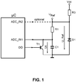
- Fig. 1 shows a simplified, fragmentary schematic representation of a guard circuit for monitoring the timing behavior or timing behavior of a microcontroller.
- the in Fig. 1 Microcontroller ⁇ C shown on the left is a control device which can be used in, for example, systems, electronic control units (ECU) and the like for vehicles, in particular commercial vehicles, and is well known as such.
- the microcontroller .mu.C in addition to commonly available inputs and outputs or ports at least a first analog-to-digital converter input ADC_IN1 and a digital output or digital output DO. It is understood that further inputs, for example a second analog-to-digital converter input ADC_IN2, can be provided.
- a guard voltage generating section which at least with the aforementioned first analog-to-digital converter input ADC_IN1 and connected to the output DO and at least one transistor T1, a capacitor C1, a resistor R1, a diode D1 and a resistor R3 includes.
- a connection of the guard voltage generating section with the second analog-to-digital converter input ADC_IN2 may be optional, as will be described later.
- a first terminal of the transistor T1 for example the drain or collector terminal, is connected to the first input ADC_IN1 of the microcontroller ⁇ C, and a second terminal of the transistor T1, for example the gate or base terminal, is connected to the digital output DO. Further, the first terminal of the transistor T1 is connected to a second end of the resistor R1 and a first terminal of the capacitor C1. A second end of the resistor R1 is connected to a reference voltage U Ref , which is provided via the diode D1, for example a suitable zener diode.
- the diode D1 is parallel to the series circuit of the resistor R1 and the capacitor C1 and is of the resistor R3, for example, from a supply voltage Vcc, for example 5V an electronic control unit (ECU) in which both the microcontroller microcontroller and the guard voltage generating section arranged or are integrated, supplied.
- Vcc supply voltage
- ECU electronice control unit
- a third terminal of the transistor T1 (source or emitter), a second terminal of the capacitor C1 and the anode side of the diode D1 are connected to a common node at a ground potential.
- the transistor T1 which forms in this configuration a discharge transistor for the capacitor C1 is parallel to the capacitor C1, and the series circuit of the resistor R1 and the capacitor C1, which in this configuration is an RC element R1 / C1, parallel to the diode D1.
- the transistor T1 described above which operates in the described configuration as a discharge transistor for the capacitor C1, can also already be integrated in the microcontroller ⁇ C in a modification of the present exemplary embodiment and as a variant of a microcontroller port.
- the capacitor C1 may be directly connected to the corresponding input and output ports of the microcontroller ⁇ C.
- the voltage (U Ref ) across the diode, which is supplied via the resistor R3, for example, to the supply voltage Vcc, is preferably a high-precision reference voltage whose value is precisely known and which is independent of other supply voltages.
- the dimensioning or the values of the resistor R1, the capacitor C1 and the transistor T1 are precisely known, as well as tolerances of these respective components. Thus, the charging time constant is known. Tolerance limits, which are yet to be described and in this embodiment with U min (lower tolerance limit) and U max (upper tolerance limit) are designated and as such represent a tolerance band, can be expertly calculated.
- the microcontroller ⁇ C is arranged to drive the transistor T1 via the digital output DO, i. to block or switch through. Therefore, by blocking the transistor T1, the microcontroller .mu.C can fully charge the capacitor C1 at an arbitrary time, and thereafter, for example, at a predetermined time t0, by enabling, i. permeable switching, the transistor T1 discharged again. In other words, the capacitor C1 can recharge from the predetermined time t0.
- U U Ref * (1-exp (-t / R * C)
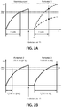
- Fig. 2A and Fig.2B Sectionally show typical signal waveforms in the form of voltage waveforms at different operating states in the watchdog circuitry according to Fig. 1 ,
- FIGS. 2A and 2B the capacitor voltage Uc applied to the capacitor C1 and the time along the abscissa are plotted along the ordinate.
- FIGS. 2A and 2B show FIGS. 2A and 2B so that a charging voltage curve of the capacitor C1 over time.
- FIGS. 2A and 2B Charging curves shown in detail from cyclic repetitions of charging and discharging processes show in detail the beginning of a charging of the capacitor C1 at a time in FIGS. 2A and 2B for example, in the origin (0, 0) of the coordinate system.
- the monitoring voltage Uc increases according to the above equation.
- the monitoring voltage Uc reached is then sampled and read in or read back by the microcontroller .mu.C at the sampling or sampling point then reached.
- Fig. 2A refers in its right-hand part to an error case 1, in which, although the charging time t_Lade is correct, but, for example, values and / or parameters of the timer R1 / C1 are outside allowable tolerances.
- the error case 1 is detected.
- Fig. 2B in its left-hand part refers to an error case 2 in which the charging time t_load is too short, and in its right-hand part to an error case 3 in which the charging time t_load is too long. Due to the too short charging time until the sampling time, the monitor voltage Uc does not reach the tolerance band, and the error case 2 is detected. Due to the too long charging time to the sampling time, the monitoring voltage Uc exceeds the tolerance band, and the error case 3 is detected.
- the time how long after the sampling point the capacitor C1 can or should continue to charge, and the time for which the capacitor C1 then remains discharged, can be chosen arbitrarily and does not enter the voltage measurement.
- the microcontroller ⁇ C discharges the capacitor C1 completely by switching on the transistor T1 at a selectable instant.
- the microcontroller ⁇ C begins by blocking the transistor T1 at a time t0 with a recharging of the capacitor C1 from its completely discharged state.
- the microcontroller .mu.C can also perform an error differentiation by scanning the charging curve of the capacitor C1 several times at defined sampling times. For example, when two consecutive samples of the monitor voltage Uc provide a constant value due to, for example, a short circuit and / or shunt to another potential of a printed circuit board, it may be detected that the charging of the capacitor C1 must be disturbed. It is noted that the invention is not limited to the above modifications, but a diagnostic depth can be almost arbitrarily extended and / or improved.
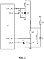
- Fig. 3 shows a simplified, fragmentary schematic diagram of a guard circuit for monitoring the timing behavior or timing behavior of a microcontroller according to a first embodiment.
- circuit arrangement is opposite to in Fig. 1 shown configuration by a doubling of circuit parts improved, and therefore includes a (multi-channel) microcontroller .mu.C known per se, in addition to commonly available inputs and outputs or ports, at least a first analog-to-digital converter input ADC_IN1, a second analog-digital Converter input ADC_IN2, a first digital output or digital output DO_1 and a second digital output or digital output DO_2.
- a microcontroller .mu.C known per se, in addition to commonly available inputs and outputs or ports, at least a first analog-to-digital converter input ADC_IN1, a second analog-digital Converter input ADC_IN2, a first digital output or digital output DO_1 and a second digital output or digital output DO_2.
- a first and a second guard voltage generating section are shown, which are connected at least to the first analog-to-digital converter input ADC_IN1 and the first output DO_1 or the second analog-to-digital converter input ADC_IN2 and the second output DO_2 and at least one first transistor T1 or , a second transistor T2, a first capacitor C1 and a second capacitor C2, a first first resistor R1 and a second first resistor R2, a diode D1 and a resistor R3 include.
- the first and second guard voltage generating sections are constructed identically or identically.
- a first terminal of the transistor T1 for example the drain or collector terminal, is connected to the first input ADC_IN1 of the microcontroller ⁇ C, and a second terminal of the transistor T1, for example the gate or base terminal, is connected to the digital output DO_1.
- the first terminal of the transistor T1 is connected to a second end of the first first resistor R1 and a first terminal of the first capacitor C1.
- a second end of the first first resistor R1 is connected to a reference voltage U Ref , which is provided via the diode D1, for example a suitable zener diode.
- the diode D1 is connected in parallel to the series circuit of the first first resistor R1 and the first capacitor C1 and is from the resistor R3 from a supply voltage Vcc, for example 5V of an electronic control unit (ECU), in which both the microcontroller .mu.C and the guard voltage generating sections arranged or integrated, supplied.
- Vcc for example 5V of an electronic control unit (ECU)
- ECU electronice control unit
- a second terminal of the first capacitor C1 and the anode side of the diode D1 are connected to a common node at a ground potential.
- a first terminal of the second transistor T2 is connected to the second input ADC_IN2 of the microcontroller ⁇ C, and is a second terminal of the second transistor T2, for example the gate or base terminal, to the second digital output DO_2 of the microcontroller ⁇ Cs connected.
- the first terminal of the second transistor T2 is connected to a second end of the second first resistor R2 and a first terminal of the second capacitor C2.
- a second end of the second first resistor R2 is connected to a reference voltage U Ref , which is provided via the diode D1, for example a suitable zener diode.
- the diode D1 is connected in parallel with the series connection of the second first resistor R2 and the second capacitor C2 and is supplied by the resistor R3 from the supply voltage Vcc of, for example, 5V of the electronic control unit (ECU) in which both the microcontroller ⁇ C and the guard voltage generating sections are arranged or integrated supplies.
- a third terminal of the second transistor T2 (source or emitter), a second terminal of the second capacitor C2 and the anode side of the diode D1 may be connected to a common node at a ground potential.
- the above-described transistors T1 and / or T2 which operate in the described configuration as discharge transistors for the capacitor C1 and C2, in a modification of the present embodiment and as a variant of a microcontroller port also already be integrated in the microcontroller .mu.C.
- the capacitors C1 and / or C2 may be directly connected to the corresponding input and output ports of the microcontroller ⁇ C.
- a ground potential or GND can form such a reference potential
- the reference potential can be chosen arbitrarily in accordance with a detection range of the analog-to-digital converter input of the microcontroller .mu.C Fig. 1 and Fig. 3 shown configuration of at least one of the transistors T1, T2 may be arranged inverted, and in this case, instead of the ground potential and the supply voltage Vcc can be used as the reference potential.
- the first transistor T1 which forms in this configuration a discharge transistor for the first capacitor C1 is parallel to the first capacitor C1 and the series circuit is composed of the first first resistor R1 and the first capacitor C1, which are in this Configuration forms an RC element R1 / C1, in parallel with the diode D1.
- the second transistor T2, which forms in this configuration a discharge transistor for the second capacitor C2 is parallel to the second capacitor C2, and the series circuit of the second first resistor R2 and the second capacitor C2, which in this configuration is an RC Formed R2 / C2, parallel to the diode D1.
- the sample value after t2 can be selected, for example, after 70% of the time t_load and with a sufficient time interval to t1.
- the time constants of the timers R1 / C1 and R2 / C2 are designed differently (R1 * C1 ⁇ R2 * C2). This makes it possible to better distinguish asymmetric disturbances such as common-mode noise or common-mode noise.
- the microcontroller .mu.C can show sporadic clock misfires or a defective drive port DO_1 for the discharge transistor T1. This would leave the first capacitor C1 in this case discharged. This would not be detected correctly if a single-channel microcontroller .mu.C would continue to operate in this state.
- the second capacitor C2 continues to charge and thus gets out of the tolerance band, an error of the aforementioned type can be detected by evaluating the second channel as well.
- Fig. 4 shows sections of typical signal waveforms in the form of voltage waveforms U_C1, U_C2, especially in an error case with redundant channels, at different operating states in the guard circuit according to Fig. 3 , Especially are in Fig. 4 the aforementioned error state of a defective (for example permanently on logical 1) output DO_1 of the microcontroller .mu.C and the time-shifted by t_delta sampling of the individual, with the first and the second Wambaterwoodser Wegungsabrough configured channels shown.
- a defective for example permanently on logical 1
Landscapes
- Engineering & Computer Science (AREA)
- Theoretical Computer Science (AREA)
- Physics & Mathematics (AREA)
- General Physics & Mathematics (AREA)
- General Engineering & Computer Science (AREA)
- Quality & Reliability (AREA)
- Mathematical Physics (AREA)
- Evolutionary Computation (AREA)
- Artificial Intelligence (AREA)
- Automation & Control Theory (AREA)
- Debugging And Monitoring (AREA)
- Measurement Of Current Or Voltage (AREA)
- Electronic Switches (AREA)
- Tests Of Electronic Circuits (AREA)
- Microcomputers (AREA)
- Testing Electric Properties And Detecting Electric Faults (AREA)
Claims (13)
- Montage de contrôle du comportement de timing d'une microunité de commande, comportant- une microunité (µC) de commande, montée pour commander au moins une partie (T1, C1, R1, R3, D1 ; T1, T2, C1, C2, R1, R2, R3, D1) de production d'une tension de surveillance pour produire, d'une manière définie dans le temps, au moins une tension (Uc ; U1, U2) de surveillance et pour détecter et lire, à un instant d'échantillonnage déterminé à l'avance, la tension (Uc ; U1, U2) de surveillance produite et- la au moins une partie (T1, C1, R1, R3, D1 ; T1, T2, C1, C2, R1, R2, R3, D1) de production d'une tension de surveillance, qui est montée pour produire la tension (Uc ; U1, U2) de surveillance pouvant être détectée par échantillonnage par la microunité de commande à un instant d'échantillonnage déterminé à l'avance, une tension (Uc, U1, U2) de surveillance détectée à l'instant d'échantillonnage et se trouvant dans une plage de tolérance de tension définie à l'avance, indiquant un état sans défaut de la microunité (µC) de commande, et une tension (Uc ; U1, U2) de surveillance, détectée à l'instant déterminé à l'avance et se trouvant à l'extérieur de la plage de tolérance de tension déterminée à l'avance, indiquant un état défectueux de la microunité (µC) de commande, dans lequela) la partie (T1, C1, R1, R3, D1 ; T1, T2, C1, C2, R1, R2, R3, D1) de production d'une tension de surveillance a au moins un condensateur (C1 ; C1, C2) auquel est appliquée la tension (Uc ; U1, U2) de surveillance et dans lequelb) la partie (T1, C1, R1, R3, D1 ; T1, T2, C1, C2, R1, R2, R3, D1) de production d'une tension de surveillance a au moins un interrupteur (T1 ; T1, T2) électronique, qui est monté en parallèle au condensateur (C1 ; C1, C2) et qui, en fonction d'un état logique à une sortie (DO ; DO_1, DO_2) de la microunité (µC) de commande, peut être commuté de manière commandée dans le temps par la microunité (µC) de commande, dans lequel, pendant un état de 0 logique de la sortie (DO ; DO_1, DO_2), l'interrupteur (T1 ; T1, T2) électronique est bloqué et le condensateur (C1 ; C1, C2) peut être chargé de manière définie et, pendant un état de 1 logique de la sortie (DO ; DO_1, DO_2), l'interrupteur (T1 ; T1, T2) électronique est passant et le condensateur (C1 ; C1, C2) peut être déchargé de manière définie, et dans lequelc) le condensateur (C1 ; C1, C2) est monté de manière à ce que, commandé par la microunité (µC) de commande, par l'intermédiaire de l'interrupteur (T1 ; T1, T2) électronique, il soit déchargé complètement à un instant quelconque et de manière à être, à partir de l'état déchargé, chargé à un instant (t0) déterminé à l'avance, la tension du condensateur et, à un instant d'échantillonnage venant ensuite, la tension (Uc U1, U2) de surveillance appliquée au condensateur (C1 ; C1, C2) provenant d'une équation définissant une courbe de charge
 d) il est prévu une première partie (T1, C1, R1, R3) de production d'une tension de surveillance, dans laquelle- une première résistance (R1) est montée en série avec un premier condensateur (C1) et il s'applique, à une première de ses extrémités, une tension (URef) de référence et elle est reliée, à une seconde de ses extrémités, à une première borne du premier condensateur (C1) ;- il est prévu une résistance (R3) d'alimentation à une première extrémité de laquelle s'applique une tension d'alimentation et qui est reliée, à une seconde de ses extrémités, du côté de la cathode, à une diode (Dl), qui applique la tension (URef) de référence entre la première extrémité de la première première résistance (R1) et une deuxième borne du premier condensateur (C1) et- un premier interrupteur (T1) électronique a une première borne, qui est reliée à la première borne du premier condensateur (C1) et a une première entrée (ADC_IN1) de convertisseur analogique de la microunité (µC) de commande, une deuxième borne, qui est reliée à une première sortie (DO_1) de la microunité (µC) de commande et une troisième borne, qui est reliée, par la deuxième borne du premier condensateur (C1) du côté de la cathode, à la diode (D1) et à un potentiel de référence, etil est prévu une deuxième partie (T2, C2, R2, R3, D1) de production d'une tension de surveillance, dans laquelle- une deuxième première résistance (R2) est montée en série avec un deuxième condensateur (C2) et il s'applique, à une première de ses extrémités, une tension (URef) de référence et elle est reliée, à une seconde de ses extrémités, à une première borne du deuxième condensateur (C2),- la résistance (R3) d'alimentation applique la tension (URef) de référence entre la première extrémité de la deuxième première résistance (R2) et une deuxième borne du deuxième condensateur (C2) et- un deuxième interrupteur (T2) électronique a une première borne, qui est reliée à la première borne du deuxième condensateur (C2) et à une deuxième entrée (ADC_IN2) de convertisseur analogique de la microunité (µC) de commande, une deuxième borne, qui est reliée à une deuxième sortie (DO_2) de la microunité (µC) de commande et une troisième borne, qui est reliée à la deuxième borne du deuxième condensateur (C2) et un potentiel de référence, dans lequel- la première partie (T1, C1, R1, R3) de production d'une tension de surveillance et la deuxième partie (T2, C2, R2, R3, D1) de production d'une tension de surveillance constitue un montage de surveillance à plusieurs canaux.
 - Montage suivant la revendication 1, caractérisé en ce que la première partie (T1, C1, R1, R3) de production d'une tension de surveillance et la deuxième partie de production d'une tension de surveillance sont commandées et échantillonnées d'une manière déphasée, de manière à ce que l'une des tensions (U1) de surveillance soit détectée à l'un des condensateurs (C1) à un premier temps (t1) déterminé à l'avance et soit lue par la microunité (µC) de commande et qu'une autre des tensions (U2) de surveillance soit détectée à un autre des condensateurs (C2), à un deuxième temps (t2 = t1 + Δt) déterminé à l'avance, et soit lue par la microunité (µC) de commande.
- Montage suivant l'une des revendications précédentes, caractérisé en ce que la constante de temps du relais temporisateur défini par la première première résistance (R1) et le premier condensateur (C1) et la constante de temps du relais temporisateur défini par la deuxième première résistance (R2) et le deuxième condensateur (C2) sont différentes l'une de l'autre.
- Montage suivant l'une des revendications précédentes, caractérisé en ce que des échantillonnages de la courbe de charge du condensateur (C1 ; C1, C2) sont répétés cycliquement à des temps d'échantillonnage définis.
- Montage suivant l'une des revendications précédentes, caractérisé en ce que la microunité (µC) de commande est montée de manière à bloquer l'interrupteur (T1 ; T1 ; T2) électronique jusqu'à chargement complet du condensateur (C1 ; C1, C2), à détecter ensuite la valeur absolue de la tension (URef) de référence et, sur la base de la valeur détectée de la tension (URef) de référence, à étalonner au moins un canal de convertisseur analogique-numérique de la microunité (µC) de commande.
- Montage suivant l'une des revendications précédentes, caractérisé en ce que l'interrupteur (T1 ; T1, T2) électronique est constitué sous la forme d'un transistor.
- Montage suivant l'une des revendications précédentes, caractérisé en ce que l'interrupteur électronique est constitué de manière intégrée à la microunité (µC) de commande.
- Montage suivant l'une des revendications 1 à 6, caractérisé en ce que l'interrupteur électronique est prévu à l'extérieur de la microunité (µC) de commande et est relié à celle-ci.
- Procédé de contrôle d'une microunité de commande sur la base d'une tension de surveillance pour contrôler le comportement de timing d'une microunité de commande, qui est produite dans un montage de surveillance suivant l'une des revendications précédentes, caractérisé par les stades :- commande d'au moins une partie (T1, C1, R1, R3, D1 ; T1, T2, C1, C2, R1, R2, R3, D1) de production d'une tension de surveillance pour produire, d'une manière définie dans le temps, au moins une tension (Uc ; U1, U2) de surveillance, la commande comportant une décharge définie d'un condensateur (C1 ; C1, C2) et ensuite la charge, définie en commençant à un instant (t0 ; t1, t2), défini à l'avance, du condensateur (C1 ; C1, C2) suivant une courbe de charge et- la détection et la lecture de la tension de charge produite à un instant d'échantillonnage déterminé à l'avance du condensateur (C1 ; C2, C2) comme tension (Uc ; U1, U2) de surveillance, dans lequel- une tension (Uc ; U1, U2) de surveillance, pouvant être détectée par échantillonnage par la microunité de commande à un instant d'échantillonnage déterminé à l'avance, détectée à l'instant d'échantillonnage et se trouvant dans une plage de tolérance de tension définie à l'avance, indiquant un état sans défaut de la microunité (µC) de commande, et une tension (Uc ; U1, U2) de surveillance, détectée à l'instant déterminé à l'avance et se trouvant à l'extérieur de la plage de tolérance de tension déterminée à l'avance, indiquant un état défectueux de la microunité (µC) de commande, dans lequel- on commande et on échantillonne, de manière déphasée la première partie (T1, C1, R1, R3) de production d'une tension de surveillance et la deuxième partie de production d'une tension de surveillance, en ce que l'une des tensions (U1) de surveillance est détectée sur l'un des condensateurs (C1) à un premier temps (t1) déterminé et est lue par la microunité (µC) de commande et en ce qu'une autre des tensions (U2) de surveillance est détectée sur un autre des condensateurs (C2) à un deuxième temps (t2 = t1 + Δt) déterminé à l'avance et est lue par la micro-unité (µC) de commande ou dans lequel- une constante de temps du relais temporisateur RC de la première partie (T1, C1, R1, R3) de production d'une tension de surveillance et une constante de temps du relais temporisateur RC de la deuxième partie de production d'une tension de surveillance sont différentes l'une de l'autre.
- Procédé suivant la revendication 9, caractérisé en ce que, pendant un état de 0 logique d'une sortie (DO ; DO_1, DO_2) de la microunité de commande, on bloque un interrupteur (T1 ; T1, T2) électronique et le condensateur (C1 ; C1, C2) peut être chargé de manière définie et, pendant un état de 1 logique de la sortie (DO ; DO_1, DO_2) de l'interrupteur (T1 ; T1, T2) électronique, on le rend passant et le condensateur (C1 ; C1, C2) peut être déchargé de manière définie.
- Procédé suivant la revendication 10, caractérisé en ce que le condensateur (C1 ; C1, C2) est, commandé par la microunité (µC) de commande par l'intermédiaire de l'interrupteur (T1 ; T1, T2) électronique, déchargé complètement à un instant quelconque et, à partir de l'état déchargé, est chargé à un instant (t0) défini à l'avance, la tension du condensateur et, à un instant d'échantillonnage venant ensuite, la tension (Uc U1, U2) de surveillance appliquée au condensateur (C1 ; C1, C2) provenant d'une équation définissant une courbe de charge

- Procédé suivant l'une des revendication 9 à 11, caractérisé en ce que l'on répète des échantillonnages de la courbe de charge du condensateur (C1 ; C1, C2) cycliquement à des temps d'échantillonnage définis.
- Procédé suivant l'une des revendications 9 à 12, caractérisé en ce que l'on bloque l'interrupteur (T1 ; T1, T2) électronique jusqu'à charge complète du condensateur (C1 ; C1, C2), on détecte ensuite la valeur absolue de la tension (URef) de référence et, sur la base de la valeur détectée de la tension (URef) de référence, on étalonne au moins un canal de convertisseur analogique-numérique de la microunité (µC) de commande.
Applications Claiming Priority (2)
| Application Number | Priority Date | Filing Date | Title |
|---|---|---|---|
| DE102015117977.6A DE102015117977A1 (de) | 2015-10-22 | 2015-10-22 | Schaltungsanordnung und Verfahren zur Überwachung eines Mikrocontrollers auf der Grundlage einer Wächterspannung |
| PCT/EP2016/074979 WO2017067928A1 (fr) | 2015-10-22 | 2016-10-18 | Agencement de circuits et procédé de surveillance d'un microcontrôleur à base d'une tension de surveillance |
Publications (2)
| Publication Number | Publication Date |
|---|---|
| EP3365784A1 EP3365784A1 (fr) | 2018-08-29 |
| EP3365784B1 true EP3365784B1 (fr) | 2019-08-21 |
Family
ID=57208261
Family Applications (1)
| Application Number | Title | Priority Date | Filing Date |
|---|---|---|---|
| EP16787765.3A Active EP3365784B1 (fr) | 2015-10-22 | 2016-10-18 | Agencement de circuits et procédé de surveillance d'un microcontrôleur à base d'une tension de surveillance |
Country Status (6)
| Country | Link |
|---|---|
| US (1) | US10915387B2 (fr) |
| EP (1) | EP3365784B1 (fr) |
| CN (1) | CN108139956B (fr) |
| DE (1) | DE102015117977A1 (fr) |
| RU (1) | RU2697027C1 (fr) |
| WO (1) | WO2017067928A1 (fr) |
Families Citing this family (2)
| Publication number | Priority date | Publication date | Assignee | Title |
|---|---|---|---|---|
| CN109343992B (zh) * | 2018-09-27 | 2020-09-01 | 浙江大学 | 应用于通用主控芯片的灵活可配的模数转换器控制方法 |
| CN111400074A (zh) * | 2019-01-02 | 2020-07-10 | 珠海格力电器股份有限公司 | 一种模拟看门狗装置及其控制方法 |
Family Cites Families (14)
| Publication number | Priority date | Publication date | Assignee | Title |
|---|---|---|---|---|
| JPS5451454A (en) | 1977-09-30 | 1979-04-23 | Toshiba Corp | Analog digital conversion unit |
| US4586179A (en) * | 1983-12-09 | 1986-04-29 | Zenith Electronics Corporation | Microprocessor reset with power level detection and watchdog timer |
| JPH07291091A (ja) * | 1994-04-28 | 1995-11-07 | Nippondenso Co Ltd | 制御用コンピュータの誤動作防止回路 |
| WO1998007089A1 (fr) | 1996-08-12 | 1998-02-19 | Papst-Motoren Gmbh & Co. Kg | Procedure et installation de surveillance d'un microprocesseur |
| DE19731086C2 (de) | 1997-07-19 | 2001-09-13 | Satronic Ag Dielsdorf | Elektronische Sicherheitsschaltung |
| US7051332B2 (en) * | 2001-05-21 | 2006-05-23 | Cyberscan Technology, Inc. | Controller having a restart engine configured to initiate a controller restart cycle upon receipt of a timeout signal from a watchdog timer |
| RU2261470C1 (ru) * | 2004-03-01 | 2005-09-27 | Федеральное государственное унитарное предприятие "Научно-производственное предприятие "Полет" | Устройство программного управления |
| DE102007045509B4 (de) * | 2007-09-24 | 2011-06-22 | Continental Automotive GmbH, 30165 | Fahrzeug-Steuereinheit mit einem Versorgungspannungsüberwachten Mikrocontroller sowie zugehöriges Verfahren |
| US7884678B2 (en) * | 2009-01-14 | 2011-02-08 | Nuvoton Technology Corporation | Single-pin RC oscillator |
| JP2012003644A (ja) * | 2010-06-21 | 2012-01-05 | Fujitsu Ltd | メモリエラー箇所検出装置、及びメモリエラー箇所検出方法。 |
| US9823280B2 (en) * | 2011-12-21 | 2017-11-21 | Microchip Technology Incorporated | Current sensing with internal ADC capacitor |
| DE102012224348A1 (de) * | 2012-06-25 | 2014-01-02 | Osram Gmbh | Beleuchtungsanlage mit einer Schnittstelle aufweisend ein Netzgerät und mindestens ein Lichtquellenmodul |
| DE102013226429A1 (de) * | 2013-12-18 | 2015-06-18 | Robert Bosch Gmbh | Vorrichtung und Verfahren zur Überwachung eines Zeitgebers |
| CN104330666A (zh) | 2014-10-28 | 2015-02-04 | 陕西千山航空电子有限责任公司 | 一种超级电容组中电容单体故障定位装置和方法 |
-
2015
- 2015-10-22 DE DE102015117977.6A patent/DE102015117977A1/de active Pending
-
2016
- 2016-10-18 RU RU2018118424A patent/RU2697027C1/ru active
- 2016-10-18 WO PCT/EP2016/074979 patent/WO2017067928A1/fr not_active Ceased
- 2016-10-18 US US15/769,613 patent/US10915387B2/en active Active
- 2016-10-18 EP EP16787765.3A patent/EP3365784B1/fr active Active
- 2016-10-18 CN CN201680061973.3A patent/CN108139956B/zh active Active
Non-Patent Citations (1)
| Title |
|---|
| None * |
Also Published As
| Publication number | Publication date |
|---|---|
| US20180314245A1 (en) | 2018-11-01 |
| BR112018007904A2 (pt) | 2018-10-30 |
| EP3365784A1 (fr) | 2018-08-29 |
| US10915387B2 (en) | 2021-02-09 |
| DE102015117977A1 (de) | 2017-04-27 |
| CN108139956A (zh) | 2018-06-08 |
| RU2697027C1 (ru) | 2019-08-08 |
| CN108139956B (zh) | 2021-12-31 |
| WO2017067928A1 (fr) | 2017-04-27 |
Similar Documents
| Publication | Publication Date | Title |
|---|---|---|
| EP3844854B1 (fr) | Bloc-batterie ainsi que procédé de charge pour un bloc-batterie | |
| EP3265754B1 (fr) | Dispositif de pont de mesure avec détection d'erreur améliorée | |
| EP3637114A1 (fr) | Système de haut voltage et procédé de surveillance des erreurs d'isolation dans un système de haut voltage | |
| DE102011086412B4 (de) | Vorrichtung und Verfahren zum Testen des Zustands der Verbindung einer mit einem Verbindungspunkt verbundenen Last | |
| DE2854549C2 (fr) | ||
| EP3186889B1 (fr) | Capteur capacitif, circuit d'interprétation correspondant et actionneur pour un véhicule automobile | |
| EP3649476B1 (fr) | Dispositif et procédé permettant de vérifier une aptitude à fonctionner d'une résistance d'un système de batterie | |
| DE102021111771A1 (de) | Diagnosefähige Schaltungsanordnung, Sensorvorrichtung mit einer Schaltungsanordnung und Verfahren zur Diagnose einer Schaltungsanordnung und/oder Sensorvorrichtung | |
| DE102014219130B4 (de) | Diagnoseschaltung und Verfahren zum Betreiben einer Diagnoseschaltung | |
| WO2017067928A1 (fr) | Agencement de circuits et procédé de surveillance d'un microcontrôleur à base d'une tension de surveillance | |
| EP3233578B1 (fr) | Dispositif de surveillance pour au moins un circuit d'allumage pour un moyen de protection de personnes pour un véhicule, et procédé servant à faire fonctionner un dispositif de surveillance | |
| DE102019129802A1 (de) | Kapazitive Sensorvorrichtung, Verfahren zum Betrieb einer kapazitiven Sensorvorrichtung, Bedienvorrichtung und Fahrzeug | |
| EP1032519B1 (fr) | Cablage pour un composant de reglage, et procede de controle de ce cablage de composant de reglage | |
| DE19631972C2 (de) | Verfahren zum Überwachen der Funktionsfähigkeit eines zur Digitalisierung von Analogsignalen ausgelegten Analog/-Digital Wandlers | |
| DE4409286C1 (de) | Verfahren zum Erkennen der Ursache eines Reset-Vorgangs eines durch einen Mikroprozessor gesteuerten Systems sowie Schaltung zum Durchführen des Verfahrens | |
| EP1423719B1 (fr) | Procede et dispositif pour controler une unite de detection | |
| DE102021111734A1 (de) | Diagnosefähige Schaltungsanordnung und Verfahren zur Diagnose einer Schaltungsanordnung | |
| EP2090945B1 (fr) | Composant de saisie et procédé de détection d'erreurs | |
| EP4028783A1 (fr) | Capteur de batterie | |
| DE10027096A1 (de) | Sensorvorrichtung | |
| DE102010031096A1 (de) | Verfahren und Vorrichtung zum Prüfen eines Schaltkreises | |
| DE102008043254A1 (de) | Integrierter Schaltkreis zur Spannungsüberwachung | |
| WO2022083998A1 (fr) | Analyse d'erreur dans un capteur | |
| EP4593289A1 (fr) | Capteur de proximité inductif, système de capteur comprenant des capteurs de proximité inductif et procédé de fonctionnement d'un tel système de capteur | |
| EP4439099A1 (fr) | Circuit de capteur et système de mesure pour capteurs capacitifs |
Legal Events
| Date | Code | Title | Description |
|---|---|---|---|
| STAA | Information on the status of an ep patent application or granted ep patent |
Free format text: STATUS: UNKNOWN |
|
| STAA | Information on the status of an ep patent application or granted ep patent |
Free format text: STATUS: THE INTERNATIONAL PUBLICATION HAS BEEN MADE |
|
| PUAI | Public reference made under article 153(3) epc to a published international application that has entered the european phase |
Free format text: ORIGINAL CODE: 0009012 |
|
| STAA | Information on the status of an ep patent application or granted ep patent |
Free format text: STATUS: REQUEST FOR EXAMINATION WAS MADE |
|
| 17P | Request for examination filed |
Effective date: 20180522 |
|
| AK | Designated contracting states |
Kind code of ref document: A1 Designated state(s): AL AT BE BG CH CY CZ DE DK EE ES FI FR GB GR HR HU IE IS IT LI LT LU LV MC MK MT NL NO PL PT RO RS SE SI SK SM TR |
|
| AX | Request for extension of the european patent |
Extension state: BA ME |
|
| DAV | Request for validation of the european patent (deleted) | ||
| DAX | Request for extension of the european patent (deleted) | ||
| GRAP | Despatch of communication of intention to grant a patent |
Free format text: ORIGINAL CODE: EPIDOSNIGR1 |
|
| RIC1 | Information provided on ipc code assigned before grant |
Ipc: G06F 11/07 20060101AFI20190131BHEP Ipc: G01R 31/00 20060101ALI20190131BHEP |
|
| STAA | Information on the status of an ep patent application or granted ep patent |
Free format text: STATUS: GRANT OF PATENT IS INTENDED |
|
| INTG | Intention to grant announced |
Effective date: 20190307 |
|
| GRAS | Grant fee paid |
Free format text: ORIGINAL CODE: EPIDOSNIGR3 |
|
| GRAA | (expected) grant |
Free format text: ORIGINAL CODE: 0009210 |
|
| STAA | Information on the status of an ep patent application or granted ep patent |
Free format text: STATUS: THE PATENT HAS BEEN GRANTED |
|
| AK | Designated contracting states |
Kind code of ref document: B1 Designated state(s): AL AT BE BG CH CY CZ DE DK EE ES FI FR GB GR HR HU IE IS IT LI LT LU LV MC MK MT NL NO PL PT RO RS SE SI SK SM TR |
|
| REG | Reference to a national code |
Ref country code: GB Ref legal event code: FG4D Free format text: NOT ENGLISH |
|
| REG | Reference to a national code |
Ref country code: CH Ref legal event code: EP |
|
| REG | Reference to a national code |
Ref country code: DE Ref legal event code: R096 Ref document number: 502016006233 Country of ref document: DE |
|
| REG | Reference to a national code |
Ref country code: AT Ref legal event code: REF Ref document number: 1170535 Country of ref document: AT Kind code of ref document: T Effective date: 20190915 |
|
| REG | Reference to a national code |
Ref country code: IE Ref legal event code: FG4D Free format text: LANGUAGE OF EP DOCUMENT: GERMAN |
|
| REG | Reference to a national code |
Ref country code: SE Ref legal event code: TRGR |
|
| REG | Reference to a national code |
Ref country code: LT Ref legal event code: MG4D |
|
| REG | Reference to a national code |
Ref country code: NL Ref legal event code: MP Effective date: 20190821 |
|
| PG25 | Lapsed in a contracting state [announced via postgrant information from national office to epo] |
Ref country code: LT Free format text: LAPSE BECAUSE OF FAILURE TO SUBMIT A TRANSLATION OF THE DESCRIPTION OR TO PAY THE FEE WITHIN THE PRESCRIBED TIME-LIMIT Effective date: 20190821 Ref country code: BG Free format text: LAPSE BECAUSE OF FAILURE TO SUBMIT A TRANSLATION OF THE DESCRIPTION OR TO PAY THE FEE WITHIN THE PRESCRIBED TIME-LIMIT Effective date: 20191121 Ref country code: NL Free format text: LAPSE BECAUSE OF FAILURE TO SUBMIT A TRANSLATION OF THE DESCRIPTION OR TO PAY THE FEE WITHIN THE PRESCRIBED TIME-LIMIT Effective date: 20190821 Ref country code: HR Free format text: LAPSE BECAUSE OF FAILURE TO SUBMIT A TRANSLATION OF THE DESCRIPTION OR TO PAY THE FEE WITHIN THE PRESCRIBED TIME-LIMIT Effective date: 20190821 Ref country code: NO Free format text: LAPSE BECAUSE OF FAILURE TO SUBMIT A TRANSLATION OF THE DESCRIPTION OR TO PAY THE FEE WITHIN THE PRESCRIBED TIME-LIMIT Effective date: 20191121 Ref country code: PT Free format text: LAPSE BECAUSE OF FAILURE TO SUBMIT A TRANSLATION OF THE DESCRIPTION OR TO PAY THE FEE WITHIN THE PRESCRIBED TIME-LIMIT Effective date: 20191223 Ref country code: FI Free format text: LAPSE BECAUSE OF FAILURE TO SUBMIT A TRANSLATION OF THE DESCRIPTION OR TO PAY THE FEE WITHIN THE PRESCRIBED TIME-LIMIT Effective date: 20190821 |
|
| PG25 | Lapsed in a contracting state [announced via postgrant information from national office to epo] |
Ref country code: IS Free format text: LAPSE BECAUSE OF FAILURE TO SUBMIT A TRANSLATION OF THE DESCRIPTION OR TO PAY THE FEE WITHIN THE PRESCRIBED TIME-LIMIT Effective date: 20191221 Ref country code: LV Free format text: LAPSE BECAUSE OF FAILURE TO SUBMIT A TRANSLATION OF THE DESCRIPTION OR TO PAY THE FEE WITHIN THE PRESCRIBED TIME-LIMIT Effective date: 20190821 Ref country code: ES Free format text: LAPSE BECAUSE OF FAILURE TO SUBMIT A TRANSLATION OF THE DESCRIPTION OR TO PAY THE FEE WITHIN THE PRESCRIBED TIME-LIMIT Effective date: 20190821 Ref country code: RS Free format text: LAPSE BECAUSE OF FAILURE TO SUBMIT A TRANSLATION OF THE DESCRIPTION OR TO PAY THE FEE WITHIN THE PRESCRIBED TIME-LIMIT Effective date: 20190821 Ref country code: GR Free format text: LAPSE BECAUSE OF FAILURE TO SUBMIT A TRANSLATION OF THE DESCRIPTION OR TO PAY THE FEE WITHIN THE PRESCRIBED TIME-LIMIT Effective date: 20191122 Ref country code: AL Free format text: LAPSE BECAUSE OF FAILURE TO SUBMIT A TRANSLATION OF THE DESCRIPTION OR TO PAY THE FEE WITHIN THE PRESCRIBED TIME-LIMIT Effective date: 20190821 |
|
| PG25 | Lapsed in a contracting state [announced via postgrant information from national office to epo] |
Ref country code: TR Free format text: LAPSE BECAUSE OF FAILURE TO SUBMIT A TRANSLATION OF THE DESCRIPTION OR TO PAY THE FEE WITHIN THE PRESCRIBED TIME-LIMIT Effective date: 20190821 |
|
| PG25 | Lapsed in a contracting state [announced via postgrant information from national office to epo] |
Ref country code: RO Free format text: LAPSE BECAUSE OF FAILURE TO SUBMIT A TRANSLATION OF THE DESCRIPTION OR TO PAY THE FEE WITHIN THE PRESCRIBED TIME-LIMIT Effective date: 20190821 Ref country code: EE Free format text: LAPSE BECAUSE OF FAILURE TO SUBMIT A TRANSLATION OF THE DESCRIPTION OR TO PAY THE FEE WITHIN THE PRESCRIBED TIME-LIMIT Effective date: 20190821 Ref country code: DK Free format text: LAPSE BECAUSE OF FAILURE TO SUBMIT A TRANSLATION OF THE DESCRIPTION OR TO PAY THE FEE WITHIN THE PRESCRIBED TIME-LIMIT Effective date: 20190821 Ref country code: PL Free format text: LAPSE BECAUSE OF FAILURE TO SUBMIT A TRANSLATION OF THE DESCRIPTION OR TO PAY THE FEE WITHIN THE PRESCRIBED TIME-LIMIT Effective date: 20190821 |
|
| PG25 | Lapsed in a contracting state [announced via postgrant information from national office to epo] |
Ref country code: CZ Free format text: LAPSE BECAUSE OF FAILURE TO SUBMIT A TRANSLATION OF THE DESCRIPTION OR TO PAY THE FEE WITHIN THE PRESCRIBED TIME-LIMIT Effective date: 20190821 Ref country code: IS Free format text: LAPSE BECAUSE OF FAILURE TO SUBMIT A TRANSLATION OF THE DESCRIPTION OR TO PAY THE FEE WITHIN THE PRESCRIBED TIME-LIMIT Effective date: 20200224 Ref country code: MC Free format text: LAPSE BECAUSE OF FAILURE TO SUBMIT A TRANSLATION OF THE DESCRIPTION OR TO PAY THE FEE WITHIN THE PRESCRIBED TIME-LIMIT Effective date: 20190821 Ref country code: SK Free format text: LAPSE BECAUSE OF FAILURE TO SUBMIT A TRANSLATION OF THE DESCRIPTION OR TO PAY THE FEE WITHIN THE PRESCRIBED TIME-LIMIT Effective date: 20190821 Ref country code: SM Free format text: LAPSE BECAUSE OF FAILURE TO SUBMIT A TRANSLATION OF THE DESCRIPTION OR TO PAY THE FEE WITHIN THE PRESCRIBED TIME-LIMIT Effective date: 20190821 |
|
| REG | Reference to a national code |
Ref country code: CH Ref legal event code: PL |
|
| REG | Reference to a national code |
Ref country code: DE Ref legal event code: R097 Ref document number: 502016006233 Country of ref document: DE |
|
| PLBE | No opposition filed within time limit |
Free format text: ORIGINAL CODE: 0009261 |
|
| STAA | Information on the status of an ep patent application or granted ep patent |
Free format text: STATUS: NO OPPOSITION FILED WITHIN TIME LIMIT |
|
| PG2D | Information on lapse in contracting state deleted |
Ref country code: IS |
|
| PG25 | Lapsed in a contracting state [announced via postgrant information from national office to epo] |
Ref country code: LU Free format text: LAPSE BECAUSE OF NON-PAYMENT OF DUE FEES Effective date: 20191018 Ref country code: CH Free format text: LAPSE BECAUSE OF NON-PAYMENT OF DUE FEES Effective date: 20191031 Ref country code: LI Free format text: LAPSE BECAUSE OF NON-PAYMENT OF DUE FEES Effective date: 20191031 |
|
| 26N | No opposition filed |
Effective date: 20200603 |
|
| REG | Reference to a national code |
Ref country code: BE Ref legal event code: MM Effective date: 20191031 |
|
| PG25 | Lapsed in a contracting state [announced via postgrant information from national office to epo] |
Ref country code: SI Free format text: LAPSE BECAUSE OF FAILURE TO SUBMIT A TRANSLATION OF THE DESCRIPTION OR TO PAY THE FEE WITHIN THE PRESCRIBED TIME-LIMIT Effective date: 20190821 Ref country code: BE Free format text: LAPSE BECAUSE OF NON-PAYMENT OF DUE FEES Effective date: 20191031 |
|
| PG25 | Lapsed in a contracting state [announced via postgrant information from national office to epo] |
Ref country code: FR Free format text: LAPSE BECAUSE OF NON-PAYMENT OF DUE FEES Effective date: 20191021 Ref country code: IE Free format text: LAPSE BECAUSE OF NON-PAYMENT OF DUE FEES Effective date: 20191018 |
|
| PG25 | Lapsed in a contracting state [announced via postgrant information from national office to epo] |
Ref country code: CY Free format text: LAPSE BECAUSE OF FAILURE TO SUBMIT A TRANSLATION OF THE DESCRIPTION OR TO PAY THE FEE WITHIN THE PRESCRIBED TIME-LIMIT Effective date: 20190821 |
|
| GBPC | Gb: european patent ceased through non-payment of renewal fee |
Effective date: 20201018 |
|
| PG25 | Lapsed in a contracting state [announced via postgrant information from national office to epo] |
Ref country code: MT Free format text: LAPSE BECAUSE OF FAILURE TO SUBMIT A TRANSLATION OF THE DESCRIPTION OR TO PAY THE FEE WITHIN THE PRESCRIBED TIME-LIMIT Effective date: 20190821 Ref country code: HU Free format text: LAPSE BECAUSE OF FAILURE TO SUBMIT A TRANSLATION OF THE DESCRIPTION OR TO PAY THE FEE WITHIN THE PRESCRIBED TIME-LIMIT; INVALID AB INITIO Effective date: 20161018 |
|
| PG25 | Lapsed in a contracting state [announced via postgrant information from national office to epo] |
Ref country code: GB Free format text: LAPSE BECAUSE OF NON-PAYMENT OF DUE FEES Effective date: 20201018 |
|
| PG25 | Lapsed in a contracting state [announced via postgrant information from national office to epo] |
Ref country code: MK Free format text: LAPSE BECAUSE OF FAILURE TO SUBMIT A TRANSLATION OF THE DESCRIPTION OR TO PAY THE FEE WITHIN THE PRESCRIBED TIME-LIMIT Effective date: 20190821 |
|
| REG | Reference to a national code |
Ref country code: AT Ref legal event code: MM01 Ref document number: 1170535 Country of ref document: AT Kind code of ref document: T Effective date: 20211018 |
|
| PG25 | Lapsed in a contracting state [announced via postgrant information from national office to epo] |
Ref country code: AT Free format text: LAPSE BECAUSE OF NON-PAYMENT OF DUE FEES Effective date: 20211018 |
|
| P01 | Opt-out of the competence of the unified patent court (upc) registered |
Effective date: 20230528 |
|
| PGFP | Annual fee paid to national office [announced via postgrant information from national office to epo] |
Ref country code: DE Payment date: 20251028 Year of fee payment: 10 |
|
| PGFP | Annual fee paid to national office [announced via postgrant information from national office to epo] |
Ref country code: IT Payment date: 20251024 Year of fee payment: 10 |
|
| PGFP | Annual fee paid to national office [announced via postgrant information from national office to epo] |
Ref country code: SE Payment date: 20251024 Year of fee payment: 10 |