EP3367411A1 - Circuit de diagnostic de relais - Google Patents
Circuit de diagnostic de relais Download PDFInfo
- Publication number
- EP3367411A1 EP3367411A1 EP18158237.0A EP18158237A EP3367411A1 EP 3367411 A1 EP3367411 A1 EP 3367411A1 EP 18158237 A EP18158237 A EP 18158237A EP 3367411 A1 EP3367411 A1 EP 3367411A1
- Authority
- EP
- European Patent Office
- Prior art keywords
- relay
- voltage
- output
- voltage divider
- comparator
- Prior art date
- Legal status (The legal status is an assumption and is not a legal conclusion. Google has not performed a legal analysis and makes no representation as to the accuracy of the status listed.)
- Granted
Links
Images




Classifications
-
- H—ELECTRICITY
- H01—ELECTRIC ELEMENTS
- H01H—ELECTRIC SWITCHES; RELAYS; SELECTORS; EMERGENCY PROTECTIVE DEVICES
- H01H47/00—Circuit arrangements not adapted to a particular application of the relay and designed to obtain desired operating characteristics or to provide energising current
- H01H47/002—Monitoring or fail-safe circuits
-
- G—PHYSICS
- G01—MEASURING; TESTING
- G01R—MEASURING ELECTRIC VARIABLES; MEASURING MAGNETIC VARIABLES
- G01R31/00—Arrangements for testing electric properties; Arrangements for locating electric faults; Arrangements for electrical testing characterised by what is being tested not provided for elsewhere
- G01R31/327—Testing of circuit interrupters, switches or circuit-breakers
- G01R31/3271—Testing of circuit interrupters, switches or circuit-breakers of high voltage or medium voltage devices
- G01R31/3272—Apparatus, systems or circuits therefor
-
- B—PERFORMING OPERATIONS; TRANSPORTING
- B60—VEHICLES IN GENERAL
- B60L—PROPULSION OF ELECTRICALLY-PROPELLED VEHICLES; SUPPLYING ELECTRIC POWER FOR AUXILIARY EQUIPMENT OF ELECTRICALLY-PROPELLED VEHICLES; ELECTRODYNAMIC BRAKE SYSTEMS FOR VEHICLES IN GENERAL; MAGNETIC SUSPENSION OR LEVITATION FOR VEHICLES; MONITORING OPERATING VARIABLES OF ELECTRICALLY-PROPELLED VEHICLES; ELECTRIC SAFETY DEVICES FOR ELECTRICALLY-PROPELLED VEHICLES
- B60L3/00—Electric devices on electrically-propelled vehicles for safety purposes; Monitoring operating variables, e.g. speed, deceleration or energy consumption
- B60L3/0023—Detecting, eliminating, remedying or compensating for drive train abnormalities, e.g. failures within the drive train
- B60L3/0046—Detecting, eliminating, remedying or compensating for drive train abnormalities, e.g. failures within the drive train relating to electric energy storage systems, e.g. batteries or capacitors
-
- B—PERFORMING OPERATIONS; TRANSPORTING
- B60—VEHICLES IN GENERAL
- B60L—PROPULSION OF ELECTRICALLY-PROPELLED VEHICLES; SUPPLYING ELECTRIC POWER FOR AUXILIARY EQUIPMENT OF ELECTRICALLY-PROPELLED VEHICLES; ELECTRODYNAMIC BRAKE SYSTEMS FOR VEHICLES IN GENERAL; MAGNETIC SUSPENSION OR LEVITATION FOR VEHICLES; MONITORING OPERATING VARIABLES OF ELECTRICALLY-PROPELLED VEHICLES; ELECTRIC SAFETY DEVICES FOR ELECTRICALLY-PROPELLED VEHICLES
- B60L58/00—Methods or circuit arrangements for monitoring or controlling batteries or fuel cells, specially adapted for electric vehicles
- B60L58/10—Methods or circuit arrangements for monitoring or controlling batteries or fuel cells, specially adapted for electric vehicles for monitoring or controlling batteries
-
- G—PHYSICS
- G01—MEASURING; TESTING
- G01R—MEASURING ELECTRIC VARIABLES; MEASURING MAGNETIC VARIABLES
- G01R31/00—Arrangements for testing electric properties; Arrangements for locating electric faults; Arrangements for electrical testing characterised by what is being tested not provided for elsewhere
- G01R31/005—Testing of electric installations on transport means
- G01R31/006—Testing of electric installations on transport means on road vehicles, e.g. automobiles or trucks
-
- G—PHYSICS
- G01—MEASURING; TESTING
- G01R—MEASURING ELECTRIC VARIABLES; MEASURING MAGNETIC VARIABLES
- G01R31/00—Arrangements for testing electric properties; Arrangements for locating electric faults; Arrangements for electrical testing characterised by what is being tested not provided for elsewhere
- G01R31/327—Testing of circuit interrupters, switches or circuit-breakers
- G01R31/3271—Testing of circuit interrupters, switches or circuit-breakers of high voltage or medium voltage devices
- G01R31/3275—Fault detection or status indication
-
- G—PHYSICS
- G01—MEASURING; TESTING
- G01R—MEASURING ELECTRIC VARIABLES; MEASURING MAGNETIC VARIABLES
- G01R31/00—Arrangements for testing electric properties; Arrangements for locating electric faults; Arrangements for electrical testing characterised by what is being tested not provided for elsewhere
- G01R31/327—Testing of circuit interrupters, switches or circuit-breakers
- G01R31/3277—Testing of circuit interrupters, switches or circuit-breakers of low voltage devices, e.g. domestic or industrial devices, such as motor protections, relays, rotation switches
- G01R31/3278—Testing of circuit interrupters, switches or circuit-breakers of low voltage devices, e.g. domestic or industrial devices, such as motor protections, relays, rotation switches of relays, solenoids or reed switches
-
- H—ELECTRICITY
- H01—ELECTRIC ELEMENTS
- H01H—ELECTRIC SWITCHES; RELAYS; SELECTORS; EMERGENCY PROTECTIVE DEVICES
- H01H47/00—Circuit arrangements not adapted to a particular application of the relay and designed to obtain desired operating characteristics or to provide energising current
- H01H47/001—Functional circuits, e.g. logic, sequencing, interlocking circuits
-
- Y—GENERAL TAGGING OF NEW TECHNOLOGICAL DEVELOPMENTS; GENERAL TAGGING OF CROSS-SECTIONAL TECHNOLOGIES SPANNING OVER SEVERAL SECTIONS OF THE IPC; TECHNICAL SUBJECTS COVERED BY FORMER USPC CROSS-REFERENCE ART COLLECTIONS [XRACs] AND DIGESTS
- Y02—TECHNOLOGIES OR APPLICATIONS FOR MITIGATION OR ADAPTATION AGAINST CLIMATE CHANGE
- Y02T—CLIMATE CHANGE MITIGATION TECHNOLOGIES RELATED TO TRANSPORTATION
- Y02T10/00—Road transport of goods or passengers
- Y02T10/60—Other road transportation technologies with climate change mitigation effect
- Y02T10/70—Energy storage systems for electromobility, e.g. batteries
Definitions
- the present invention generally relates to relays and, more particularly, to a relay diagnostic circuit.
- the diagnosis of a relay state is an important function of new energy electric vehicles, which can diagnose and find risks in the event of adhesion, open circuit and other abnormal state of the relay timely, and can carry out alarm, protection and other actions before safety accidents, so as to significantly reduce the loss of personal property due to relay failure.
- the diagnosis of a relay state is an important function of new energy electric vehicles, which can diagnose and find risks in the event of adhesion, open circuit and other abnormal state of the relay timely, and can carry out alarm, protection and other actions before safety accidents, so as to significantly reduce the loss of personal property due to relay failure.
- the conventional relay diagnostic circuit at least has the following disadvantages.
- a method of voltage sampling of the relay contacts is used instead of using a relay with auxiliary contacts in the conventional relay diagnostic circuits.
- the failure of the relay can be determined via the sampling voltage.
- the voltage sampling circuit of this method is complex and expensive, and the failure judgment logic is complicated.
- the cross voltages are sampled on the inside of the main positive relay and the inside of the main negative relay in conventional relay diagnostic circuits.
- a voltage difference between the relay contacts is formed by a sampling resistor to assist testing status.
- outside circuit of the relay will form a potential reverse current path due to cross voltage sampling, and if the circuit forms a negative voltage which is applied to a high voltage device which is sensitive to the negative voltage eventually, it will cause damage to the high voltage equipment.
- One object of the present invention is to provide a relay diagnostic circuit which can avoid potential reverse current problems in cross voltage sampling.
- a relay diagnostic circuit for a number of relays connected in series between an electric vehicle power supply end and a load or a charging end includes a number of voltage divider branches connected to a same reference ground, an isolation unit and a judgment unit, wherein each of the voltage divider branches is configured to obtain a voltage of one end of each relay and output the voltage after dividing the voltage; the isolation unit is configured to isolate and convert a number of divider voltages output from the number of voltage divider branches and output the voltages output to the judgment unit; and the judgment unit is configured to compare a comparison information of the divider voltages at two ends of each relay with a corresponding driving state of the relay and obtain a diagnosis result of each relay.
- each of the voltage divider branches includes at least two divider resistors in series, a connection point of the divider resistor is an output end of the voltage divider branch to output the divider voltage, each relay corresponds to two voltage divider branches, a first end of each relay is connected to one end of a corresponding voltage divider branch, a second end of the relay is connected to one end of another corresponding voltage divider branch, and other ends of all voltage divider branches are connected to a same reference ground.
- the isolation unit includes optocouplers, driving ends of the optocouplers are connected to corresponding output ends of the voltage divider branches respectively, and output ends of the optocouplers are connected to input end of the judgment unit.
- the isolation unit includes an isolation chip, input ends of the isolation chip are connected to corresponding output ends of the voltage divider branches respectively, and the output ends of the isolation chip are connected to an input end of the judgment unit.
- the relay diagnostic circuit further includes a comparison unit configured to compare divider voltages output from two voltage divider branches at both ends of a same relay, output the comparison information to the isolation unit, and output the comparison information to the judgment unit after isolation and conversion of the isolation unit.
- the comparison unit includes a number of comparator groups, each comparator group includes a forward comparator and a reverse comparator, two comparators of a same comparator group corresponds to a same relay, output ends of one of the voltage divider branches for obtaining output voltage of the first end of corresponding relay is connected to a positive input end of the forward comparator and a negative input end of the reverse comparator, output ends of the other voltage divider branch for obtaining output voltage of the second end corresponding to the relay is connected to the negative input end of the forward comparator and the positive input end of the reverse comparator, output ends of the forward comparator and the reverse comparator of each comparator group are connected as a output end of the comparator group, and output ends of each comparator group are connected to input end of the isolation unit respectively.
- the relay diagnostic circuit further includes an analog-to-digital conversion unit configured to convert the divider voltage output from a voltage divider branch into digital information and output the digital information to the isolation unit, and output the digital information to the judgment unit after isolation and conversion of the isolation unit.
- the analog-to-digital conversion unit is an analog-to-digital conversion chip, input ends of the analog-to-digital conversion chip are connected to corresponding output ends of the voltage divider branches respectively, and output ends of the analog-to-digital conversion chip are connected to input end of the isolation unit.
- the analog-to-digital conversion unit is a slave MCU
- input ends of the slave MCU are connected to corresponding output ends of the voltage divider branches respectively
- the output ends of the slave MCU are connected to the input end of the isolation unit.
- the judgment unit is a master MCU and an input end of the master MCU is connect to an output end of the isolation unit.
- the relay diagnostic circuit according to the present invention has the following advantages.
- the two reference grounds in the cross voltage sampling are combined into a reference ground by optimizing the resistance topology, so as to avoid the problem of potential reverse current.
- the reliability of the circuit has been improved by replacing the ADC sampling chip with a comparator chip to reduce circuit complexity.
- the reliability of the circuit has been improved by combining the two isolated power supplies in the cross voltage sampling into one isolated power supply to reduce circuit complexity.
- comparator logic output judgments rather than the numerical operations and logical judgments after ADC sampling can significantly reduce the computational complexity.
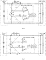
- a relay diagnostic circuit for a number of relays 11 connected in series between an electric vehicle power supply end 12 and a load or a charging end 13 includes: a number of voltage divider branches connected to a same reference ground 14, an isolation unit 15 and a judgment unit 16, wherein:
- each voltage divider branches 14 obtains the voltages at two ends of the relay 11 and outputs the voltage by voltage dividing, and the judgment unit 16 is prevented from being affected by the isolation unit 15.
- the present invention realizes the detection of the state of the relay.
- the two reference grounds in cross voltage sampling are combined into a reference ground by optimizing the resistance topology so as to avoid the problem of potential reverse current.
- the circuit reliability has been improved.
- each of the voltage divider branches includes at least two voltage divider resistors in series, the connection point of the voltage divider resistors is the output end of the voltage divider branch to output the divider voltage, each relay corresponds to two voltage divider branches, the first end of each relay is connected to one end of a corresponding voltage divider branch, the second end of the relay is connected to one end of another corresponding voltage divider branch, and the other ends of all voltage divider branches are connected to a same reference ground.
- the power supply end is a battery pack for electric vehicles
- the load or the charging end is a high voltage load (such as DC/DC, motor drive, etc.).
- the battery pack is directly connected to the high voltage load through a main positive relay S 11 and the main negative relay S 13 for energy transmission.
- the voltage divider resistors R12, R13 and R14, R15 form two voltage divider branches to obtain two voltages at both ends of the main positive relay S11 and the precharge relay S12 respectively, and divide the voltage.
- the voltage divider resistors R16, R17 and R18, R19 form two voltage divider branches to obtain two voltages at both ends of the main negative relay S13 respectively, and divide the voltage.
- the voltage divider branches of the voltage divider resistors R12, R13 and R14, R15 and the voltage divider branches of the voltage divider resistors R16, R17 and R18, R19 have a same reference ground.
- the voltage difference across the contacts of the main positive relay S11 is reflected in V11 and V12 by the voltage divider resistors R12, R13 and R14, R15 connected to the reference GND.
- the voltage difference across the contacts of the main negative relay S 13 is reflected in V13 and V14 by the voltage divider resistors R16, R17 and R18, R19 connected to the reference GND.
- the power supply end is a battery pack for electric vehicles
- the load or the charging end is a charger (such as DC charging pile)
- the battery pack is directly connected to the charger through the charging positive relay S21 and the charging negative relay S23 for energy transmission.
- the voltage divider resistors R22, R23 and R24, R25 form two voltage divider branches to obtain two voltages at both ends of the main positive relay S21 and the precharge relay S22 respectively, and divide the voltage
- the voltage divider resistors R26, R27 and R28, R29 form two voltage divider branches to obtain two voltages at both ends of the main negative relay S23 respectively, and divide the voltage.
- the voltage divider branches of the voltage divider resistors R22, R23 and R24, R25 and the voltage divider branches of the voltage divider resistors R26, R27 and R28, R29 have a same reference ground.
- the voltage difference across the contacts of the main positive relay S21 is reflected in V21 and V22 by the voltage divider resistors R22, R23 and R24, R25 connected to the reference GND.
- the voltage difference across the contacts of the main negative relay S23 is reflected in V23 and V24 by the voltage divider resistors R26, R27 and R28, R29 connected to the reference GND.
- the power supply end is a high voltage power supply
- the load or the charging end is a high voltage load (such as motor drives)
- the high voltage power supply is directly connected to the high voltage load through the main positive relay S31 and the main negative relay S33 for energy transmission.
- the voltage divider resistors R32, R33 and R34, R35 form two voltage divider branches to obtain two voltages at both ends of the main positive relay S31 and the precharge relay S32 respectively, and divide the voltage.
- the voltage divider resistors R36, R37 and R38, R39 from two voltage divider branches to obtain two voltages at both ends of the main negative relay S33 respectively, and divide the voltage.
- the voltage divider branches of the voltage divider resistors R32, R33 and R34, R35 and the voltage divider branches of the voltage divider resistors R36, R37 and R38, R39 have the same reference ground.
- the voltage difference across the contacts of the main positive relay S31 is reflected in V31 and V32 by the voltage divider resistors R32, R33 and R34, R35 connected to the reference GND.
- the voltage difference across the contacts of the main negative relay S33 is reflected in V33 and V34 by the voltage divider resistors R36, R37 and R38, R39 connected to the reference GND.
- the power supply end is a battery pack for electric vehicles
- the load or the charging end is a high voltage load (such as DC/DC, motor drive, etc.)
- the battery pack is directly connected to the high voltage load through the main positive relay S41 and the main negative relay S43 for energy transmission.
- the precharge relay S42 and the precharge resistor R41 it is necessary to precharge the input capacitance of the high voltage load before closing the main positive relay S41, and the precharge is achieved by the precharge relay S42 and the precharge resistor R41.
- the voltage divider resistors R42, R43 and R44, R45 form two voltage divider branches to obtain two voltages at both ends of the main positive relay S41 and the precharge relay S42 respectively, and divide the voltage.
- the voltage divider resistors R46, R47 and R48, R49 form two voltage divider branches to obtain two voltages at both ends of the main negative relay S43 respectively, and divide the voltage.
- the voltage divider branches of the voltage divider resistors R42, R43 and R44, R45 and the voltage divider branches of the voltage divider resistors R46, R47 and R48, R49 have the same reference ground.
- the voltage difference across the contacts of the main positive relay S41 is reflected in V41 and V42 by the voltage divider resistors R42, R43 and R44, R45 connected to the reference GND.
- the voltage difference across the contacts of the main negative relay S43 is reflected in V43 and V44 by the voltage divider resistors R46, R47 and R48, R49 connected to the reference GND.
- the power supply end is a battery pack for electric vehicles
- the load or the charging end is a high voltage load (such as DC/DC, motor drive, etc.)
- the battery pack is directly connected to the high voltage load through the main positive relay S51 and the main negative relay S53 for energy transmission.
- the precharge relay S52 and the precharge resistor R51 it is necessary to precharge the input capacitance of the high voltage load before closing the main positive relay S51, and the precharge is achieved by the precharge relay S52 and the precharge resistor R51.
- the voltage divider resistors R52, R53 and R54, R55 form two voltage divider branches to obtain two voltages at both ends of the main positive relay S51 and the precharge relay S52 respectively, and divide the voltage.
- the voltage divider resistors R56, R57 and R58, R59 form two voltage divider branches to obtain two voltages at both ends of the main negative relay S53 respectively, and divide the voltage.
- the voltage divider branches of the voltage divider resistors R52, R53 and R54, R55 and the voltage divider branches of the voltage divider resistors R56, R57 and R58, R59 have the same reference ground.
- the voltage difference across the contacts of the main positive relay S51 is reflected in V51 and V52 by the voltage divider resistors R52, R53 and R54, R55 connected to the reference GND.
- the voltage difference across the contacts of the main negative relay S53 is reflected in V53 and V54 by the voltage divider resistors R56, R57 and R58, R59 connected to the reference GND.
- the power supply end is a battery pack for electric vehicles
- the load or the charging end is a high voltage load (such as DC/DC, motor drive, etc.)
- the battery pack is directly connected to the high voltage load through the main positive relay S61 and the main negative relay S63 for energy transmission.
- the precharge relay S62 and the precharge resistor R61 it is necessary to precharge the input capacitance of the high voltage load before closing the main positive relay S61, and the precharge is achieved by the precharge relay S62 and the precharge resistor R61.
- the voltage divider resistors R62, R63 and R64, R65 form two voltage divider branches to obtain two voltages at both ends of the main positive relay S61 and the precharge relay S62 respectively, and divide the voltage.
- the voltage divider resistors R66, R67 and R68, R69 form two voltage divider branches to obtain two voltages at both ends of the main negative relay S63 respectively, and divide the voltage.
- the voltage divider branches of the voltage divider resistors R62, R63 and R64, R65 and the voltage divider branches of the voltage divider resistors R66, R67 and R68, R69 have the same reference ground.
- the voltage difference across the contacts of the main positive relay S61 is reflected in V61 and V62 by the voltage divider resistors R62, R63 and R64, R65 connected to the reference GND.
- the voltage difference across the contacts of the main negative relay S63 is reflected in V63 and V64 by the voltage divider resistors R66, R67 and R68, R69 connected to the reference GND.
- the power supply end is a battery pack for electric vehicles
- the load or the charging end is a high voltage load (such as DC/DC, motor drive, etc.)
- the battery pack is directly connected to the high voltage load through the main positive relay S71 and the main negative relay S73 for energy transmission.
- the precharge relay S72 and the precharge resistor R71 it is necessary to precharge the input capacitance of the high voltage load before closing the main positive relay S71, and the precharge is achieved by the precharge relay S72 and the precharge resistor R71.
- the voltage divider resistors R72, R73 and R74, R75 form two voltage divider branches to obtain two voltages at both ends of the main positive relay S71 and the precharge relay S72 respectively, and divide the voltage.
- the voltage divider resistors R76, R77 and R78, R79 form two voltage divider branches to obtain two voltages at both ends of the main negative relay S73 respectively, and divide the voltage.
- the voltage divider branches of the voltage divider resistors R72, R73 and R74, R75 and the voltage divider branches of the voltage divider resistors R76, R77 and R78, R79 have the same reference ground.
- the voltage difference across the contacts of the main positive relay S71 is reflected in V71 and V72 by the voltage divider resistors R72, R73 and R74, R75 connected to the reference GND.
- the voltage difference across the contacts of the main negative relay S73 is reflected in V73 and V74 by the voltage divider resistors R76, R77 and R78, R79 connected to the reference GND.
- the power supply end is a battery pack for electric vehicles
- the load or the charging end is a high voltage load (such as DC/DC, motor drive, etc.), DC charger, accessories and so on.
- the battery pack is directly connected to the high voltage load through the main positive relay K82 and the main negative relay K81 for energy transmission.
- the precharge relay K83 and the precharge resistor In general, it is necessary to precharge the input capacitance of the high voltage load before closing the main positive relay K82, and the precharge is achieved by the precharge relay K83 and the precharge resistor.
- the battery pack is connected through the accessories relay K86 and the main negative relay K81 for energy transmission with the accessories.
- the battery pack is directly connected to the DC charger through the charging positive relay K85 and the charging negative relay K84 for energy transmission.
- the battery pack is connected to a heating film therein through the heating positive relay K88 and the heating negative relay K87 for energy transmission.
- the divider voltages of the main positive replay K82 are reflected in V82 and V85
- the divider voltages of the main negative replay K81 are reflected in V88 and V86
- the divider voltages of the charging negative relay K84 are reflected in V88 and V87
- the divider voltages of the charging positive relay K85 are reflected in V82 and V83
- the divider voltages of the the accessories relay K86 are reflected in V82 and V84
- the divider voltages of the heating negative relay K87 are reflected in V88 and V89
- the divider voltages of the heating positive relay K88 are reflected in V82 and V81.
- the isolation unit includes optocouplers, the driving ends of the optocouplers are respectively connected to the output ends of the voltage divider branches, and the output ends of the optocouplers are connected to the input ends of the judgment unit.
- isolation is realized via the optocouplers U13, U23 and U33.
- the isolation unit includes an isolation chip, and the input ends of the isolation chip are connected to the output ends of the voltage divider branches respectively, and the output ends of the isolation chip are connected to the input end of the judgment unit.
- the voltage difference across the contacts of the main positive relay S41 is relatively large, which makes the voltage difference reflected in V41 and V42 by the voltage divider resistors R42, R43 and R44, R45 connected to the reference GND relatively large.
- the output voltage signals V41 and V42 are input to the comparison circuit composed of comparator U41, comparator U42 and the like, resulting in a combined output signal: pull-down.
- the pull-down signal from the comparison circuit is converted to a low level and input to the digital isolation chip U43 so that the corresponding output pin of the U43 also outputs a low level signal.
- the low level signal from U43 will be detected by MCU, and the main positive relay S41 and the precharge relay S42 will be diagnosed as in a state of non-adhesion in view of the driving state of the relay.
- the voltage difference across the contacts of the main positive relay S41 is closes to zero, which makes the voltage difference reflected in V41 and V42 by the voltage divider resistors R42, R43 and R44, R45 connected to the reference GND closes to zero.
- the output voltage signals V41 and V42 are input to a comparison circuit composed of comparator U41, comparator U42 and the like, resulting in a combined output signal: high impedance.
- the high impedance signal from the comparison circuit will be converted to the high level and input to the digital isolation chip U43 so that the corresponding output pin of the U43 also outputs a high level signal.
- the high level signal from U43 will be detected by MCU, and the main positive relay S41 or the precharge relay S42 will be diagnosed as in the state of adhesion in view of the driving state of the relay.
- the voltage difference across the contacts of the main negative relay S43 is relatively large, which makes the voltage difference reflected in V43 and V44 by the voltage divider resistors R46, R47 and R48, R49 connected to the reference GND relatively large.
- the output voltage signals V43 and V44 are input to the comparison circuit composed of comparator U44, comparator U45 and the like, resulting in a combined output signal: pull-down.
- the pull-down signal from the comparison circuit is converted to the low level input to the digital isolation chip U46 so that the corresponding output pin of the U46 also outputs a low level signal.
- the low level signal from U46 will be detected by the MCU, and the main negative relay S43 will be diagnosed in the state of non-adhesion in view of the driving state of the relay.
- the voltage difference across the contacts of the main negative relay S43 is closes to zero, which makes the voltage difference reflected in V43 and V44 by the voltage divider resistors R46, R47 and R48, R49 connected to the reference GND closes to zero.
- the output voltage signals V43 and V44 are input to the comparison circuit composed of comparator U44, comparator U45 and the like, resulting in a combined output signal: high impedance.
- the high impedance signal from the comparison circuit will be converted to the high level input to the digital isolation chip U46 so that the corresponding output pin of the U46 also outputs the high level signal.
- the high level signal from U46 will be detected by the MCU, and the main negative relay S43 will be diagnosed in the state of adhesion in view of the driving state of the relay.
- the voltage difference across the contacts of the main positive relay S41 is closes to zero, which makes the voltage difference reflected in V41 and V42 by the voltage divider resistors R42, R43 and R44, R45 connected to the reference GND closes to zero.
- the output voltage signals V41 and V42 are input to the comparison circuit composed of comparator U41, comparator U42 and the like, resulting in a combined output signal: high impedance.
- the high impedance signal from the comparison circuit will be converted to the high level input to the digital isolation chip U43 so that the corresponding output pin of the U43 also outputs the high level signal.
- the high level signal from U43 will be detected by the MCU, and the main positive relay S41 has not been in the state of open circuit failure which will be diagnosed in view of the driving state of the relay.
- the voltage difference across the contacts of the main positive relay S41 is relatively large, which makes the voltage difference reflected in V41 and V42 by the voltage divider resistors R42, R43 and R44, R45 connected to the reference GND relatively large.
- the output voltage signals V41 and V42 are input to the comparison circuit composed of comparator U41, comparator U42 and the like, resulting in a combined output signal: pull-down.
- the pull-down signal from the comparison circuit will be converted to a low level input to the digital isolation chip U43 so that the corresponding output pin of the U43 also outputs the low level signal.
- the low level signal from U43 will be detected by the MCU, and the main positive relay S41 has been in the state of open circuit failure which will be diagnosed in view of the driving state of the relay.
- the voltage difference across the contacts of the main negative relay S43 is closes to zero, which makes the voltage difference reflected in V43 and V44 by the voltage divider resistors R46, R47 and R48, R49 connected to the reference GND closes to zero.
- the output voltage signals V43 and V44 are input to the comparison circuit composed of comparator U44, comparator U45 and the like, resulting in a combined output signal: high impedance.
- the high impedance signal from the comparison circuit will be converted to a high level input to the digital isolation chip U46 so that the corresponding output pin of the U46 also outputs the high level signal.
- the high level signal from U46 will be detected by the MCU, and the main negative relay S43 has not been in the state of open circuit failure which will be diagnosed in view of the driving state of the relay.
- the voltage difference across the contacts of the main negative relay S43 is relatively large, which makes the voltage difference reflected in V43 and V44 by the voltage divider resistors R46, R47 and R48, R49 connected to the reference GND relatively large.
- the output voltage signals V43 and V44 are input to the comparison circuit composed of comparator U44, comparator U45 and the like, resulting in a combined output signal: pull-down.
- the pull-down signal from the comparison circuit will be converted to a low level input to the digital isolation chip U46 so that the corresponding output pin of the U46 also outputs the low level signal.
- the low level signal from U46 will be detected by the MCU, and the main negative relay S43 has been in the state of open circuit failure which will be diagnosed in view of the driving state of the relay.
- the voltage difference across the contacts of the main positive relay S51 is relatively large, which makes the voltage difference reflected in V51 and V52 by the voltage divider resistors R52, R53 and R54, R55 connected to the reference GND relatively large.
- the output voltage signals V51 and V52 are input to the comparison circuit composed of comparator U51, comparator U52 and the like, resulting in a combined output signal: pull-down.
- the pull-down signal from the comparison circuit is converted to a low level input to the slave MCU U56 which will detect the state of the signal and transmit the information of the state to the master MCU U57 through the digital isolation chip U53.
- the main positive relay S51 and the precharge relay S52 will be diagnosed in the state of non-adhesion in view of the driving state of the relay by the master MCU U57.
- the voltage difference across the contacts of the main positive relay S51 is closes to zero, which makes the voltage difference reflected in V51 and V52 by the voltage divider resistors R52, R53 and R54, R55 connected to the reference GND closes to zero.
- the output voltage signals V51 and V52 are input to the comparison circuit composed of comparator U51, comparator U52 and the like, resulting in a combined output signal: high impedance.
- the high impedance signal from the comparison circuit is converted to a high level input to the slave MCU U56 which will detect the state of the signal and transmit the information of the state to the master MCU U57 through the digital isolation chip U53.
- the main positive relay S51 or the precharge relay S52 will be diagnosed in the state of adhesion in view of the driving state of the relay by the master MCU U57.
- the main negative relay S53 When the main negative relay S53 is in the state of disconnection and has not been in the state of adhesion failure, the voltage difference across the contacts of the main negative relay S53 is relatively large, which makes the voltage difference reflected in V53 and V54 by the voltage divider resistors R56, R57 and R58, R59 connected to the reference GND relatively large.
- the output voltage signals V53 and V54 are input to the comparison circuit composed of comparator U54, comparator U55 and the like, resulting in a combined output signal: pull-down.
- the pull-down signal from the comparison circuit is converted to a low level input to the slave MCU U56 which will detect the state of the signal and transmit the information of the state to the master MCU U57 through the digital isolation chip U53.
- the main negative relay S53 will be diagnosed in the state of non-adhesion in view of the driving state of the relay by the master MCU U57.
- the main negative relay S53 When the main negative relay S53 is in the state of disconnection and has been in the state of adhesion failure, the voltage difference across the contacts of the main negative relay S53 is closes to zero, which makes the voltage difference reflected in V53 and V54 by the voltage divider resistors R56, R57 and R58, R59 connected to the reference GND closes to zero.
- the output voltage signals V53 and V54 are input to the comparison circuit composed of comparator U54, comparator U55 and the like, resulting in a combined output signal: high impedance.
- the high impedance signal from the comparison circuit is converted to a high level input to the slave MCU U56 which will detect the state of the signal and transmit the information of the state to the master MCU U57 through the digital isolation chip U53.
- the main negative relay S53 will be diagnosed in the state of adhesion in view of the driving state of the relay by the master MCU U57.
- the main positive relay S51 When the main positive relay S51 is closed and has not been in the state of open circuit failure, the voltage difference across the contacts of the main positive relay S51 is closes to zero, which makes the voltage difference reflected in V51 and V52 by the voltage divider resistors R52, R53 and R54, R55 connected to the reference GND closes to zero.
- the output voltage signals V51 and V52 are input to the comparison circuit composed of comparator U51, comparator U52 and the like, resulting in a combined output signal: high impedance.
- the high impedance signal from the comparison circuit is converted to a high level input to the slave MCU U56 which will detect the state of the signal and transmit the information of the state to the master MCU U57 through the digital isolation chip U53.
- the main positive relay S51 has not been in the state of open circuit failure which will be diagnosed in view of the driving state of the relay by the master MCU U57.
- the main positive relay S51 When the main positive relay S51 is closed and has been in the state of open circuit failure, the voltage difference across the contacts of the main positive relay S51 is relatively large, which makes the voltage difference reflected in V51 and V52 by the voltage divider resistors R52, R53 and R54, R55 connected to the reference GND relatively large.
- the output voltage signals V51 and V52 are input to the comparison circuit composed of comparator U51, comparator U52 and the like, resulting in a combined output signal: pull-down.
- the pull-down signal from the comparison circuit is converted to a low level input to the slave MCU U56 which will detect the state of the signal and transmit the information of the state to the master MCU U57 through the digital isolation chip U53.
- the main positive relay S51 has been in the state of open circuit failure which will be diagnosed in view of the driving state of the relay by the master MCU U57.
- the main negative relay S53 When the main negative relay S53 is closed and has not been in the state of open circuit failure, the voltage difference across the contacts of the main negative relay S53 is closes to zero, which makes the voltage difference reflected in V53 and V54 by the voltage divider resistors R56, R57 and R58, R59 connected to the reference GND closes to zero.
- the output voltage signals V53 and V54 are input to the comparison circuit composed of comparator U54, comparator U55 and the like, resulting in a combined output signal: high impedance.
- the high impedance signal from the comparison circuit is converted to a high level input to the slave MCU U56 which will detect the state of the signal and transmit the information of the state to the master MCU U57 through the digital isolation chip U53.
- the main negative relay S53 has not been in the state of open circuit failure which will be diagnosed in view of the driving state of the relay by the master MCU U57.
- the main negative relay S53 When the main negative relay S53 is closed and has been in the state of open circuit failure, the voltage difference across the contacts of the main negative relay S53 is relatively large, which makes the voltage difference reflected in V53 and V54 by the voltage divider resistors R56, R57 and R58, R59 connected to the reference GND relatively large.
- the output voltage signals V53 and V54 are input to the comparison circuit composed of comparator U54, comparator U55 and the like, resulting in a combined output signal: pull-down.
- the pull-down signal from the comparison circuit is converted to a low level input to the slave MCU U56 which will detect the state of the signal and transmit the information of the state to the master MCU U57 through the digital isolation chip U53.
- the main negative relay S53 has been in the state of open circuit failure which will be diagnosed in view of the driving state of the relay by the master MCU U57.
- the isolation is achieved by access of an isolation chip U63.
- the relay diagnostic circuit further includes a comparison unit configured to compare the divider voltages output from the two voltage divider branches at both ends of the same relay, output the comparison information to the isolation unit, and output the comparison information to the judgment unit after the isolation of the isolation unit.
- the comparison unit includes a number of comparator groups.
- Each comparator group includes a forward comparator and a reverse comparator.
- the two comparators of the same comparator group correspond to the same relay.
- the output end of one of the voltage divider branches for obtaining the output voltage of the first end of the corresponding relay is connected to the positive input end of the forward comparator and the negative input end of the reverse comparator.
- the output end of the other voltage divider branch for obtaining the output voltage of the second end corresponding to the relay is connected to the negative input end of the forward comparator and the positive input end of the reverse comparator.
- the output of the forward comparator and the reverse comparator of each comparator group is connected as the output end of the comparator group.
- the output ends of the comparator groups are respectively connected to the input ends of the isolation unit.
- the voltage difference across the contacts of the main positive relay S11 is relatively large, which makes the voltage difference reflected in V11 and V12 by the voltage divider resistors R12, R13 and R14, R15 connected to the reference GND relatively large.
- the output voltage signals V11 and V12 are input to the comparison circuit composed of comparator U1, comparator U12 and the like, resulting in a combined output signal: pull-down.
- the pull-down signal from the comparison circuit will drive the optocoupler U13 so that the optocoupler U13 also outputs a pull-down signal.
- the MCU will detect a logic low level due to the pull-down signal from the optocoupler U13, and the main positive relay S11 and the precharge relay S12 will be diagnosed in the state of non-adhesion in view of the driving state of the relay by the MCU.
- the voltage difference across the contacts of the main positive relay S11 is closes to zero, which makes the voltage difference reflected in V11 and V12 by the voltage divider resistors R12, R13 and R14, R15 connected to the reference GND closes to zero.
- the output voltage signals V11 and V12 are input to the comparison circuit composed of comparator U11, comparator U12 and the like, resulting in a combined output signal: high impedance.
- the high impedance signal from the comparison circuit will not drive the optocoupler U13 so that the optocoupler U13 also outputs a high impedance signal.
- the MCU will detect a logic high level due to the high impedance signal from the optocoupler U13, and the main positive relay S11 or the precharge relay S12 will be diagnosed in the state of adhesion in view of the driving state of the relay by the MCU.
- the voltage difference across the contacts of the main negative relay S 13 is relatively large, which makes the voltage difference reflected in V13 and V 14 by the voltage divider resistors R16, R17 and R18, R19 connected to the reference GND relatively large.
- the output voltage signals V13 and V14 are input to the comparison circuit composed of comparator U14, comparator U15 and the like, resulting in a combined output signal: pull-down.
- the pull-down signal from the comparison circuit will drive the optocoupler U16 so that the optocoupler U16 also outputs a pull-down signal.
- the MCU will detect a logic low level due to the pull-down signal from the optocoupler U16, and the main negative relay S13 will be diagnosed in the state of non-adhesion in view of the driving state of the relay by the MCU.
- the voltage difference across the contacts of the main negative relay S 13 is closes to zero, which makes the voltage difference reflected in V13 and V14 by the voltage divider resistors R16, R17 and R18, R19 connected to the reference GND closes to zero.
- the output voltage signals V 13 and V 14 are input to the comparison circuit composed of comparator U14, comparator U15 and the like, resulting in a combined output signal: high impedance.
- the high impedance signal from the comparison circuit will not drive the optocoupler U16 so that the optocoupler U16 also outputs a high impedance signal.
- the MCU will detect a logic high level due to the high impedance signal from the optocoupler U16, and the main negative relay S13 will be diagnosed in the state of adhesion in view of the driving state of the relay by the MCU.
- the voltage difference across the contacts of the main positive relay S11 is closes to zero, which makes the voltage difference reflected in V11 and V12 by the voltage divider resistors R12, R13 and R14, R15 connected to the reference GND closes to zero.
- the output voltage signals V11 and V12 are input to the comparison circuit composed of comparator U11, comparator U12 and the like, resulting in a combined output signal: high impedance.
- the high impedance signal from the comparison circuit will not drive the optocoupler U13 so that the optocoupler U13 also outputs a high impedance signal.
- the MCU will detect a logic high level due to the high impedance signal from the optocoupler U13, and the main positive relay S11 has not been in the state of open circuit failure which will be diagnosed in view of the driving state of the relay by the MCU.
- the voltage difference across the contacts of the main positive relay S11 is relatively large, which makes the voltage difference reflected in V11 and V12 by the voltage divider resistors R12, R13 and R14, R15 connected to the reference GND relatively large.
- the output voltage signals V11 and V12 are input to the comparison circuit composed of comparator U11, comparator U12 and the like, resulting in a combined output signal: pull-down.
- the pull-down signal from the comparison circuit will drive the optocoupler U13 so that the optocoupler U13 also outputs a pull-down signal.
- the MCU will detect a logic low level due to the pull-down signal from the optocoupler U13, and the main positive relay S11 has been in the state of open circuit failure which will be diagnosed in view of the driving state of the relay by the MCU.
- the voltage difference across the contacts of the main negative relay S13 is closes to zero, which makes the voltage difference reflected in V13 and V14 by the voltage divider resistors R16, R17 and R18, R19 connected to the reference GND closes to zero.
- the output voltage signals V13 and V14 are input to the comparison circuit composed of comparator U14, comparator U15 and the like, resulting in a combined output signal: high impedance.
- the high impedance signal from the comparison circuit will not drive the optocoupler U16 so that the optocoupler U16 also outputs a high impedance signal.
- the MCU will detect a logic high level due to the high impedance signal from the optocoupler U16, and the main positive relay S 13 has not been in the state of open circuit failure which will be diagnosed in view of the driving state of the relay by the MCU.
- the voltage difference across the contacts of the main negative relay S 13 is relatively large, which makes the voltage difference reflected in V13 and V14 by the voltage divider resistors R16, R17 and R18, R19 connected to the reference GND relatively large.
- the output voltage signals V13 and V14 are input to the comparison circuit composed of comparator U14, comparator U15 and the like, resulting in a combined output signal: pull-down.
- the pull-down signal from the comparison circuit will drive the optocoupler U16 so that the optocoupler U16 also outputs a pull-down signal.
- the MCU will detect a logic low level due to the pull-down signal from the optocoupler U16, and the main negative relay S 13 has been in the state of open circuit failure which will be diagnosed in view of the driving state of the relay by the MCU.
- comparators U21, U22, U24, U25, U31, U32, U34, U35 are comparators U21, U22, U24, U25, U31, U32, U34, U35.
- the relay diagnostic circuit further includes an analog-to-digital conversion unit configured to convert the divider voltage output from the voltage divider branch into digital information and output the digital information to the isolation unit, and output the digital information of the divider voltage to the judgment unit after the isolation and conversion of the isolation unit.
- the analog-to-digital conversion unit is an analog-to-digital conversion chip, and the input ends of the analog-to-digital conversion chip are connected to the output ends of the voltage divider branches respectively, and the output end of the analog-to-digital conversion chip is connected to the input end of the isolation unit.
- the voltage difference across the contacts of the main positive relay S61 is relatively large, which makes the voltage difference reflected in V61 and V62 by the voltage divider resistors R62, R63 and R64, R65 connected to the reference GND relatively large.
- the output voltage signals V61 and V62 are input to the ADC chip U61 and obtain a converted digital quantity.
- the ADC chip U61 sends the digital quantity to the MCU U67 through the digital isolation chip U63 by means of communication.
- the main positive relay S61 and the precharge relay S62 will be diagnosed in the state of non-adhesion in view of the driving state of the relay by the MCU U67.
- the main positive relay S61 and the precharge relay S62 are in the state of disconnection and one of them has been in the state of adhesion failure, the voltage difference across the contacts of the main positive relay S61 is closes to zero, which makes the voltage difference reflected in V61 and V62 by the voltage divider resistors R62, R63 and R64, R65 connected to the reference GND closes to zero.
- the output voltage signals V61 and V62 are input to the ADC chip U61 and obtain a converted digital quantity.
- the ADC chip U61 sends the digital quantity to the MCU U67 through the digital isolation chip U63 by means of communication.
- the main positive relay S61 or the precharge relay S62 will be diagnosed in the state of adhesion in view of the driving state of the relay by the MCU U67.
- the main negative relay S63 When the main negative relay S63 is in the state of disconnection and has not been in the state of adhesion failure, the voltage difference across the contacts of the main negative relay S63 is relatively large, which makes the voltage difference reflected in V63 and V64 by the voltage divider resistors R66, R67 and R68, R69 connected to the reference GND relatively large.
- the output voltage signals V63 and V64 are input to the ADC chip U61 and obtain a converted digital quantity.
- the ADC chip U61 sends the digital quantity to the MCU U67 through the digital isolation chip U63 by means of communication.
- the main negative relay S63 will be diagnosed in the state of non-adhesion in view of the driving state of the relay by the MCU U67.
- the main negative relay S63 When the main negative relay S63 is in the state of disconnection and has been in the state of adhesion failure, the voltage difference across the contacts of the main negative relay S63 is closes to zero, which makes the voltage difference reflected in V63 and V64 by the voltage divider resistors R66, R67 and R68, R69 connected to the reference GND closes to zero.
- the output voltage signals V63 and V64 are input to the ADC chip U61 and obtain a converted digital quantity.
- the ADC chip U61 sends the digital quantity to the MCU U67 through the digital isolation chip U63 by means of communication.
- the main negative relay S63 will be diagnosed in the state of adhesion in view of the driving state of the relay by the MCU U67.
- the main positive relay S61 When the main positive relay S61 is closed and has not been in the state of open circuit failure, the voltage difference across the contacts of the main positive relay S61 is closes to zero, which makes the voltage difference reflected in V61 and V62 by the voltage divider resistors R62, R63 and R64, R65 connected to the reference GND closes to zero.
- the output voltage signals V61 and V62 are input to the ADC chip U61 and obtain a converted digital quantity.
- the ADC chip U61 sends the digital quantity to the MCU U67 through the digital isolation chip U63 by means of communication.
- the main positive relay S61 has not been in the state of open circuit failure which will be diagnosed in view of the driving state of the relay by the MCU U67.
- the main positive relay S61 When the main positive relay S61 is closed and has been in the state of open circuit failure, the voltage difference across the contacts of the main positive relay S61 is relatively large, which makes the voltage difference reflected in V61 and V62 by the voltage divider resistors R62, R63 and R64, R65 connected to the reference GND relatively large.
- the output voltage signals V61 and V62 are input to the ADC chip U61 and obtain a converted digital quantity.
- the ADC chip U61 sends the digital quantity to the MCU U67 through the digital isolation chip U63 by means of communication.
- the main positive relay S61 has been in the state of open circuit failure which will be diagnosed in view of the driving state of the relay by the MCU U67.
- the main negative relay S63 When the main negative relay S63 is closed and has not been in the state of open circuit failure, the voltage difference across the contacts of the main negative relay S63 is closes to zero, which makes the voltage difference reflected in V63 and V64 by the voltage divider resistors R66, R67 and R68, R69 connected to the reference GND closes to zero.
- the output voltage signals V63 and V64 are input to the ADC chip U61 and obtain a converted digital quantity.
- the ADC chip U61 sends the digital quantity to the MCU U67 through the digital isolation chip U63 by means of communication.
- the main negative relay S63 has not been in the state of open circuit failure which will be diagnosed in view of the driving state of the relay by the MCU U67.
- the main negative relay S63 When the main negative relay S63 is closed and has been in the state of open circuit failure, the voltage difference across the contacts of the main negative relay S63 is relatively large, which makes the voltage difference reflected in V63 and V64 by the voltage divider resistors R66, R67 and R68, R69 connected to the reference GND relatively large.
- the output voltage signals V63 and V64 are input to the ADC chip U61 and obtain a converted digital quantity.
- the ADC chip U61 sends the digital quantity to the MCU U67 through the digital isolation chip U63 by means of communication.
- the main negative relay S63 has been in the state of open circuit failure which will be diagnosed in view of the driving state of the relay by the MCU U67.
- the analog-to-digital conversion unit is a slave MCU
- the input ends of the slave MCU are respectively connected to the output ends of the voltage divider branches
- the output end of the slave MCU is connected to the input end of the isolation unit.
- the voltage difference across the contacts of the main positive relay S71 is relatively large, which makes the voltage difference reflected in V71 and V72 by the voltage divider resistors R72, R73 and R74, R75 connected to the reference GND relatively large.
- the output voltage signals V71 and V72 are input to the ADC port of the slave MCU U71 and obtain the converted digital quantity.
- the slave MCU U71 sends the digital quantity to the master MCU U77 through the digital isolation chip U73 by means of communication.
- the main positive relay S71 and the precharge relay S72 will be diagnosed in the state of non-adhesion in view of the driving state of the relay by the master MCU U77.
- the voltage difference across the contacts of the main positive relay S71 is closes to zero, which makes the voltage difference reflected in V71 and V72 by the voltage divider resistors R72, R73 and R74, R75 connected to the reference GND closes to zero.
- the output voltage signals V71 and V72 are input to the ADC port of the slave MCU U71 and obtain the converted digital quantity.
- the slave MCU U71 sends the digital quantity to the master MCU U77 through the digital isolation chip U73 by means of communication.
- the main positive relay S71 or the precharge relay S72 will be diagnosed in the state of adhesion in view of the driving state of the relay by the master MCU U77.
- the main negative relay S73 When the main negative relay S73 is in the state of disconnection and has not been in the state of adhesion failure, the voltage difference across the contacts of the main negative relay S73 is relatively large, which makes the voltage difference reflected in V73 and V74 by the voltage divider resistors R76, R77 and R78, R79 connected to the reference GND relatively large.
- the output voltage signals V73 and V74 are input to the ADC port of the slave MCU U71 and obtain the converted digital quantity.
- the slave MCU U71 sends the digital quantity to the master MCU U77 through the digital isolation chip U73 by means of communication.
- the main negative relay S73 will be diagnosed in the state of non-adhesion in view of the driving state of the relay by the master MCU U77.
- the main negative relay S73 When the main negative relay S73 is in the state of disconnection and has been in the state of adhesion failure, the voltage difference across the contacts of the main negative relay S73 is closes to zero, which makes the voltage difference reflected in V73 and V74 by the voltage divider resistors R76, R77 and R78, R79 connected to the reference GND closes to zero.
- the output voltage signals V73 and V74 are input to the ADC port of the slave MCU U71 and obtain the converted digital quantity.
- the slave MCU U71 sends the digital quantity to the master MCU U77 through the digital isolation chip U73 by means of communication.
- the main negative relay S73 will be diagnosed in the state of adhesion in view of the driving state of the relay by the master MCU U77.
- the main positive relay S71 When the main positive relay S71 is closed and has not been in the state of open circuit failure, the voltage difference across the contacts of the main positive relay S71 is closes to zero, which makes the voltage difference reflected in V71 and V72 by the voltage divider resistors R72, R73 and R74, R75 connected to the reference GND closes to zero.
- the output voltage signals V71 and V72 are input to the ADC port of the slave MCU U71 and obtain the converted digital quantity.
- the slave MCU U71 sends the digital quantity to the master MCU U77 through the digital isolation chip U73 by means of communication.
- the main positive relay S71 has not been in the state of open circuit failure which will be diagnosed in view of the driving state of the relay by the master MCU U77.
- the main positive relay S71 When the main positive relay S71 is closed and has been in the state of open circuit failure, the voltage difference across the contacts of the main positive relay S71 is relatively large, which makes the voltage difference reflected in V71 and V72 by the voltage divider resistors R72, R73 and R74, R75 connected to the reference GND relatively large.
- the output voltage signals V71 and V72 are input to the ADC port of the slave MCU U71 and obtain the converted digital quantity.
- the slave MCU U71 sends the digital quantity to the master MCU U77 through the digital isolation chip U73 by means of communication.
- the main positive relay S71 has been in the state of open circuit failure which will be diagnosed in view of the driving state of the relay by the master MCU U77.
- the main negative relay S73 When the main negative relay S73 is closed and has not been in the state of open circuit failure, the voltage difference across the contacts of the main negative relay S73 is closes to zero, which makes the voltage difference reflected in V73 and V74 by the voltage divider resistors R76, R77 and R78, R79 connected to the reference GND closes to zero.
- the output voltage signals V73 and V74 are input to the ADC port of the slave MCU U71 and obtain the converted digital quantity.
- the slave MCU U71 sends the digital quantity to the master MCU U77 through the digital isolation chip U73 by means of communication.
- the main negative relay S73 has not been in the state of open circuit failure which will be diagnosed in view of the driving state of the relay by the master MCU U77.
- the main negative relay S73 When the main negative relay S73 is closed and has been in the state of open circuit failure, the voltage difference across the contacts of the main negative relay S73 is relatively large, which makes the voltage difference reflected in V73 and V74 by the voltage divider resistors R76, R77 and R78, R79 connected to the reference GND relatively large.
- the output voltage signals V73 and V74 are input to the ADC port of the slave MCU U71 and obtain the converted digital quantity.
- the slave MCU U71 sends the digital quantity to the master MCU U77 through the digital isolation chip U73 by means of communication.
- the main negative relay S73 has been in the state of open circuit failure which will be diagnosed in view of the driving state of the relay by the master MCU U77.
- the judgment unit is a master MCU of U17, U27, U37, U47, U57, U67, U77, and the input end of the master MCU is connected to the output end of the isolation unit.
- the relay diagnostic circuit according to the present invention has the following advantages:
Landscapes
- Engineering & Computer Science (AREA)
- Power Engineering (AREA)
- General Physics & Mathematics (AREA)
- Physics & Mathematics (AREA)
- Life Sciences & Earth Sciences (AREA)
- Sustainable Development (AREA)
- Sustainable Energy (AREA)
- Transportation (AREA)
- Mechanical Engineering (AREA)
- Chemical & Material Sciences (AREA)
- Combustion & Propulsion (AREA)
- Electric Propulsion And Braking For Vehicles (AREA)
- Testing Of Short-Circuits, Discontinuities, Leakage, Or Incorrect Line Connections (AREA)
Applications Claiming Priority (1)
| Application Number | Priority Date | Filing Date | Title |
|---|---|---|---|
| CN201710099308.XA CN108469584A (zh) | 2017-02-23 | 2017-02-23 | 继电器诊断电路 |
Publications (2)
| Publication Number | Publication Date |
|---|---|
| EP3367411A1 true EP3367411A1 (fr) | 2018-08-29 |
| EP3367411B1 EP3367411B1 (fr) | 2019-07-31 |
Family
ID=61256869
Family Applications (1)
| Application Number | Title | Priority Date | Filing Date |
|---|---|---|---|
| EP18158237.0A Active EP3367411B1 (fr) | 2017-02-23 | 2018-02-22 | Circuit de diagnostic de relais |
Country Status (3)
| Country | Link |
|---|---|
| US (1) | US10854405B2 (fr) |
| EP (1) | EP3367411B1 (fr) |
| CN (2) | CN108469584A (fr) |
Cited By (2)
| Publication number | Priority date | Publication date | Assignee | Title |
|---|---|---|---|---|
| EP3451002A1 (fr) * | 2017-08-29 | 2019-03-06 | Contemporary Amperex Technology Co., Limited | Circuit de diagnostic de relais, procédé de diagnostic et système de gestion de batterie |
| WO2023194251A1 (fr) * | 2022-04-07 | 2023-10-12 | Phoenix Contact Gmbh & Co.Kg | Détection d'un état commuté d'un élément de commutation |
Families Citing this family (38)
| Publication number | Priority date | Publication date | Assignee | Title |
|---|---|---|---|---|
| CN107526041A (zh) * | 2017-08-29 | 2017-12-29 | 宁德时代新能源科技股份有限公司 | 电池检测电路和电池管理系统 |
| JP6497475B1 (ja) * | 2018-08-31 | 2019-04-10 | ミツミ電機株式会社 | 二次電池保護回路、二次電池保護装置、電池パック及び二次電池保護回路の制御方法 |
| US11016148B1 (en) * | 2018-09-04 | 2021-05-25 | Kevin Mark Curtis | Self-configuring relay tester |
| CN109143066B (zh) * | 2018-09-04 | 2021-01-08 | 阳光电源(上海)有限公司 | 电机控制器及其采样信号处理方法 |
| CN109188266A (zh) * | 2018-10-11 | 2019-01-11 | 东莞塔菲尔新能源科技有限公司 | 一种高压负极继电器黏连的检测电路及其检测方法 |
| EP3654358B1 (fr) * | 2018-11-15 | 2025-12-31 | Infineon Technologies Austria AG | Circuit de relais de puissance mems |
| CN111319465B (zh) * | 2018-11-29 | 2021-08-17 | 宁德时代新能源科技股份有限公司 | 一种电动车运行中的异常保护装置 |
| CN109739211B (zh) * | 2018-12-29 | 2020-11-03 | 蜂巢能源科技有限公司 | 用于负载电路的诊断系统及电动车 |
| CN109782159B (zh) | 2019-02-25 | 2020-10-16 | 宁德时代新能源科技股份有限公司 | 高压检测电路及其检测方法 |
| CN110470981A (zh) * | 2019-07-26 | 2019-11-19 | 东软睿驰汽车技术(沈阳)有限公司 | 一种确定接触器状态的电路、方法及装置 |
| CN112578273A (zh) * | 2019-09-30 | 2021-03-30 | 江苏万帮德和新能源科技股份有限公司 | 交流电路中继电器的粘连检测装置、方法和交流充电桩 |
| DE102019217056A1 (de) * | 2019-11-06 | 2021-05-06 | Robert Bosch Gmbh | Batteriesystem für ein Elektrofahrzeug, Verfahren zur Diagnose eines Batteriesystems und Elektrofahrzeug |
| CN112858893A (zh) * | 2019-11-28 | 2021-05-28 | 欣旺达电动汽车电池有限公司 | 一种接触器状态检测电路、检测方法以及电池管理系统 |
| US11491932B2 (en) * | 2020-01-22 | 2022-11-08 | Ford Global Technologies, Llc | Integrated components of an electrified vehicle electrical system and electrical distribution method |
| CN113466676B (zh) * | 2020-03-31 | 2022-12-09 | 比亚迪股份有限公司 | 检测开关触点粘连的电路及其检测方法和车辆 |
| JP2021185450A (ja) * | 2020-05-25 | 2021-12-09 | セイコーエプソン株式会社 | リレー故障検出回路およびロボット |
| CN113302505B (zh) * | 2020-07-31 | 2023-02-24 | 华为数字能源技术有限公司 | 车载充电机、方法和电动车辆 |
| CN112098820B (zh) * | 2020-07-31 | 2022-11-18 | 华为数字能源技术有限公司 | 开关状态检测电路、方法和装置 |
| EP3955406A1 (fr) * | 2020-08-10 | 2022-02-16 | Valeo Siemens eAutomotive Norway AS | Système électrique comportant un circuit permettant de protéger un composant électrique contre les courants dommageables |
| WO2022082524A1 (fr) * | 2020-10-21 | 2022-04-28 | 深圳欣锐科技股份有限公司 | Circuit de détection de relais basé sur un échantillonnage différentiel et dispositif de détection |
| DE102020214562A1 (de) * | 2020-11-19 | 2022-05-19 | Robert Bosch Gesellschaft mit beschränkter Haftung | Batteriesystem, Verfahren zur Diagnose eines Batteriesystems und Kraftfahrzeug |
| CN112798947A (zh) * | 2020-12-29 | 2021-05-14 | 东风汽车有限公司 | 电动汽车快充继电器检测电路、检测方法及检测电子设备 |
| CN112798946B (zh) * | 2020-12-29 | 2024-08-02 | 东风汽车有限公司 | 电动汽车快充继电器检测电路的检测方法及检测电子设备 |
| FR3118490B1 (fr) * | 2020-12-30 | 2023-01-13 | Thales Sa | Interface discrète configurée pour gérer au moins deux états actifs et un état inactif dans un équipement |
| CN113009326A (zh) * | 2021-01-19 | 2021-06-22 | 厦门宏发开关设备有限公司 | 一种基于数字隔离的断路器分合闸监测电路及断路器 |
| CN113054965B (zh) * | 2021-03-11 | 2022-03-25 | 重庆大学 | 一种车辆高低电平有效开关闭合和悬空状态的检测电路 |
| US12232235B2 (en) * | 2021-04-16 | 2025-02-18 | Curbell Medical Products, Inc. | Pillow speaker relay circuit, pillow speaker, and method for same |
| CN113933697B (zh) * | 2021-10-13 | 2023-10-31 | 广州小鹏汽车科技有限公司 | 一种诊断装置、诊断方法及车辆 |
| CN113899974B (zh) * | 2021-10-19 | 2022-09-02 | 珠海格力电器股份有限公司 | 故障分析电路及其控制方法、制冷机组 |
| KR20230090024A (ko) | 2021-12-14 | 2023-06-21 | 주식회사 엘지에너지솔루션 | 릴레이 진단 장치 및 릴레이 진단 방법 |
| CN114407725B (zh) * | 2022-02-26 | 2023-05-23 | 重庆长安新能源汽车科技有限公司 | 电池包充电电路及避免电池包总电压采集值跳变的方法 |
| CN115308591A (zh) * | 2022-08-25 | 2022-11-08 | 深圳威迈斯新能源股份有限公司 | 一种继电器的粘连及压差检测电路 |
| CN115421031B (zh) * | 2022-08-26 | 2025-07-25 | 三一汽车起重机械有限公司 | 继电器故障检测系统、方法及车辆 |
| CN115542143A (zh) * | 2022-09-30 | 2022-12-30 | 上海海拉电子有限公司 | 一种继电器诊断电路及方法、一种电池系统 |
| CN115629308A (zh) * | 2022-11-17 | 2023-01-20 | 北京睿行智控科技有限公司 | 动力电池包接触器工作状态的诊断电路、诊断方法和系统 |
| CN219496589U (zh) * | 2022-12-29 | 2023-08-08 | 长春捷翼汽车科技股份有限公司 | 继电器状态检测电路及车辆 |
| CN117420377B (zh) * | 2023-12-18 | 2024-04-26 | 西安现代控制技术研究所 | 一种多通道继电器阵列监控方法 |
| CN119024159B (zh) * | 2024-10-31 | 2025-03-04 | 宁德时代新能源科技股份有限公司 | 继电器粘连诊断方法、装置以及系统 |
Citations (3)
| Publication number | Priority date | Publication date | Assignee | Title |
|---|---|---|---|---|
| WO1998024106A1 (fr) * | 1996-11-27 | 1998-06-04 | Motorola Inc. | Circuit d'attaque de solenoide et procede de determination de l'etat fonctionnel du solenoide |
| US20070221627A1 (en) * | 2006-03-24 | 2007-09-27 | Masaki Yugou | Electric power source for motor vehicle |
| US20080157776A1 (en) * | 2006-12-28 | 2008-07-03 | Adil Jaffer | Measurement of analog coil voltage and coil current |
Family Cites Families (15)
| Publication number | Priority date | Publication date | Assignee | Title |
|---|---|---|---|---|
| US5089926A (en) * | 1990-06-01 | 1992-02-18 | B. F. Goodrich Co. | Current monitor using a DC isolating amplifier circuit |
| FR2948461B1 (fr) * | 2009-07-24 | 2011-07-01 | Renault Sa | Procede de diagnostic du fonctionnement d'un dispositif de coupure et de raccordement d'une batterie a un reseau de bord de vehicule automobile |
| US10084334B1 (en) * | 2011-03-31 | 2018-09-25 | Elite Power Solutions, LLC | Home energy storage battery system |
| KR101470098B1 (ko) * | 2012-12-18 | 2014-12-05 | 현대자동차주식회사 | 차량의 릴레이 고장진단 장치 및 방법 |
| CN104228588B (zh) * | 2014-09-05 | 2017-01-18 | 北京新能源汽车股份有限公司 | 纯电动汽车高压回路诊断电路 |
| CN105676117A (zh) * | 2014-11-17 | 2016-06-15 | 上海海拉电子有限公司 | 一种继电器故障检测电路及检测方法 |
| CN204422720U (zh) * | 2015-02-13 | 2015-06-24 | 广州汽车集团股份有限公司 | 电动汽车高压系统及其继电器状态检测装置 |
| CN105988082B (zh) * | 2015-02-13 | 2019-03-26 | 广州汽车集团股份有限公司 | 电动汽车高压系统的继电器状态检测方法和装置 |
| CN204556787U (zh) * | 2015-03-13 | 2015-08-12 | 北汽福田汽车股份有限公司 | 一种继电器状态监测装置及具有其的电池管理系统 |
| CN105004979A (zh) * | 2015-08-12 | 2015-10-28 | 江苏德和新能源科技有限公司 | 一种电动汽车直流充电桩绝缘检测系统和检测方法 |
| CN105196886B (zh) * | 2015-09-16 | 2017-10-20 | 北京新能源汽车股份有限公司 | 电动汽车的电池系统及其中高压继电器的状态诊断方法 |
| CN205714543U (zh) * | 2016-03-28 | 2016-11-23 | 上汽通用汽车有限公司 | 一种汽车启停启动机控制电路及启停启动机诊断电路 |
| CN105759204B (zh) * | 2016-04-15 | 2018-11-30 | 上汽通用汽车有限公司 | 车用交流充电装置的诊断电路及诊断方法 |
| CN205880149U (zh) * | 2016-06-08 | 2017-01-11 | 武汉合康智能电气有限公司 | 一种中功率继电器触点粘连检测电路 |
| CN106427614A (zh) * | 2016-08-31 | 2017-02-22 | 天津市捷威动力工业有限公司 | 电动汽车电池系统总电压采样及继电器诊断系统及方法 |
-
2017
- 2017-02-23 CN CN201710099308.XA patent/CN108469584A/zh active Pending
- 2017-02-23 CN CN202110395357.4A patent/CN113281642B/zh active Active
-
2018
- 2018-02-14 US US15/896,107 patent/US10854405B2/en active Active
- 2018-02-22 EP EP18158237.0A patent/EP3367411B1/fr active Active
Patent Citations (3)
| Publication number | Priority date | Publication date | Assignee | Title |
|---|---|---|---|---|
| WO1998024106A1 (fr) * | 1996-11-27 | 1998-06-04 | Motorola Inc. | Circuit d'attaque de solenoide et procede de determination de l'etat fonctionnel du solenoide |
| US20070221627A1 (en) * | 2006-03-24 | 2007-09-27 | Masaki Yugou | Electric power source for motor vehicle |
| US20080157776A1 (en) * | 2006-12-28 | 2008-07-03 | Adil Jaffer | Measurement of analog coil voltage and coil current |
Cited By (3)
| Publication number | Priority date | Publication date | Assignee | Title |
|---|---|---|---|---|
| EP3451002A1 (fr) * | 2017-08-29 | 2019-03-06 | Contemporary Amperex Technology Co., Limited | Circuit de diagnostic de relais, procédé de diagnostic et système de gestion de batterie |
| US10884061B2 (en) | 2017-08-29 | 2021-01-05 | Contemporary Amperex Technology Co., Limited | Relay diagnosis circuit, diagnosis method, and battery management system |
| WO2023194251A1 (fr) * | 2022-04-07 | 2023-10-12 | Phoenix Contact Gmbh & Co.Kg | Détection d'un état commuté d'un élément de commutation |
Also Published As
| Publication number | Publication date |
|---|---|
| CN108469584A (zh) | 2018-08-31 |
| CN113281642A (zh) | 2021-08-20 |
| EP3367411B1 (fr) | 2019-07-31 |
| US20180240629A1 (en) | 2018-08-23 |
| US10854405B2 (en) | 2020-12-01 |
| CN113281642B (zh) | 2024-04-26 |
Similar Documents
| Publication | Publication Date | Title |
|---|---|---|
| EP3367411B1 (fr) | Circuit de diagnostic de relais | |
| EP3671239B1 (fr) | Dispositif et procédé de diagnostic d'un contacteur d'électrode positive d'un bloc-batterie | |
| EP3671238B1 (fr) | Dispositif et procédé de diagnostic de contacteur d'électrode négative de bloc-batterie | |
| US11073559B2 (en) | Electrical system and method for diagnosing the functionality of power relays in an electrical system | |
| JP6651655B2 (ja) | 診断装置及びそれを含む電源システム | |
| CN109655708B (zh) | 电动汽车及其高压互锁系统的故障检测装置和方法 | |
| CN108909494B (zh) | 一种充电系统及电动汽车 | |
| CN103885391B (zh) | 一种小型自治水下机器人电源管理系统 | |
| US20140285209A1 (en) | Method and apparatus for testing a control pilot line | |
| KR102932969B1 (ko) | 배터리 관리 시스템 및 릴레이 진단 장치 | |
| JP6348556B2 (ja) | PoDLワイヤ障害からの保護のための回路構成 | |
| CN204789951U (zh) | 电池及电池组单体电压采集装置 | |
| CN110148987B (zh) | 电池管理系统 | |
| DK2920059T3 (en) | BOAT WITH HIGH VOLTAGE SYSTEM | |
| US9490691B2 (en) | Device and method for surge current protection during the operation of a capacitive load on a three-phase inverter | |
| CN214539920U (zh) | 继电器故障检测电路、电池管理系统和车辆 | |
| CN113311813B (zh) | 一种用于车载控制器的输入开关量检测电路 | |
| WO2025130764A1 (fr) | Appareil de commande tout-en-un et véhicule | |
| CN110324067B (zh) | 一种电力线通信故障检测电路及检测装置 | |
| CN103944232B (zh) | 一种水下机器人的锂电池组过放电保护电路 | |
| CN212845586U (zh) | 电动汽车高压采集电路 | |
| CN121925770A (zh) | 具有故障管理的可重构电池系统 | |
| KR20210073846A (ko) | 전력 변환 장치 및 방법 | |
| HK1218103B (zh) | 具有高电压系统的船 |
Legal Events
| Date | Code | Title | Description |
|---|---|---|---|
| PUAI | Public reference made under article 153(3) epc to a published international application that has entered the european phase |
Free format text: ORIGINAL CODE: 0009012 |
|
| STAA | Information on the status of an ep patent application or granted ep patent |
Free format text: STATUS: REQUEST FOR EXAMINATION WAS MADE |
|
| 17P | Request for examination filed |
Effective date: 20180222 |
|
| AK | Designated contracting states |
Kind code of ref document: A1 Designated state(s): AL AT BE BG CH CY CZ DE DK EE ES FI FR GB GR HR HU IE IS IT LI LT LU LV MC MK MT NL NO PL PT RO RS SE SI SK SM TR |
|
| AX | Request for extension of the european patent |
Extension state: BA ME |
|
| GRAP | Despatch of communication of intention to grant a patent |
Free format text: ORIGINAL CODE: EPIDOSNIGR1 |
|
| STAA | Information on the status of an ep patent application or granted ep patent |
Free format text: STATUS: GRANT OF PATENT IS INTENDED |
|
| RIC1 | Information provided on ipc code assigned before grant |
Ipc: H01H 47/00 20060101AFI20190121BHEP |
|
| INTG | Intention to grant announced |
Effective date: 20190212 |
|
| GRAS | Grant fee paid |
Free format text: ORIGINAL CODE: EPIDOSNIGR3 |
|
| GRAJ | Information related to disapproval of communication of intention to grant by the applicant or resumption of examination proceedings by the epo deleted |
Free format text: ORIGINAL CODE: EPIDOSDIGR1 |
|
| GRAL | Information related to payment of fee for publishing/printing deleted |
Free format text: ORIGINAL CODE: EPIDOSDIGR3 |
|
| STAA | Information on the status of an ep patent application or granted ep patent |
Free format text: STATUS: REQUEST FOR EXAMINATION WAS MADE |
|
| GRAR | Information related to intention to grant a patent recorded |
Free format text: ORIGINAL CODE: EPIDOSNIGR71 |
|
| STAA | Information on the status of an ep patent application or granted ep patent |
Free format text: STATUS: GRANT OF PATENT IS INTENDED |
|
| GRAA | (expected) grant |
Free format text: ORIGINAL CODE: 0009210 |
|
| STAA | Information on the status of an ep patent application or granted ep patent |
Free format text: STATUS: THE PATENT HAS BEEN GRANTED |
|
| INTC | Intention to grant announced (deleted) | ||
| AK | Designated contracting states |
Kind code of ref document: B1 Designated state(s): AL AT BE BG CH CY CZ DE DK EE ES FI FR GB GR HR HU IE IS IT LI LT LU LV MC MK MT NL NO PL PT RO RS SE SI SK SM TR |
|
| INTG | Intention to grant announced |
Effective date: 20190625 |
|
| REG | Reference to a national code |
Ref country code: CH Ref legal event code: EP Ref country code: GB Ref legal event code: FG4D |
|
| REG | Reference to a national code |
Ref country code: DE Ref legal event code: R096 Ref document number: 602018000326 Country of ref document: DE |
|
| REG | Reference to a national code |
Ref country code: AT Ref legal event code: REF Ref document number: 1161808 Country of ref document: AT Kind code of ref document: T Effective date: 20190815 |
|
| REG | Reference to a national code |
Ref country code: IE Ref legal event code: FG4D |
|
| REG | Reference to a national code |
Ref country code: DE Ref legal event code: R082 Ref document number: 602018000326 Country of ref document: DE Representative=s name: HERNANDEZ, YORCK, DIPL.-ING., DE Ref country code: DE Ref legal event code: R081 Ref document number: 602018000326 Country of ref document: DE Owner name: CONTEMPORARY AMPEREX TECHNOLOGY CO., LTD., NIN, CN Free format text: FORMER OWNER: CONTEMPORARY AMPEREX TECHNOLOGY CO., LTD., NINGDE CITY, FUIJAN, CN Ref country code: DE Ref legal event code: R081 Ref document number: 602018000326 Country of ref document: DE Owner name: CONTEMPORARY AMPEREX TECHNOLOGY CO., LTD., NIN, CN Free format text: FORMER OWNER: CONTEMPORARY AMPEREX TECHNOLOGY CO., LTD., NINGDE CITY, FUJIAN, CN |
|
| REG | Reference to a national code |
Ref country code: NL Ref legal event code: MP Effective date: 20190731 |
|
| REG | Reference to a national code |
Ref country code: LT Ref legal event code: MG4D |
|
| REG | Reference to a national code |
Ref country code: AT Ref legal event code: MK05 Ref document number: 1161808 Country of ref document: AT Kind code of ref document: T Effective date: 20190731 |
|
| PG25 | Lapsed in a contracting state [announced via postgrant information from national office to epo] |
Ref country code: FI Free format text: LAPSE BECAUSE OF FAILURE TO SUBMIT A TRANSLATION OF THE DESCRIPTION OR TO PAY THE FEE WITHIN THE PRESCRIBED TIME-LIMIT Effective date: 20190731 Ref country code: AT Free format text: LAPSE BECAUSE OF FAILURE TO SUBMIT A TRANSLATION OF THE DESCRIPTION OR TO PAY THE FEE WITHIN THE PRESCRIBED TIME-LIMIT Effective date: 20190731 Ref country code: NO Free format text: LAPSE BECAUSE OF FAILURE TO SUBMIT A TRANSLATION OF THE DESCRIPTION OR TO PAY THE FEE WITHIN THE PRESCRIBED TIME-LIMIT Effective date: 20191031 Ref country code: BG Free format text: LAPSE BECAUSE OF FAILURE TO SUBMIT A TRANSLATION OF THE DESCRIPTION OR TO PAY THE FEE WITHIN THE PRESCRIBED TIME-LIMIT Effective date: 20191031 Ref country code: SE Free format text: LAPSE BECAUSE OF FAILURE TO SUBMIT A TRANSLATION OF THE DESCRIPTION OR TO PAY THE FEE WITHIN THE PRESCRIBED TIME-LIMIT Effective date: 20190731 Ref country code: PT Free format text: LAPSE BECAUSE OF FAILURE TO SUBMIT A TRANSLATION OF THE DESCRIPTION OR TO PAY THE FEE WITHIN THE PRESCRIBED TIME-LIMIT Effective date: 20191202 Ref country code: NL Free format text: LAPSE BECAUSE OF FAILURE TO SUBMIT A TRANSLATION OF THE DESCRIPTION OR TO PAY THE FEE WITHIN THE PRESCRIBED TIME-LIMIT Effective date: 20190731 Ref country code: HR Free format text: LAPSE BECAUSE OF FAILURE TO SUBMIT A TRANSLATION OF THE DESCRIPTION OR TO PAY THE FEE WITHIN THE PRESCRIBED TIME-LIMIT Effective date: 20190731 Ref country code: LT Free format text: LAPSE BECAUSE OF FAILURE TO SUBMIT A TRANSLATION OF THE DESCRIPTION OR TO PAY THE FEE WITHIN THE PRESCRIBED TIME-LIMIT Effective date: 20190731 |
|
| PG25 | Lapsed in a contracting state [announced via postgrant information from national office to epo] |
Ref country code: GR Free format text: LAPSE BECAUSE OF FAILURE TO SUBMIT A TRANSLATION OF THE DESCRIPTION OR TO PAY THE FEE WITHIN THE PRESCRIBED TIME-LIMIT Effective date: 20191101 Ref country code: ES Free format text: LAPSE BECAUSE OF FAILURE TO SUBMIT A TRANSLATION OF THE DESCRIPTION OR TO PAY THE FEE WITHIN THE PRESCRIBED TIME-LIMIT Effective date: 20190731 Ref country code: RS Free format text: LAPSE BECAUSE OF FAILURE TO SUBMIT A TRANSLATION OF THE DESCRIPTION OR TO PAY THE FEE WITHIN THE PRESCRIBED TIME-LIMIT Effective date: 20190731 Ref country code: IS Free format text: LAPSE BECAUSE OF FAILURE TO SUBMIT A TRANSLATION OF THE DESCRIPTION OR TO PAY THE FEE WITHIN THE PRESCRIBED TIME-LIMIT Effective date: 20191130 Ref country code: LV Free format text: LAPSE BECAUSE OF FAILURE TO SUBMIT A TRANSLATION OF THE DESCRIPTION OR TO PAY THE FEE WITHIN THE PRESCRIBED TIME-LIMIT Effective date: 20190731 Ref country code: AL Free format text: LAPSE BECAUSE OF FAILURE TO SUBMIT A TRANSLATION OF THE DESCRIPTION OR TO PAY THE FEE WITHIN THE PRESCRIBED TIME-LIMIT Effective date: 20190731 |
|
| PG25 | Lapsed in a contracting state [announced via postgrant information from national office to epo] |
Ref country code: TR Free format text: LAPSE BECAUSE OF FAILURE TO SUBMIT A TRANSLATION OF THE DESCRIPTION OR TO PAY THE FEE WITHIN THE PRESCRIBED TIME-LIMIT Effective date: 20190731 |
|
| PG25 | Lapsed in a contracting state [announced via postgrant information from national office to epo] |
Ref country code: EE Free format text: LAPSE BECAUSE OF FAILURE TO SUBMIT A TRANSLATION OF THE DESCRIPTION OR TO PAY THE FEE WITHIN THE PRESCRIBED TIME-LIMIT Effective date: 20190731 Ref country code: PL Free format text: LAPSE BECAUSE OF FAILURE TO SUBMIT A TRANSLATION OF THE DESCRIPTION OR TO PAY THE FEE WITHIN THE PRESCRIBED TIME-LIMIT Effective date: 20190731 Ref country code: DK Free format text: LAPSE BECAUSE OF FAILURE TO SUBMIT A TRANSLATION OF THE DESCRIPTION OR TO PAY THE FEE WITHIN THE PRESCRIBED TIME-LIMIT Effective date: 20190731 Ref country code: IT Free format text: LAPSE BECAUSE OF FAILURE TO SUBMIT A TRANSLATION OF THE DESCRIPTION OR TO PAY THE FEE WITHIN THE PRESCRIBED TIME-LIMIT Effective date: 20190731 Ref country code: RO Free format text: LAPSE BECAUSE OF FAILURE TO SUBMIT A TRANSLATION OF THE DESCRIPTION OR TO PAY THE FEE WITHIN THE PRESCRIBED TIME-LIMIT Effective date: 20190731 |
|
| PG25 | Lapsed in a contracting state [announced via postgrant information from national office to epo] |
Ref country code: SM Free format text: LAPSE BECAUSE OF FAILURE TO SUBMIT A TRANSLATION OF THE DESCRIPTION OR TO PAY THE FEE WITHIN THE PRESCRIBED TIME-LIMIT Effective date: 20190731 Ref country code: CZ Free format text: LAPSE BECAUSE OF FAILURE TO SUBMIT A TRANSLATION OF THE DESCRIPTION OR TO PAY THE FEE WITHIN THE PRESCRIBED TIME-LIMIT Effective date: 20190731 Ref country code: IS Free format text: LAPSE BECAUSE OF FAILURE TO SUBMIT A TRANSLATION OF THE DESCRIPTION OR TO PAY THE FEE WITHIN THE PRESCRIBED TIME-LIMIT Effective date: 20200224 Ref country code: SK Free format text: LAPSE BECAUSE OF FAILURE TO SUBMIT A TRANSLATION OF THE DESCRIPTION OR TO PAY THE FEE WITHIN THE PRESCRIBED TIME-LIMIT Effective date: 20190731 |
|
| REG | Reference to a national code |
Ref country code: DE Ref legal event code: R097 Ref document number: 602018000326 Country of ref document: DE |
|
| PLBE | No opposition filed within time limit |
Free format text: ORIGINAL CODE: 0009261 |
|
| STAA | Information on the status of an ep patent application or granted ep patent |
Free format text: STATUS: NO OPPOSITION FILED WITHIN TIME LIMIT |
|
| PG2D | Information on lapse in contracting state deleted |
Ref country code: IS |
|
| PG25 | Lapsed in a contracting state [announced via postgrant information from national office to epo] |
Ref country code: IS Free format text: LAPSE BECAUSE OF FAILURE TO SUBMIT A TRANSLATION OF THE DESCRIPTION OR TO PAY THE FEE WITHIN THE PRESCRIBED TIME-LIMIT Effective date: 20191030 |
|
| 26N | No opposition filed |
Effective date: 20200603 |
|
| PG25 | Lapsed in a contracting state [announced via postgrant information from national office to epo] |
Ref country code: SI Free format text: LAPSE BECAUSE OF FAILURE TO SUBMIT A TRANSLATION OF THE DESCRIPTION OR TO PAY THE FEE WITHIN THE PRESCRIBED TIME-LIMIT Effective date: 20190731 |
|
| REG | Reference to a national code |
Ref country code: BE Ref legal event code: MM Effective date: 20200229 |
|
| PG25 | Lapsed in a contracting state [announced via postgrant information from national office to epo] |
Ref country code: MC Free format text: LAPSE BECAUSE OF FAILURE TO SUBMIT A TRANSLATION OF THE DESCRIPTION OR TO PAY THE FEE WITHIN THE PRESCRIBED TIME-LIMIT Effective date: 20190731 Ref country code: LU Free format text: LAPSE BECAUSE OF NON-PAYMENT OF DUE FEES Effective date: 20200222 |
|
| PG25 | Lapsed in a contracting state [announced via postgrant information from national office to epo] |
Ref country code: IE Free format text: LAPSE BECAUSE OF NON-PAYMENT OF DUE FEES Effective date: 20200222 |
|
| PG25 | Lapsed in a contracting state [announced via postgrant information from national office to epo] |
Ref country code: BE Free format text: LAPSE BECAUSE OF NON-PAYMENT OF DUE FEES Effective date: 20200229 |
|
| PG25 | Lapsed in a contracting state [announced via postgrant information from national office to epo] |
Ref country code: LI Free format text: LAPSE BECAUSE OF NON-PAYMENT OF DUE FEES Effective date: 20210228 Ref country code: CH Free format text: LAPSE BECAUSE OF NON-PAYMENT OF DUE FEES Effective date: 20210228 |
|
| PG25 | Lapsed in a contracting state [announced via postgrant information from national office to epo] |
Ref country code: MT Free format text: LAPSE BECAUSE OF FAILURE TO SUBMIT A TRANSLATION OF THE DESCRIPTION OR TO PAY THE FEE WITHIN THE PRESCRIBED TIME-LIMIT Effective date: 20190731 Ref country code: CY Free format text: LAPSE BECAUSE OF FAILURE TO SUBMIT A TRANSLATION OF THE DESCRIPTION OR TO PAY THE FEE WITHIN THE PRESCRIBED TIME-LIMIT Effective date: 20190731 |
|
| PG25 | Lapsed in a contracting state [announced via postgrant information from national office to epo] |
Ref country code: MK Free format text: LAPSE BECAUSE OF FAILURE TO SUBMIT A TRANSLATION OF THE DESCRIPTION OR TO PAY THE FEE WITHIN THE PRESCRIBED TIME-LIMIT Effective date: 20190731 |
|
| P01 | Opt-out of the competence of the unified patent court (upc) registered |
Effective date: 20230516 |
|
| REG | Reference to a national code |
Ref country code: GB Ref legal event code: 732E Free format text: REGISTERED BETWEEN 20240815 AND 20240821 |
|
| REG | Reference to a national code |
Ref country code: DE Ref legal event code: R082 Ref document number: 602018000326 Country of ref document: DE Ref country code: DE Ref legal event code: R081 Ref document number: 602018000326 Country of ref document: DE Owner name: CONTEMPORARY AMPEREX TECHNOLOGY (HONG KONG) LI, HK Free format text: FORMER OWNER: CONTEMPORARY AMPEREX TECHNOLOGY CO., LTD., NINGDE CITY, FUJIAN, CN |
|
| PGFP | Annual fee paid to national office [announced via postgrant information from national office to epo] |
Ref country code: FR Payment date: 20251231 Year of fee payment: 9 |
|
| PGFP | Annual fee paid to national office [announced via postgrant information from national office to epo] |
Ref country code: GB Payment date: 20260106 Year of fee payment: 9 |
|
| PGFP | Annual fee paid to national office [announced via postgrant information from national office to epo] |
Ref country code: DE Payment date: 20251230 Year of fee payment: 9 |