EP3367496A1 - Unité de filtre et filtre - Google Patents
Unité de filtre et filtre Download PDFInfo
- Publication number
- EP3367496A1 EP3367496A1 EP16887182.0A EP16887182A EP3367496A1 EP 3367496 A1 EP3367496 A1 EP 3367496A1 EP 16887182 A EP16887182 A EP 16887182A EP 3367496 A1 EP3367496 A1 EP 3367496A1
- Authority
- EP
- European Patent Office
- Prior art keywords
- plated
- covering layer
- coupling
- metal
- holes
- Prior art date
- Legal status (The legal status is an assumption and is not a legal conclusion. Google has not performed a legal analysis and makes no representation as to the accuracy of the status listed.)
- Granted
Links
Images


Classifications
-
- H—ELECTRICITY
- H01—ELECTRIC ELEMENTS
- H01P—WAVEGUIDES; RESONATORS, LINES, OR OTHER DEVICES OF THE WAVEGUIDE TYPE
- H01P1/00—Auxiliary devices
- H01P1/20—Frequency-selective devices, e.g. filters
- H01P1/207—Hollow waveguide filters
- H01P1/208—Cascaded cavities; Cascaded resonators inside a hollow waveguide structure
- H01P1/2088—Integrated in a substrate
-
- H—ELECTRICITY
- H01—ELECTRIC ELEMENTS
- H01P—WAVEGUIDES; RESONATORS, LINES, OR OTHER DEVICES OF THE WAVEGUIDE TYPE
- H01P3/00—Waveguides; Transmission lines of the waveguide type
- H01P3/02—Waveguides; Transmission lines of the waveguide type with two longitudinal conductors
- H01P3/08—Microstrips; Strip lines
- H01P3/081—Microstriplines
-
- H—ELECTRICITY
- H01—ELECTRIC ELEMENTS
- H01P—WAVEGUIDES; RESONATORS, LINES, OR OTHER DEVICES OF THE WAVEGUIDE TYPE
- H01P3/00—Waveguides; Transmission lines of the waveguide type
- H01P3/12—Hollow waveguides
- H01P3/121—Hollow waveguides integrated in a substrate
-
- H—ELECTRICITY
- H01—ELECTRIC ELEMENTS
- H01P—WAVEGUIDES; RESONATORS, LINES, OR OTHER DEVICES OF THE WAVEGUIDE TYPE
- H01P5/00—Coupling devices of the waveguide type
- H01P5/08—Coupling devices of the waveguide type for linking dissimilar lines or devices
-
- H—ELECTRICITY
- H01—ELECTRIC ELEMENTS
- H01P—WAVEGUIDES; RESONATORS, LINES, OR OTHER DEVICES OF THE WAVEGUIDE TYPE
- H01P7/00—Resonators of the waveguide type
- H01P7/06—Cavity resonators
- H01P7/065—Cavity resonators integrated in a substrate
Definitions
- the present invention relates to the field of communications technologies, and in particular, to a filter unit and a filter.
- a substrate integrated waveguide technology is an innovative waveguide structure that rises in recent years and that may be integrated in a dielectric substrate, and the innovative waveguide structure has advantages of both a planar transmission line and a metal waveguide, and is irreplaceable in microwave circuit design.
- most of microwave devices such as filters, power splitters, and antennas may be implemented by using a substrate integrated waveguide structure.
- a filter In any complete communications system, a filter has a special position and function and is irreplaceable, and a substrate integrated waveguide filter inevitably has disadvantages while possessing numerous advantages.
- a conventional substrate integrated waveguide filter has a relatively large structural size, and occupies a large area on a microwave board, going against miniature design of a system structure. Additionally, the conventional substrate integrated waveguide filter has disadvantages such as relatively poor out-of-band suppression performance and a relatively close parasitic passband (away from a primary passband by 2f0).
- a substrate integrated waveguide filter solution of the present invention has a better out-of-band suppression characteristic while implementing a miniature filter.
- the prior art 1 is a miniature substrate integrated waveguide resonator that structurally includes an upper PCB board, a lower PCB board, and several plated through-holes.
- a first copper clad layer, a second copper clad layer, a first dielectric layer, and several internal plated through-holes define an upper resonator.
- a third copper clad layer, a fourth copper clad layer, a second dielectric layer, and several internal plated through-holes define an lower resonator.
- Each resonator defines a triangle, and copper clad surfaces that are stacked and in contact and that are of the two resonators are etched with metal slots to couple and cascade the upper resonator and the lower resonator into one resonator.
- Metal slots obtained through etching along directions of plated through-holes define a triangle.
- a parasitic passband of a filter formed in the prior art 1 is relatively close to a primary passband (at a distance of 3f0, where f0 is a center frequency of the primary passband), and if the filter is used in a microwave circuit, a system signal-to-noise ratio is deteriorated.
- the filter is structurally a directly coupled triangular substrate integrated waveguide cavity filter, including isosceles triangular cavities.
- the isosceles triangular cavities are sequentially arranged into a regular polygon. Any two neighboring isosceles triangular cavities are respectively a start cavity and an end cavity.
- An input port and an output port are respectively disposed on the start cavity and the end cavity.
- a coupling window is disposed between the start cavity and a cavity neighboring to the start cavity, a coupling window is disposed between the end cavity and a cavity neighboring to the end cavity, a coupling window is disposed between neighboring cavities, and the neighboring cavities are located between the start end cavity and the end cavity.
- the isosceles triangular cavities are formed by plated through-holes provided on a dielectric substrate whose both surfaces are covered with a metal foil, and the plated through-holes are arranged into an isosceles triangle.
- a solution in the prior art 2 inherits common disadvantages of conventional cavity filters.
- a filter has an excessively large size. In the solution in the prior art 2, only a conventional rectangular cavity is changed into a triangular cavity, only a structural form is changed, and aspects of an area and a size are not improved.
- the filter has a parasitic passband.
- This filter is a conventional cavity filter that has a parasitic passband relatively close to a primary passband (at a distance of 2f0, where f0 is a center frequency of the primary passband).
- Out-of-band suppression is insufficient.
- This filter is a conventional Chebyshev filter, and a single magnetic coupling form is used between filter units of the filter. Therefore, out-of-band suppression of the filter is not high.
- the present invention provides a filter unit and a filter, so as to reduce a volume of the filter unit, facilitate miniature development of the filter, and also improve out-of-band suppression of the filter.
- an embodiment of the present invention provides a filter unit.
- the filter unit includes two stacked cavities, where each cavity includes: a dielectric substrate, a first metal covering layer and a second metal covering layer that are disposed on two opposite surfaces of the dielectric substrate, a row of first plated through-holes, a row of second plated through-holes, and a row of third plated through-holes that are provided on the dielectric substrate, and a coupling slot provided on the first metal covering layer, where the first metal covering layer is in a shape of a right triangle; the row of first plated through-holes is parallel to a hypotenuse of the first metal covering layer, and the first plated through-hole runs through the first metal covering layer and the second metal covering layer; the row of second plated through-holes is located outside the first metal covering layer and is parallel to a cathetus of the first metal covering layer, the row of second plated through-holes runs through the second metal covering layer, each of the row of second plated through-hole
- the two cavities are stacked to form the filter unit, the two cavities are coupled and connected by using the provided coupling slots to form the filter unit, and only a feeding port needs to be disposed on a hypotenuse of a cavity.
- a physical size of a conventional filter is effectively reduced, and a planar area of the filter unit is reduced.
- each cavity further includes two parallel metal slots provided on the first metal covering layer; the two metal slots are separately vertically connected to the coupling slot, and divide the coupling slot into two parts, the two metal slots run through the row of first plated through-holes, and the row of first plated through-holes is divided into two parts arranged outside the two metal slots; and a microstrip is disposed between two metal slots of one of the cavities.
- the coupling slot has a length L and a width W, and a ratio of the length L to the width W satisfies a condition that L/W falls in between one fourth wavelength and one wavelength, where the wavelength is an operating wavelength of the filter unit.
- L/W is preferably equal to one half wavelength.
- the coupling slot is provided on a side that departs from a hypotenuse and that is of a plated through-hole on a first copper clad layer of the triangular dielectric substrate, and a distance from the coupling slot to an edge plated through-hole is less than 0.5 mm. In a specific embodiment, the distance from the coupling slot to the edge plated through-hole is 0.1 mm.
- a row of plated through-holes parallel to each cathetus of the dielectric substrate is further provided on the dielectric substrate, where one end of each of the row of plated through-holes runs through a metal covering layer of the dielectric substrate, the other end corresponds to one metal sheet, and the metal sheets and the plated through-holes form the magnetic wall structure; and each of another row of plated through-holes runs through the dielectric substrate, and the plated through-holes form the electric wall structure.
- the metal sheet is a rectangular metal sheet, and a plated through-hole corresponding to the rectangular metal sheet is located at a central location of the rectangular metal sheet.
- an embodiment of the present invention further provides a filter.
- the filter includes filter units according to any one of the foregoing items, where two of the filter units are connected to microstrips, one microstrip is used as an input line, the other microstrip is used as an output line, and two neighboring filter units share a magnetic wall structure or an electric wall structure; and when a quantity of the filter units is two, the two filter units are connected through magnetic coupling or electric coupling, or when a quantity of the filter units is more than two, the more than two filter units are connected through alternate coupling of electric coupling and magnetic coupling. Through alternate coupling of electric coupling and magnetic coupling, a parasitic passband is suppressed.
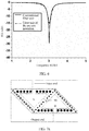
- an operating frequency in a higher order mode of the conventional filter unit is at 2f0, while an operating frequency in a higher order mode of the filter unit of the present invention is at 4f0. Therefore, a parasitic passband of a conventional filter occurs at 2f0, while a parasitic passband of the filter of the present invention occurs nearby 4f0 (f0 is a center frequency of the filter), so as to suppress the parasitic passband.
- a slot whose cross section is circular is provided on a metal covering layer located on a side opposite to the magnetic wall structure, and the two neighboring filter units are connected through magnetic coupling by using the slot.
- the slot has a diameter D and a slot width S, and D/S is less than one tenth wavelength.
- a strip is provided on a metal covering layer located on a side opposite to the electric wall structure, and the two neighboring filter units are connected through electric coupling by using the strip.
- An embodiment of the present invention provides a filter unit.
- the filter unit includes two stacked cavities, where each cavity includes: a dielectric substrate, a first metal covering layer and a second metal covering layer that are disposed on two opposite surfaces of the dielectric substrate, a row of first plated through-holes, a row of second plated through-holes, and a row of third plated through-holes that are provided on the dielectric substrate, and a coupling slot provided on the first metal covering layer, where the first metal covering layer is in a shape of a right triangle; the row of first plated through-holes is parallel to a hypotenuse of the first metal covering layer, and the first plated through-hole runs through the first metal covering layer and the second metal covering layer; the row of second plated through-holes is located outside the first metal covering layer and is parallel to a cathetus of the first metal covering layer, the row of second plated through-holes runs through the second metal covering layer, each of the row of second plated through-holes is connected to a
- the two cavities are stacked to form the filter unit, the two cavities are coupled and connected by using the provided coupling slots to form the filter unit, and only a feeding port needs to be disposed on a hypotenuse of a cavity.
- the filter unit provided in this embodiment includes two cavities that are a first cavity and a second cavity, and the first cavity and the second cavity are coupled and connected by using a coupling slot.
- the metal covering layer may be made of copper.
- FIG. 1 is a schematic structural diagram of a first cavity according to an embodiment of the present invention.
- the first cavity includes a first dielectric substrate 10, and two opposite surfaces of the first dielectric substrate 10 are respectively provided with a first metal covering layer A 20 and a second metal covering layer A 30.
- the first metal covering layer A 20 is in a shape of a right triangle, a shape of the second metal covering layer A 30 is not limited, the first metal covering layer A 20 is provided with first plated through-holes A 40 parallel to a hypotenuse, and the first plated through-holes A 40 run through the first metal covering layer A 20 and the second metal covering layer A 30.
- a row of second plated through-holes A 41 that is located outside the first metal covering layer A 20 and that is parallel to one cathetus of the first metal covering layer A 20 is further provided on the first dielectric substrate 10, and the foregoing being outside the first metal covering layer A 20 means that the first plated through-holes A 40 do not run through the first metal covering layer A 20.
- One end of the second plated through-hole A 41 runs through the first dielectric substrate 10 and the second metal covering layer A 30, the other end is connected to one metal sheet 33, there is a gap between neighboring metal sheets 33, and the metal sheets 33 and the second plated through-holes A 41 form a magnetic wall structure.
- the first dielectric substrate 10 is further provided with a row of third plated through-holes A42 that is located outside the first metal covering layer A 20 and that is parallel to the other hypotenuse of the first metal covering layer A 20, the third plated through-holes A 42 run through the first dielectric substrate 10, and the row of third plated through-holes A 42 form an electric wall structure.
- FIG. 2 shows a structure of a first cavity having a magnetic wall structure and an electric wall structure.
- second plated through-holes A 41 and third plated through-holes A 43 are all located outside a first metal covering layer A 20.
- the second plated through-holes A 41 and the third plated through-holes A 43 runs through the first metal covering layer A 20, and the second plated through-holes A 41 and the third plated through-holes A 43 all run through a first dielectric substrate 10 and a second metal covering layer A 30.
- the second plated through-holes A 41 are connected to metal sheets 33, a row of second plated through-holes A 41 and a row of metal sheets 33 form the magnetic wall structure, and the metal sheets 33 are disposed on the second metal covering layer A 30.
- the metal sheet 33 is a rectangular metal sheet, and a plated through-hole corresponding to the rectangular metal sheet 33 is located at a central location of the rectangular metal sheet 33.
- a row of formed third plated through-holes A 43 is used, and the row of third plated through-holes forms the electric wall structure.
- the first cavity provided in this embodiment is further provided with coupling slots 31, and the coupling slots 31 are provided on the first metal covering layer A 20.
- the coupling slots 31 are parallel to a row of first plated through-holes A 40.
- FIG. 1 it can be learned from FIG. 1 that, during specific disposition, the coupling slots 31 are disposed on a side that departs from a hypotenuse of the second covering layer A 20 and that is of the first plated through-hole A 40 on the second covering layer 20, and a distance from the coupling slot 31 to an edge first plated through-hole A 40 is less than 0.5 mm.
- the distance may be 0.5 mm, 0.4 mm, 0.3 mm, 0.25 mm, 0.2 mm, 0.15 mm, 0.1 mm, 0.05 mm, or another distance.
- the distance from the coupling slot 31 to the edge first plated through-hole A 40 is 0.1 mm.
- the coupling slot 31 has a length L and a width W, and a ratio of the length L to the width W satisfies a condition that L/W falls in between one fourth wavelength and one wavelength, where the wavelength is an operating wavelength of the filter unit.
- a ratio of L/W is: one fourth, one third, one half, two third, one, or the like, so that when being coupled, the first cavity and a second cavity can have a good coupling effect.
- L/W is preferably equal to one half wavelength. Therefore, the first cavity and the second cavity have a good coupling effect.
- one end of the coupling slot 31 facing the magnetic wall structure runs through the first metal covering layer A 20 to form an open end, and a side facing the electric wall structure does not run through the first metal covering layer A 20 to form a closed end.
- a function of run-through or non-run-through of the coupling slot 31 is to affect electromagnetic field distribution inside the filter unit.
- a size of the filter unit of the present invention is greatly reduced, and to achieve this objective, distribution of an electromagnetic field structure inside a conventional filter unit needs to be changed.
- structures of end portions of coupling slots on two cathetuses of the filter unit are not the same, thereby forming different electromagnetic field structures.
- a situation of electromagnetic field distribution on the side is as follows: An electric field is distributed parallel to a cathetus, and strength of the electric field is weaker than strength of a magnetic field, so that the cathetus is characterized by a magnetic wall. 2) The coupling slot does not run through.
- a situation of electromagnetic field distribution on the side is as follows: An electric field is distributed perpendicular to a cathetus, and strength of the electric field is stronger than strength of a magnetic field, so that the cathetus is characterized by an electric wall. Characteristics of the electric wall and the magnetic wall are formed, so that the size of the filter unit is greatly reduced without changing an operating frequency.
- the first cavity further includes two parallel metal slots 32 provided on the first metal covering layer A 20; the two metal slots 32 are separately vertically connected to the coupling slot 31, and divide the coupling slot 31 into two parts, the two metal slots 32 run through the row of first plated through-holes, and the row of first plated through-holes is divided into two parts arranged outside the two metal slots 32; and a microstrip is disposed between two metal slots 32 of one of the cavities.
- the two metal slots 32 run through first plated through-holes A 40 and cut off a row of first plated through-holes A 40, and there is no plated through-hole between the two metal slots 32.
- FIG. 3 and FIG. 4 are separately schematic structural diagrams of second cavities of different structures.
- a structure of a second cavity is similar to a structure of a first cavity, and a unique difference lies only in that a microstrip 73 is connected between two metal slots of the second cavity, and is used as an input end or an output end.
- the microstrip 73 is connected to a metal slot 72.
- a dielectric substrate is a second dielectric substrate 50
- two layer metal covering layers located on the second dielectric substrate 50 are respectively a first metal covering layer B 60 and a second metal covering layer B 70
- a row of plated through-holes located at a hypotenuse is first plated through-holes B 80
- two row of plated through-holes located at cathetuses are respectively second plated through-holes B 81 and third plated through-holes B 82.
- a coupling slot 71, the metal slot 72, and a metal sheet 74 of the second cavity are the same as those of a coupling slot 31, a metal slot 32, and a metal sheet 33 of the first cavity. Details are not described herein again.
- the first metal covering layer B 60 of the second cavity is the same as a first metal covering layer A 20 of the first cavity
- the second metal covering layer B 70 is the same as a second metal covering layer A 30
- the first plated through-hole B 80 and a first plated through-hole A 40 are provided in a same manner
- the second plated through-hole B 81 and a second plated through-hole A 41 have a same structure and are provided in a same manner
- the third plated through-hole B 82 and a third plated through-hole A 43 have a same structure and are provided in a same manner. Details are not described herein again.
- the first cavity and the second cavity are stacked, and the coupling slot of the first cavity and the coupling slot of the second cavity are provided opposite to each other to form a coupling structure. That is, a first copper clad layer of the first cavity comes into contact with a fourth copper clad layer of a third cavity, to complete assembly of the filter unit.
- an embodiment of the present invention further provides a filter.
- the filter includes filter units according to any one of the foregoing items, where two of the filter units are connected to microstrips, one microstrip is used as an input line, the other microstrip is used as an output line, and two neighboring filter units share a magnetic wall structure or an electric wall structure; and when a quantity of the filter units is two, the two filter units are connected through magnetic coupling or electric coupling, or when a quantity of the filter units is more than two, the more than two filter units are connected through alternate coupling of electric coupling and magnetic coupling.
- an operating frequency in a higher order mode of the conventional filter unit is at 2f0, while an operating frequency in a higher order mode of the filter unit of the present invention is at 4f0. Therefore, a parasitic passband of a conventional filter occurs at 2f0, while a parasitic passband of the filter of the present invention occurs nearby 4f0 (f0 is a center frequency of the filter), so as to suppress the parasitic passband.
- a quantity of the filter units in the filter is at least two, and when two filter units are used, the two filter units are respectively a filter unit A and a filter unit B.
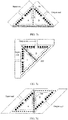
- FIG. 7a to FIG. 7d show that two filter units share an electric wall structure, and the two filter units are electrically coupled by using a strip.
- FIG. 7c and FIG. 7d show that two filter units share a magnetic wall structure, and the two filter units are coupled by using a slot.
- a slot 100 whose cross section is circular is provided on a metal covering layer located on a side opposite to the magnetic wall structure, and the two neighboring filter units are connected through magnetic coupling by using the slot 100.
- the slot 100 has a diameter D and a slot width S, and D/S is less than one tenth wavelength.
- a strip 90 is provided on a metal covering layer located on a side opposite to the electric wall structure, and the two neighboring filter units are connected through electric coupling by using the strip 90.
- letters A, B, C, and D represent four filter units.
- a filter unit A and a filter unit D are respectively connected to a microstrip 73 at an input end and a microstrip 73 at an output end.
- the filter unit A and the filter unit B are cascaded in an electric coupling manner by using a strip 90
- the filter unit C and the filter unit D are cascaded in an electric coupling manner by using a strip 90.
- the filter unit B and the filter unit C are cascaded in a magnetic coupling manner by using circular coupling slots 100.
- the circular coupling slots 100 in magnetic coupling are symmetrically distributed at a second metal covering layer and a fourth metal covering layer, and are located at a middle location of a magnetic wall of the filter units.
- the strips 90 in electric coupling are located at a first metal covering layer and a third metal covering layer, and the strips 90 in electric coupling are connected to the metal covering layers.
- an operating frequency in a higher order mode of the conventional filter unit is at 2f0, while an operating frequency in a higher order mode of the filter unit of the present invention is at 4f0. Therefore, a parasitic passband of a conventional filter occurs at 2f0, while a parasitic passband of the filter of the present invention occurs nearby 4f0 (f0 is a center frequency of the filter), so as to suppress the parasitic passband.
Landscapes
- Control Of Motors That Do Not Use Commutators (AREA)
Applications Claiming Priority (1)
| Application Number | Priority Date | Filing Date | Title |
|---|---|---|---|
| PCT/CN2016/072804 WO2017128298A1 (fr) | 2016-01-29 | 2016-01-29 | Unité de filtre et filtre |
Publications (3)
| Publication Number | Publication Date |
|---|---|
| EP3367496A1 true EP3367496A1 (fr) | 2018-08-29 |
| EP3367496A4 EP3367496A4 (fr) | 2018-12-26 |
| EP3367496B1 EP3367496B1 (fr) | 2020-10-07 |
Family
ID=59397126
Family Applications (1)
| Application Number | Title | Priority Date | Filing Date |
|---|---|---|---|
| EP16887182.0A Active EP3367496B1 (fr) | 2016-01-29 | 2016-01-29 | Unité de filtre et filtre |
Country Status (4)
| Country | Link |
|---|---|
| US (1) | US10622693B2 (fr) |
| EP (1) | EP3367496B1 (fr) |
| CN (1) | CN108140925B (fr) |
| WO (1) | WO2017128298A1 (fr) |
Families Citing this family (10)
| Publication number | Priority date | Publication date | Assignee | Title |
|---|---|---|---|---|
| CN108428984A (zh) * | 2018-03-15 | 2018-08-21 | 南京邮电大学 | 基于直角三角形基片集成谐振腔的带通滤波器 |
| CN109638397B (zh) * | 2018-11-05 | 2021-02-02 | 西安电子科技大学 | 一种双层堆叠式微波带通滤波器 |
| CN111446532B (zh) * | 2020-03-26 | 2021-01-05 | 成都频岢微电子有限公司 | 一种基于基片集成波导的同轴谐振腔及其滤波器 |
| CN111463525B (zh) * | 2020-04-20 | 2021-04-27 | 南京邮电大学 | 基于共面波导的小型化的三阶sd-hmsiw带通滤波器 |
| CN112886160B (zh) * | 2021-01-14 | 2021-11-30 | 中国电子科技集团公司第五十五研究所 | 一种基于硅基mems工艺的紧凑型基片集成波导滤波器 |
| CN113193317B (zh) * | 2021-05-14 | 2022-05-03 | 南京智能高端装备产业研究院有限公司 | 一种采用单层圆形贴片的双通带功分滤波器 |
| CN114865255B (zh) * | 2022-07-07 | 2022-09-13 | 微网优联科技(成都)有限公司 | 一种半模基片集成波导滤波器 |
| CN116345093A (zh) * | 2023-04-04 | 2023-06-27 | 电子科技大学 | 一种x波段siw非整数维度超结构滤波器及其设计方法 |
| CN116706480B (zh) * | 2023-07-21 | 2024-06-21 | 南京邮电大学 | 一种紧凑的高选择性基片集成波导三角腔宽阻带滤波器 |
| CN116759779B (zh) * | 2023-08-22 | 2023-11-10 | 安徽蓝讯通信科技有限公司 | 一种5g毫米波滤波功分模块 |
Family Cites Families (6)
| Publication number | Priority date | Publication date | Assignee | Title |
|---|---|---|---|---|
| JP3839410B2 (ja) | 2003-02-12 | 2006-11-01 | Tdk株式会社 | フィルタおよび共振器の配置方法 |
| US8309925B2 (en) * | 2009-09-17 | 2012-11-13 | William Marsh Rice University | Resonant cavity integrated into a waveguide for terahertz sensing |
| DE102010019525B4 (de) * | 2010-05-06 | 2012-06-21 | Tutech Innovation Gmbh | Nahfeldsensor zur lokalen Messung von dielektrischen Eigenschaften |
| CN102354790B (zh) * | 2011-10-25 | 2014-04-09 | 电子科技大学 | 高度小型化的基片集成波导谐振器 |
| KR101378477B1 (ko) * | 2013-03-22 | 2014-03-28 | 중앙대학교 산학협력단 | 기판 집적형 도파관 안테나 |
| CN105006613A (zh) * | 2015-07-03 | 2015-10-28 | 中国矿业大学 | 一种椭圆缺陷结构四分之一模基片集成波导带通滤波器 |
-
2016
- 2016-01-29 CN CN201680058439.7A patent/CN108140925B/zh active Active
- 2016-01-29 WO PCT/CN2016/072804 patent/WO2017128298A1/fr not_active Ceased
- 2016-01-29 EP EP16887182.0A patent/EP3367496B1/fr active Active
-
2018
- 2018-05-15 US US15/980,646 patent/US10622693B2/en active Active
Also Published As
| Publication number | Publication date |
|---|---|
| EP3367496B1 (fr) | 2020-10-07 |
| US10622693B2 (en) | 2020-04-14 |
| EP3367496A4 (fr) | 2018-12-26 |
| CN108140925A (zh) | 2018-06-08 |
| US20180261901A1 (en) | 2018-09-13 |
| WO2017128298A1 (fr) | 2017-08-03 |
| CN108140925B (zh) | 2019-11-19 |
Similar Documents
| Publication | Publication Date | Title |
|---|---|---|
| EP3367496A1 (fr) | Unité de filtre et filtre | |
| US8258897B2 (en) | Ground structures in resonators for planar and folded distributed electromagnetic wave filters | |
| US7902944B2 (en) | Stacked resonator | |
| CN107819180B (zh) | 基片集成波导器件与基片集成波导滤波器 | |
| CN114245955B (zh) | 电介质谐振器、电介质滤波器、以及多工器 | |
| CN110797614B (zh) | 一种具有高次模抑制的小型化基片集成波导滤波器 | |
| CN105226355B (zh) | 高寄生通带抑制四分之一模基片集成波导频率选择表面 | |
| CN112952322A (zh) | 基于折叠基片集成波导谐振腔的双模带通滤波器 | |
| CN108428984A (zh) | 基于直角三角形基片集成谐振腔的带通滤波器 | |
| JP2005260570A (ja) | マイクロストリップ線路導波管変換器 | |
| CN106299560A (zh) | 一种高选择性宽带功分滤波器 | |
| JPH09252206A (ja) | 誘電体フィルタ | |
| CN105789786B (zh) | 基于基片集成波导互补开口谐振环的低插损宽带滤波器 | |
| CN106549201B (zh) | 一种由具有插指端口的h型微带谐振器组成的滤波器 | |
| Zhu et al. | Double-layer SIW filters with higher-order mode suppression | |
| CN114865255B (zh) | 一种半模基片集成波导滤波器 | |
| US10673111B2 (en) | Filtering unit and filter | |
| JP5163654B2 (ja) | ストリップラインフィルタおよびその製造方法 | |
| JP5481293B2 (ja) | 分布定数線路型バンドパスフィルタ | |
| US20120032760A1 (en) | Compact planar resonators with z-axis folding | |
| CN114389002A (zh) | 加载互补阶梯折叠开口环的siw滤波功分器及设计方法 | |
| CN205452493U (zh) | 基于新型开口谐振环结构的共面波导带通滤波器 | |
| CN119994425B (zh) | 基于多层金属薄片波导的带通滤波器 | |
| CN221379694U (zh) | 一种拓扑结构及具有陷波特性的宽带带通滤波器 | |
| CN221176618U (zh) | 一种拓扑结构及五阶小型化宽通带滤波器 |
Legal Events
| Date | Code | Title | Description |
|---|---|---|---|
| STAA | Information on the status of an ep patent application or granted ep patent |
Free format text: STATUS: THE INTERNATIONAL PUBLICATION HAS BEEN MADE |
|
| PUAI | Public reference made under article 153(3) epc to a published international application that has entered the european phase |
Free format text: ORIGINAL CODE: 0009012 |
|
| STAA | Information on the status of an ep patent application or granted ep patent |
Free format text: STATUS: REQUEST FOR EXAMINATION WAS MADE |
|
| 17P | Request for examination filed |
Effective date: 20180516 |
|
| AK | Designated contracting states |
Kind code of ref document: A1 Designated state(s): AL AT BE BG CH CY CZ DE DK EE ES FI FR GB GR HR HU IE IS IT LI LT LU LV MC MK MT NL NO PL PT RO RS SE SI SK SM TR |
|
| AX | Request for extension of the european patent |
Extension state: BA ME |
|
| A4 | Supplementary search report drawn up and despatched |
Effective date: 20181122 |
|
| RIC1 | Information provided on ipc code assigned before grant |
Ipc: H01P 1/208 20060101ALI20181116BHEP Ipc: H01P 7/06 20060101AFI20181116BHEP |
|
| DAV | Request for validation of the european patent (deleted) | ||
| DAX | Request for extension of the european patent (deleted) | ||
| REG | Reference to a national code |
Ref country code: DE Ref legal event code: R079 Ref document number: 602016045627 Country of ref document: DE Free format text: PREVIOUS MAIN CLASS: H01P0007000000 Ipc: H01P0007060000 |
|
| RIC1 | Information provided on ipc code assigned before grant |
Ipc: H01P 1/208 20060101ALI20200310BHEP Ipc: H01P 7/06 20060101AFI20200310BHEP |
|
| GRAP | Despatch of communication of intention to grant a patent |
Free format text: ORIGINAL CODE: EPIDOSNIGR1 |
|
| STAA | Information on the status of an ep patent application or granted ep patent |
Free format text: STATUS: GRANT OF PATENT IS INTENDED |
|
| INTG | Intention to grant announced |
Effective date: 20200429 |
|
| GRAS | Grant fee paid |
Free format text: ORIGINAL CODE: EPIDOSNIGR3 |
|
| GRAA | (expected) grant |
Free format text: ORIGINAL CODE: 0009210 |
|
| STAA | Information on the status of an ep patent application or granted ep patent |
Free format text: STATUS: THE PATENT HAS BEEN GRANTED |
|
| AK | Designated contracting states |
Kind code of ref document: B1 Designated state(s): AL AT BE BG CH CY CZ DE DK EE ES FI FR GB GR HR HU IE IS IT LI LT LU LV MC MK MT NL NO PL PT RO RS SE SI SK SM TR |
|
| REG | Reference to a national code |
Ref country code: GB Ref legal event code: FG4D |
|
| REG | Reference to a national code |
Ref country code: AT Ref legal event code: REF Ref document number: 1322134 Country of ref document: AT Kind code of ref document: T Effective date: 20201015 Ref country code: CH Ref legal event code: EP |
|
| REG | Reference to a national code |
Ref country code: IE Ref legal event code: FG4D |
|
| REG | Reference to a national code |
Ref country code: DE Ref legal event code: R096 Ref document number: 602016045627 Country of ref document: DE |
|
| REG | Reference to a national code |
Ref country code: NL Ref legal event code: MP Effective date: 20201007 |
|
| REG | Reference to a national code |
Ref country code: AT Ref legal event code: MK05 Ref document number: 1322134 Country of ref document: AT Kind code of ref document: T Effective date: 20201007 |
|
| PG25 | Lapsed in a contracting state [announced via postgrant information from national office to epo] |
Ref country code: NO Free format text: LAPSE BECAUSE OF FAILURE TO SUBMIT A TRANSLATION OF THE DESCRIPTION OR TO PAY THE FEE WITHIN THE PRESCRIBED TIME-LIMIT Effective date: 20210107 Ref country code: RS Free format text: LAPSE BECAUSE OF FAILURE TO SUBMIT A TRANSLATION OF THE DESCRIPTION OR TO PAY THE FEE WITHIN THE PRESCRIBED TIME-LIMIT Effective date: 20201007 Ref country code: PT Free format text: LAPSE BECAUSE OF FAILURE TO SUBMIT A TRANSLATION OF THE DESCRIPTION OR TO PAY THE FEE WITHIN THE PRESCRIBED TIME-LIMIT Effective date: 20210208 Ref country code: GR Free format text: LAPSE BECAUSE OF FAILURE TO SUBMIT A TRANSLATION OF THE DESCRIPTION OR TO PAY THE FEE WITHIN THE PRESCRIBED TIME-LIMIT Effective date: 20210108 Ref country code: FI Free format text: LAPSE BECAUSE OF FAILURE TO SUBMIT A TRANSLATION OF THE DESCRIPTION OR TO PAY THE FEE WITHIN THE PRESCRIBED TIME-LIMIT Effective date: 20201007 |
|
| REG | Reference to a national code |
Ref country code: LT Ref legal event code: MG4D |
|
| PG25 | Lapsed in a contracting state [announced via postgrant information from national office to epo] |
Ref country code: SE Free format text: LAPSE BECAUSE OF FAILURE TO SUBMIT A TRANSLATION OF THE DESCRIPTION OR TO PAY THE FEE WITHIN THE PRESCRIBED TIME-LIMIT Effective date: 20201007 Ref country code: ES Free format text: LAPSE BECAUSE OF FAILURE TO SUBMIT A TRANSLATION OF THE DESCRIPTION OR TO PAY THE FEE WITHIN THE PRESCRIBED TIME-LIMIT Effective date: 20201007 Ref country code: AT Free format text: LAPSE BECAUSE OF FAILURE TO SUBMIT A TRANSLATION OF THE DESCRIPTION OR TO PAY THE FEE WITHIN THE PRESCRIBED TIME-LIMIT Effective date: 20201007 Ref country code: BG Free format text: LAPSE BECAUSE OF FAILURE TO SUBMIT A TRANSLATION OF THE DESCRIPTION OR TO PAY THE FEE WITHIN THE PRESCRIBED TIME-LIMIT Effective date: 20210107 Ref country code: PL Free format text: LAPSE BECAUSE OF FAILURE TO SUBMIT A TRANSLATION OF THE DESCRIPTION OR TO PAY THE FEE WITHIN THE PRESCRIBED TIME-LIMIT Effective date: 20201007 Ref country code: IS Free format text: LAPSE BECAUSE OF FAILURE TO SUBMIT A TRANSLATION OF THE DESCRIPTION OR TO PAY THE FEE WITHIN THE PRESCRIBED TIME-LIMIT Effective date: 20210207 Ref country code: LV Free format text: LAPSE BECAUSE OF FAILURE TO SUBMIT A TRANSLATION OF THE DESCRIPTION OR TO PAY THE FEE WITHIN THE PRESCRIBED TIME-LIMIT Effective date: 20201007 |
|
| PG25 | Lapsed in a contracting state [announced via postgrant information from national office to epo] |
Ref country code: NL Free format text: LAPSE BECAUSE OF FAILURE TO SUBMIT A TRANSLATION OF THE DESCRIPTION OR TO PAY THE FEE WITHIN THE PRESCRIBED TIME-LIMIT Effective date: 20201007 Ref country code: HR Free format text: LAPSE BECAUSE OF FAILURE TO SUBMIT A TRANSLATION OF THE DESCRIPTION OR TO PAY THE FEE WITHIN THE PRESCRIBED TIME-LIMIT Effective date: 20201007 |
|
| REG | Reference to a national code |
Ref country code: DE Ref legal event code: R097 Ref document number: 602016045627 Country of ref document: DE |
|
| PG25 | Lapsed in a contracting state [announced via postgrant information from national office to epo] |
Ref country code: SM Free format text: LAPSE BECAUSE OF FAILURE TO SUBMIT A TRANSLATION OF THE DESCRIPTION OR TO PAY THE FEE WITHIN THE PRESCRIBED TIME-LIMIT Effective date: 20201007 Ref country code: LT Free format text: LAPSE BECAUSE OF FAILURE TO SUBMIT A TRANSLATION OF THE DESCRIPTION OR TO PAY THE FEE WITHIN THE PRESCRIBED TIME-LIMIT Effective date: 20201007 Ref country code: EE Free format text: LAPSE BECAUSE OF FAILURE TO SUBMIT A TRANSLATION OF THE DESCRIPTION OR TO PAY THE FEE WITHIN THE PRESCRIBED TIME-LIMIT Effective date: 20201007 Ref country code: CZ Free format text: LAPSE BECAUSE OF FAILURE TO SUBMIT A TRANSLATION OF THE DESCRIPTION OR TO PAY THE FEE WITHIN THE PRESCRIBED TIME-LIMIT Effective date: 20201007 Ref country code: RO Free format text: LAPSE BECAUSE OF FAILURE TO SUBMIT A TRANSLATION OF THE DESCRIPTION OR TO PAY THE FEE WITHIN THE PRESCRIBED TIME-LIMIT Effective date: 20201007 Ref country code: SK Free format text: LAPSE BECAUSE OF FAILURE TO SUBMIT A TRANSLATION OF THE DESCRIPTION OR TO PAY THE FEE WITHIN THE PRESCRIBED TIME-LIMIT Effective date: 20201007 |
|
| PLBE | No opposition filed within time limit |
Free format text: ORIGINAL CODE: 0009261 |
|
| STAA | Information on the status of an ep patent application or granted ep patent |
Free format text: STATUS: NO OPPOSITION FILED WITHIN TIME LIMIT |
|
| PG25 | Lapsed in a contracting state [announced via postgrant information from national office to epo] |
Ref country code: DK Free format text: LAPSE BECAUSE OF FAILURE TO SUBMIT A TRANSLATION OF THE DESCRIPTION OR TO PAY THE FEE WITHIN THE PRESCRIBED TIME-LIMIT Effective date: 20201007 Ref country code: MC Free format text: LAPSE BECAUSE OF FAILURE TO SUBMIT A TRANSLATION OF THE DESCRIPTION OR TO PAY THE FEE WITHIN THE PRESCRIBED TIME-LIMIT Effective date: 20201007 |
|
| REG | Reference to a national code |
Ref country code: CH Ref legal event code: PL |
|
| 26N | No opposition filed |
Effective date: 20210708 |
|
| PG25 | Lapsed in a contracting state [announced via postgrant information from national office to epo] |
Ref country code: LU Free format text: LAPSE BECAUSE OF NON-PAYMENT OF DUE FEES Effective date: 20210129 |
|
| REG | Reference to a national code |
Ref country code: BE Ref legal event code: MM Effective date: 20210131 |
|
| PG25 | Lapsed in a contracting state [announced via postgrant information from national office to epo] |
Ref country code: AL Free format text: LAPSE BECAUSE OF FAILURE TO SUBMIT A TRANSLATION OF THE DESCRIPTION OR TO PAY THE FEE WITHIN THE PRESCRIBED TIME-LIMIT Effective date: 20201007 Ref country code: IT Free format text: LAPSE BECAUSE OF FAILURE TO SUBMIT A TRANSLATION OF THE DESCRIPTION OR TO PAY THE FEE WITHIN THE PRESCRIBED TIME-LIMIT Effective date: 20201007 Ref country code: FR Free format text: LAPSE BECAUSE OF NON-PAYMENT OF DUE FEES Effective date: 20210131 |
|
| PG25 | Lapsed in a contracting state [announced via postgrant information from national office to epo] |
Ref country code: SI Free format text: LAPSE BECAUSE OF FAILURE TO SUBMIT A TRANSLATION OF THE DESCRIPTION OR TO PAY THE FEE WITHIN THE PRESCRIBED TIME-LIMIT Effective date: 20201007 Ref country code: CH Free format text: LAPSE BECAUSE OF NON-PAYMENT OF DUE FEES Effective date: 20210131 Ref country code: LI Free format text: LAPSE BECAUSE OF NON-PAYMENT OF DUE FEES Effective date: 20210131 |
|
| PG25 | Lapsed in a contracting state [announced via postgrant information from national office to epo] |
Ref country code: IE Free format text: LAPSE BECAUSE OF NON-PAYMENT OF DUE FEES Effective date: 20210129 |
|
| PG25 | Lapsed in a contracting state [announced via postgrant information from national office to epo] |
Ref country code: IS Free format text: LAPSE BECAUSE OF FAILURE TO SUBMIT A TRANSLATION OF THE DESCRIPTION OR TO PAY THE FEE WITHIN THE PRESCRIBED TIME-LIMIT Effective date: 20210207 |
|
| PG25 | Lapsed in a contracting state [announced via postgrant information from national office to epo] |
Ref country code: BE Free format text: LAPSE BECAUSE OF NON-PAYMENT OF DUE FEES Effective date: 20210131 |
|
| PG25 | Lapsed in a contracting state [announced via postgrant information from national office to epo] |
Ref country code: CY Free format text: LAPSE BECAUSE OF FAILURE TO SUBMIT A TRANSLATION OF THE DESCRIPTION OR TO PAY THE FEE WITHIN THE PRESCRIBED TIME-LIMIT Effective date: 20201007 |
|
| PG25 | Lapsed in a contracting state [announced via postgrant information from national office to epo] |
Ref country code: HU Free format text: LAPSE BECAUSE OF FAILURE TO SUBMIT A TRANSLATION OF THE DESCRIPTION OR TO PAY THE FEE WITHIN THE PRESCRIBED TIME-LIMIT; INVALID AB INITIO Effective date: 20160129 |
|
| PG25 | Lapsed in a contracting state [announced via postgrant information from national office to epo] |
Ref country code: MK Free format text: LAPSE BECAUSE OF FAILURE TO SUBMIT A TRANSLATION OF THE DESCRIPTION OR TO PAY THE FEE WITHIN THE PRESCRIBED TIME-LIMIT Effective date: 20201007 |
|
| PG25 | Lapsed in a contracting state [announced via postgrant information from national office to epo] |
Ref country code: TR Free format text: LAPSE BECAUSE OF FAILURE TO SUBMIT A TRANSLATION OF THE DESCRIPTION OR TO PAY THE FEE WITHIN THE PRESCRIBED TIME-LIMIT Effective date: 20201007 |
|
| PG25 | Lapsed in a contracting state [announced via postgrant information from national office to epo] |
Ref country code: MT Free format text: LAPSE BECAUSE OF FAILURE TO SUBMIT A TRANSLATION OF THE DESCRIPTION OR TO PAY THE FEE WITHIN THE PRESCRIBED TIME-LIMIT Effective date: 20201007 |
|
| PGFP | Annual fee paid to national office [announced via postgrant information from national office to epo] |
Ref country code: GB Payment date: 20251211 Year of fee payment: 11 |
|
| PGFP | Annual fee paid to national office [announced via postgrant information from national office to epo] |
Ref country code: DE Payment date: 20251203 Year of fee payment: 11 |