EP3369095B1 - Flächeneffizienter paralleltestdatenpfad für eingebettete speicher - Google Patents
Flächeneffizienter paralleltestdatenpfad für eingebettete speicher Download PDFInfo
- Publication number
- EP3369095B1 EP3369095B1 EP16861067.3A EP16861067A EP3369095B1 EP 3369095 B1 EP3369095 B1 EP 3369095B1 EP 16861067 A EP16861067 A EP 16861067A EP 3369095 B1 EP3369095 B1 EP 3369095B1
- Authority
- EP
- European Patent Office
- Prior art keywords
- memories
- group
- local
- delay
- memory
- Prior art date
- Legal status (The legal status is an assumption and is not a legal conclusion. Google has not performed a legal analysis and makes no representation as to the accuracy of the status listed.)
- Active
Links
Images



Classifications
-
- G—PHYSICS
- G11—INFORMATION STORAGE
- G11C—STATIC STORES
- G11C29/00—Checking stores for correct operation ; Subsequent repair; Testing stores during standby or offline operation
- G11C29/04—Detection or location of defective memory elements, e.g. cell constructio details, timing of test signals
- G11C29/08—Functional testing, e.g. testing during refresh, power-on self testing [POST] or distributed testing
- G11C29/12—Built-in arrangements for testing, e.g. built-in self testing [BIST] or interconnection details
-
- G—PHYSICS
- G11—INFORMATION STORAGE
- G11C—STATIC STORES
- G11C29/00—Checking stores for correct operation ; Subsequent repair; Testing stores during standby or offline operation
- G11C29/04—Detection or location of defective memory elements, e.g. cell constructio details, timing of test signals
- G11C29/08—Functional testing, e.g. testing during refresh, power-on self testing [POST] or distributed testing
- G11C29/12—Built-in arrangements for testing, e.g. built-in self testing [BIST] or interconnection details
- G11C29/38—Response verification devices
-
- G—PHYSICS
- G06—COMPUTING OR CALCULATING; COUNTING
- G06F—ELECTRIC DIGITAL DATA PROCESSING
- G06F15/00—Digital computers in general; Data processing equipment in general
- G06F15/76—Architectures of general purpose stored program computers
- G06F15/78—Architectures of general purpose stored program computers comprising a single central processing unit
- G06F15/7807—System on chip, i.e. computer system on a single chip; System in package, i.e. computer system on one or more chips in a single package
-
- G—PHYSICS
- G11—INFORMATION STORAGE
- G11C—STATIC STORES
- G11C29/00—Checking stores for correct operation ; Subsequent repair; Testing stores during standby or offline operation
- G11C29/04—Detection or location of defective memory elements, e.g. cell constructio details, timing of test signals
- G11C29/08—Functional testing, e.g. testing during refresh, power-on self testing [POST] or distributed testing
- G11C29/12—Built-in arrangements for testing, e.g. built-in self testing [BIST] or interconnection details
- G11C29/38—Response verification devices
- G11C29/40—Response verification devices using compression techniques
-
- G—PHYSICS
- G11—INFORMATION STORAGE
- G11C—STATIC STORES
- G11C29/00—Checking stores for correct operation ; Subsequent repair; Testing stores during standby or offline operation
- G11C29/04—Detection or location of defective memory elements, e.g. cell constructio details, timing of test signals
- G11C2029/0401—Detection or location of defective memory elements, e.g. cell constructio details, timing of test signals in embedded memories
-
- G—PHYSICS
- G11—INFORMATION STORAGE
- G11C—STATIC STORES
- G11C29/00—Checking stores for correct operation ; Subsequent repair; Testing stores during standby or offline operation
- G11C29/04—Detection or location of defective memory elements, e.g. cell constructio details, timing of test signals
- G11C29/08—Functional testing, e.g. testing during refresh, power-on self testing [POST] or distributed testing
- G11C29/12—Built-in arrangements for testing, e.g. built-in self testing [BIST] or interconnection details
- G11C29/18—Address generation devices; Devices for accessing memories, e.g. details of addressing circuits
- G11C29/26—Accessing multiple arrays
- G11C2029/2602—Concurrent test
Definitions
- This relates generally to integrated circuit testing, and more particularly to testing of embedded memories in large-scale integrated circuits.
- SoC system on a chip
- Typical modern SoC architectures include one or more processor “cores” that perform the digital computer functions of retrieving executable instructions from memory, performing arithmetic and logical operations on digital data retrieved from memory, and storing the results of those operations in memory.
- Other digital, analog, mixed-signal, or even RF functions may also be integrated into the SoC for acquiring and outputting the data processed by the processor cores.
- memory resources are typically distributed throughout the typical modern SoC device. These memory resources can include both volatile and non-volatile memory. This distributed memory architecture results in memory resources being physically and electrically (or logically) proximate to the processing function that will be accessing it, but may be physically and logically remote from other similar memory of the same type. For example, the deployment of local memory resources will minimize the traffic over the system bus, which reduces the likelihood of bus contention and undesirable latency, and also reduces access time and memory management overhead. The number of memory arrays implemented throughout a modern large-scale SoC devices can be quite large, numbering into the hundreds in some cases.
- SoC devices typically include internal test circuitry ("built-in self-test,” or “BIST,” circuitry) that executes a self-test operation for the device upon power-up or reset. BIST may also be involved in the testing of memory, both at the time of manufacture and also on power-up.
- BIST memory test techniques can include the placement of hardwired logic in the SoC, for implementing memory test algorithms developed at the time of circuit design. However, at that early stage of the process, a determination of the particular tests to be performed may not be feasible.
- Another conventional BIST approach is to use the central processing unit of the SoC itself to perform the memory test. But this approach can be limited, because not all embedded memory arrays in the device may be visible to the CPU, and are thus not testable by the CPU.
- Direct memory access (DMA) techniques for providing external access to embedded memories are also known, but typically are unable to access the memory at its full operating speed.
- the pBIST circuitry includes a general purpose test controller that is programmed by a set of instructions to produce test conditions for the various internal and embedded functions of the device, and to receive and log the responses of those functions to those test conditions.
- these operations include the writing of the desired data pattern to an embedded memory, and then addressing the memory to retrieve and compare the stored data to the expected data.
- the BIST data path over which the data are communicated during memory test is a separate and independent data path from that by which the embedded memories are accessed in normal operation of the SoC.
- this parallel test is implemented by multiple BIST controllers that simultaneously execute a test of an associated embedded memory.
- the provision of multiple BIST controllers multiplies the chip area required for the BIST test logic and data paths, forcing a trade-off between chip area and test time.
- Conventional pBIST architectures such as described in the above mentioned U.S. Patent No. 7,324,392 , include a BIST controller that is shared by multiple memories of similar memory type (e.g., single-port, double-port).
- the shared BIST controller generates the test pattern to be written to the memories, and also the expected response from the memories when read.
- Each memory has a local comparator that compares the data read from its memory during the test with the expected data from the shared BIST controller, and forwards the results to the shared BIST controller.
- this conventional arrangement includes a local response delay generator that aligns the expected data to account for access latency for that particular memory, and a local comparator that compares the delayed expected data with the data read from that particular memory and generates a pass/fail signature accordingly.
- FIG 1 illustrates an example of the architecture of a BIST memory test data path in a conventional SoC, in which shared BIST controller 10 supports the parallel test of memories 15 in a manner such as described in the above-incorporated U.S. Patent No. 7,324,392 .
- This test data path is separate and independent from the data path by which memories 15 are accessed in normal operation, which is not shown in FIG 1 for the sake of clarity.
- BIST controller 10 communicates with each memory 15 through one or more pipeline delay stages 12, in combination with an instance of local response delay generator 14 that is dedicated to that embedded memory 15.
- BIST controller 10 may be one of multiple such BIST controllers within the SoC.
- a given BIST controller 10 is typically associated with memories 15 that are of a common type (e.g., single-port, double-port), considering that BIST controller 10 generates the particular test data pattern to be applied to its associated memories 15; as such, if the SoC includes multiple memory types, multiple BIST controllers 10 and associated data paths may be present.
- the data pattern generated by BIST controller 10 is applied directly to memories 15, after passing through the pipeline delay stages 12, but these data are not delayed by local response delay generators 14.
- pipeline delays 12 and each local response delay generator 14 delay the expected data response communicated from BIST controller 10 before application to the instance of local comparator 16 with which that local response delay generator 14 is associated.
- Local comparator 16 compares that delayed expected data response with the data read from its associated memory 15 during the memory test, and generates a pass/fail signature based on the results of that comparison.
- the pass/fail signatures generated by comparators 16 are communicated back to BIST controller 10, such as by parallel test data comparator 17 function, which produces an overall pass/fail signature for those memories 15 that were tested in parallel.
- instances of pipeline delays 12 may be shared by embedded memories 15 that are generally in the vicinity of one another.
- pipeline delay 120 is shared by all embedded memories 15 shown in FIG 1
- pipeline delay 121 is shared by embedded memories 15 of group 181 that are in the general vicinity of one another
- pipeline delay 122 is shared by embedded memories 15 in group 182 that are in the general vicinity of one another.
- Each of pipeline delays 12 essentially operate as one or more clocked buffer stages for the data communicated by BIST controller 10, such that a data word applied at the input of an instance of pipeline delay 12 will appear at its output after a delay of x clock cycles, where x is the number of buffer stages in that pipeline delay 12.
- Each local response delay generator 14 is similarly constructed, and operates to delay the expected data it receives by one or more clock cycles, in order to align it with the memory access latency of its associated embedded memory 15.
- the memory comprises a plurality of RAM arrays which are simultaneously tested and wherein their test response is compared in a comparator with a test response of a pseudo memory.
- the pseudo memory functions to delay the test pattern corresponding to the delay introduced by the RAM arrays. The document does not disclose a second pseudo memory for a second group of tested memories.
- a BIST controller generates test data patterns to be applied to embedded memories through a BIST data path.
- Each embedded memory is coupled to a dedicated local comparator that compares data read from the memory during test with an expected data response forwarded from the BIST controller.
- the local comparators associated with a group of the memories to be tested in parallel receive the expected data response in parallel from a local response delay generator that is shared among the group.
- Example embodiments provide a built-in self-test (BIST) architecture for the parallel test of distributed memories in a large-scale integrated circuit can be implemented with reduced chip area.
- BIST built-in self-test
- such embodiments provide such a BIST parallel memory test architecture that is suitable for implementation in system-on-a-chip (SoC) devices.
- SoC system-on-a-chip
- example embodiments provide such a BIST parallel memory test architecture that enables parallel test of embedded memories at full operating speed.
- inventions described in this specification are implemented into a large-scale integrated circuit device including a number of computing and other operational functions, such as those integrated circuits commonly referred to as a "system-on-a-chip” or “SoC", because such implementation is particularly advantageous in that context.
- SoC system-on-a-chip
- example embodiments may be beneficially applied to in other applications, such as any type of integrated circuit in which a number of memory arrays are embedded at various locations within the device.
- FIG 2 illustrates, in block diagram form, the generalized architecture of SoC 400 constructed according to these embodiments.
- programmable logic serving as the central processing unit (CPU) of SoC 400 is provided by CPU 430 (e.g., microprocessor), such as an OMAP processor available from Texas Instruments Incorporated.
- SoC 400 may be constructed to include multiple CPUs 430, which may be of the same type as one another or which may be processors of other types such as generic programmable processors, digital signal processors (DSPs) or other application-specific or customized logic, including fixed sequence generators, as appropriate for the particular function of SoC 400.
- DSPs digital signal processors
- Memory resources in SoC 400 are provided by non-volatile flash memory 410, read-only memory (ROM) 411, and random access memory 412, a portion of each of which is accessible to CPU 430 through address bus MAB and data bus MDB.
- the flash memory 410, ROM 411 and RAM 412 are shown in FIG 2 as unitary blocks, but these memory resources may alternatively be implemented as multiple memory blocks or arrays.
- these memory instances may be implemented by any one or more of a number of memory cell types and arrangements, including static RAM (SRAM), dynamic RAM (DRAM), and ferroelectric memory (FRAM).
- SRAM static RAM
- DRAM dynamic RAM
- FRAM ferroelectric memory
- individual instances of memory resources may have any one of a number of access architectures, including single-port and double-port access types.
- peripheral functions may be also coupled to buses MAB, MDB, in order to be accessible to CPU 430 and one another.
- these peripherals include various signal processing functions, such as analog-to-digital (ADC) and digital-to-analog (DAC) converters, communications ports, timers, a "brownout” protection function, and serial and other interface functions.
- ADC analog-to-digital
- DAC digital-to-analog
- These various peripheral functions may be within the address space of SoC 400, as suggested by their accessibility via buses MAB, MDB; alternatively, one or more of these or other functions may be accessible to CPU 430 directly or via other functional circuitry.
- SoC 400 Security features may also be implemented within SoC 400, such as by secure state machine 448 in combination with stored security parameters in secure flash memory 440 and secure tag hardware 446, in order to execute features such as preventing data reads or writes to areas of memory that are specified to be secure areas unless a secure mode is enabled.
- SoC 400 also includes other functions, such as its clock system, emulation system 420 and JTAG interface 421 for debug and emulation.
- SoC 400 may include additional or alternative functions to those shown in FIG 2 , or may have its functions arranged according to a different architecture from that shown in FIG 1 .
- SoC 400 may themselves include local memory resources that are not directly accessible to CPU 430.
- digital functions such as the various interfaces, state machines (e.g., SM 448) and timers, can include blocks of RAM for data storage, or even flash memory or ROM for storage of configuration data or program instructions.
- these memory resources may collectively, if not individually, occupy significant chip area in SoC 400.
- functional testing of these memory resources is important, even though they may not be directly accessible to CPU 430 via buses MAB, MDB or otherwise.
- CPU 430 itself may also include local memory resources, such as one or more levels of cache memory.
- the various memory resources and other functions in the architecture of SoC 400 may not be physically implemented in the arrangement shown in FIG 2 , but may instead be placed at various locations within the integrated circuit. In this regard, those memory resources and other functions may in fact be physically (and logically, for that matter) distributed as multiple instances of SoC 400.
- SoC 400 includes built-in self-test (BIST) circuitry 450, which controls the execution of self-test program routines for SoC 400.
- BIST 450 may have an external interface to receive commands from automated test equipment (not shown), and to communicate test results in response. Additionally or alternatively, BIST 450 may perform a self-test function upon power-up of SoC 400.
- BIST 450 is coupled to memory resources 410, 411, 412, and other functions of SoC 400 that include local memory, including CPU 430 in this example. As shown in FIG 2 , BIST 450 is coupled to these other memories and functions through BIST data path BIST_DP.
- BIST data path BIST_DP is separate and independent of buses MAB, MDB, and as such is able to directly access local memory arrays and other local functions that may not be accessible to CPU 430 over the data path of buses MAB, MDB, through which data are communicated during the normal operation of SoC 400.
- BIST data path BIST_DP includes: conductors arranged as data and control buses; and various circuit functions as will be used in the BIST of the memory resources of SoC 400.
- BIST circuitry 450 and its associated BIST data path BIST_DP performs the parallel test of several memories 45 of the same memory type, such as single-port SRAM.
- the BIST architecture involved with the testing of other memory types such as double-port memory and non-volatile memory may be similarly constructed. This constraining of parallel test to groups of embedded memories of the same type enables the test data patterns and address patterns for those memories to be simultaneously generated; the test patterns for different memory types will generally differ by type.
- BIST controller 40 is implemented within BIST 450, and is constructed of logic circuitry for generating the desired test data pattern and address sequences that are to be applied, in parallel, to its associated memories 45 in carrying out the test.
- Multiple BIST controllers 40 may be provided within BIST 450, to similarly control the parallel test of other groups of memories 45, such as those of different memory type or architecture. Alternatively or additionally, multiple BIST controllers 40 for the same memory type may be provided, if desired.
- the test data pattern generated by BIST controller 40 is in the form of a sequence of parallel data words of a width corresponding to the widest data word width among the embedded memories 45 with which this BIST controller 40 is associated.
- memories can support a data word of up to 128 bits, if not wider.
- Bit-wise "masks" may be applied downstream in BIST data path BIST DP as appropriate for the testing of embedded memories 45 of smaller data word widths.
- This test data pattern is communicated by BIST controller to its memories 45 through one or more pipeline delay stages 42 within BIST data path BIST_DP.
- each pipeline delay stage 42 may be constructed as one or more clocked buffer stages, to delay the propagation of a test data word at its input for one or more system clock cycles (i.e., the number of buffer stages in that pipeline delay stage 42).
- the delay inserted by a pipeline delay stage 42 will usually correspond to the delay of one or more pipeline stages in the execution flow of SoC 400.
- pipeline delay stages 42 may be shared by those embedded memories 45 that are in the general vicinity of one another and that are to be tested in parallel with one another.
- pipeline delay 420 is shared by all embedded memories 45
- pipeline delay 421 is shared by embedded memories 45 of group 481 that are in the general vicinity of one another
- pipeline delay 422 is shared by embedded memories 45 in group 482 that are in the general vicinity of one another.
- the total number of pipeline stages 42 that are in BIST data path BIST_DP is selected so that the parallel memory test can be carried out at the full operating speed of embedded memories 45, in normal operation.
- the output of the last of pipeline stages 42 in BIST data path BIST DP for a given group of embedded memories 45 is coupled to each of the memories in that group.
- the output of pipeline delay stage 421 is coupled to embedded memories 45 in group 481.
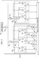
- a shared local delay response generator 44 is inserted into BIST data path BIST_DP for each group 48 of embedded memories 45, at a point following the last of the pipeline delay stages 42 for that group.
- the output of this shared local delay response generator 44 is directly coupled to local comparators 46 associated with those embedded memories 45 in its group 48, with no additional dedicated delay response generators or other delay in BIST data path BIST_DP between shared local delay response generator 44 and any of its associated local comparators 46.
- FIG 4 illustrates the functional arrangement of an example of shared local delay response generator 44j.
- shared local delay response generator 44j includes m buffer stages B0 through Bm-1 (m ⁇ 1), each clocked by a clock signal such as system clock SYS_CLK.
- expected data word EDR in of a width of n bits, is delayed by a time corresponding to m cycles of system clock SYS_CLK before appearing as expected data word EDR out, for application to its associated local comparators 46.
- shared local delay response generator 44 provides the entirety of the local delay in the expected response data applied to local comparators 46 for the embedded memories 45 in the associated group. Conversely, this architecture has no additional local delay response generator that is dedicated to a particular embedded memory 45 within that group. As a result, shared local delay response generator 44 is shared by those embedded memories 45 in SoC 400 that have essentially the same latency as one another. This allows shared local delay response generator 44 to provide the same delay in the expected data response for each memory 45 in that group 48; accordingly, the expected data response is applied by shared local delay response generator 44 simultaneously to each of the local comparators 46 in that group 48.
- the latency time of these memories 45 includes such factors as the operational timing (e.g., read access time) of those memories 45, and other local delays such as those corresponding to the physical length of the data path to those memories 45.
- the delay in the expected data response inserted by shared local delay response generator 44 ensures that the expected data response is applied to local comparators 46 at the correct time for those local comparators 46 to compare the output of their associated embedded memories 45 with the corresponding expected response, in parallel with one another.
- Each local comparator 46 generates a pass/fail signature from the results of these comparisons in the memory test algorithm, and forwards that pass/fail signature to parallel test data comparator 47, which combines the results from local comparators 46 into data for return to BIST controller 40 for this memory type.
- shared local delay response generator 442 for embedded memories 45 in group 482 can insert a different delay into the expected data response for its local comparators 46 than that inserted by local delay response generator 441 for group 481.
- the inserted delay by these local delay response generators 44 may be the same delay, but the physical distance between the groups 481, 482 may be such that a single shared local delay response generator 44 would not work.
- the sharing of a single local delay response generator 44 among multiple embedded memories 45 significantly reduces the chip area required to implement parallel memory test in this BIST context.
- the area required to implement dedicated local delay response generators for each embedded memory can be significant, especially for wide data words.
- this chip area is reduced by the number of embedded memories 45 that can share an instance of shared local delay response generator 44. This area savings is especially significant in those devices in which the memory data path is extremely wide, such as on the order of 128 bits or more.
- one modern SoC device includes as many as twelve instances of 128 bit wide memory that can share a single local delay response generator, resulting in an area reduction of nearly 60% for the memory data path in that device as compared with the conventional BIST architecture with dedicated delay response generators for each memory, such as discussed above relative to FIG 1 .
Landscapes
- Engineering & Computer Science (AREA)
- Computer Hardware Design (AREA)
- General Engineering & Computer Science (AREA)
- Theoretical Computer Science (AREA)
- Computing Systems (AREA)
- Microelectronics & Electronic Packaging (AREA)
- Physics & Mathematics (AREA)
- General Physics & Mathematics (AREA)
- Tests Of Electronic Circuits (AREA)
- For Increasing The Reliability Of Semiconductor Memories (AREA)
- Semiconductor Integrated Circuits (AREA)
Claims (15)
- Integrierte Schaltung, umfassend eine Mehrzahl von Speichern und einen Schaltkreis, der ausgelegt ist, einen Paralleltest der Mehrzahl von Speichern durchzuführen, wobei der Schaltkreis umfasst:eine erste Steuerung (40) zum Generieren eines auf eine oder mehrere Gruppen der Mehrzahl von Speichern (45) anzuwendenden Testdatenmusters;eine erste Gruppe von lokalen Komparatoren (46), wobei jeder lokale Komparator der ersten Gruppe von lokalen Komparatoren (46) mit einem jeweiligen einer ersten Gruppe der Mehrzahl von Speichern (45) assoziiert ist, wobei die erste Gruppe der Mehrzahl von Speichern (45) mindestens zwei Speicher (45) umfasst; undeinen ersten gemeinsamen lokalen Verzögerungsantwortgenerator (44), der gekoppelt ist, um das Testdatenmuster von der ersten Steuerung (40) zu empfangen, und mit jedem der ersten Gruppe von lokalen Komparatoren (46) gekoppelt ist, um eine dem Testdatenmuster entsprechende erwartete Datenantwort auf die erste Gruppe von lokalen Komparatoren (46) nach einer ersten ausgewählten Verzögerung simultan anzuwenden;eine zweite Gruppe von lokalen Komparatoren (46), wobei jeder lokale Komparator der zweiten Gruppe von lokalen Komparatoren (46) mit einem jeweiligen einer zweiten Gruppe der Mehrzahl von Speichern (45) assoziiert ist; undeinen zweiten gemeinsamen lokalen Verzögerungsantwortgenerator (44), der gekoppelt ist, um das Testdatenmuster von der ersten Steuerung zu empfangen, und mit jedem der zweiten Gruppe von lokalen Komparatoren (46) gekoppelt ist, um eine dem Testdatenmuster entsprechende erwartete Datenantwort auf die zweite Gruppe von lokalen Komparatoren (46) nach einer zweiten ausgewählten Verzögerung simultan anzuwenden.
- Integrierte Schaltung nach Anspruch 1, ferner umfassend:
eine oder mehrere Pipelineverzögerungsstufen, die mit einem Ausgang der ersten Steuerung (40) gekoppelt sind, um das Testdatenmuster von der ersten Steuerung (40) zu der ersten Gruppe von Speichern (45) und zu dem ersten gemeinsamen lokalen Verzögerungsantwortgenerator (44) nach einer oder mehreren Verzögerungsperioden weiterzuleiten. - Integrierte Schaltung nach Anspruch 2, umfassend: die zweite Gruppe von lokalen Komparatoren (46), wobei jeder lokale Komparator (46) der zweiten Gruppe von lokalen Komparatoren (46) mit einem jeweiligen einer zweiten Gruppe der Mehrzahl von Speichern (45) assoziiert ist; und den zweiten gemeinsamen lokalen Verzögerungsantwortgenerator (44), der gekoppelt ist, um das Testdatenmuster von einer oder mehreren der Pipelineverzögerungsstufen zu empfangen, und mit jedem der zweiten Gruppe von lokalen Komparatoren (46) gekoppelt ist, um eine dem Testdatenmuster entsprechende erwartete Datenantwort zu der zweiten Gruppe von lokalen Komparatoren (46) nach einer zweiten ausgewählten Verzögerung simultan weiterzuleiten;
wobei mindestens eine der Pipelineverzögerungsstufen dazu dient, das Testdatenmuster von der ersten Steuerung (40) zu der zweiten Gruppe von Speichern (45) und zu dem zweiten gemeinsamen lokalen Verzögerungsantwortgenerator (44) nach einer oder mehreren Verzögerungsperioden weiterzuleiten. - Integrierte Schaltung nach Anspruch 3, ferner umfassend:
mindestens eine zusätzliche Pipelineverzögerungsstufe, die zwischen der ersten Steuerung (40) und der zweiten Gruppe von Speichern (45) gekoppelt ist, und den zweiten gemeinsamen lokalen Verzögerungsantwortgenerator (44). - Integrierte Schaltung nach Anspruch 3, wobei: die erste Steuerung (40) das Testdatenmuster für Speicher (45) eines ersten Speichertyps generiert; und jeder der Speicher (45) der ersten und zweiten Gruppen von Speichern (45) von dem ersten Speichertyp ist.
- Integrierte Schaltung nach Anspruch 1, wobei der erste gemeinsame lokale Verzögerungsantwortgenerator (44) eine oder mehrere in Reihe gekoppelte Verzögerungsstufen umfasst.
- Integrierte Schaltung nach Anspruch 6, wobei jede der Verzögerungsstufen einen getakteten Puffer umfasst.
- Integrierte Schaltung nach Anspruch 1, wobei: das durch die erste Steuerung (40) generierte Testdatenmuster eine ausgewählte Datenwortbreite aufweist; und die ausgewählte Datenwortbreite der breitesten Datenwortbreite der Speicher (45) in der ersten Gruppe der Mehrzahl von Speichern (45) entspricht.
- Integrierte Schaltung nach Anspruch 1, ferner umfassend:eine zweite Steuerung zum Generieren eines auf eine oder mehrere Gruppen der Mehrzahl von Speichern (45) anzuwendenden Testdatenmusters;eine zweite Gruppe von lokalen Komparatoren (46), wobei jeder lokale Komparator der zweiten Gruppe von lokalen Komparatoren (46) mit einem jeweiligen einer zweiten Gruppe der Mehrzahl von Speichern (45) assoziiert ist; undeinen zweiten gemeinsamen lokalen Verzögerungsantwortgenerator (44), der gekoppelt ist, um das Testdatenmuster von der zweiten Steuerung zu empfangen, und mit jedem der zweiten Gruppe von lokalen Komparatoren (46) gekoppelt ist, um eine dem Testdatenmuster entsprechende erwartete Datenantwort auf die erste Gruppe von lokalen Komparatoren (46) nach einer zweiten ausgewählten Verzögerung simultan anzuwenden.
- Integrierte Schaltung nach Anspruch 9, wobei: die erste Steuerung (40) das Testdatenmuster für Speicher (45) eines ersten Speichertyps generiert; jeder der Speicher (45) der ersten Gruppe von Speichern (45) von dem ersten Speichertyp ist; die zweite Steuerung das Testdatenmuster für Speicher (45) eines zweiten Speichertyps generiert; und die zweite Gruppe von Speichern (45) von dem zweiten Speichertyp ist.
- Integrierte Schaltung nach Anspruch 10, wobei der erste Speichertyp einem Einzelport-Speicher entspricht und der zweite Speichertyp einem Doppelport-Speicher entspricht.
- Integrierte Schaltung nach Anspruch 10, wobei der erste Speichertyp einem Direktzugriffsspeicher entspricht und der zweite Speichertyp einem nichtflüchtigen Speicher entspricht.
- Integrierte Schaltung nach Anspruch 1, wobei die integrierte Schaltung ferner mindestens einen Prozessor umfasst, der mit mindestens einem der Speicher (45) gekoppelt ist.
- Integrierte Schaltung nach Anspruch 13, wobei: die integrierte Schaltung von dem Typ Ein-Chip-System (SoC, System-on-a-Chip) ist; und die Mehrzahl von Speichern (45) in die integrierte SoC-Schaltung eingebettete Speicher sind.
- Integrierte Schaltung nach Anspruch 1, wobei die erste ausgewählte Verzögerung einer Speicherzugriffslatenz der Speicher in der ersten Gruppe entspricht.
Applications Claiming Priority (3)
| Application Number | Priority Date | Filing Date | Title |
|---|---|---|---|
| IN5871CH2015 | 2015-10-30 | ||
| US15/066,924 US20170125125A1 (en) | 2015-10-30 | 2016-03-10 | Area-efficient parallel test data path for embedded memories |
| PCT/US2016/059796 WO2017075622A1 (en) | 2015-10-30 | 2016-10-31 | Area-efficient parallel test data path for embedded memories |
Publications (3)
| Publication Number | Publication Date |
|---|---|
| EP3369095A1 EP3369095A1 (de) | 2018-09-05 |
| EP3369095A4 EP3369095A4 (de) | 2019-07-03 |
| EP3369095B1 true EP3369095B1 (de) | 2021-10-27 |
Family
ID=58635757
Family Applications (1)
| Application Number | Title | Priority Date | Filing Date |
|---|---|---|---|
| EP16861067.3A Active EP3369095B1 (de) | 2015-10-30 | 2016-10-31 | Flächeneffizienter paralleltestdatenpfad für eingebettete speicher |
Country Status (3)
| Country | Link |
|---|---|
| US (3) | US20170125125A1 (de) |
| EP (1) | EP3369095B1 (de) |
| CN (2) | CN114639433A (de) |
Families Citing this family (11)
| Publication number | Priority date | Publication date | Assignee | Title |
|---|---|---|---|---|
| US10600495B2 (en) | 2017-06-23 | 2020-03-24 | Texas Instruments Incorporated | Parallel memory self-testing |
| CN108874666A (zh) * | 2018-05-30 | 2018-11-23 | 平安普惠企业管理有限公司 | 测试数据自动生成方法、装置、计算机设备及存储介质 |
| KR20200016680A (ko) * | 2018-08-07 | 2020-02-17 | 삼성전자주식회사 | 피크 노이즈를 감소한 테스트 장치, 테스트 방법 및 테스트가 수행되는 반도체 장치 |
| US11315654B2 (en) * | 2018-10-03 | 2022-04-26 | Arm Limited | Memory testing techniques |
| CN114064557B (zh) * | 2020-07-29 | 2024-08-27 | 瑞昱半导体股份有限公司 | 图形处理装置 |
| CN112540902B (zh) * | 2020-12-03 | 2023-03-14 | 山东云海国创云计算装备产业创新中心有限公司 | 一种片上系统性能检验方法、装置、设备及可读存储介质 |
| US12230345B2 (en) * | 2021-12-08 | 2025-02-18 | Samsung Electronics Co., Ltd. | Built-in self-test circuits for memory systems having multiple channels |
| WO2023141013A1 (en) * | 2022-01-18 | 2023-07-27 | Texas Instruments Incorporated | Methods and apparatus to characterize memory |
| US12147697B2 (en) * | 2022-01-18 | 2024-11-19 | Texas Instruments Incorporated | Methods and apparatus to characterize memory |
| US12283332B2 (en) | 2022-11-22 | 2025-04-22 | Texas Instruments Incorporated | Memory BIST circuit and method |
| CN120950319B (zh) * | 2025-10-17 | 2025-12-23 | 成都融见软件科技有限公司 | 一种基于局部共享期望数据比较器的芯片测试系统 |
Family Cites Families (35)
| Publication number | Priority date | Publication date | Assignee | Title |
|---|---|---|---|---|
| DE2521245C3 (de) * | 1975-05-13 | 1984-03-29 | Siemens AG, 1000 Berlin und 8000 München | Schaltungsanordnung für ein zweikanaliges Sicherheitsschaltwerk mit antivalenter Signalverarbeitung |
| JP2000339996A (ja) * | 1999-05-31 | 2000-12-08 | Nec Corp | 半導体記憶装置およびそのバーンインテスト方法 |
| US6292415B1 (en) * | 1999-09-28 | 2001-09-18 | Aehr Test Systems, Inc. | Enhancements in testing devices on burn-in boards |
| US6553527B1 (en) * | 1999-11-08 | 2003-04-22 | International Business Machines Corporation | Programmable array built-in self test method and controller with programmable expect generator |
| US6934205B1 (en) | 2000-09-06 | 2005-08-23 | Infineon Technologies Aktiengesellschaft | Bist for parallel testing of on chip memory |
| GB0026849D0 (en) * | 2000-11-03 | 2000-12-20 | Acuid Corp Ltd | DDR SDRAM memory test system with fault strobe synchronization |
| US6988232B2 (en) * | 2001-07-05 | 2006-01-17 | Intellitech Corporation | Method and apparatus for optimized parallel testing and access of electronic circuits |
| JP3970716B2 (ja) * | 2002-08-05 | 2007-09-05 | 松下電器産業株式会社 | 半導体記憶装置およびその検査方法 |
| US7305597B1 (en) * | 2003-08-22 | 2007-12-04 | Lsi Corporation | System and method for efficiently testing a large random access memory space |
| US7325178B2 (en) | 2003-12-05 | 2008-01-29 | Texas Instruments Incorporated | Programmable built in self test of memory |
| US7225379B2 (en) * | 2004-04-23 | 2007-05-29 | Oki Electric Industry Co., Ltd. | Circuit and method for testing semiconductor device |
| US7203873B1 (en) * | 2004-06-04 | 2007-04-10 | Magma Design Automation, Inc. | Asynchronous control of memory self test |
| US7324392B2 (en) | 2005-06-09 | 2008-01-29 | Texas Instruments Incorporated | ROM-based memory testing |
| EP1791133A1 (de) * | 2005-11-29 | 2007-05-30 | STMicroelectronics Pvt. Ltd. | Ein Verfahren zur gemeinsamen Nutzung von Testvorrichtungen für mehrere eingebettete Speicher und zugehöriges Speichersystem |
| KR100715679B1 (ko) | 2005-12-05 | 2007-05-09 | 한국전자통신연구원 | 인증 암호화를 통해 보안 전송을 가능하게 하는 gpon시스템 및 그 인증 암호화 방법 |
| JP2007294015A (ja) * | 2006-04-25 | 2007-11-08 | Matsushita Electric Ind Co Ltd | 半導体集積回路、及びbist回路設計方法 |
| US7814385B2 (en) * | 2006-08-30 | 2010-10-12 | Stmicroelectronics Pvt. Ltd. | Self programmable shared bist for testing multiple memories |
| KR100819104B1 (ko) * | 2006-09-07 | 2008-04-03 | 삼성전자주식회사 | 병렬 비트 테스트 회로 및 그에 의한 병렬 비트 테스트방법 |
| US7607060B2 (en) * | 2006-09-12 | 2009-10-20 | International Business Machines Corporation | System and method for performing high speed memory diagnostics via built-in-self-test |
| EP2088442B1 (de) * | 2006-11-10 | 2013-01-09 | NEC Corporation | Parallel-prüfschaltung und verfahren und halbleiteranordnung |
| US7508724B2 (en) | 2006-11-30 | 2009-03-24 | Mosaid Technologies Incorporated | Circuit and method for testing multi-device systems |
| US8384410B1 (en) * | 2007-08-24 | 2013-02-26 | Advantest (Singapore) Pte Ltd | Parallel test circuit with active devices |
| US7805644B2 (en) | 2007-12-29 | 2010-09-28 | Texas Instruments Incorporated | Multiple pBIST controllers |
| KR20090108182A (ko) * | 2008-04-11 | 2009-10-15 | 삼성전자주식회사 | 반도체 메모리 장치의 병렬비트 테스트 회로 |
| JP5167975B2 (ja) | 2008-06-17 | 2013-03-21 | 富士通株式会社 | 半導体装置 |
| JPWO2011001463A1 (ja) * | 2009-06-29 | 2012-12-10 | 株式会社アドバンテスト | 試験装置、校正方法およびプログラム |
| CN101937720A (zh) * | 2010-05-07 | 2011-01-05 | 深圳市忆嘉电子科技有限公司 | 一种高速动态随机存储器测试系统 |
| US8793549B2 (en) * | 2010-08-11 | 2014-07-29 | Lsi Corporation | Low-cost design for register file testability |
| KR20120069404A (ko) * | 2010-12-20 | 2012-06-28 | 삼성전자주식회사 | 테스터 및 이를 포함하는 테스트 시스템 |
| US8843769B2 (en) | 2011-04-18 | 2014-09-23 | Texas Instruments Incorporated | Microcontroller with embedded secure feature |
| GB2498980A (en) * | 2012-02-01 | 2013-08-07 | Inside Secure | Device and method to perform a parallel memory test |
| US8977915B2 (en) | 2012-12-10 | 2015-03-10 | Texas Instruments Incorporated | pBIST engine with reduced SRAM testing bus width |
| US9009550B2 (en) * | 2012-12-10 | 2015-04-14 | Texas Instruments Incorporated | pBIST engine with distributed data logging |
| CN103310850B (zh) * | 2013-06-27 | 2016-01-20 | 桂林电子科技大学 | 片上网络资源节点存储器的内建自测试结构和自测试方法 |
| JP6107612B2 (ja) | 2013-11-14 | 2017-04-05 | 富士通株式会社 | 半導体集積回路、及び、半導体集積回路の試験方法 |
-
2016
- 2016-03-10 US US15/066,924 patent/US20170125125A1/en not_active Abandoned
- 2016-10-31 CN CN202210312951.7A patent/CN114639433A/zh active Pending
- 2016-10-31 CN CN201680061176.5A patent/CN108140418B/zh active Active
- 2016-10-31 EP EP16861067.3A patent/EP3369095B1/de active Active
-
2017
- 2017-02-16 US US15/434,717 patent/US9899103B2/en active Active
-
2018
- 2018-02-14 US US15/896,817 patent/US10460821B2/en active Active
Also Published As
| Publication number | Publication date |
|---|---|
| US20180174663A1 (en) | 2018-06-21 |
| EP3369095A1 (de) | 2018-09-05 |
| US20170157524A1 (en) | 2017-06-08 |
| CN114639433A (zh) | 2022-06-17 |
| EP3369095A4 (de) | 2019-07-03 |
| CN108140418B (zh) | 2022-03-25 |
| US9899103B2 (en) | 2018-02-20 |
| CN108140418A (zh) | 2018-06-08 |
| US20170125125A1 (en) | 2017-05-04 |
| US10460821B2 (en) | 2019-10-29 |
Similar Documents
| Publication | Publication Date | Title |
|---|---|---|
| EP3369095B1 (de) | Flächeneffizienter paralleltestdatenpfad für eingebettete speicher | |
| KR102288558B1 (ko) | 데이터 처리장치의 메모리 내장 자체 테스트 | |
| US10134483B2 (en) | Centralized built-in soft-repair architecture for integrated circuits with embedded memories | |
| CN113167831A (zh) | 在已部署的汽车平台上执行自测的测试系统 | |
| US5574692A (en) | Memory testing apparatus for microelectronic integrated circuit | |
| US8977915B2 (en) | pBIST engine with reduced SRAM testing bus width | |
| CN111033630A (zh) | 具有mbist的多处理器内核设备 | |
| US7805644B2 (en) | Multiple pBIST controllers | |
| JP2013253840A (ja) | 半導体集積回路及びその設計方法 | |
| JP2012104174A (ja) | 試験装置 | |
| CN105518475A (zh) | 柔性接口 | |
| EP4198736A1 (de) | Verteilter mechanismus zur feinkörnigen testleistungssteuerung | |
| US7343480B2 (en) | Single cycle context switching by swapping a primary latch value and a selected secondary latch value in a register file | |
| WO2017075622A1 (en) | Area-efficient parallel test data path for embedded memories | |
| Patil et al. | Implementation of BIST technology for fault detection and repair of the multiported memory using FPGA | |
| TWI410977B (zh) | 測試模組、測試裝置與測試方法 | |
| US7844871B2 (en) | Test interface for memory elements | |
| US10043027B1 (en) | Generation of mask-value pairs for managing access to memory segments | |
| CN103871476B (zh) | 嵌入式存储器测试系统 | |
| US20100115353A1 (en) | System and method for testing application-specific blocks embedded in reconfigurable arrays | |
| JP7394849B2 (ja) | メモリ組込み自己テストコントローラを用いる読み出し専用メモリのテスト | |
| Jone et al. | An efficient BIST method for distributed small buffers | |
| US8966124B1 (en) | Systems, methods, and articles of manufacture to stream data | |
| US8819509B2 (en) | Integrated circuit, test circuit, and method of testing | |
| US20240338289A1 (en) | Method of performance harvesting in core matrix structure and device of performing the same |
Legal Events
| Date | Code | Title | Description |
|---|---|---|---|
| STAA | Information on the status of an ep patent application or granted ep patent |
Free format text: STATUS: THE INTERNATIONAL PUBLICATION HAS BEEN MADE |
|
| PUAI | Public reference made under article 153(3) epc to a published international application that has entered the european phase |
Free format text: ORIGINAL CODE: 0009012 |
|
| STAA | Information on the status of an ep patent application or granted ep patent |
Free format text: STATUS: REQUEST FOR EXAMINATION WAS MADE |
|
| 17P | Request for examination filed |
Effective date: 20180530 |
|
| AK | Designated contracting states |
Kind code of ref document: A1 Designated state(s): AL AT BE BG CH CY CZ DE DK EE ES FI FR GB GR HR HU IE IS IT LI LT LU LV MC MK MT NL NO PL PT RO RS SE SI SK SM TR |
|
| AX | Request for extension of the european patent |
Extension state: BA ME |
|
| DAV | Request for validation of the european patent (deleted) | ||
| DAX | Request for extension of the european patent (deleted) | ||
| RIC1 | Information provided on ipc code assigned before grant |
Ipc: G11C 29/38 20060101AFI20190123BHEP Ipc: G11C 29/26 20060101ALI20190123BHEP Ipc: G06F 11/27 20060101ALI20190123BHEP |
|
| REG | Reference to a national code |
Ref country code: DE Ref legal event code: R079 Ref document number: 602016065564 Country of ref document: DE Free format text: PREVIOUS MAIN CLASS: G11C0029120000 Ipc: G11C0029380000 |
|
| A4 | Supplementary search report drawn up and despatched |
Effective date: 20190531 |
|
| RIC1 | Information provided on ipc code assigned before grant |
Ipc: G11C 29/26 20060101ALI20190524BHEP Ipc: G06F 11/27 20060101ALI20190524BHEP Ipc: G11C 29/38 20060101AFI20190524BHEP |
|
| STAA | Information on the status of an ep patent application or granted ep patent |
Free format text: STATUS: EXAMINATION IS IN PROGRESS |
|
| 17Q | First examination report despatched |
Effective date: 20200414 |
|
| GRAP | Despatch of communication of intention to grant a patent |
Free format text: ORIGINAL CODE: EPIDOSNIGR1 |
|
| STAA | Information on the status of an ep patent application or granted ep patent |
Free format text: STATUS: GRANT OF PATENT IS INTENDED |
|
| INTG | Intention to grant announced |
Effective date: 20210616 |
|
| GRAS | Grant fee paid |
Free format text: ORIGINAL CODE: EPIDOSNIGR3 |
|
| GRAA | (expected) grant |
Free format text: ORIGINAL CODE: 0009210 |
|
| STAA | Information on the status of an ep patent application or granted ep patent |
Free format text: STATUS: THE PATENT HAS BEEN GRANTED |
|
| AK | Designated contracting states |
Kind code of ref document: B1 Designated state(s): AL AT BE BG CH CY CZ DE DK EE ES FI FR GB GR HR HU IE IS IT LI LT LU LV MC MK MT NL NO PL PT RO RS SE SI SK SM TR |
|
| REG | Reference to a national code |
Ref country code: GB Ref legal event code: FG4D |
|
| REG | Reference to a national code |
Ref country code: CH Ref legal event code: EP |
|
| REG | Reference to a national code |
Ref country code: AT Ref legal event code: REF Ref document number: 1442553 Country of ref document: AT Kind code of ref document: T Effective date: 20211115 |
|
| REG | Reference to a national code |
Ref country code: DE Ref legal event code: R096 Ref document number: 602016065564 Country of ref document: DE |
|
| REG | Reference to a national code |
Ref country code: IE Ref legal event code: FG4D |
|
| REG | Reference to a national code |
Ref country code: LT Ref legal event code: MG9D |
|
| REG | Reference to a national code |
Ref country code: NL Ref legal event code: MP Effective date: 20211027 |
|
| REG | Reference to a national code |
Ref country code: AT Ref legal event code: MK05 Ref document number: 1442553 Country of ref document: AT Kind code of ref document: T Effective date: 20211027 |
|
| PG25 | Lapsed in a contracting state [announced via postgrant information from national office to epo] |
Ref country code: RS Free format text: LAPSE BECAUSE OF FAILURE TO SUBMIT A TRANSLATION OF THE DESCRIPTION OR TO PAY THE FEE WITHIN THE PRESCRIBED TIME-LIMIT Effective date: 20211027 Ref country code: LT Free format text: LAPSE BECAUSE OF FAILURE TO SUBMIT A TRANSLATION OF THE DESCRIPTION OR TO PAY THE FEE WITHIN THE PRESCRIBED TIME-LIMIT Effective date: 20211027 Ref country code: FI Free format text: LAPSE BECAUSE OF FAILURE TO SUBMIT A TRANSLATION OF THE DESCRIPTION OR TO PAY THE FEE WITHIN THE PRESCRIBED TIME-LIMIT Effective date: 20211027 Ref country code: BG Free format text: LAPSE BECAUSE OF FAILURE TO SUBMIT A TRANSLATION OF THE DESCRIPTION OR TO PAY THE FEE WITHIN THE PRESCRIBED TIME-LIMIT Effective date: 20220127 Ref country code: AT Free format text: LAPSE BECAUSE OF FAILURE TO SUBMIT A TRANSLATION OF THE DESCRIPTION OR TO PAY THE FEE WITHIN THE PRESCRIBED TIME-LIMIT Effective date: 20211027 |
|
| REG | Reference to a national code |
Ref country code: CH Ref legal event code: PL |
|
| PG25 | Lapsed in a contracting state [announced via postgrant information from national office to epo] |
Ref country code: IS Free format text: LAPSE BECAUSE OF FAILURE TO SUBMIT A TRANSLATION OF THE DESCRIPTION OR TO PAY THE FEE WITHIN THE PRESCRIBED TIME-LIMIT Effective date: 20220227 Ref country code: SE Free format text: LAPSE BECAUSE OF FAILURE TO SUBMIT A TRANSLATION OF THE DESCRIPTION OR TO PAY THE FEE WITHIN THE PRESCRIBED TIME-LIMIT Effective date: 20211027 Ref country code: PT Free format text: LAPSE BECAUSE OF FAILURE TO SUBMIT A TRANSLATION OF THE DESCRIPTION OR TO PAY THE FEE WITHIN THE PRESCRIBED TIME-LIMIT Effective date: 20220228 Ref country code: PL Free format text: LAPSE BECAUSE OF FAILURE TO SUBMIT A TRANSLATION OF THE DESCRIPTION OR TO PAY THE FEE WITHIN THE PRESCRIBED TIME-LIMIT Effective date: 20211027 Ref country code: NO Free format text: LAPSE BECAUSE OF FAILURE TO SUBMIT A TRANSLATION OF THE DESCRIPTION OR TO PAY THE FEE WITHIN THE PRESCRIBED TIME-LIMIT Effective date: 20220127 Ref country code: NL Free format text: LAPSE BECAUSE OF FAILURE TO SUBMIT A TRANSLATION OF THE DESCRIPTION OR TO PAY THE FEE WITHIN THE PRESCRIBED TIME-LIMIT Effective date: 20211027 Ref country code: LV Free format text: LAPSE BECAUSE OF FAILURE TO SUBMIT A TRANSLATION OF THE DESCRIPTION OR TO PAY THE FEE WITHIN THE PRESCRIBED TIME-LIMIT Effective date: 20211027 Ref country code: HR Free format text: LAPSE BECAUSE OF FAILURE TO SUBMIT A TRANSLATION OF THE DESCRIPTION OR TO PAY THE FEE WITHIN THE PRESCRIBED TIME-LIMIT Effective date: 20211027 Ref country code: GR Free format text: LAPSE BECAUSE OF FAILURE TO SUBMIT A TRANSLATION OF THE DESCRIPTION OR TO PAY THE FEE WITHIN THE PRESCRIBED TIME-LIMIT Effective date: 20220128 Ref country code: ES Free format text: LAPSE BECAUSE OF FAILURE TO SUBMIT A TRANSLATION OF THE DESCRIPTION OR TO PAY THE FEE WITHIN THE PRESCRIBED TIME-LIMIT Effective date: 20211027 |
|
| REG | Reference to a national code |
Ref country code: BE Ref legal event code: MM Effective date: 20211031 |
|
| REG | Reference to a national code |
Ref country code: DE Ref legal event code: R097 Ref document number: 602016065564 Country of ref document: DE |
|
| PG25 | Lapsed in a contracting state [announced via postgrant information from national office to epo] |
Ref country code: SM Free format text: LAPSE BECAUSE OF FAILURE TO SUBMIT A TRANSLATION OF THE DESCRIPTION OR TO PAY THE FEE WITHIN THE PRESCRIBED TIME-LIMIT Effective date: 20211027 Ref country code: SK Free format text: LAPSE BECAUSE OF FAILURE TO SUBMIT A TRANSLATION OF THE DESCRIPTION OR TO PAY THE FEE WITHIN THE PRESCRIBED TIME-LIMIT Effective date: 20211027 Ref country code: RO Free format text: LAPSE BECAUSE OF FAILURE TO SUBMIT A TRANSLATION OF THE DESCRIPTION OR TO PAY THE FEE WITHIN THE PRESCRIBED TIME-LIMIT Effective date: 20211027 Ref country code: MC Free format text: LAPSE BECAUSE OF FAILURE TO SUBMIT A TRANSLATION OF THE DESCRIPTION OR TO PAY THE FEE WITHIN THE PRESCRIBED TIME-LIMIT Effective date: 20211027 Ref country code: LU Free format text: LAPSE BECAUSE OF NON-PAYMENT OF DUE FEES Effective date: 20211031 Ref country code: EE Free format text: LAPSE BECAUSE OF FAILURE TO SUBMIT A TRANSLATION OF THE DESCRIPTION OR TO PAY THE FEE WITHIN THE PRESCRIBED TIME-LIMIT Effective date: 20211027 Ref country code: DK Free format text: LAPSE BECAUSE OF FAILURE TO SUBMIT A TRANSLATION OF THE DESCRIPTION OR TO PAY THE FEE WITHIN THE PRESCRIBED TIME-LIMIT Effective date: 20211027 Ref country code: CZ Free format text: LAPSE BECAUSE OF FAILURE TO SUBMIT A TRANSLATION OF THE DESCRIPTION OR TO PAY THE FEE WITHIN THE PRESCRIBED TIME-LIMIT Effective date: 20211027 Ref country code: BE Free format text: LAPSE BECAUSE OF NON-PAYMENT OF DUE FEES Effective date: 20211031 |
|
| PG25 | Lapsed in a contracting state [announced via postgrant information from national office to epo] |
Ref country code: LI Free format text: LAPSE BECAUSE OF NON-PAYMENT OF DUE FEES Effective date: 20211031 Ref country code: CH Free format text: LAPSE BECAUSE OF NON-PAYMENT OF DUE FEES Effective date: 20211031 |
|
| PLBE | No opposition filed within time limit |
Free format text: ORIGINAL CODE: 0009261 |
|
| STAA | Information on the status of an ep patent application or granted ep patent |
Free format text: STATUS: NO OPPOSITION FILED WITHIN TIME LIMIT |
|
| 26N | No opposition filed |
Effective date: 20220728 |
|
| PG25 | Lapsed in a contracting state [announced via postgrant information from national office to epo] |
Ref country code: IE Free format text: LAPSE BECAUSE OF NON-PAYMENT OF DUE FEES Effective date: 20211031 Ref country code: AL Free format text: LAPSE BECAUSE OF FAILURE TO SUBMIT A TRANSLATION OF THE DESCRIPTION OR TO PAY THE FEE WITHIN THE PRESCRIBED TIME-LIMIT Effective date: 20211027 |
|
| PG25 | Lapsed in a contracting state [announced via postgrant information from national office to epo] |
Ref country code: SI Free format text: LAPSE BECAUSE OF FAILURE TO SUBMIT A TRANSLATION OF THE DESCRIPTION OR TO PAY THE FEE WITHIN THE PRESCRIBED TIME-LIMIT Effective date: 20211027 |
|
| PG25 | Lapsed in a contracting state [announced via postgrant information from national office to epo] |
Ref country code: IT Free format text: LAPSE BECAUSE OF FAILURE TO SUBMIT A TRANSLATION OF THE DESCRIPTION OR TO PAY THE FEE WITHIN THE PRESCRIBED TIME-LIMIT Effective date: 20211027 Ref country code: HU Free format text: LAPSE BECAUSE OF FAILURE TO SUBMIT A TRANSLATION OF THE DESCRIPTION OR TO PAY THE FEE WITHIN THE PRESCRIBED TIME-LIMIT; INVALID AB INITIO Effective date: 20161031 |
|
| P01 | Opt-out of the competence of the unified patent court (upc) registered |
Effective date: 20230523 |
|
| PG25 | Lapsed in a contracting state [announced via postgrant information from national office to epo] |
Ref country code: CY Free format text: LAPSE BECAUSE OF FAILURE TO SUBMIT A TRANSLATION OF THE DESCRIPTION OR TO PAY THE FEE WITHIN THE PRESCRIBED TIME-LIMIT Effective date: 20211027 |
|
| PG25 | Lapsed in a contracting state [announced via postgrant information from national office to epo] |
Ref country code: MK Free format text: LAPSE BECAUSE OF FAILURE TO SUBMIT A TRANSLATION OF THE DESCRIPTION OR TO PAY THE FEE WITHIN THE PRESCRIBED TIME-LIMIT Effective date: 20211027 |
|
| PG25 | Lapsed in a contracting state [announced via postgrant information from national office to epo] |
Ref country code: TR Free format text: LAPSE BECAUSE OF FAILURE TO SUBMIT A TRANSLATION OF THE DESCRIPTION OR TO PAY THE FEE WITHIN THE PRESCRIBED TIME-LIMIT Effective date: 20211027 |
|
| PG25 | Lapsed in a contracting state [announced via postgrant information from national office to epo] |
Ref country code: MT Free format text: LAPSE BECAUSE OF FAILURE TO SUBMIT A TRANSLATION OF THE DESCRIPTION OR TO PAY THE FEE WITHIN THE PRESCRIBED TIME-LIMIT Effective date: 20211027 |
|
| PGFP | Annual fee paid to national office [announced via postgrant information from national office to epo] |
Ref country code: GB Payment date: 20250923 Year of fee payment: 10 |
|
| PGFP | Annual fee paid to national office [announced via postgrant information from national office to epo] |
Ref country code: FR Payment date: 20250924 Year of fee payment: 10 |
|
| PGFP | Annual fee paid to national office [announced via postgrant information from national office to epo] |
Ref country code: DE Payment date: 20250923 Year of fee payment: 10 |