EP3370330B1 - Schaltnetzteil mit zwei leistungsumrichtern und korrekturmöglichkeit der statik - Google Patents
Schaltnetzteil mit zwei leistungsumrichtern und korrekturmöglichkeit der statik Download PDFInfo
- Publication number
- EP3370330B1 EP3370330B1 EP16870343.7A EP16870343A EP3370330B1 EP 3370330 B1 EP3370330 B1 EP 3370330B1 EP 16870343 A EP16870343 A EP 16870343A EP 3370330 B1 EP3370330 B1 EP 3370330B1
- Authority
- EP
- European Patent Office
- Prior art keywords
- power converter
- droop characteristic
- output voltage
- correction value
- correction
- Prior art date
- Legal status (The legal status is an assumption and is not a legal conclusion. Google has not performed a legal analysis and makes no representation as to the accuracy of the status listed.)
- Active
Links
Images
Classifications
-
- H—ELECTRICITY
- H02—GENERATION; CONVERSION OR DISTRIBUTION OF ELECTRIC POWER
- H02M—APPARATUS FOR CONVERSION BETWEEN AC AND AC, BETWEEN AC AND DC, OR BETWEEN DC AND DC, AND FOR USE WITH MAINS OR SIMILAR POWER SUPPLY SYSTEMS; CONVERSION OF DC OR AC INPUT POWER INTO SURGE OUTPUT POWER; CONTROL OR REGULATION THEREOF
- H02M3/00—Conversion of DC power input into DC power output
- H02M3/02—Conversion of DC power input into DC power output without intermediate conversion into AC
- H02M3/04—Conversion of DC power input into DC power output without intermediate conversion into AC by static converters
- H02M3/10—Conversion of DC power input into DC power output without intermediate conversion into AC by static converters using discharge tubes with control electrode or semiconductor devices with control electrode
- H02M3/145—Conversion of DC power input into DC power output without intermediate conversion into AC by static converters using discharge tubes with control electrode or semiconductor devices with control electrode using devices of a triode or transistor type requiring continuous application of a control signal
- H02M3/155—Conversion of DC power input into DC power output without intermediate conversion into AC by static converters using discharge tubes with control electrode or semiconductor devices with control electrode using devices of a triode or transistor type requiring continuous application of a control signal using semiconductor devices only
-
- H—ELECTRICITY
- H02—GENERATION; CONVERSION OR DISTRIBUTION OF ELECTRIC POWER
- H02M—APPARATUS FOR CONVERSION BETWEEN AC AND AC, BETWEEN AC AND DC, OR BETWEEN DC AND DC, AND FOR USE WITH MAINS OR SIMILAR POWER SUPPLY SYSTEMS; CONVERSION OF DC OR AC INPUT POWER INTO SURGE OUTPUT POWER; CONTROL OR REGULATION THEREOF
- H02M3/00—Conversion of DC power input into DC power output
- H02M3/02—Conversion of DC power input into DC power output without intermediate conversion into AC
- H02M3/04—Conversion of DC power input into DC power output without intermediate conversion into AC by static converters
- H02M3/10—Conversion of DC power input into DC power output without intermediate conversion into AC by static converters using discharge tubes with control electrode or semiconductor devices with control electrode
- H02M3/145—Conversion of DC power input into DC power output without intermediate conversion into AC by static converters using discharge tubes with control electrode or semiconductor devices with control electrode using devices of a triode or transistor type requiring continuous application of a control signal
- H02M3/155—Conversion of DC power input into DC power output without intermediate conversion into AC by static converters using discharge tubes with control electrode or semiconductor devices with control electrode using devices of a triode or transistor type requiring continuous application of a control signal using semiconductor devices only
- H02M3/156—Conversion of DC power input into DC power output without intermediate conversion into AC by static converters using discharge tubes with control electrode or semiconductor devices with control electrode using devices of a triode or transistor type requiring continuous application of a control signal using semiconductor devices only with automatic control of output voltage or current, e.g. switching regulators
- H02M3/158—Conversion of DC power input into DC power output without intermediate conversion into AC by static converters using discharge tubes with control electrode or semiconductor devices with control electrode using devices of a triode or transistor type requiring continuous application of a control signal using semiconductor devices only with automatic control of output voltage or current, e.g. switching regulators including plural semiconductor devices as final control devices for a single load
- H02M3/1584—Conversion of DC power input into DC power output without intermediate conversion into AC by static converters using discharge tubes with control electrode or semiconductor devices with control electrode using devices of a triode or transistor type requiring continuous application of a control signal using semiconductor devices only with automatic control of output voltage or current, e.g. switching regulators including plural semiconductor devices as final control devices for a single load with a plurality of power processing stages connected in parallel
-
- H—ELECTRICITY
- H02—GENERATION; CONVERSION OR DISTRIBUTION OF ELECTRIC POWER
- H02M—APPARATUS FOR CONVERSION BETWEEN AC AND AC, BETWEEN AC AND DC, OR BETWEEN DC AND DC, AND FOR USE WITH MAINS OR SIMILAR POWER SUPPLY SYSTEMS; CONVERSION OF DC OR AC INPUT POWER INTO SURGE OUTPUT POWER; CONTROL OR REGULATION THEREOF
- H02M3/00—Conversion of DC power input into DC power output
- H02M3/02—Conversion of DC power input into DC power output without intermediate conversion into AC
- H02M3/04—Conversion of DC power input into DC power output without intermediate conversion into AC by static converters
- H02M3/06—Conversion of DC power input into DC power output without intermediate conversion into AC by static converters using resistors or capacitors, e.g. potential divider
- H02M3/07—Conversion of DC power input into DC power output without intermediate conversion into AC by static converters using resistors or capacitors, e.g. potential divider using capacitors charged and discharged alternately by semiconductor devices with control electrode, e.g. charge pumps
-
- H—ELECTRICITY
- H03—ELECTRONIC CIRCUITRY
- H03K—PULSE TECHNIQUE
- H03K17/00—Electronic switching or gating, i.e. not by contact-making and –breaking
- H03K17/14—Modifications for compensating variations of physical values, e.g. of temperature
- H03K17/145—Modifications for compensating variations of physical values, e.g. of temperature in field-effect transistor switches
-
- H—ELECTRICITY
- H03—ELECTRONIC CIRCUITRY
- H03K—PULSE TECHNIQUE
- H03K3/00—Circuits for generating electric pulses; Monostable, bistable or multistable circuits
- H03K3/02—Generators characterised by the type of circuit or by the means used for producing pulses
- H03K3/53—Generators characterised by the type of circuit or by the means used for producing pulses by the use of an energy-accumulating element discharged through the load by a switching device controlled by an external signal and not incorporating positive feedback
- H03K3/57—Generators characterised by the type of circuit or by the means used for producing pulses by the use of an energy-accumulating element discharged through the load by a switching device controlled by an external signal and not incorporating positive feedback the switching device being a semiconductor device
-
- H—ELECTRICITY
- H02—GENERATION; CONVERSION OR DISTRIBUTION OF ELECTRIC POWER
- H02M—APPARATUS FOR CONVERSION BETWEEN AC AND AC, BETWEEN AC AND DC, OR BETWEEN DC AND DC, AND FOR USE WITH MAINS OR SIMILAR POWER SUPPLY SYSTEMS; CONVERSION OF DC OR AC INPUT POWER INTO SURGE OUTPUT POWER; CONTROL OR REGULATION THEREOF
- H02M3/00—Conversion of DC power input into DC power output
- H02M3/02—Conversion of DC power input into DC power output without intermediate conversion into AC
- H02M3/04—Conversion of DC power input into DC power output without intermediate conversion into AC by static converters
- H02M3/10—Conversion of DC power input into DC power output without intermediate conversion into AC by static converters using discharge tubes with control electrode or semiconductor devices with control electrode
- H02M3/145—Conversion of DC power input into DC power output without intermediate conversion into AC by static converters using discharge tubes with control electrode or semiconductor devices with control electrode using devices of a triode or transistor type requiring continuous application of a control signal
- H02M3/155—Conversion of DC power input into DC power output without intermediate conversion into AC by static converters using discharge tubes with control electrode or semiconductor devices with control electrode using devices of a triode or transistor type requiring continuous application of a control signal using semiconductor devices only
- H02M3/156—Conversion of DC power input into DC power output without intermediate conversion into AC by static converters using discharge tubes with control electrode or semiconductor devices with control electrode using devices of a triode or transistor type requiring continuous application of a control signal using semiconductor devices only with automatic control of output voltage or current, e.g. switching regulators
- H02M3/158—Conversion of DC power input into DC power output without intermediate conversion into AC by static converters using discharge tubes with control electrode or semiconductor devices with control electrode using devices of a triode or transistor type requiring continuous application of a control signal using semiconductor devices only with automatic control of output voltage or current, e.g. switching regulators including plural semiconductor devices as final control devices for a single load
Definitions
- the present invention relates to a switching power-supply apparatus including power converters connected in parallel, and a droop characteristic correction method performed by the switching power-supply apparatus.
- a DC power-supply apparatus according to the preamble of claim 1 is known from WO2015/159785 A1 .
- Patent Document 1 further discloses a DC power-supply apparatus for performing parallel operation of a plurality of DC power supplies connected in parallel.
- the DC power-supply apparatus described in Patent Document 1 performs droop control in which as a detected output current of a DC power supply increases, an output voltage is reduced.
- droop characteristics of the respective DC power supplies vary, there is a risk that currents concentrate on one DC power supply, an overcurrent state occurs, and more heat is generated.
- a maximum output power of the whole apparatus falls below an expected value. Accordingly, it is important to control load factors of the respective DC power supplies to be even.
- Patent Document 1 Japanese Unexamined Patent Application Publication No.8-289468
- the droop characteristics may vary due to variations in characteristics of individual components.
- it may be considered, for example, before factory shipment, to calculate a correction value from a detection result of an output voltage with respect to an output current, store the correction value in a memory, and correct a droop characteristic using the stored correction value when actually used.
- Patent Document 1 only a total output current of the plurality of DC power supplies connected in parallel is detectable. Accordingly, the same correction value is to be used for droop characteristics set for each of the plurality of DC power supplies. As a result, it is difficult to correct variations in detection results of output currents of the respective DC power supplies separately and precisely.
- the present invention aims to provide a switching power-supply apparatus and a droop characteristic correction method capable of correcting variations in droop characteristics generated for respective power converters.
- the present invention provides a switching power-supply apparatus according to claim 1 and a corresponding droop characteristic correction method performed by a switching power-supply apparatus according to claim 4.
- Preferred embodiments are defined in the dependent claims.
- a switching power-supply apparatus includes: a first power converter and a second power converter connected in parallel, a first output voltage detector configured to detect a magnitude of an output voltage of the first power converter, a first controller configured to perform PWM control on the first power converter so as to equalize a magnitude of an output voltage detected by the first output voltage detector and a target voltage value, a second output voltage detector configured to detect a magnitude of an output voltage of the second power converter, a second controller configured to perform PWM control on the second power converter so as to equalize a magnitude of an output voltage detected by the second output voltage detector and the target voltage value, a first droop characteristic generator configured to generate a droop characteristic that reduces an output voltage of the first power converter as an output current of the first power converter increases, a second droop characteristic generator configured to generate a droop characteristic that reduces an output voltage of the second power converter as an output current of the second power converter increases, an operation selector configured to make only selected one of the first power converter and the second power
- the detected output current and output voltage of the switching power-supply apparatus correspond to an output current and an output voltage, respectively, of one of the first power converter and the second power converter made to operate.
- a droop characteristic of each of the first power converter and the second power converter may be obtained from this detection result.
- a correction value of the droop characteristic may be obtained for each of the first power converter and the second power converter.
- variations in the droop characteristics may be eliminated by correcting the droop characteristics of the first power converter and the second power converter separately. Accordingly, variations in output currents of the first power converter and the second power converter may be prevented, thereby making it unnecessary to design a switching power-supply apparatus in consideration of the variations, and also enabling the size of a switching power-supply apparatus to be reduced.
- the switching power-supply apparatus may have a configuration that the first receiver receives a first voltage offset value adapted to the first power converter, the second receiver receives a second voltage offset value adapted to the second power converter, the first correction unit corrects a magnitude of an output voltage detected by the first output voltage detector with the first voltage offset value, and the second correction unit corrects a magnitude of an output voltage detected by the second output voltage detector with the second voltage offset value.
- the switching power-supply apparatus may include means for prohibiting modification of a first correction value and a second correction value stored in the storage unit.
- the method includes: a first generation step of generating a droop characteristic that reduces an output voltage of the first power converter as an output current of the first power converter increases; a second generation step of generating a droop characteristic that reduces an output voltage of the second power converter as an output current of the second power converter increases; an action selection step of making only selected one of the first power converter and the second power converter operate; a first receiving step of receiving from an external device a first correction value that corrects a droop characteristic generated in the first generating step; a second receiving step of receiving from the external device a second correction value that corrects a droop characteristic generated in the second generating step; a storage step of storing a first correction value received in the first receiving step and a second correction value received in the second receiving step; a first correction step of correcting a droop characteristic generated in the first generation step with the first correction value; and a second correction step of correcting a droop characteristic generated in the second generation step with the second correction value.
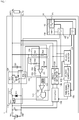
- the correction value for drooping increases as the output current increases.
- These correction values for drooping are inputted into the voltage detectors 15A and 15B, respectively.
- apparent magnitudes of output voltages detected by the respective voltage detectors 15A and 15B increase.
- the PWM signal output unit 13A described later controls the converter 11A
- the PWM signal output unit 13B described later controls the converter 11B so as to decrease the output voltage.
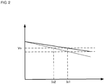
- the converters 11A and 11B have such characteristics that output voltages thereof reduce as output currents increase, respectively.
- the voltage detectors 15A and 15B each include voltage-dividing resistors R21 and R22, and detect the output voltages of the converters 11A and 11B (specifically, divided voltages thereof), respectively.
- a node between the voltage-dividing resistors R21 and R22 in the voltage detector 15A is connected to the voltage controller 14A, and a node between the voltage-dividing resistors R21 and R22 in the voltage detector 15B is connected to the voltage controller 14B.
- the voltage detector 15A corresponds to a "first output voltage detector” according to the present invention.
- the voltage detector 15B corresponds to a "second output voltage detector” according to the present invention.
- the error amplifier 141 in the voltage controller 14A amplifies an error between the output voltage of the converter 11A and the reference voltage Vref and outputs the resultant signal
- the error amplifier 141 in the voltage controller 14B amplifies an error between the output voltage of the converter 11B and the reference voltage Vref and outputs the resultant signal.
- An output signal from the error amplifiers 141 in the voltage controller 14A is inputted into the PWM signal output unit 13A
- an output signal from the error amplifier 141 in the voltage controller 14B is inputted into the PWM signal output unit 13B.
- the clock generator 133 outputs a clock signal to the AND gate 131. Note that, the clock generator 133 of the voltage controller 14A and the clock generator 133 of the voltage controller 14B generate clock signals having different phases from each other.
- An output signal from the voltage controller 14A and a clock signal generated by the clock generator 133 are inputted into the comparator 132 in the PWM signal output unit 13A, and an output signal from the voltage controller 14B and a clock signal generated by the clock generator 133 are inputted into the comparator 132 in the PWM signal output unit 13B.
- the comparator 132 generates a PWM signal from the two signals and outputs the PWM signal.
- the PWM signal outputted from the comparator 132 is inputted through the AND gate 131 to the switch Q11. As described above, the PWM signal output units 13A and 13B perform PWM control on the converters 11A and 11B, respectively.
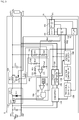
- the correction value for the gain of the variable gain amplifier G11 is determined.
- the switching unit 161 When a correction value (second correction value) for the gain of the variable gain amplifier of the droop characteristic generator 12B is determined, the switching unit 161 outputs the L-level signal to the AND gate 131 of the PWM signal output unit 13A to halt operation of the converter 11A. The switching unit 161 outputs the H-level signal to the AND gate of the PWM signal output unit 13B. Then, same operations as the above-described (2) to (5) are performed.
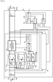
- Fig. 4 is a circuit diagram of a switching power-supply apparatus 3 according to Embodiment 3.
- the microcomputer 16 receives from the measuring jig a correction value adapted to the converter unit 31.
- the correction unit 162 corrects, based on the correction value, a gain of a variable gain amplifier of the droop characteristic generator 12A included in the converter unit 31, to correct a correction value for drooping.
- the microcomputer 16 receives a correction value adapted to the converter unit 32 from the measuring jig.
- the correction unit 162 corrects, based on the correction value, a gain of a variable gain amplifier of a droop characteristic generator included in the converter unit 32, to correct a correction value for drooping.
Landscapes
- Engineering & Computer Science (AREA)
- Power Engineering (AREA)
- Dc-Dc Converters (AREA)
Claims (4)
- Schaltnetzteil, umfassend:einen ersten Leistungsumrichter (11A) und einen zweiten Leistungsumrichter (11B), die parallel geschaltet sind;einen ersten Ausgangsspannungsdetektor (15A), der konfiguriert ist, eine Größe einer Ausgangsspannung des ersten Leistungsumrichters zu detektieren;ein erstes Steuergerät (14A), das konfiguriert ist, PWM-Steuerung an dem ersten Leistungsumrichter vorzunehmen, um eine Größe einer von dem ersten Ausgangsspannungsdetektor detektierten Ausgangsspannung und einen Sollspannungswert anzugleichen;einen zweiten Ausgangsspannungsdetektor (15B), der konfiguriert ist, eine Größe einer Ausgangsspannung des zweiten Leistungsumrichters zu detektieren;ein zweites Steuergerät (14B), das konfiguriert ist, PWM-Steuerung an dem zweiten Leistungsumrichter vorzunehmen, um eine Größe einer von dem zweiten Ausgangsspannungsdetektor detektierten Ausgangsspannung und den Sollspannungswert anzugleichen;einen ersten Statik-Generator (12A), der konfiguriert ist, eine Statik zu erzeugen, die eine Ausgangsspannung des ersten Leistungsumrichters bei Zunahme eines Ausgangsstroms des ersten Leistungsumrichters reduziert;einen zweiten Statik-Generator (12B), der konfiguriert ist, eine Statik zu erzeugen, die eine Ausgangsspannung des zweiten Leistungsumrichters bei Zunahme eines Ausgangsstroms des zweiten Leistungsumrichters reduziert;gekennzeichnet durcheinen Betriebswähler (161), der konfiguriert ist, entweder nur den gewählten erstem Leistungsumrichter oder nur den gewählten zweiten Leistungsumrichter arbeiten zu lassen;einen ersten Empfänger (163), der konfiguriert ist, von einer externen Vorrichtung einen ersten Korrekturwert zum Korrigieren einer von dem ersten Statik-Generator (12A) erzeugten Statik zu empfangen;einen zweiten Empfänger (163), der konfiguriert ist, von der externen Vorrichtung einen zweiten Korrekturwert zum Korrigieren einer von dem zweiten Statik-Generator (12B) erzeugten Statik zu empfangen;eine Speichereinheit (164), die konfiguriert ist, einen von dem ersten Empfänger empfangenen ersten Korrekturwert und einen von dem zweiten Empfänger empfangenen zweiten Korrekturwert zu speichern;eine erste Korrektureinheit (162), die konfiguriert ist, eine von dem ersten Statik-Generator erzeugte Statik mit dem ersten Korrekturwert zu korrigieren; undeine zweite Korrektureinheit (162), die konfiguriert ist, eine von dem zweiten Statik-Generator erzeugte Statik mit dem zweiten Korrekturwert zu korrigieren.
- Schaltnetzteil nach Anspruch 1, wobeider erste Empfänger (163) einen auf den ersten Leistungsumrichter abgestimmten ersten Spannungsoffsetwert empfängt,der zweite Empfänger (163) einen auf den zweiten Leistungsumrichter abgestimmten zweiten Spannungsoffsetwert empfängt,die erste Korrektureinheit (162) eine Größe einer von dem ersten Ausgangsspannungsdetektor detektierten Ausgangsspannung mit dem ersten Spannungsoffsetwert korrigiert unddie zweite Korrektureinheit (162) eine Größe einer von dem zweiten Ausgangsspannungsdetektor detektierten Ausgangsspannung mit dem zweiten Spannungsoffsetwert korrigiert.
- Schaltnetzteil nach Anspruch 1 oder 2, weiterhin umfassend:
Mittel zum Unterbinden von Änderung eines ersten Korrekturwerts und eines zweiten Korrekturwerts, die in der Speichereinheit gespeichert sind. - Statik-Korrekturverfahren, welches von einem Schaltnetzteil ausgeführt wird, das PWM-Steuerung separat an einem ersten Leistungsumrichter (11A) und einem zweiten Leistungsumrichter (11B), die parallel geschaltet sind, vornimmt und eine Größe einer Ausgangsspannung des ersten Leistungsumrichters und eine Größe einer Ausgangsspannung des zweiten Leistungsumrichters gleich einem Sollspannungswert macht, wobei das Verfahren umfasst:einen ersten Erzeugungsschritt des Erzeugens einer Statik, die eine Ausgangsspannung des ersten Leistungsumrichters (11A) bei Zunahme eines Ausgangsstroms des ersten Leistungsumrichters reduziert;einen zweiten Erzeugungsschritt des Erzeugens einer Statik, die eineAusgangsspannung des zweiten Leistungsumrichters (11B) bei Zunahme eines Ausgangsstroms des zweiten Leistungsumrichters reduziert;einen Handlungsauswahlschritt des Arbeitenlassens entweder nur des gewählten ersten Leistungsumrichters oder nur des gewählten zweiten Leistungsumrichters;einen ersten Empfangsschritt des Empfangens eines ersten Korrekturwerts von einer externen Vorrichtung, der eine in dem ersten Erzeugungsschritt erzeugte Statik korrigiert;einen zweiten Empfangsschritt des Empfangens eines zweiten Korrekturwerts von der externen Vorrichtung, der eine in dem zweiten Erzeugungsschritt erzeugte Statik korrigiert;einen Speicherschritt des Speicherns eines in dem ersten Empfangsschritt empfangenen ersten Korrekturwerts und eines in dem zweiten Empfangsschritt empfangenen zweiten Korrekturwerts;einen ersten Korrekturschritt des Korrigierens einer in dem ersten Erzeugungsschritt erzeugten Statik mit dem ersten Korrekturwert; undeinen zweiten Korrekturschritt des Korrigierens einer in dem zweiten Erzeugungsschritt erzeugten Statik mit dem zweiten Korrekturwert.
Applications Claiming Priority (2)
| Application Number | Priority Date | Filing Date | Title |
|---|---|---|---|
| JP2015233106 | 2015-11-30 | ||
| PCT/JP2016/081664 WO2017094403A1 (ja) | 2015-11-30 | 2016-10-26 | スイッチング電源装置及びドループ特性補正方法 |
Publications (3)
| Publication Number | Publication Date |
|---|---|
| EP3370330A1 EP3370330A1 (de) | 2018-09-05 |
| EP3370330A4 EP3370330A4 (de) | 2019-07-17 |
| EP3370330B1 true EP3370330B1 (de) | 2022-01-05 |
Family
ID=58796945
Family Applications (1)
| Application Number | Title | Priority Date | Filing Date |
|---|---|---|---|
| EP16870343.7A Active EP3370330B1 (de) | 2015-11-30 | 2016-10-26 | Schaltnetzteil mit zwei leistungsumrichtern und korrekturmöglichkeit der statik |
Country Status (5)
| Country | Link |
|---|---|
| US (1) | US10128748B2 (de) |
| EP (1) | EP3370330B1 (de) |
| JP (1) | JP6521094B2 (de) |
| CN (1) | CN108352783B (de) |
| WO (1) | WO2017094403A1 (de) |
Families Citing this family (2)
| Publication number | Priority date | Publication date | Assignee | Title |
|---|---|---|---|---|
| JP7018847B2 (ja) * | 2018-08-03 | 2022-02-14 | Ntn株式会社 | スイッチング電源システム及び直流給電システム |
| US11905029B2 (en) * | 2021-05-24 | 2024-02-20 | Hamilton Sundstrand Corporation | Passive power sharing of paralleled sources |
Family Cites Families (10)
| Publication number | Priority date | Publication date | Assignee | Title |
|---|---|---|---|---|
| JPH08289468A (ja) | 1995-04-11 | 1996-11-01 | Fuji Elelctrochem Co Ltd | 並列運転用直流電源 |
| US7304462B2 (en) * | 2005-02-02 | 2007-12-04 | Power-One, Inc. | Compensated droop method for paralleling of power supplies (C-droop method) |
| JP4466620B2 (ja) * | 2006-07-10 | 2010-05-26 | トヨタ自動車株式会社 | 電源システムおよびそれを備える車両 |
| JP2009261079A (ja) | 2008-04-15 | 2009-11-05 | Diamond Electric Mfg Co Ltd | デジタルコンバータ及びその制御方法 |
| TWI415359B (zh) * | 2011-09-16 | 2013-11-11 | Nat Univ Tsing Hua | 用於市電併聯之同步調整的下降控制系統 |
| US8754619B1 (en) * | 2012-11-29 | 2014-06-17 | Raytheon Company | Multiphase power converter |
| US9000786B2 (en) * | 2013-02-15 | 2015-04-07 | Dell Products Lp | Methods and systems for defective phase identification and current sense calibration for multi-phase voltage regulator circuits |
| JP5958431B2 (ja) | 2013-07-19 | 2016-08-02 | 株式会社村田製作所 | スイッチング電源装置 |
| CN106104412B (zh) * | 2014-04-14 | 2018-12-04 | 株式会社村田制作所 | 电源系统 |
| US9548669B2 (en) * | 2015-05-15 | 2017-01-17 | Telefonaktiebolaget L M Ericsson (Publ) | Synchronous start-up of parallel power converters in a switched-mode power supply |
-
2016
- 2016-10-26 EP EP16870343.7A patent/EP3370330B1/de active Active
- 2016-10-26 CN CN201680063333.6A patent/CN108352783B/zh active Active
- 2016-10-26 WO PCT/JP2016/081664 patent/WO2017094403A1/ja not_active Ceased
- 2016-10-26 JP JP2017553710A patent/JP6521094B2/ja active Active
-
2018
- 2018-04-27 US US15/964,105 patent/US10128748B2/en active Active
Also Published As
| Publication number | Publication date |
|---|---|
| JPWO2017094403A1 (ja) | 2018-09-06 |
| JP6521094B2 (ja) | 2019-05-29 |
| EP3370330A4 (de) | 2019-07-17 |
| CN108352783B (zh) | 2020-05-29 |
| WO2017094403A1 (ja) | 2017-06-08 |
| EP3370330A1 (de) | 2018-09-05 |
| US20180248478A1 (en) | 2018-08-30 |
| CN108352783A (zh) | 2018-07-31 |
| US10128748B2 (en) | 2018-11-13 |
Similar Documents
| Publication | Publication Date | Title |
|---|---|---|
| US9621036B2 (en) | Circuits and techniques for improving regulation in a regulator having more than one mode of operation | |
| US10243466B2 (en) | Switching power supply apparatus and error correction method | |
| CN110808685B (zh) | 多相降压调节器中的开路电流感测 | |
| JP4688227B2 (ja) | 電源並列化の補償されたドループ方法(c−ドループ方法) | |
| US9893616B2 (en) | DC/DC converter | |
| US9570999B2 (en) | DC-DC converter and DC-DC converter system thereof | |
| US9166473B2 (en) | DC/DC power converter with feedback control operable in linear and non-linear modes | |
| US7294994B2 (en) | Power supply | |
| WO2015186404A1 (ja) | マルチフェーズ型dc/dcコンバータ及びマルチフェーズ型dc/dcコンバータシステム | |
| US20070035284A1 (en) | Switch mode power converter | |
| US10608537B2 (en) | Input calibration for switching voltage regulators | |
| US7193871B2 (en) | DC-DC converter circuit | |
| JP5067014B2 (ja) | 並列多重チョッパの制御装置 | |
| US9935546B2 (en) | Switching-mode power supply with helper current source | |
| EP3370330B1 (de) | Schaltnetzteil mit zwei leistungsumrichtern und korrekturmöglichkeit der statik | |
| CN109565241B (zh) | 直流电压转换器和用于调节直流电压转换器的方法 | |
| US8963370B2 (en) | Load sharing apparatus | |
| US20230170794A1 (en) | Voltage regulator for series-connected loads | |
| JP2013198253A (ja) | Dc/dcコンバータ | |
| JP2015139307A (ja) | Dc/dcコンバータ | |
| CN114402517B (zh) | 用于直流电压转换器的调节装置和用于调节直流电压转换器的方法 | |
| KR102318449B1 (ko) | 전력 변환 장치 | |
| KR20140120116A (ko) | 스위칭 직류-직류 변환기, 그의 전압 변환 회로 및 전압 변환 방법 | |
| JP2016119742A (ja) | スイッチング電源装置 |
Legal Events
| Date | Code | Title | Description |
|---|---|---|---|
| STAA | Information on the status of an ep patent application or granted ep patent |
Free format text: STATUS: THE INTERNATIONAL PUBLICATION HAS BEEN MADE |
|
| PUAI | Public reference made under article 153(3) epc to a published international application that has entered the european phase |
Free format text: ORIGINAL CODE: 0009012 |
|
| STAA | Information on the status of an ep patent application or granted ep patent |
Free format text: STATUS: REQUEST FOR EXAMINATION WAS MADE |
|
| 17P | Request for examination filed |
Effective date: 20180528 |
|
| AK | Designated contracting states |
Kind code of ref document: A1 Designated state(s): AL AT BE BG CH CY CZ DE DK EE ES FI FR GB GR HR HU IE IS IT LI LT LU LV MC MK MT NL NO PL PT RO RS SE SI SK SM TR |
|
| AX | Request for extension of the european patent |
Extension state: BA ME |
|
| DAV | Request for validation of the european patent (deleted) | ||
| DAX | Request for extension of the european patent (deleted) | ||
| A4 | Supplementary search report drawn up and despatched |
Effective date: 20190614 |
|
| RIC1 | Information provided on ipc code assigned before grant |
Ipc: H02M 3/155 20060101AFI20190607BHEP Ipc: H02M 3/158 20060101ALI20190607BHEP |
|
| GRAP | Despatch of communication of intention to grant a patent |
Free format text: ORIGINAL CODE: EPIDOSNIGR1 |
|
| STAA | Information on the status of an ep patent application or granted ep patent |
Free format text: STATUS: GRANT OF PATENT IS INTENDED |
|
| INTG | Intention to grant announced |
Effective date: 20210804 |
|
| GRAS | Grant fee paid |
Free format text: ORIGINAL CODE: EPIDOSNIGR3 |
|
| GRAA | (expected) grant |
Free format text: ORIGINAL CODE: 0009210 |
|
| STAA | Information on the status of an ep patent application or granted ep patent |
Free format text: STATUS: THE PATENT HAS BEEN GRANTED |
|
| AK | Designated contracting states |
Kind code of ref document: B1 Designated state(s): AL AT BE BG CH CY CZ DE DK EE ES FI FR GB GR HR HU IE IS IT LI LT LU LV MC MK MT NL NO PL PT RO RS SE SI SK SM TR |
|
| REG | Reference to a national code |
Ref country code: GB Ref legal event code: FG4D |
|
| REG | Reference to a national code |
Ref country code: CH Ref legal event code: EP |
|
| REG | Reference to a national code |
Ref country code: AT Ref legal event code: REF Ref document number: 1461479 Country of ref document: AT Kind code of ref document: T Effective date: 20220115 |
|
| REG | Reference to a national code |
Ref country code: DE Ref legal event code: R096 Ref document number: 602016068195 Country of ref document: DE |
|
| REG | Reference to a national code |
Ref country code: IE Ref legal event code: FG4D |
|
| REG | Reference to a national code |
Ref country code: LT Ref legal event code: MG9D |
|
| REG | Reference to a national code |
Ref country code: NL Ref legal event code: MP Effective date: 20220105 |
|
| REG | Reference to a national code |
Ref country code: AT Ref legal event code: MK05 Ref document number: 1461479 Country of ref document: AT Kind code of ref document: T Effective date: 20220105 |
|
| PG25 | Lapsed in a contracting state [announced via postgrant information from national office to epo] |
Ref country code: NL Free format text: LAPSE BECAUSE OF FAILURE TO SUBMIT A TRANSLATION OF THE DESCRIPTION OR TO PAY THE FEE WITHIN THE PRESCRIBED TIME-LIMIT Effective date: 20220105 |
|
| PG25 | Lapsed in a contracting state [announced via postgrant information from national office to epo] |
Ref country code: SE Free format text: LAPSE BECAUSE OF FAILURE TO SUBMIT A TRANSLATION OF THE DESCRIPTION OR TO PAY THE FEE WITHIN THE PRESCRIBED TIME-LIMIT Effective date: 20220105 Ref country code: RS Free format text: LAPSE BECAUSE OF FAILURE TO SUBMIT A TRANSLATION OF THE DESCRIPTION OR TO PAY THE FEE WITHIN THE PRESCRIBED TIME-LIMIT Effective date: 20220105 Ref country code: PT Free format text: LAPSE BECAUSE OF FAILURE TO SUBMIT A TRANSLATION OF THE DESCRIPTION OR TO PAY THE FEE WITHIN THE PRESCRIBED TIME-LIMIT Effective date: 20220505 Ref country code: NO Free format text: LAPSE BECAUSE OF FAILURE TO SUBMIT A TRANSLATION OF THE DESCRIPTION OR TO PAY THE FEE WITHIN THE PRESCRIBED TIME-LIMIT Effective date: 20220405 Ref country code: LT Free format text: LAPSE BECAUSE OF FAILURE TO SUBMIT A TRANSLATION OF THE DESCRIPTION OR TO PAY THE FEE WITHIN THE PRESCRIBED TIME-LIMIT Effective date: 20220105 Ref country code: HR Free format text: LAPSE BECAUSE OF FAILURE TO SUBMIT A TRANSLATION OF THE DESCRIPTION OR TO PAY THE FEE WITHIN THE PRESCRIBED TIME-LIMIT Effective date: 20220105 Ref country code: ES Free format text: LAPSE BECAUSE OF FAILURE TO SUBMIT A TRANSLATION OF THE DESCRIPTION OR TO PAY THE FEE WITHIN THE PRESCRIBED TIME-LIMIT Effective date: 20220105 Ref country code: BG Free format text: LAPSE BECAUSE OF FAILURE TO SUBMIT A TRANSLATION OF THE DESCRIPTION OR TO PAY THE FEE WITHIN THE PRESCRIBED TIME-LIMIT Effective date: 20220405 |
|
| PG25 | Lapsed in a contracting state [announced via postgrant information from national office to epo] |
Ref country code: PL Free format text: LAPSE BECAUSE OF FAILURE TO SUBMIT A TRANSLATION OF THE DESCRIPTION OR TO PAY THE FEE WITHIN THE PRESCRIBED TIME-LIMIT Effective date: 20220105 Ref country code: LV Free format text: LAPSE BECAUSE OF FAILURE TO SUBMIT A TRANSLATION OF THE DESCRIPTION OR TO PAY THE FEE WITHIN THE PRESCRIBED TIME-LIMIT Effective date: 20220105 Ref country code: GR Free format text: LAPSE BECAUSE OF FAILURE TO SUBMIT A TRANSLATION OF THE DESCRIPTION OR TO PAY THE FEE WITHIN THE PRESCRIBED TIME-LIMIT Effective date: 20220406 Ref country code: FI Free format text: LAPSE BECAUSE OF FAILURE TO SUBMIT A TRANSLATION OF THE DESCRIPTION OR TO PAY THE FEE WITHIN THE PRESCRIBED TIME-LIMIT Effective date: 20220105 Ref country code: AT Free format text: LAPSE BECAUSE OF FAILURE TO SUBMIT A TRANSLATION OF THE DESCRIPTION OR TO PAY THE FEE WITHIN THE PRESCRIBED TIME-LIMIT Effective date: 20220105 |
|
| PG25 | Lapsed in a contracting state [announced via postgrant information from national office to epo] |
Ref country code: IS Free format text: LAPSE BECAUSE OF FAILURE TO SUBMIT A TRANSLATION OF THE DESCRIPTION OR TO PAY THE FEE WITHIN THE PRESCRIBED TIME-LIMIT Effective date: 20220505 |
|
| REG | Reference to a national code |
Ref country code: DE Ref legal event code: R097 Ref document number: 602016068195 Country of ref document: DE |
|
| PG25 | Lapsed in a contracting state [announced via postgrant information from national office to epo] |
Ref country code: SM Free format text: LAPSE BECAUSE OF FAILURE TO SUBMIT A TRANSLATION OF THE DESCRIPTION OR TO PAY THE FEE WITHIN THE PRESCRIBED TIME-LIMIT Effective date: 20220105 Ref country code: SK Free format text: LAPSE BECAUSE OF FAILURE TO SUBMIT A TRANSLATION OF THE DESCRIPTION OR TO PAY THE FEE WITHIN THE PRESCRIBED TIME-LIMIT Effective date: 20220105 Ref country code: RO Free format text: LAPSE BECAUSE OF FAILURE TO SUBMIT A TRANSLATION OF THE DESCRIPTION OR TO PAY THE FEE WITHIN THE PRESCRIBED TIME-LIMIT Effective date: 20220105 Ref country code: EE Free format text: LAPSE BECAUSE OF FAILURE TO SUBMIT A TRANSLATION OF THE DESCRIPTION OR TO PAY THE FEE WITHIN THE PRESCRIBED TIME-LIMIT Effective date: 20220105 Ref country code: DK Free format text: LAPSE BECAUSE OF FAILURE TO SUBMIT A TRANSLATION OF THE DESCRIPTION OR TO PAY THE FEE WITHIN THE PRESCRIBED TIME-LIMIT Effective date: 20220105 Ref country code: CZ Free format text: LAPSE BECAUSE OF FAILURE TO SUBMIT A TRANSLATION OF THE DESCRIPTION OR TO PAY THE FEE WITHIN THE PRESCRIBED TIME-LIMIT Effective date: 20220105 |
|
| PLBE | No opposition filed within time limit |
Free format text: ORIGINAL CODE: 0009261 |
|
| STAA | Information on the status of an ep patent application or granted ep patent |
Free format text: STATUS: NO OPPOSITION FILED WITHIN TIME LIMIT |
|
| PG25 | Lapsed in a contracting state [announced via postgrant information from national office to epo] |
Ref country code: AL Free format text: LAPSE BECAUSE OF FAILURE TO SUBMIT A TRANSLATION OF THE DESCRIPTION OR TO PAY THE FEE WITHIN THE PRESCRIBED TIME-LIMIT Effective date: 20220105 |
|
| 26N | No opposition filed |
Effective date: 20221006 |
|
| PG25 | Lapsed in a contracting state [announced via postgrant information from national office to epo] |
Ref country code: SI Free format text: LAPSE BECAUSE OF FAILURE TO SUBMIT A TRANSLATION OF THE DESCRIPTION OR TO PAY THE FEE WITHIN THE PRESCRIBED TIME-LIMIT Effective date: 20220105 |
|
| PG25 | Lapsed in a contracting state [announced via postgrant information from national office to epo] |
Ref country code: MC Free format text: LAPSE BECAUSE OF FAILURE TO SUBMIT A TRANSLATION OF THE DESCRIPTION OR TO PAY THE FEE WITHIN THE PRESCRIBED TIME-LIMIT Effective date: 20220105 |
|
| REG | Reference to a national code |
Ref country code: CH Ref legal event code: PL |
|
| REG | Reference to a national code |
Ref country code: BE Ref legal event code: MM Effective date: 20221031 |
|
| GBPC | Gb: european patent ceased through non-payment of renewal fee |
Effective date: 20221026 |
|
| PG25 | Lapsed in a contracting state [announced via postgrant information from national office to epo] |
Ref country code: LU Free format text: LAPSE BECAUSE OF NON-PAYMENT OF DUE FEES Effective date: 20221026 |
|
| PG25 | Lapsed in a contracting state [announced via postgrant information from national office to epo] |
Ref country code: LI Free format text: LAPSE BECAUSE OF NON-PAYMENT OF DUE FEES Effective date: 20221031 Ref country code: IT Free format text: LAPSE BECAUSE OF FAILURE TO SUBMIT A TRANSLATION OF THE DESCRIPTION OR TO PAY THE FEE WITHIN THE PRESCRIBED TIME-LIMIT Effective date: 20220105 Ref country code: FR Free format text: LAPSE BECAUSE OF NON-PAYMENT OF DUE FEES Effective date: 20221031 Ref country code: CH Free format text: LAPSE BECAUSE OF NON-PAYMENT OF DUE FEES Effective date: 20221031 |
|
| PG25 | Lapsed in a contracting state [announced via postgrant information from national office to epo] |
Ref country code: BE Free format text: LAPSE BECAUSE OF NON-PAYMENT OF DUE FEES Effective date: 20221031 |
|
| PG25 | Lapsed in a contracting state [announced via postgrant information from national office to epo] |
Ref country code: IE Free format text: LAPSE BECAUSE OF NON-PAYMENT OF DUE FEES Effective date: 20221026 Ref country code: GB Free format text: LAPSE BECAUSE OF NON-PAYMENT OF DUE FEES Effective date: 20221026 |
|
| PG25 | Lapsed in a contracting state [announced via postgrant information from national office to epo] |
Ref country code: HU Free format text: LAPSE BECAUSE OF FAILURE TO SUBMIT A TRANSLATION OF THE DESCRIPTION OR TO PAY THE FEE WITHIN THE PRESCRIBED TIME-LIMIT; INVALID AB INITIO Effective date: 20161026 |
|
| PG25 | Lapsed in a contracting state [announced via postgrant information from national office to epo] |
Ref country code: CY Free format text: LAPSE BECAUSE OF FAILURE TO SUBMIT A TRANSLATION OF THE DESCRIPTION OR TO PAY THE FEE WITHIN THE PRESCRIBED TIME-LIMIT Effective date: 20220105 |
|
| PG25 | Lapsed in a contracting state [announced via postgrant information from national office to epo] |
Ref country code: MK Free format text: LAPSE BECAUSE OF FAILURE TO SUBMIT A TRANSLATION OF THE DESCRIPTION OR TO PAY THE FEE WITHIN THE PRESCRIBED TIME-LIMIT Effective date: 20220105 |
|
| PG25 | Lapsed in a contracting state [announced via postgrant information from national office to epo] |
Ref country code: TR Free format text: LAPSE BECAUSE OF FAILURE TO SUBMIT A TRANSLATION OF THE DESCRIPTION OR TO PAY THE FEE WITHIN THE PRESCRIBED TIME-LIMIT Effective date: 20220105 |
|
| PG25 | Lapsed in a contracting state [announced via postgrant information from national office to epo] |
Ref country code: MT Free format text: LAPSE BECAUSE OF FAILURE TO SUBMIT A TRANSLATION OF THE DESCRIPTION OR TO PAY THE FEE WITHIN THE PRESCRIBED TIME-LIMIT Effective date: 20220105 |
|
| PGFP | Annual fee paid to national office [announced via postgrant information from national office to epo] |
Ref country code: DE Payment date: 20251021 Year of fee payment: 10 |