EP3370479B1 - Procédé et circuit pour protéger des leds de courants transitoires - Google Patents
Procédé et circuit pour protéger des leds de courants transitoires Download PDFInfo
- Publication number
- EP3370479B1 EP3370479B1 EP17158632.4A EP17158632A EP3370479B1 EP 3370479 B1 EP3370479 B1 EP 3370479B1 EP 17158632 A EP17158632 A EP 17158632A EP 3370479 B1 EP3370479 B1 EP 3370479B1
- Authority
- EP
- European Patent Office
- Prior art keywords
- output
- switch
- closing
- coupled
- driver device
- Prior art date
- Legal status (The legal status is an assumption and is not a legal conclusion. Google has not performed a legal analysis and makes no representation as to the accuracy of the status listed.)
- Active
Links
Images


Classifications
-
- H—ELECTRICITY
- H05—ELECTRIC TECHNIQUES NOT OTHERWISE PROVIDED FOR
- H05B—ELECTRIC HEATING; ELECTRIC LIGHT SOURCES NOT OTHERWISE PROVIDED FOR; CIRCUIT ARRANGEMENTS FOR ELECTRIC LIGHT SOURCES, IN GENERAL
- H05B45/00—Circuit arrangements for operating light-emitting diodes [LED]
- H05B45/10—Controlling the intensity of the light
-
- H—ELECTRICITY
- H05—ELECTRIC TECHNIQUES NOT OTHERWISE PROVIDED FOR
- H05B—ELECTRIC HEATING; ELECTRIC LIGHT SOURCES NOT OTHERWISE PROVIDED FOR; CIRCUIT ARRANGEMENTS FOR ELECTRIC LIGHT SOURCES, IN GENERAL
- H05B45/00—Circuit arrangements for operating light-emitting diodes [LED]
- H05B45/30—Driver circuits
- H05B45/37—Converter circuits
- H05B45/3725—Switched mode power supply [SMPS]
- H05B45/375—Switched mode power supply [SMPS] using buck topology
-
- Y—GENERAL TAGGING OF NEW TECHNOLOGICAL DEVELOPMENTS; GENERAL TAGGING OF CROSS-SECTIONAL TECHNOLOGIES SPANNING OVER SEVERAL SECTIONS OF THE IPC; TECHNICAL SUBJECTS COVERED BY FORMER USPC CROSS-REFERENCE ART COLLECTIONS [XRACs] AND DIGESTS
- Y02—TECHNOLOGIES OR APPLICATIONS FOR MITIGATION OR ADAPTATION AGAINST CLIMATE CHANGE
- Y02B—CLIMATE CHANGE MITIGATION TECHNOLOGIES RELATED TO BUILDINGS, e.g. HOUSING, HOUSE APPLIANCES OR RELATED END-USER APPLICATIONS
- Y02B20/00—Energy efficient lighting technologies, e.g. halogen lamps or gas discharge lamps
- Y02B20/30—Semiconductor lamps, e.g. solid state lamps [SSL] light emitting diodes [LED] or organic LED [OLED]
Definitions
- the invention relates to protecting solid-state light sources, such as LEDs, from the disadvantageous effects that sharp current spikes may cause.
- the invention relates to protecting the LEDs against current transients that could occur when closing a switch that is essentially in series with the LEDs.
- Figs. 1 to 3 illustrate three basic approaches to dimming LEDs.
- a switched-mode power supply such as a buck converter 101 is used to drive electric current through the LEDs 102.
- a pulse width modulated (PWM) enabling signal is brought from a control circuit (not shown) to an enabling input EN of the driver 103 that produces the gate voltage pulses for the switching transistor 104.
- the pulsating form of the enabling signal repeatedly enables and disables the operation of the buck converter 101, causing the current through the LEDs 102 to vary between an essentially constant value and zero. If the PWM frequency is high enough, like at least some hundreds of Hz, the human eye does not perceive any flickering but only a mean intensity of light that is proportional to the PWM duty cycle.
- the setup of fig. 2 is otherwise similar to that of fig. 1 but the driver 203 is one that accepts an analogue control signal (DIM).
- the level of the control signal determines the effective current that the buck converter 201 allows to flow through the LEDs 102, for example by changing the reference to which the driver 203 compares the measurement value at its current sense (CS) input.
- This approach is typically referred to as analog dimming, linear dimming, or constant current reduction (CCR) dimming.
- the output current will exhibit certain ripple around the effective value (just like during an active EN pulse in the embodiment of fig. 1 ), but the amplitude of the ripple is so small and its frequency so high that it can be neglected for most practical purposes.
- a switch 301 is connected in series with the LEDs 102. Irrespective of what kind of power source 302 produces the electric current, its flow through the LEDs can be directly enabled or disabled with the switch 301. Repeatedly closing and opening the switch 301 at a sufficiently high frequency produces a pulsed current through the LEDs 102, again making the human eye perceive what actually is fast flickering as only an effective intensity of emitted light.
- US 2012/049754 A1 discloses a semiconductor light source apparatus that includes a constant current switch controller that detects a voltage applied to a path when each one of the charging path and the discharging path is selected and switches the plurality of switching elements by calculating a switching duty ratio of the plurality of switching elements so that a current flowing through the passive element is maintained at a constant value in accordance with detection results, and a duty controller that adjusts a voltage value supplied by the power supply circuit in accordance with the switching duty ratio calculated by the constant current switch controller.
- US 2014/077714 A1 discloses a driving device that includes a switching power supply circuit to convert input power to output power; a first switching element which opens and closes a circuit of a load; an output capacitor connected in parallel to the load and the first switching element; a selection switch disposed between the inductor and the output capacitor, the selection switch switching between a first selection state where the load is electrically connected to the inductor and the second selection state where a reference potential portion is electrically connected to the inductor; a timing controller which operates the switching power supply circuit while the first switching element is closed; and a controller which puts the selection switch into the second selection state before the first switching element is closed.
- US 2012/181940 A1 discloses a dimmable LED driver circuit that comprises a resonant DC-DC converter coupled to an output circuit.
- the converter comprises a half bridge or full bridge switching circuit coupled to a resonant circuit.
- An output of the resonant circuit is rectified and fed to the output circuit.
- the output circuit may comprise at least one LED series or shunt switch for switching an LED unit on and off.
- a control circuit controls the switches of the switching circuit at a variable switching frequency.
- the control circuit is also configured for controlling the switching circuit for amplitude modulating the converter and for pulse-width modulating the converter at a first pulse-width modulation frequency lower than the switching frequency.
- the control circuit is may further be configured for controlling the switching of the LED switch at a second pulse-width modulation frequency lower than the switching frequency.
- US 2016/353532 A1 discloses a method and system of driving an LED load.
- a driver is configured to deliver a level of current indicated by a control signal to the LED load when a PWM signal is ON and stop delivering the level of current when the PWM signal is OFF.
- An output capacitance element is coupled across a differential output of the LED driver.
- a feedback path having a store circuit, is configured to store an information indicative of a first voltage level across the output capacitance element as a stored feedback reference signal just after the PWM signal is turned OFF. The feedback path causes the voltage across the output capacitance element to be at the first voltage level just before the PWM signal is turned ON.
- EP 2 538 753 A1 discloses driver device for light-emitting diodes comprises a controllable first power source that produces a first voltage at its output. The magnitude of said first voltage depends on a control signal.
- a buck converter has an input coupled to the output of said first power source, and an output for coupling light-emitting diodes thereto.
- a load voltage indicator is configured to produce an indication signal depending a load voltage required by a load coupled to the output of said buck converter.
- a feedback coupling couples said indication signal as a control signal to said controllable first power source
- the objectives of the invention are achieved by using a series switch on the output current path and by closing the series switch according to a closing sequence that starts with very short pulses that become longer towards the end of the sequence.
- the driver device comprises:
- the control circuit is configured to selectively open and close said first switch in accordance with pulses defined by a closing sequence before enabling said switched-mode power supply to begin said converting of the internal bus voltage to the output voltage, wherein said closing sequence consists of a series of closing pulses that become longer towards the end of the closing sequence, the closing sequence thereby providing the semiconductor light sources coupled between said first and second nodes with protection from a transient current.
- a method for producing output current for semiconductor light sources coupled between a first node and a second node of an output current path, wherein a controllable switch coupled to one of said first and second nodes is arranged in said output current path and wherein an output capacitance is coupled between said first and second nodes and to said controllable switch enables a discharging current to flow from said output capacitance through said semiconductor light sources.
- the method comprises, in the following order,:
- the invention is related to driving semiconductor light sources, such as LEDs, OLEDs, laser diodes, or the like.
- LEDs such as LEDs, OLEDs, laser diodes, or the like.
- LEDs are often used while the meaning is not to limit the discussion to just LEDs in a narrow sense but to semiconductor light sources in general.
- Fig. 4 is a schematic representation of a driver device 401 for semiconductor light sources, which in the drawing are shown as LEDs 102.
- the driver device comprises a power source 402 that is configured to produce a so-called bus voltage Vbus, which is internal to the driver device 401 and occurs between the upper and lower bus voltage rails 403 and 404.
- the power source 402 may be for example basically similar to the front end of any known mains-connected LED driver, comprising a mains input, filters and rectifiers, and a PFC (power factor correction) converter.
- the power source 402 may comprise e.g. a Power over Ethernet (PoE) input and the filters and converters that are possibly needed to convert the voltage provided over a PoE cable into a suitable bus voltage.
- PoE Power over Ethernet
- a switched-mode power supply 405 constitutes the output stage of the driver device 401.
- the switched-mode power supply 405 is coupled between the power source 402 and the output for the semiconductor light sources, and is configured to convert the internal bus voltage Vbus into an output voltage Vout for driving an output current lout through the semiconductor light sources.
- the output current path of the driver device is at least conceptually divided into a first (upper) part and a second (lower) part by the output, which comprises a first node 406 and a second node 407.
- the LEDs 102 come on a LED module that is mechanically separate from the driver device proper, so the first node 406 and second node 407 may appear quite tangibly as two poles of an output connector of the driver device.
- integrated solutions exist in which the driver device and LEDs are built on a common substrate, such as a common circuit board. In such cases the division into a first part and a second part of the output current path, and the appearance of the first and second nodes, are more conceptual than tangible. The reason of using these concepts is to emphasize that the components and characteristics of the driver device on the output current path both before and after the LEDs have significance to the way in which current flows through the LEDs.
- a controllable first switch 408 appears on the output current path.
- the first switch 408 is in the second (lower) part of the output current path and is thus coupled to the second node 407, but it might also be in the first (upper) part of the output current path and be coupled to the first node 406.
- the first switch 408 may be for example a suitably chosen switching transistor or other switching component, the conductive property of which can be controlled with an externally provided electric signal.
- An output capacitance 409 is coupled to the output of the driver device 401 and to the first switch 408.
- the magnitude of the output capacitance 409 may be in the order of hundreds of nanofarads, or some microfarads, and its typical physical appearance is one or more capacitors as discrete components on the circuit board.
- the output capacitance 409 may be full of charge, if the nature of the coupling is such that the bus voltage Vbus gets to charge the output capacitance 409. This is the case when there is sufficient electric coupling between the output capacitance 409 and the bus voltage rails 403 and 404 even when the power switch of the switched-mode power supply 405 is not conductive.
- the nature of the coupling at the output of the driver device may be such that closing the first switch 408 enables a discharging current to flow from the output capacitance 409 through the semiconductor light sources that are coupled between the first and second nodes 406 and 407. This discharging current may momentarily reach a considerable magnitude, constituting a current spike that may be harmful to the LEDs 102. Alternatively or additionally the current spike may cause the LEDs to emit a bright blink of light, which may disturb users.
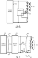
- Fig. 5 is a simplified circuit diagram of an output stage 501 of an exemplary driver device for semiconductor light sources such as LEDs 102.
- An internal bus voltage of the driver device appears between an upper rail 403 and a lower rail 404.
- the output stage has essentially the topology of a buck converter of the low side switch type, so that a power switch 502 is between a freewheeling current loop (comprising the LEDs 102, an inductor 503, and a freewheeling diode 504) and the lower rail 404 of the bus voltage.
- the first part of the output current path comes from the upper (positive) rail 403 of the internal bus voltage and comprises, in this order, a coupling to the first electrode of the output capacitance 409 at point 505, the first switch 408 (here: a MOSFET of the p-channel type), and the first node 406 of the output.
- the second part of the output current path comprises, in this order, the second node 407 of the output and a coupling to the second electrode of the output capacitance 409 at point 506.
- the first electrode of the output capacitance 409 is directly connected to the upper rail 403 of the bus voltage in fig. 5 .
- the inductor 503 As well as the power switch 502 and parallel to it a series connection of a resistor 507 and capacitor 508. These constitute sufficient electric coupling so that the bus voltage Vbus gets to charge the output capacitance 409 even when the power switch 502 is not conductive.
- the control input of the first switch 408 is its gate electrode, to which a control circuit 509 is coupled through a first driver circuit 510.
- the role of the first driver circuit 510 is to deliver the driving pulses to the control input of the first switch 408 at a suitable polarity, amplitude, and slew rate; the origin of the driving pulses is preferably in the control circuit 509, so in the following we may pay most attention to the role and actions of the control circuit 509.
- the control circuit 509 is configured to selectively open and close the first switch 408 by producing (or unambiguously causing the production of) the appropriate driving pulses and providing them (with the help of the first driver circuit 510) to the control input of the first switch 408.
- the control circuit 509 is configured to implement a closing sequence in closing the first switch 408.
- the closing sequence consists of a series of closing pulses that become longer towards the end of the closing sequence.
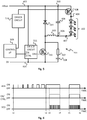
- Fig. 6 illustrates an example of the on/off switching of the first switch 408, the value of the control signal to the second driver circuit 511, and the switching pulses to the power switch 502.
- time t1 both the first switch 408 and the power switch 502 in the buck converter are open, and even if the output capacitance 409 is fully charged no current flows through the LEDs 102 and no light is consequently emitted.
- the closing sequence takes place between times t1 and t2.
- the first switch 408 has a characteristic turn-on time, which according to the established terminology of semiconductor technology is the time between the moment when a closing pulse to its gate begins and the moment when the conductivity of the channel between its drain and source has reached 90% of its maximum value.
- the channel of the first switch 408 conducts some current but presents a considerable resistance.
- the first pulse (or a number of first pulses) in the closing sequence are not long enough to make the first switch 408 fully conductive.
- an electric current of a smaller amplitude makes it through the first switch 408 during the first pulse (or a number of first pulses) in the closing sequence than if the switch 408 had been closed at once, or if each pulse in the closing sequence would have been long enough to make the switch 408 fully conductive.
- control circuit 509 is also responsible for selectively enabling and disabling the operation of the buck converter in fig. 5 . This is accomplished by utilizing an enabling input or control input in the second driver circuit 511, which second driver circuit repeatedly switches the power switch 502 on and off when the converting of the internal bus voltage to the output voltage is enabled by the control circuit 509.
- an enabling input or control input in the second driver circuit 511 which second driver circuit repeatedly switches the power switch 502 on and off when the converting of the internal bus voltage to the output voltage is enabled by the control circuit 509.
- the control circuit 509 is configured to provide an active level signal to the enabling input of the second driver circuit 511. In fig. 6 this happens at time t3, and the active level signal lasts until time t4. Since the operation of the buck converter is enabled for this duration, the power switch 502 receives repeated switching pulses from the second driver circuit 511, as seen on the lowest time axis in fig. 6 . The frequency and duty cycle of those switching pulses depend e.g. on the current control scheme that the buck converter employs, and is of minor importance here - output current monitoring has been left out from the simplified circuit diagram of fig. 5 in order to preserve graphical clarity.
- the control circuit 509 is configured to close the first switch 408 in accordance with said closing sequence before enabling the buck converter (or more generally: the switched-mode power supply) to begin the converting of the internal bus voltage to the output voltage.
- the first switch 408 remains conductive but the enabling signal to the second driver circuit 511 (and thus also the switching pulses to the power switch 502) has not yet begun.
- This interval can be considered as a safety margin ensuring that the closing sequence used to close the first switch 408 has ended, the charging state of the output capacitance 409 has stabilized, and the first switch 408 is certainly conductive at the moment when the buck converter is activated.
- This kind of an additional interval is not necessarily needed; in an alternative embodiment the enabling signal to the second driver circuit 511 can begin immediately at the same moment when the closing sequence ends, so t2 may be the same as t3.
- Fig. 6 also shows an example of how the control circuit 509 is configured to perform pulse width modulation of the output current of the driver device by repeatedly enabling and disabling the conversion of the internal bus voltage to the output voltage (the middle time axis in fig. 6 ) and by repeatedly closing and opening the first switch 408 in concert with said repeated enabling and disabling.
- the enabling signal goes inactive, ending the provision of switching pulses to the power switch, and also the first switch 408 goes off.
- the enabling signal goes active, beginning anew the provision of switching pulses to the power switch, and also the first switch 408 goes on again, only to be opened once more at time t6 when also the operation of the buck converter is halted again.
- the duration of the period t4-t5 is so short that the output capacitance 409 does not become fully charged, or it does not become charged to an extent that would again cause a large current spike at moment t5.
- the PWM frequency the frequency of the pulses on the middle time axis in fig. 6
- said period has a maximum duration way less than one millisecond.
- the length of the current decreasing period may be significant in comparison to the length of the PWM pulse, so the length of the actual PWM pulse would not correspond to the effective output current (and thus the effective light level perceived by the user) as accurately as desired.
- Opening the first switch 408 cuts the "tail" of the output current pulse and thus enhances accuracy.
- any PWM frequency used to dim LED lighting should be high enough in order to avoid perceivable flicker.
- the limit of acceptable PWM frequency depends on modulation depth, so that for example the so-called Lehman-Wilkins graph recommends setting the lower limit at 1.2 kHz for 100% flicker and accepting 100 Hz at about 2.5% flicker, with log-log interpolation between these two points.
- the rate at which the closing pulses occur during the closing sequence should be higher than 1 kHz.
- the resolution at which the pulses of the closing sequence become longer towards the end of the closing sequence may be quite fine, depending on the capability of the control circuit 509. As an example, if the internal clock frequency of the control circuit 509 is in the order of 50 MHz, each increasing step in pulse length may be in the order of 20 nanoseconds. This feature makes the use of a closing sequence as explained above easy to adapt to driver devices of various kinds, because it is not necessary to know exactly and/or beforehand, what will be the length of the characteristic turn-on time of the component that will be used as the first switch 408.
- the closing sequence may begin with pulses that are certainly shorter than any characteristic turn-on time of any typical switching component used in output stages of driver devices, so that when the pulses become longer towards the end of the closing sequence, their length will inevitably take the switching component through its resistive mode at some point.
- the lower limit of pulse length in the closing sequence is of the order of one clock cycle in the control circuit 509: for example a clock frequency in the order of 50 MHz sets the lower limit as 20 nanoseconds.
- As an upper limit of the pulse length it can be thought that they cannot at least be longer than the PWM pulses. If the PWM frequency is not lower than 1.2 kHz, corresponding to the cycle time of approximately 830 microseconds, and dimming down to 1% should be achieved, one PWM pulse may have e.g. the length 8,3 microseconds, which is thus an upper limit for the length of an individual pulse in the closing sequence as well.
- the closing sequence has only some tens of pulses, beginning from only some tens of nanoseconds and reaching a longest pulse length of some hundreds of nanoseconds, and the frequency of pulses in the closing sequence is hundreds of kHz, the closing sequence does not necessarily take longer than some tens of microseconds.
- the shortest pulse length may be considerably longer, like some hundreds of nanoseconds, in which case also the longest pulse length eventually arrived at may be in the order of microseconds.
- the closing sequence may comprise hundreds, thousands, or even hundreds of thousands of pulses.
- An upper limit for the duration of the closing sequence may come from the fact that the need to activate the output stage of a driver device may be a consequence of a user changing the setting of a dimmer. Users are typically quite anxious to see their actions affecting the lighting, so the delay before the lights actually begin to change should not be more than some seconds. Thus the duration of the closing sequence should be less than, say, one second. Closing sequences of even longer duration are possible if one does not need to consider the effects of the resulting delay in making changes to the characteristics of light.
- Fig. 7 illustrates timing of certain signals in a case in which an analogue control signal to the second driver circuit 511 is used in the same way as in the known CCR dimming of fig. 2 .
- the closing sequence between moments t1 and t2, and the safety margin of keeping the first switch 408 closed between moments t2 and t3, are the same as in fig. 6 .
- the second driver circuit 511 is enabled by raising the analogue control signal from zero to some relatively small value, corresponding to a relatively low dimming level.
- the internal control loop of the second driver circuit 511 applies a correspondingly small reference value to determine the maximum allowable measured current, which results in a relatively small duty cycle of the switching pulses to the power switch 502.
- the level of the analogue control signal gets higher, meaning that brighter light is required, and correspondingly the duty cycle of the power switch 502 becomes larger.
- Fig. 8 illustrates an alternative to the embodiment of fig. 7 .
- the first switch 408 performs PWM dimming by repeatedly cutting the main current path as instructed by the control signal it receives from the control circuit 509 (through the driver circuit 510).
- This embodiment involves the advantage that the smallest constant current level to which the lowest level of the analogue control signal to the second driver circuit 511 corresponds can still be kept sufficiently high to prevent e.g. colour distortions that could otherwise occur in the LEDs due to the small magnitude of current, and still the required very low dimming level can be achieved through the PWM dimming performed by the first switch 408.
- Some driver circuits of switched-mode power supplies have the special feature of accepting both analogue control signals and digital enabling pulses as inputs through a common input pin. This feature is found in many commercially available driver circuits, an example of which is the MP24894 manufactured by Monolithic Power Systems, San Jose, California. According to the circuit manufacturer the MP24894 can be made to apply a variable maximum current limit by coupling between its control input pin and ground pin a voltage that is at least 0.3V but less than 2.7V. The circuit manufacturer has meant that digital low/high pulses (0V / 3V) applied to the same input would act as disabling/enabling pulses that implement PWM control.
- a driver circuit of this kind can be controlled with pulses that have an amplitude between 0.3V and 2.7V to implement both CCR dimming and PWM dimming, so that the on-time of a pulse is the enabling period during which the output channel produces an output current according to the PWM principle, while the amplitude of the pulse determines the maximum value of output current that it may produce during that pulse.
- Fig. 9 illustrates timing of certain signals when the second driver circuit 502 is of the kind described above.
- the closing sequence between moments t1 and t2 is again the same as in figs. 6 to 8 , as is the safety margin between moments t2 and t3, if one is considered advantageous.
- enabling pulses of a relatively small amplitude are given to the second driver circuit 502.
- the amplitude of the enabling pulses is small in order to make the second driver circuit apply a relatively small reference value to determine the maximum allowable measured current during the intervals when it is enabled.
- the duty cycle of the power switch 502 is very small during the enabling pulses in the control signal, and the power switch remains completely non-conductive between the enabling pulses.
- the main current path is repeatedly cut with the first switch 408 in concert with disabling the second driver circuit 511. Between moments t4 and t5 pure CCR dimming is applied, by gradually changing the level of the control signal to the second driver circuit 511 while keeping the second driver circuit 511 enabled all the time. The results are seen as the increasingly larger duty cycle of the switching action of the power switch 502.
- the first switch 408 can be kept continuously closed after moment t4.
- a driver device with two or more parallel output channels that share a common control circuit.
- a driver device can be used to drive for example tunable white lighting, so that a first output channel is coupled to produce output current to warm white LEDs, a second output channel is coupled to produce output current to cold white LEDs, and the common control circuit controls the relative intensities of the warm and cold white LEDs to produce white light of desired colour temperature.
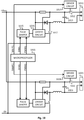
- Fig. 10 illustrates a simplified circuit diagram of a two-channel driver device for semiconductor light sources.
- the first channel is in the upper part of the drawing, above the microprocessor 1001 that constitutes the control circuit for both channels.
- the output current path of the first channel is divided into a first part and a second part by a two-pole output connector 1011, showing a tangible example of an output for semiconductor light sources.
- a controllable first switch 1012 is located in the first part of said output current path in the same way as the p-channel MOSFET in fig. 5 .
- An output capacitance 1013 is coupled across the output, with the first switch 1012 located between one electrode of the output capacitance 1013 and the corresponding node of the output.
- the controlling microprocessor 1001 is coupled to a control input of the first switch 1012 through a driver circuit 1014 and is configured to selectively open and close the first switch 1012, in particular in accordance with a closing sequence consisting of a series of closing pulses that become longer towards the end of the closing sequence.
- the second channel is in the lower part of fig. 10 .
- the output current path of the second channel is divided into a first part and a second part by a two-pole output connector 1021.
- the connectors 1011 and 1021 may physically appear together as a common connector with at least four poles, or they may be separate connectors.
- a controllable second switch 1022 is located in the first part of the output current path of the second channel, and an output capacitance 1023 is coupled across the output, with the second switch 1022 located between one electrode of the output capacitance 1023 and the corresponding node of the output.
- Closing the second switch 1022 enables a discharging current to flow to the output capacitance 1023 of the second channel if semiconductor light sources are in place and bridge the output connector 1021, completing the current path for the discharging current.
- the controlling microprocessor 1001 is coupled to the control input of the second switch 1022 through a driver circuit 1024 and is configured to selectively open and close the second switch 1022, in particular in accordance with a closing sequence consisting of a series of closing pulses that become longer towards the end of the closing sequence.
- the controlling microprocessor 1001 may be configured to implement the closing sequence in closing any of the first switch 1012 and the second switch 1022 when the output current of the respective output channel is switched on after a period of having been off.
- Such a situation may arise for example when the colour (or colour temperature) of the emitted light has been at one extreme value, so that only the LEDs of the other channel have emitted light, and the user or a device that produces lighting effects gives a command to gradually begin changing the colour (or colour temperature) towards a blended tone.
- This may be described in other words as changing the colour or colour temperature of light by initiating the flow of output current through semiconductor light sources of particular emission spectrum, wherein said initiating comprises implementing said closing sequence of a controllable switch on the output current path coupled to said semiconductor light sources of particular emission spectrum
- the signal that goes from the controlling microprocessor 1001 to the driver circuit 1014 is labelled RAMP1 (correspondingly RAMP2 for the second output channel) in fig. 10 and it may come in any of a number of formats. For example, it may be a train of pulses that directly constitute the closing sequence, so that the role of the driver circuit 1014 is only to take care that the corresponding pulses are directed to the first switch 1012 at suitable polarity, amplitude, and slew rate. This is a straightforward option, because the relatively high clock frequency of the controlling microprocessor 1001 (typically in the order of at least tens of MHz) enables it to time any of its digital output signals at considerable resolution.
- RAMP1 correspondingly RAMP2 for the second output channel
- the signals RAMP1 and RAMP2 could be for example analogue voltage values, with some unequivocal correspondence to desired switching pulse durations, so that the driver circuits 1014 and 1024 would be responsible for producing the corresponding pulses that constituted the closing sequence.
- Both output channels in fig. 10 are of the type described earlier with reference to fig. 9 : each power switch has a respective driver circuit that obeys both analogue and digital control signals.
- the controlling microprocessor 1001 produces two output signals labelled DIM1 and PWM1 (correspondingly: DIM2 and PWM2 for the second output channel) in fig. 10 .
- the DIM1 signal is an analogue signal that defines a reference or maximum current level
- the PWM1 pulse is a digital signal that defines an enabling period. Both signals go to a pulse shaper 1015, which produces control pulses so that their duration (or duty cycle) corresponds to the PWM1 signal and their amplitude corresponds to the DIM1 signal.
- control pulses are conducted to a suitable input pin of the second driver circuit 1016 which then operates accordingly, producing the switching pulses to the power switch 1017.
- a similar structure appears in the lower output channel in fig. 10 with output signals DIM2 and PWM2 controlling its operation.
- any measuring of currents for the purpose of controlling the operation of the driver device can be made in many other ways than the ones described above and in the drawings.
- the concept of using a closing sequence can be applied regardless of whether the switch on the current path is on the anode side or the cathode side of the LEDs.
- Components that have been illustrated as discrete components may be combined into integrated circuits in various ways.
Landscapes
- Circuit Arrangement For Electric Light Sources In General (AREA)
- Led Devices (AREA)
Claims (13)
- Dispositif d'attaque (401) destiné à des sources lumineuses à semi-conducteurs (102), comprenant :- un trajet de courant de sortie, divisé en une première partie et une seconde partie par une sortie pour lesdites sources lumineuses à semi-conducteurs, ladite sortie comprenant un premier noeud (406) et un second noeud (407),- un premier commutateur contrôlable (408) sur ledit trajet de courant de sortie, couplé à un dudit premier noeud (406) et dudit second noeud (407),- une capacitance de sortie (409) couplée à ladite sortie et audit premier commutateur (408) de sorte que fermer ledit premier commutateur (408) permet à un courant de décharge de circuler à partir de ladite capacitance de sortie (409) à travers les sources lumineuses à semi-conducteurs (102) couplées entre lesdits premier et second noeuds (406, 407),- un circuit de commande (509) couplé par le biais d'un premier circuit d'attaque (510) à une entrée de commande dudit premier commutateur (408) et configuré pour ouvrir et fermer sélectivement ledit premier commutateur (408), et- une alimentation électrique en mode commuté (405) couplée à ladite sortie et configurée pour convertir une tension de bus interne (Vbus) dudit dispositif d'attaque (401) en une tension de sortie (Vout) afin de commander un courant de sortie à travers lesdites sources lumineuses à semi-conducteurs (102) couplées entre lesdits premier et second noeuds (406, 407) ;caractérisé en ce que ledit circuit de commande (509) est configuré pour ouvrir et fermer sélectivement ledit premier commutateur (408) en fonction des impulsions définies par une séquence de fermeture avant de permettre à ladite alimentation électrique en mode commuté (405) de commencer ladite conversion de la tension de bus interne (Vbus) en tension de sortie (Vout), dans lequel ladite séquence de fermeture se compose d'une série d'impulsions de fermeture qui deviennent plus longues vers la fin de la séquence de fermeture, la séquence de fermeture fournissant ainsi les sources lumineuses à semi-conducteurs (102) couplées entre lesdits premier et second noeuds (406, 407) avec une protection contre un courant transitoire.
- Dispositif d'attaque selon la revendication 1, dans lequel :- ledit premier commutateur est un transistor à effet de champ ayant un temps d'activation de caractéristiques, et- au moins une première impulsion dans ladite séquence de fermeture est plus courte que ledit temps d'activation de caractéristiques.
- Dispositif d'attaque selon la revendication 1 ou la revendication 2, dans lequel un taux auquel se produisent lesdites impulsions de fermeture pendant ladite séquence de fermeture est supérieur à 1 kHz, et dans lequel une durée de la séquence de fermeture est inférieure à 1 seconde.
- Dispositif d'attaque selon la revendication 3, dans lequel le taux auquel se produisent lesdites impulsions de fermeture pendant ladite séquence de fermeture est supérieur à 100 kHz, et dans lequel la durée de la séquence de fermeture est inférieure à 2 millisecondes.
- Dispositif d'attaque selon l'une quelconque des revendications précédentes, dans lequel ladite alimentation électrique en mode commuté comprend un commutateur de puissance (502) et un circuit d'attaque de commande de courant (511) configuré pour commuter de manière répétée ladite commutation de puissance sur marche et arrêt lorsque ladite conversion de la tension de bus interne en tension de sortie est activée par ledit circuit de commande.
- Dispositif d'attaque selon la revendication 5, dans lequel ledit circuit de commande est configuré pour exécuter une modulation de largeur d'impulsion du courant de sortie en activant et en désactivant de manière répétée la conversion de la tension de bus interne en tension de sortie, et en fermant et en ouvrant de manière répétée ledit premier commutateur en concert avec ladite activation et désactivation répétées.
- Dispositif d'attaque selon l'une quelconque des revendications 5 à 6, dans lequel :- ladite alimentation électrique en mode commuté est un convertisseur abaisseur du type de commutateur côté bas, de sorte que ledit commutateur de puissance se trouve entre une boucle de courant en roue libre et un rail inférieur de la tension de bus interne du dispositif d'attaque.
- Dispositif d'attaque selon l'une quelconque des revendications précédentes, dans lequel la première partie dudit trajet de courant de sortie vient d'un rail positif de la tension de bus interne du dispositif d'attaque et comprend, dans cet ordre :- un couplage à une première électrode de ladite capacitance de sortie,- ledit premier commutateur, et- le premier noeud de ladite sortie,et dans lequel la seconde partie dudit trajet de courant de sortie comprend, dans cet ordre :- le second noeud de ladite sortie et- un couplage à une seconde électrode de ladite capacitance de sortie.
- Dispositif d'attaque selon l'une quelconque des revendications précédentes, dans lequel :- ledit trajet de courant de sortie est le trajet de courant de sortie d'un premier canal de sortie du dispositif d'attaque,- le dispositif d'attaque comprend, en plus dudit premier canal de sortie, un second canal de sortie, dont le trajet de courant de sortie comprend un second commutateur contrôlable,- ladite capacitance de sortie est la capacitance de sortie dudit premier canal de sortie, et le dispositif d'attaque comprend également une capacitance de sortie dudit second canal de sortie, couplée à une sortie dudit second canal de sortie et audit second commutateur de sorte que fermer ledit second commutateur permet à un courant de décharge de circuler de ladite capacitance de sortie du second canal de sortie à travers des sources lumineuses à semi-conducteurs couplées à la sortie dudit second canal de sortie,- le circuit de commande est également couplé à une entrée de commande dudit second commutateur et configuré pour ouvrir et fermer sélectivement ledit second commutateur, et- le circuit de commande est configuré pour ouvrir et fermer sélectivement l'un quelconque dudit premier commutateur et dudit second commutateur en fonction des impulsions définies par ladite séquence de fermeture lorsque le courant de sortie du canal de sortie respectif est allumé après une période où il a été éteint.
- Procédé de production d'un courant de sortie pour des sources lumineuses à semi-conducteurs (102) couplées entre un premier noeud (406) et un second noeud (407) d'un trajet de courant de sortie, dans lequel un premier commutateur contrôlable (408) couplé à un desdits premier et second noeuds (406, 407) est disposé dans ledit trajet de courant de sortie et dans lequel une capacitance de sortie (409) est couplée entre lesdits premier et second noeuds (406, 407) et audit premier commutateur (408) de sorte que fermer ledit premier commutateur (408) permet à un courant de décharge de circuler à partir de ladite capacitance de sortie (409) à travers lesdites sources lumineuses à semi-conducteurs (102), caractérisé en ce que le procédé comprend, dans l'ordre suivant, de :- conserver ouvert le premier commutateur (408) pour empêcher le courant de sortie de circuler, et- ouvrir et fermer de manière répétée ledit premier commutateur (408) en fonction d'impulsions définies par une séquence de fermeture, dans laquelle le fait de fermer des impulsions devient plus long vers la fin de la séquence de fermeture, ce qui permet de décharger graduellement ladite capacitance de sortie (409) et ainsi de fournir les sources lumineuses à semi-conducteurs (102) couplées entre lesdits premier et second noeuds (406, 407) avec une protection contre un courant transitoire.
- Procédé selon la revendication 10, dans lequel un transistor à effet de champ ayant un temps d'activation de caractéristiques est utilisé en tant que ledit premier commutateur, et au moins la première impulsion dans ladite séquence de fermeture est plus courte que ledit temps d'activation de caractéristiques.
- Procédé selon la revendication 10 ou 11, comprenant après ladite séquence de fermeture, dans l'ordre suivant, de :- maintenir ledit premier commutateur fermé pour permettre au courant de sortie de circuler,- démarrer une alimentation électrique en mode commuté pour convertir une tension de bus interne en une tension de sortie afin de commander le courant de sortie à travers lesdites sources lumineuses à semi-conducteurs, et- activer et désactiver de manière répétée la conversion de la tension de bus interne en tension de sortie, et fermer et ouvrir de manière répétée ledit premier commutateur en concert avec lesdites activation et désactivation répétées, pour produire un courant de sortie modulé en largeur d'impulsion.
- Procédé selon l'une quelconque des revendications 10 à 12, comprenant :- le changement de la couleur ou de la température de la couleur de lumière en initiant le flux du courant de sortie à travers des sources lumineuses à semi-conducteurs d'un spectre d'émission particulier, dans lequel ladite initiation comprend la mise en oeuvre de ladite séquence de fermeture dudit premier commutateur sur le trajet de courant de sortie couplée auxdites sources lumineuses à semi-conducteurs d'un spectre d'émission particulier.
Priority Applications (1)
| Application Number | Priority Date | Filing Date | Title |
|---|---|---|---|
| EP17158632.4A EP3370479B1 (fr) | 2017-03-01 | 2017-03-01 | Procédé et circuit pour protéger des leds de courants transitoires |
Applications Claiming Priority (1)
| Application Number | Priority Date | Filing Date | Title |
|---|---|---|---|
| EP17158632.4A EP3370479B1 (fr) | 2017-03-01 | 2017-03-01 | Procédé et circuit pour protéger des leds de courants transitoires |
Publications (2)
| Publication Number | Publication Date |
|---|---|
| EP3370479A1 EP3370479A1 (fr) | 2018-09-05 |
| EP3370479B1 true EP3370479B1 (fr) | 2019-10-02 |
Family
ID=58192236
Family Applications (1)
| Application Number | Title | Priority Date | Filing Date |
|---|---|---|---|
| EP17158632.4A Active EP3370479B1 (fr) | 2017-03-01 | 2017-03-01 | Procédé et circuit pour protéger des leds de courants transitoires |
Country Status (1)
| Country | Link |
|---|---|
| EP (1) | EP3370479B1 (fr) |
Families Citing this family (2)
| Publication number | Priority date | Publication date | Assignee | Title |
|---|---|---|---|---|
| CN110045199B (zh) * | 2019-03-20 | 2024-05-03 | 杭州通鉴科技有限公司 | 一种eft/esd/cs电磁干扰分析仪 |
| CN113872774B (zh) * | 2021-09-06 | 2023-10-24 | 波达通信设备(广州)有限公司 | 一种poe电源控制电路及供电方法 |
Family Cites Families (5)
| Publication number | Priority date | Publication date | Assignee | Title |
|---|---|---|---|---|
| WO2011039678A1 (fr) * | 2009-09-30 | 2011-04-07 | Koninklijke Philips Electronics N.V. | Gradation d'intensité de circuit d'attaque de del |
| JP5182400B2 (ja) * | 2010-08-24 | 2013-04-17 | カシオ計算機株式会社 | 半導体光源装置及び半導体光源制御方法 |
| EP2538753A1 (fr) * | 2011-06-21 | 2012-12-26 | Helvar Oy Ab | Dispositif de commande pour DEL et procédé pour la fourniture de courant électrique à des DEL |
| JP6086005B2 (ja) * | 2012-09-20 | 2017-03-01 | カシオ計算機株式会社 | 駆動装置、発光装置及び投影装置 |
| US9596728B2 (en) * | 2015-05-29 | 2017-03-14 | Linear Technology Corporation | Maintaining output capacitance voltage in LED driver systems during PWM off times |
-
2017
- 2017-03-01 EP EP17158632.4A patent/EP3370479B1/fr active Active
Non-Patent Citations (1)
| Title |
|---|
| None * |
Also Published As
| Publication number | Publication date |
|---|---|
| EP3370479A1 (fr) | 2018-09-05 |
Similar Documents
| Publication | Publication Date | Title |
|---|---|---|
| CN102724792B (zh) | 用于led组件的控制单元以及照明系统 | |
| EP2334146B1 (fr) | Circuit de commande pour diodes électroluminescentes | |
| EP2123128B1 (fr) | Circuit d'attaque pour charges telles qu'une del, une oled ou des diodes laser | |
| US8692481B2 (en) | Dimmer-controlled LEDs using flyback converter with high power factor | |
| US7919928B2 (en) | Boost LED driver not using output capacitor and blocking diode | |
| EP2214457B1 (fr) | Appareil de gradation de del | |
| JP5047373B2 (ja) | Led調光装置 | |
| CN101779522B (zh) | 具有旁路驱动的led装置 | |
| US10051704B2 (en) | LED dimmer circuit and method | |
| US11284488B2 (en) | Circuit assembly and method for operating an LED module | |
| US9155150B2 (en) | LED driver operating in different modes | |
| EP3370479B1 (fr) | Procédé et circuit pour protéger des leds de courants transitoires | |
| US9992826B1 (en) | Dual mode constant current LED driver | |
| EP3016478B1 (fr) | Commande combinée de la puissance de sortie dans un pilote de DEL multicanal | |
| EP3451798B1 (fr) | Circuit d'alimentation électrique et système d'éclairage et procédé pour faire fonctionner un circuit d'alimentation électrique | |
| EP3621411A1 (fr) | Ensemble circuit et procédé pour faire fonctionner un module de del | |
| EP3821683B1 (fr) | Circuits de commande et procédés d'excitation d'au moins un groupe de del |
Legal Events
| Date | Code | Title | Description |
|---|---|---|---|
| PUAI | Public reference made under article 153(3) epc to a published international application that has entered the european phase |
Free format text: ORIGINAL CODE: 0009012 |
|
| STAA | Information on the status of an ep patent application or granted ep patent |
Free format text: STATUS: THE APPLICATION HAS BEEN PUBLISHED |
|
| AK | Designated contracting states |
Kind code of ref document: A1 Designated state(s): AL AT BE BG CH CY CZ DE DK EE ES FI FR GB GR HR HU IE IS IT LI LT LU LV MC MK MT NL NO PL PT RO RS SE SI SK SM TR |
|
| AX | Request for extension of the european patent |
Extension state: BA ME |
|
| STAA | Information on the status of an ep patent application or granted ep patent |
Free format text: STATUS: REQUEST FOR EXAMINATION WAS MADE |
|
| 17P | Request for examination filed |
Effective date: 20190305 |
|
| RBV | Designated contracting states (corrected) |
Designated state(s): AL AT BE BG CH CY CZ DE DK EE ES FI FR GB GR HR HU IE IS IT LI LT LU LV MC MK MT NL NO PL PT RO RS SE SI SK SM TR |
|
| GRAP | Despatch of communication of intention to grant a patent |
Free format text: ORIGINAL CODE: EPIDOSNIGR1 |
|
| STAA | Information on the status of an ep patent application or granted ep patent |
Free format text: STATUS: GRANT OF PATENT IS INTENDED |
|
| INTG | Intention to grant announced |
Effective date: 20190417 |
|
| GRAS | Grant fee paid |
Free format text: ORIGINAL CODE: EPIDOSNIGR3 |
|
| GRAA | (expected) grant |
Free format text: ORIGINAL CODE: 0009210 |
|
| STAA | Information on the status of an ep patent application or granted ep patent |
Free format text: STATUS: THE PATENT HAS BEEN GRANTED |
|
| AK | Designated contracting states |
Kind code of ref document: B1 Designated state(s): AL AT BE BG CH CY CZ DE DK EE ES FI FR GB GR HR HU IE IS IT LI LT LU LV MC MK MT NL NO PL PT RO RS SE SI SK SM TR |
|
| REG | Reference to a national code |
Ref country code: GB Ref legal event code: FG4D |
|
| REG | Reference to a national code |
Ref country code: CH Ref legal event code: EP Ref country code: AT Ref legal event code: REF Ref document number: 1187678 Country of ref document: AT Kind code of ref document: T Effective date: 20191015 |
|
| REG | Reference to a national code |
Ref country code: DE Ref legal event code: R096 Ref document number: 602017007370 Country of ref document: DE |
|
| REG | Reference to a national code |
Ref country code: IE Ref legal event code: FG4D |
|
| REG | Reference to a national code |
Ref country code: DE Ref legal event code: R079 Ref document number: 602017007370 Country of ref document: DE Free format text: PREVIOUS MAIN CLASS: H05B0033080000 Ipc: H05B0045000000 |
|
| REG | Reference to a national code |
Ref country code: NL Ref legal event code: MP Effective date: 20191002 |
|
| REG | Reference to a national code |
Ref country code: LT Ref legal event code: MG4D |
|
| REG | Reference to a national code |
Ref country code: AT Ref legal event code: MK05 Ref document number: 1187678 Country of ref document: AT Kind code of ref document: T Effective date: 20191002 |
|
| PG25 | Lapsed in a contracting state [announced via postgrant information from national office to epo] |
Ref country code: SE Free format text: LAPSE BECAUSE OF FAILURE TO SUBMIT A TRANSLATION OF THE DESCRIPTION OR TO PAY THE FEE WITHIN THE PRESCRIBED TIME-LIMIT Effective date: 20191002 Ref country code: LV Free format text: LAPSE BECAUSE OF FAILURE TO SUBMIT A TRANSLATION OF THE DESCRIPTION OR TO PAY THE FEE WITHIN THE PRESCRIBED TIME-LIMIT Effective date: 20191002 Ref country code: PL Free format text: LAPSE BECAUSE OF FAILURE TO SUBMIT A TRANSLATION OF THE DESCRIPTION OR TO PAY THE FEE WITHIN THE PRESCRIBED TIME-LIMIT Effective date: 20191002 Ref country code: AT Free format text: LAPSE BECAUSE OF FAILURE TO SUBMIT A TRANSLATION OF THE DESCRIPTION OR TO PAY THE FEE WITHIN THE PRESCRIBED TIME-LIMIT Effective date: 20191002 Ref country code: BG Free format text: LAPSE BECAUSE OF FAILURE TO SUBMIT A TRANSLATION OF THE DESCRIPTION OR TO PAY THE FEE WITHIN THE PRESCRIBED TIME-LIMIT Effective date: 20200102 Ref country code: FI Free format text: LAPSE BECAUSE OF FAILURE TO SUBMIT A TRANSLATION OF THE DESCRIPTION OR TO PAY THE FEE WITHIN THE PRESCRIBED TIME-LIMIT Effective date: 20191002 Ref country code: PT Free format text: LAPSE BECAUSE OF FAILURE TO SUBMIT A TRANSLATION OF THE DESCRIPTION OR TO PAY THE FEE WITHIN THE PRESCRIBED TIME-LIMIT Effective date: 20200203 Ref country code: NO Free format text: LAPSE BECAUSE OF FAILURE TO SUBMIT A TRANSLATION OF THE DESCRIPTION OR TO PAY THE FEE WITHIN THE PRESCRIBED TIME-LIMIT Effective date: 20200102 Ref country code: GR Free format text: LAPSE BECAUSE OF FAILURE TO SUBMIT A TRANSLATION OF THE DESCRIPTION OR TO PAY THE FEE WITHIN THE PRESCRIBED TIME-LIMIT Effective date: 20200103 Ref country code: LT Free format text: LAPSE BECAUSE OF FAILURE TO SUBMIT A TRANSLATION OF THE DESCRIPTION OR TO PAY THE FEE WITHIN THE PRESCRIBED TIME-LIMIT Effective date: 20191002 Ref country code: ES Free format text: LAPSE BECAUSE OF FAILURE TO SUBMIT A TRANSLATION OF THE DESCRIPTION OR TO PAY THE FEE WITHIN THE PRESCRIBED TIME-LIMIT Effective date: 20191002 Ref country code: NL Free format text: LAPSE BECAUSE OF FAILURE TO SUBMIT A TRANSLATION OF THE DESCRIPTION OR TO PAY THE FEE WITHIN THE PRESCRIBED TIME-LIMIT Effective date: 20191002 |
|
| PG25 | Lapsed in a contracting state [announced via postgrant information from national office to epo] |
Ref country code: RS Free format text: LAPSE BECAUSE OF FAILURE TO SUBMIT A TRANSLATION OF THE DESCRIPTION OR TO PAY THE FEE WITHIN THE PRESCRIBED TIME-LIMIT Effective date: 20191002 Ref country code: HR Free format text: LAPSE BECAUSE OF FAILURE TO SUBMIT A TRANSLATION OF THE DESCRIPTION OR TO PAY THE FEE WITHIN THE PRESCRIBED TIME-LIMIT Effective date: 20191002 Ref country code: IS Free format text: LAPSE BECAUSE OF FAILURE TO SUBMIT A TRANSLATION OF THE DESCRIPTION OR TO PAY THE FEE WITHIN THE PRESCRIBED TIME-LIMIT Effective date: 20200224 Ref country code: CZ Free format text: LAPSE BECAUSE OF FAILURE TO SUBMIT A TRANSLATION OF THE DESCRIPTION OR TO PAY THE FEE WITHIN THE PRESCRIBED TIME-LIMIT Effective date: 20191002 |
|
| PG25 | Lapsed in a contracting state [announced via postgrant information from national office to epo] |
Ref country code: AL Free format text: LAPSE BECAUSE OF FAILURE TO SUBMIT A TRANSLATION OF THE DESCRIPTION OR TO PAY THE FEE WITHIN THE PRESCRIBED TIME-LIMIT Effective date: 20191002 |
|
| REG | Reference to a national code |
Ref country code: DE Ref legal event code: R097 Ref document number: 602017007370 Country of ref document: DE |
|
| PG2D | Information on lapse in contracting state deleted |
Ref country code: IS |
|
| PG25 | Lapsed in a contracting state [announced via postgrant information from national office to epo] |
Ref country code: RO Free format text: LAPSE BECAUSE OF FAILURE TO SUBMIT A TRANSLATION OF THE DESCRIPTION OR TO PAY THE FEE WITHIN THE PRESCRIBED TIME-LIMIT Effective date: 20191002 Ref country code: EE Free format text: LAPSE BECAUSE OF FAILURE TO SUBMIT A TRANSLATION OF THE DESCRIPTION OR TO PAY THE FEE WITHIN THE PRESCRIBED TIME-LIMIT Effective date: 20191002 Ref country code: DK Free format text: LAPSE BECAUSE OF FAILURE TO SUBMIT A TRANSLATION OF THE DESCRIPTION OR TO PAY THE FEE WITHIN THE PRESCRIBED TIME-LIMIT Effective date: 20191002 Ref country code: IS Free format text: LAPSE BECAUSE OF FAILURE TO SUBMIT A TRANSLATION OF THE DESCRIPTION OR TO PAY THE FEE WITHIN THE PRESCRIBED TIME-LIMIT Effective date: 20200202 |
|
| PLBE | No opposition filed within time limit |
Free format text: ORIGINAL CODE: 0009261 |
|
| STAA | Information on the status of an ep patent application or granted ep patent |
Free format text: STATUS: NO OPPOSITION FILED WITHIN TIME LIMIT |
|
| PG25 | Lapsed in a contracting state [announced via postgrant information from national office to epo] |
Ref country code: SK Free format text: LAPSE BECAUSE OF FAILURE TO SUBMIT A TRANSLATION OF THE DESCRIPTION OR TO PAY THE FEE WITHIN THE PRESCRIBED TIME-LIMIT Effective date: 20191002 Ref country code: IT Free format text: LAPSE BECAUSE OF FAILURE TO SUBMIT A TRANSLATION OF THE DESCRIPTION OR TO PAY THE FEE WITHIN THE PRESCRIBED TIME-LIMIT Effective date: 20191002 Ref country code: SM Free format text: LAPSE BECAUSE OF FAILURE TO SUBMIT A TRANSLATION OF THE DESCRIPTION OR TO PAY THE FEE WITHIN THE PRESCRIBED TIME-LIMIT Effective date: 20191002 |
|
| 26N | No opposition filed |
Effective date: 20200703 |
|
| PG25 | Lapsed in a contracting state [announced via postgrant information from national office to epo] |
Ref country code: MC Free format text: LAPSE BECAUSE OF FAILURE TO SUBMIT A TRANSLATION OF THE DESCRIPTION OR TO PAY THE FEE WITHIN THE PRESCRIBED TIME-LIMIT Effective date: 20191002 |
|
| REG | Reference to a national code |
Ref country code: CH Ref legal event code: PL |
|
| PG25 | Lapsed in a contracting state [announced via postgrant information from national office to epo] |
Ref country code: SI Free format text: LAPSE BECAUSE OF FAILURE TO SUBMIT A TRANSLATION OF THE DESCRIPTION OR TO PAY THE FEE WITHIN THE PRESCRIBED TIME-LIMIT Effective date: 20191002 |
|
| REG | Reference to a national code |
Ref country code: BE Ref legal event code: MM Effective date: 20200331 |
|
| PG25 | Lapsed in a contracting state [announced via postgrant information from national office to epo] |
Ref country code: LU Free format text: LAPSE BECAUSE OF NON-PAYMENT OF DUE FEES Effective date: 20200301 |
|
| PG25 | Lapsed in a contracting state [announced via postgrant information from national office to epo] |
Ref country code: IE Free format text: LAPSE BECAUSE OF NON-PAYMENT OF DUE FEES Effective date: 20200301 Ref country code: CH Free format text: LAPSE BECAUSE OF NON-PAYMENT OF DUE FEES Effective date: 20200331 Ref country code: FR Free format text: LAPSE BECAUSE OF NON-PAYMENT OF DUE FEES Effective date: 20200331 Ref country code: LI Free format text: LAPSE BECAUSE OF NON-PAYMENT OF DUE FEES Effective date: 20200331 |
|
| PG25 | Lapsed in a contracting state [announced via postgrant information from national office to epo] |
Ref country code: BE Free format text: LAPSE BECAUSE OF NON-PAYMENT OF DUE FEES Effective date: 20200331 |
|
| GBPC | Gb: european patent ceased through non-payment of renewal fee |
Effective date: 20210301 |
|
| PG25 | Lapsed in a contracting state [announced via postgrant information from national office to epo] |
Ref country code: GB Free format text: LAPSE BECAUSE OF NON-PAYMENT OF DUE FEES Effective date: 20210301 |
|
| PG25 | Lapsed in a contracting state [announced via postgrant information from national office to epo] |
Ref country code: TR Free format text: LAPSE BECAUSE OF FAILURE TO SUBMIT A TRANSLATION OF THE DESCRIPTION OR TO PAY THE FEE WITHIN THE PRESCRIBED TIME-LIMIT Effective date: 20191002 Ref country code: MT Free format text: LAPSE BECAUSE OF FAILURE TO SUBMIT A TRANSLATION OF THE DESCRIPTION OR TO PAY THE FEE WITHIN THE PRESCRIBED TIME-LIMIT Effective date: 20191002 Ref country code: CY Free format text: LAPSE BECAUSE OF FAILURE TO SUBMIT A TRANSLATION OF THE DESCRIPTION OR TO PAY THE FEE WITHIN THE PRESCRIBED TIME-LIMIT Effective date: 20191002 |
|
| PG25 | Lapsed in a contracting state [announced via postgrant information from national office to epo] |
Ref country code: MK Free format text: LAPSE BECAUSE OF FAILURE TO SUBMIT A TRANSLATION OF THE DESCRIPTION OR TO PAY THE FEE WITHIN THE PRESCRIBED TIME-LIMIT Effective date: 20191002 |
|
| REG | Reference to a national code |
Ref country code: DE Ref legal event code: R081 Ref document number: 602017007370 Country of ref document: DE Owner name: HELVAR COMPONENTS OY AB, FI Free format text: FORMER OWNER: HELVAR OY AB, ESPOO, FI |
|
| PGFP | Annual fee paid to national office [announced via postgrant information from national office to epo] |
Ref country code: DE Payment date: 20260327 Year of fee payment: 10 |