EP3373085B1 - Ensemble circuit à entrée multifonction, en particulier pour l'unité électronique de commande et de régulation d'un groupe motopompe - Google Patents
Ensemble circuit à entrée multifonction, en particulier pour l'unité électronique de commande et de régulation d'un groupe motopompe Download PDFInfo
- Publication number
- EP3373085B1 EP3373085B1 EP18000245.3A EP18000245A EP3373085B1 EP 3373085 B1 EP3373085 B1 EP 3373085B1 EP 18000245 A EP18000245 A EP 18000245A EP 3373085 B1 EP3373085 B1 EP 3373085B1
- Authority
- EP
- European Patent Office
- Prior art keywords
- input
- voltage
- digital
- signal
- switch
- Prior art date
- Legal status (The legal status is an assumption and is not a legal conclusion. Google has not performed a legal analysis and makes no representation as to the accuracy of the status listed.)
- Active
Links
Images




Classifications
-
- G—PHYSICS
- G05—CONTROLLING; REGULATING
- G05B—CONTROL OR REGULATING SYSTEMS IN GENERAL; FUNCTIONAL ELEMENTS OF SUCH SYSTEMS; MONITORING OR TESTING ARRANGEMENTS FOR SUCH SYSTEMS OR ELEMENTS
- G05B19/00—Program-control systems
- G05B19/02—Program-control systems electric
- G05B19/04—Program control other than numerical control, i.e. in sequence controllers or logic controllers
- G05B19/042—Program control other than numerical control, i.e. in sequence controllers or logic controllers using digital processors
- G05B19/0423—Input/output
-
- F—MECHANICAL ENGINEERING; LIGHTING; HEATING; WEAPONS; BLASTING
- F04—POSITIVE - DISPLACEMENT MACHINES FOR LIQUIDS; PUMPS FOR LIQUIDS OR ELASTIC FLUIDS
- F04D—NON-POSITIVE-DISPLACEMENT PUMPS
- F04D15/00—Control, e.g. regulation, of pumps, pumping installations or systems
-
- F—MECHANICAL ENGINEERING; LIGHTING; HEATING; WEAPONS; BLASTING
- F04—POSITIVE - DISPLACEMENT MACHINES FOR LIQUIDS; PUMPS FOR LIQUIDS OR ELASTIC FLUIDS
- F04D—NON-POSITIVE-DISPLACEMENT PUMPS
- F04D15/00—Control, e.g. regulation, of pumps, pumping installations or systems
- F04D15/0088—Testing machines
-
- G—PHYSICS
- G05—CONTROLLING; REGULATING
- G05B—CONTROL OR REGULATING SYSTEMS IN GENERAL; FUNCTIONAL ELEMENTS OF SUCH SYSTEMS; MONITORING OR TESTING ARRANGEMENTS FOR SUCH SYSTEMS OR ELEMENTS
- G05B2219/00—Program-control systems
- G05B2219/20—Pc systems
- G05B2219/21—Pc I-O input output
- G05B2219/21085—Define type of I-O, analog, digital, pulse
-
- G—PHYSICS
- G05—CONTROLLING; REGULATING
- G05B—CONTROL OR REGULATING SYSTEMS IN GENERAL; FUNCTIONAL ELEMENTS OF SUCH SYSTEMS; MONITORING OR TESTING ARRANGEMENTS FOR SUCH SYSTEMS OR ELEMENTS
- G05B2219/00—Program-control systems
- G05B2219/20—Pc systems
- G05B2219/21—Pc I-O input output
- G05B2219/21114—Universal input, AC or DC
-
- G—PHYSICS
- G05—CONTROLLING; REGULATING
- G05B—CONTROL OR REGULATING SYSTEMS IN GENERAL; FUNCTIONAL ELEMENTS OF SUCH SYSTEMS; MONITORING OR TESTING ARRANGEMENTS FOR SUCH SYSTEMS OR ELEMENTS
- G05B2219/00—Program-control systems
- G05B2219/30—Nc systems
- G05B2219/32—Operator till task planning
- G05B2219/32141—Define type of I-O, analog, digital, pulse
Definitions
- the present invention relates to a circuit arrangement of a control device for technical building equipment, in particular for the control and regulation electronics of a pump unit, for processing an output signal of a device, with a multifunctional input comprising two connections for connecting the device.
- the invention relates to an input for connecting various sensors of different sensor types to the control device.
- the invention further relates to a method for determining which type of device is connected to the circuit arrangement.
- EP 2461221 A2 a control unit for headlight range control for headlights that require the inclination of the vehicle body.
- the determination of the angle of inclination of the vehicle is made possible by an analog sensor or a PWM sensor, whereby the control unit has a changeable wiring of the sensor input and is therefore set up to process the sensor signals of both types of sensors.
- Building automation control devices often have control or regulation functions that rely on a measurement signal from a specific sensor or an external control signal, for example as a setpoint, from another building automation device, for example a higher-level control component.
- the sensor or other device must then be connected to the control device and delivers a corresponding output signal, which in the case of the sensor is a measurement signal and in the case of another device is generally a control signal.
- the sensors can be, for example, a pressure or differential pressure sensor, volume flow sensor, temperature sensor, humidity sensor, brightness sensor, vibration sensor, current sensor, speed sensor or any other sensor.
- Modern centrifugal pump units for heating, cooling or drinking water systems have control and regulation electronics that can be operated in a variety of different control types and require a variety of different sensors for this.
- differential temperature control requires the connection of two temperature sensors, unless a temperature sensor is already integrated into the pump.
- Other types of control such as differential pressure control or volume flow control require different input signals in order to obtain a setpoint from an external building management system.
- the device types that output a current unit signal or voltage unit signal are active devices or sensors, meaning they do not need to be supplied with a current or voltage from the control device.
- passive sensors that require an appropriate supply voltage or current. This is the case, for example, with so-called resistance thermometers (thermistors), whose resistance changes depending on the ambient temperature. Examples are an NTC, PTC or a platinum temperature sensor (PT1000).
- the temperature to be determined is here determined via a resistance measurement based on the characteristic curve of the corresponding resistance thermometer.
- the control and regulation electronics of centrifugal pump units for heating, cooling or drinking water systems usually have analog 0V... 10V or 4mA...20mA inputs. If a temperature sensor needs to be connected here, this requires the use of an additional converter, which converts the temperature measurement signal into a 4-20mA value, for example.
- the aforementioned device types provide an analog measurement signal.
- devices that deliver a digital measurement signal include devices whose output signal is a square wave signal of a certain frequency and amplitude, whereby the duty cycle, i.e. the time ratio of high and low within a period, indicates a value between 0% and 100%.
- the maximum value of 100% and the minimum value of 0% cannot be achieved for technical reasons.
- Another type of digital sensor is a so-called 1-wire sensor, which has a data connection for serially sending and receiving digital data and is also supplied with a supply voltage via this.
- connection terminal In order to be able to connect the different types of sensors and devices to the building automation control unit, a separate connection terminal is usually required and provided in the control unit for each type of signal, i.e. voltage signal, current signal, thermistor voltage, PWM, 1-wire data. If more than one device/sensor of a certain type is to be connected, there must be a corresponding number of connection terminals. It follows from this that a relatively large number of connection terminals are required in total in order to ensure the greatest possible flexibility with regard to the connection options for sensors and external control devices.
- connection terminals each require appropriate installation space, so that the connection areas of the control devices are comparatively large.
- connection terminals due to the large number of connection options, there is a risk that connection terminals will be confused. This can not only cause malfunctions control unit, it can also lead to damage or destruction of the connected sensor/device or an electronic component of the control unit connected to the corresponding connection terminal.
- a circuit arrangement for a control device for technical building equipment in particular for a control and regulation unit of a pump unit, for processing an output signal of a device, is proposed, which has a multifunctional input comprising two connections for connecting the device and can be operated in at least two different modes . At least three different types of devices with output signals of different types can be connected to the input, the circuit arrangement having an internal wiring of the input with at least one controllable switch for changing the internal wiring depending on the type of device connected.
- connection terminals Due to the circuit arrangement according to the invention, it is no longer necessary to provide a separate input on the control device for each of the different device types.
- the number of inputs can be reduced to one multifunctional input or, if necessary, several of these inputs, so that the space required for connection terminals that make the input accessible is reduced to one Minimum is reduced and it is impossible to mix up a connection terminal.
- the devices that can be connected can be sensors whose output signal represents a measurement signal, or another external control device, for example a building management system, whose output signal is a control signal, which sends a setpoint to the control device with its output signal, for example.
- the multifunctional input is preferably only formed by the two connections, so that the devices to be connected can only be connected via two wires or lines.
- One connection is suitably connected to ground, while the actual output signal is transmitted via the other connection.
- the internal circuitry of the multifunctional input directs the output signal, depending on the device type-dependent configuration, to other components of the circuit arrangement in order to make it usable for its intended purpose.
- the circuit arrangement can be operable in at least three different modes, in which at least the three different device types can be connected to the input, the internal circuitry having more than one controllable switch in order to change its configuration depending on the connected device type.
- one of the modes in which the circuit arrangement can be operated can be a voltage mode, in which a device with a voltage signal as an output signal can be connected to the input, an analog-digital converter being connected to the input in order to detect the voltage signal.
- the analog-digital converter thus forms part of the circuit arrangement according to the invention. It processes the voltage signal present at the input by digitizing it and making it available for further processing in a digital control or regulation.
- the analog-digital converter can be connected directly to the multifunctional input. However, it makes sense before analog-digital Arrange a low-pass filter on the converter to suppress measurement noise.
- the output voltage of the low-pass filter can be limited to the maximum input voltage of the analog-to-digital converter in order to protect it from overvoltage. It is also advantageous if a voltage divider is arranged between the analog-digital converter and the input, in particular between the low-pass filter and the input, in order to adapt the voltage signal to the measuring range of the analog-digital converter. Low-pass filters and voltage dividers then also form components of the circuit arrangement.
- the voltage signal can be a voltage unit signal, for example for the voltage ranges of 0V-5V, 0-10V, 1V-5V, 2V to 10V or - 10V to + 10V.
- the device in voltage mode can be a sensor, with the output signal forming a measurement signal, or an external control device, with the output signal forming a control signal, in particular for specifying the setpoint.
- one of the modes in which the circuit arrangement can be operated can be a current mode, in which a device with a current signal as an output signal can be connected to the input, and in which a load resistor that can be switched on with a switch connects the input to ground and an analog-to-digital converter is connected to the input to detect a voltage drop across the load resistor.
- the analog-digital converter also forms part of the circuit arrangement according to the invention, as does the load resistor and the switch.
- the load resistor can be switched on or off using the switch, which can be controlled here, with switching on meaning connecting to ground so that it becomes electrically effective. Switching off, however, renders the load resistor ineffective.
- the connection to ground can be made directly or indirectly via at least one further electrical or electronic component.
- the switch can be a controllable semiconductor switch, for example a transistor, in particular a MOSFET.
- the current signal coming via the input flows through the load resistor to ground, creating a voltage drop across the load resistor.
- This one will measured by the analog-digital converter. It therefore processes the voltage signal present at the input by digitizing it and making it available for further processing in a digital control or regulation.
- the analog-to-digital converter here is identical to the one used in voltage mode, including its optional connection through the low pass and the voltage divider.
- the circuit arrangement according to the invention can be operated alternatively in the voltage mode and the current mode, it makes sense if the two analog-digital converters of the two modes are formed by one and the same analog-digital converter. The number of components, the installation space and the complexity of the circuit arrangement are thereby reduced.
- the current signal can be a current unit signal, for example for the current ranges 0-20mA or 4-20mA.
- the device in current mode can be a sensor, with the output signal forming a measurement signal, or an external control device, with the output signal forming a control signal, in particular for specifying the setpoint.
- one of the modes in which the circuit arrangement can be operated is a temperature mode in which a resistance thermometer can be connected to the input, and in which a current source that can be switched on with a switch is used to supply the resistance thermometer with a measuring current and generate a voltage signal as an output signal with the Input is connected, and an analog-to-digital converter is connected to the input to record the voltage across the resistance thermometer.
- the analog-digital converter forms part of the circuit arrangement according to the invention, as does the power source and the switch.
- the power source can be switched on or off, or switched on or off based on the multifunctional input, whereby switching on means connecting to the input and switching off means disconnecting the connection of the input to the power source.
- the switch can be a controllable semiconductor switch, for example a transistor, in particular a MOSFET.
- the current coming from the power source flows via the multifunctional input to the resistance thermometer and creates a voltage drop there. This is measured by the analog-digital converter. It processes the voltage signal present at the input by digitizing it. In order to determine the temperature, the resistance value of the resistance thermometer must then be determined.
- the circuit arrangement can be set up accordingly, with the measured voltage value at the input being divided by the current supplied by the power source. According to a variant, the current can be assumed to be known, in particular if the current source is designed as a constant current source.
- the circuit arrangement knows the characteristic curve of the resistance thermometer, so that it can determine the temperature from this characteristic curve based on the resistance value.
- the circuit arrangement can have a control unit and a memory, and can also be set up accordingly in terms of programming.
- the control unit can be, for example, a microcontroller, an FPGA (Field Programmable Gate Array) or an ASIC (Application-Specific Integrated Circuit).
- analog-to-digital converter here is identical to the one used in voltage mode. With regard to its optional wiring through the low pass and the voltage divider, this also applies, but only to the extent that the voltage divider must be able to be switched off in this case and in particular must be switched off so that the current from the power source is not divided between the voltage divider and the resistance thermometer and thus the measuring current through the resistance thermometer would be unequal to the current of the power source.
- this circuitry is required for the voltage divider of the analog-digital converter in the voltage and/or current mode in order not to make the measurement in the temperature mode distort, at least if a voltage divider is present.
- the analog-digital converter is therefore preferably connected to the input via a voltage divider that can be switched off with a switch, the voltage divider being switched off in the mode with a resistance thermometer connected.
- the switch can be designed as a controllable semiconductor switch, in particular as a transistor, in particular a MOSFET. For example, the switch disconnects the voltage divider from ground.
- the analog-digital converter used in the temperature mode is preferably a different analog-digital converter than in the voltage mode or current mode.
- the circuit arrangement according to the invention can be operated either in the temperature mode and at least one of the voltage mode and current mode, the circuit arrangement thus comprises two analog-digital converters. This makes it possible to implement further improvements to the circuitry in order to achieve more precise measured values.
- the other analog-to-digital converter is suitably preceded by a low-pass filter in order to suppress measurement noise. However, it makes sense that it does not have a voltage divider.
- the power source is preferably only active in temperature mode, as it is not needed in one of the other modes and would also be annoying.
- the resistance thermometer can be a PT100, a PT1000, an NTC or PTC.
- a reference resistor can be located between the power source and the input. This enables an exact determination the current of the power source, as this can vary due to scatter and temperature drift.
- a high-precision reference resistor for example with a maximum tolerance of 0.1%, is preferably used here. This makes it possible to determine the temperature with an accuracy of none equal to 0.5K.
- a first analog-digital converter can be connected to the multifunctional input via the reference resistor, while a second analog-digital converter can be connected to the input to record the voltage across the resistance thermometer.
- the circuit arrangement can have a processor, in particular a microcontroller, FPGA or ASIC, and a memory and can also be set up accordingly in terms of programming.
- the first analog-digital converter can correspond to the previously described analog-digital converter of the voltage mode or current mode
- the second analog-digital converter corresponds to the other analog-digital converter previously described for the temperature mode. It is ideal if the second analog-to-digital converter is connected to a node between the load resistor and the switch that can connect the load resistor to ground. This has the advantage that the second analog-digital converter can also be usefully used in current mode, namely here to measure a voltage drop across the switch, which falsifies the voltage across the load resistor measured by the first analog-digital converter. To improve the measurement accuracy in current mode, the voltage measured by the second analog-digital converter must then be subtracted from the voltage measured by the first analog-digital converter.
- the circuit arrangement can be set up accordingly for this purpose. The calculation can be carried out, for example, in the control unit, in particular the processor. The circuit arrangement can therefore be set up accordingly in terms of programming for this calculation.
- a protective diode can be arranged in front of or behind the switch.
- the node that leads to the second analog-digital converter is then preferably arranged between the series connection of protective diode and switch and the load resistor. This ensures that the voltage drop across the protective diode is also recorded by the second analog-digital converter and taken into account when correcting the measured value of the first analog-digital converter.
- the power source can be a constant current source.
- the current source for adjusting the level of the measuring current can be a controlled current source. This has the advantage that different resistance thermometers are used and the level of the current can be adjusted accordingly to the resistance thermometer used. Furthermore, drift effects can be compensated for by adjusting the level of the supply current.
- the power source can be controlled, for example, in a voltage-controlled manner.
- a digital-to-analog converter (DAC) can preferably be used for this, the output of which is connected to the control input of the power source.
- DAC digital-to-analog converter
- the current source can be regulated, being connected directly to the input with a feedback input via a feedback path.
- the feed current of the power source can be kept constant and temperature influences on the power source can be eliminated.
- the feedback ensures that the converter regulates the current so that the voltage across the externally connected resistance thermometer corresponds exactly to the voltage at the DAC output.
- the DAC output voltage is always set so that a current of 0.5mA passes through the reference resistor and that externally connected resistance thermometer flows.
- a constant current through the resistance thermometer ensures a constant voltage drop across the line and connection resistances and is noticeable as a constant offset over the entire temperature measuring range of the resistance thermometer. This constant offset can then be subtracted from the measured value in the software application.
- one of the modes in which the circuit arrangement can be operated can be a PWM mode, in which a device with a digital voltage signal of constant frequency indicating a duty cycle can be connected as an output signal to the input is.
- a device with a digital voltage signal of constant frequency indicating a duty cycle can be connected as an output signal to the input is.
- an analog-digital converter can be connected to the input via a low-pass filter.
- the PWM signal is a square-wave signal that transmits the setpoint information within a period via the duty cycle, i.e. the ratio of the time duration of high and low.
- the digital voltage signal (PWM signal) is thus fed to the low-pass filter, which supplies a direct voltage at its output that is proportional to the duty cycle and is measured by the analog-digital converter.
- the PWM signal is first converted into an analog signal and then digitized again.
- the information transported with the PWM signal, in particular a setpoint is thus retained and can be processed in the PWM mode of the circuit arrangement.
- the analog-digital converter here can correspond to the analog-digital converter as described previously for voltage mode or current mode.
- the analog-digital converter required in the PWM mode can be formed by the analog-digital converter from the voltage mode.
- the analog-digital converter required in the PWM mode can be formed by the first analog-digital converter from the temperature mode.
- the PWM signal is not processed via an analog-digital converter, but rather via a switchable digital input.
- This can be connected directly to the input if it has a very high resistance and therefore does not affect the accuracy of the analog measurement.
- the digital input can be connected to the input via a switch, whereby it is also connected to process the PWM signal according to this other variant.
- the digital input can be an input of a counter.
- the digital input is part of the circuit arrangement. For example, it forms an input of a control unit, for example a microprocessor or microcontroller, in which the analog-digital converter or converters are also formed.
- the switch can be a controllable semiconductor switch, for example a transistor, in particular a MOSFET.
- a MOSFET has the advantage that it is controlled without power and therefore has the lowest losses. It makes sense for the switch to connect the digital input to the multifunctional input via the voltage divider, so that the voltage divider adapts the PWM signal to the value range of the digital input.
- one of the modes in which the circuit arrangement can be operated can be a data mode in which a digital sensor that can be fed via a common data and supply line is connected to the input can be connected to a digital output signal.
- an operating voltage for the digital sensor that can be switched on with a switch is connected to the input via a bridgeable pull-up resistor. Also connected to the input is a digital input that can be switched on with a switch.
- the multifunctional input In the data mode, it is possible to process the data of a 1-wire sensor via the multifunctional input, which is powered via one and the same line and can transmit or receive data.
- the data is sent to the digital input and can be processed there directly.
- Digital input can be the same input or a different input than PWM mode. If it is the same digital input, the switch to connect the digital input to the multifunctional input is also the same as in PWM mode.
- the pull-up resistor is necessary to generate a low signal.
- Digital sensors often work with active-low signals, i.e. transmit a logical 1 as a low signal via the bus line. If no data is transferred, the pull-up resistor automatically pulls the bus line to high.
- the pull-up resistor can be bridged to trigger initialization of the sensor. Bridging can be done using a switch that connects the input directly to the supply voltage. Both this switch and the switch for the pull-up resistor and the switch for the digital input can be designed as controllable semiconductor switches, for example as transistors, in particular as MOSFETs. These switches as well as the pull-up resistor and the digital input form part of the circuit arrangement.
- the circuit arrangement is set up to be operated in at least three of these modes.
- a combination of optionally switchable modes means that the circuit arrangement includes all components that are described in relation to the respective mode.
- the circuit arrangement can be configured to be operated in one of the five modes. To enable this, it may include all of the components described above in relation to voltage mode, current mode, temperature mode, PWM mode and data mode.
- a control unit can be used, which itself forms part of the circuit arrangement according to the invention.
- the control unit can output control signals to turn the switch or switches on or off depending on the mode.
- the control inputs of the switches are connected to the control unit via appropriate control lines.
- the control unit can be formed, for example, by a processor, for example a microprocessor or microcontroller, an FPGA or ASIC.
- This control unit preferably also includes the analog-digital converter or the first and second analog-digital converters and/or the digital-analog converter.
- the configuration can, for example, be triggered manually by an operator of the control device by selecting the mode on the control device, i.e. essentially telling the control device which type of device is or should be connected to the input.
- the circuit arrangement is set up to automatically recognize which type of device is connected to the input. This can be determined, for example, based on the voltage present at the input and/or the frequency of the output signal and/or based on the input impedance of the connected device.
- the circuit arrangement can be set up accordingly to determine the device type based on the to determine the input voltage, frequency or input resistance of the device.
- the circuit arrangement can be set up to recognize the mode independently by successively switching the switches for switching the components of the internal circuit on and/or off.
- the switching on and/or off can be carried out programmatically by the control unit, whereby a corresponding program can be loaded onto the control unit and can run therein.
- the method for automatically determining the type of a device connected to the multifunctional input of a circuit arrangement according to the invention can be characterized in that the voltage, the frequency and / or the impedance is determined at the input and depending on the determined voltage, frequency and / or impedance on the Device type is closed.
- the voltage can be measured, for example, by an analog-digital converter.
- a digital counter can be used for the frequency.
- a device with a voltage signal, a device with a current signal and a resistance thermometer can be distinguished in a single step.
- the more different types of devices that can be connected to the multifunctional input the more complex it becomes. If a distinction is to be made between a device with a voltage signal and a device with a PWM signal, a further query is required. The same applies if a distinction is to be made between a resistance thermometer and a 1-wire sensor.
- the method may also include additional steps to issue error messages if, for example, no sensor is connected or an incorrect sensor is connected.
- the circuit arrangement immediately configures the internal circuitry of the input to the mode with the recognized device type. If necessary, the last switching state of all switches that led to the recognition of the device type can also be retained here.
- a device with a current signal is accepted as an output signal at the input if the voltage at the input is greater than an upper limit value.
- the maximum expected value of the voltage signal for example 10V
- a test of this assumption can be made by connecting a load resistor at the input to ground, inferring the device with the current signal if the voltage at the input is within a certain value range, or inferring a fault if it is not case is.
- the value range can be between 1.2V and 6V, for example.
- a device with a voltage signal as an output signal or a PWM device with a digital voltage signal of constant frequency indicating a duty cycle is accepted as an output signal at the input if the voltage at the input is between zero and an upper limit value .
- the maximum expected value of the voltage signal for example 10V, can be used as the upper limit value.
- the input can then be connected to a digital input, the frequency of the output signal can be determined and compared with a limit frequency. A conclusion can be drawn about the device using the voltage signal as an output signal if the determined frequency is below the limit frequency.
- the PWM device can be inferred if the determined frequency is above the cutoff frequency.
- a resistance thermometer or a 1-wire sensor is assumed at the input if there is no voltage at the input.
- the input can then be supplied with a supply voltage via a pull-up resistor.
- the supply voltage is, for example, 5V.
- the resistance thermometer is present if the voltage at the input is in a range of values below the supply voltage, for example between 0.5V and 1.5V.
- the 1-wire sensor is the same if the voltage at the input is equal to the supply voltage.
- an error can be concluded if the voltage at the input is outside the value range and is not equal to the supply voltage.
- the acceptance of a 1-wire sensor can be checked by connecting the input to a digital input, generating a specific voltage pulse sequence at the input as a request and waiting for a specific voltage pulse sequence as a response from the 1-wire sensor, with the 1-wire Sensor can be closed when the specific voltage pulse sequence is received in response. Alternatively, an error can be concluded if this is not the case, i.e. no response is received.
- the voltage pulse sequence forming the request at the input can be generated by pulsed connection of the input to ground, in particular the load resistor to ground.
- the circuit arrangement according to the invention is preferably set up to carry out the method.
- the process can be activated manually by an operator triggering a corresponding function on the control device. But it can also be activated automatically, for example when booting up (Booting) the control unit, or when an operator sets a specific control function in the control unit that requires a corresponding sensor or a setpoint at the multifunctional input.
- a further aspect of the invention relates to pump electronics for a pump unit with a circuit arrangement according to the invention.
- the pump electronics correspond to the control unit described here.
- a further aspect of the invention relates to a pump unit, in particular a centrifugal pump unit, with pump electronics which has a circuit arrangement according to the invention.
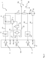
- Fig. 1 shows a first embodiment variant of a circuit arrangement 1 according to the invention for a control device for technical building equipment, in particular for control and regulation electronics of a pump unit.
- the circuit arrangement 1 has a multifunctional input 2 to which various devices 31, 32, 33, 34, here sensors, with different output signals I E , U E , U T , U PWM can be connected.
- the output signals can be viewed here as measurement or control signals.
- the input 2 consists of two connections 2a, 2b, of which a second connection 2b is connected to ground.
- the first connection 2a carries the actual output signal and is connected internally to process the output signal.
- the circuit arrangement 1 comprises a first analog-digital converter (ADC) 3, a first low-pass filter 11 and a voltage divider 6, the first ADC 3 is connected to the input 2 or the first connection 2a via the low-pass filter 11 and the voltage divider 6. These components form a primary measurement path 21.
- the voltage divider 6 is switchable and can be connected to ground by means of a first switch 7 in order to act in accordance with its intended purpose. If the first switch 7 is closed, the voltage divider 6 works as intended. If it is open, the voltage divider 6 has no effect.
- the first switch 7 is controlled via a control line 15 by a control unit 5 using the control signal EN_VD.
- the first ADC 3 is part of the control unit 5.
- the circuit arrangement 1 further comprises a switchable load resistor 8, typically with less than 300 ⁇ , which is connected with one of its connections to the first connection of the input 2.
- the load resistor 8 can be connected to ground with another connection. This is done with the help of a second switch 10. If the second switch 10 is closed, the load resistor 8 has an effect. If it is open, the load resistor 8 has no effect.
- the second switch 10 is controlled via a control line 16 by the control unit 5 using the control signal EN_RB.
- a second analog-digital converter (ADC) 4 is connected to the node between the load resistor 8 and the switch.
- a low-pass filter 14 is also connected upstream of this ADC 4.
- the second ADC 4 is also part of the control unit 5.
- the path from the input 2 to the second ADC 4 represents a secondary measurement path 22.
- the circuit arrangement 1 finally comprises a constant current source 12, a third switch 13 and a reference resistor 9, the current source 12 being connected to the input 2, in particular to its first connection 2a, via the reference resistor 9.
- the third switch 13 is here in series with the current source 12 and the reference resistor 9 and is connected between these two. In the closed state, the third switch 13 connects the current source 12 to the reference resistor 9; in the open state, the current source 12 is separated from the input 2.
- the third switch 13 can also be part of the power source 12 and switch it on and off.
- the third switch 13 is controlled via a control line 17 by the control unit 5 Control signal EN_CS.
- the reference resistor 9 is arranged so that it is also in series with the voltage divider, ie is part of the primary measuring path 21.
- the design variant according to can be connected to the multifunctional input 2 Fig. 1
- Four different devices 31, 32, 33, 34 can be connected, which are in Fig. 1 are shown on the right.
- a first device is a sensor 31, which delivers a voltage signal U E with values between 0... 10V.
- a second device is a sensor 32, which delivers a current signal I E with values between 4...20mA.
- a third device is a temperature sensor 33, in particular a PT1000, which must be supplied with a current I T and then delivers a measuring voltage U T.
- a fourth device is a PWM sensor 34, which provides a digital voltage signal U PWM , which is a square wave signal of constant frequency, the duty cycle, ie the ratio of the time duration of high and low within a period, having a value between 0% and 100 % depicts.
- the circuit arrangement can then be operated in a respective mode, in particular a measuring mode, of which there are a total of four here.
- the mode is set by the control unit 5.
- One of the modes is a voltage mode in which the device 31 with the voltage signal U E can be connected to the input 2.
- the first ADC 3 with active voltage divider 6 is used to reduce the voltage present at input 2 to determine voltage.
- the second and third switches 10, 13 are switched off.
- the voltage is then filtered by the low pass 11 after the voltage divider 6 and digitized at the first ADC 3 in the control unit 5.
- One of the modes is a current mode in which the device 32 with the current signal I E as an output signal can be connected to the input 2.
- the second switch 10 connects the load resistor 8 and the input 2 to ground.
- the current present at the input is converted into a voltage via the load resistor.
- the first ADC 3 is connected to the input 2 when the voltage divider 6 is active in order to detect a voltage drop across the load resistor 8.
- the voltage at input 2 is then filtered by the low pass 11 after the voltage divider 6 and digitized at the first ADC 3 in the control unit 5.
- a voltage drop across the second switch 10 is determined in the secondary measurement path 22 by the control unit 5 using the second ADC 4 via the second low pass 14. The voltage drop must be subtracted from the measured value of the first ADC 3.
- One of the modes is also a temperature mode in which the temperature sensor 33 (PT1000) can be connected to input 2.
- the circuitry is configured in such a way that the third switch 13 connects the power source 12 to the input 2 to supply the temperature sensor 33 with a measuring current via the reference resistor.
- the first switch 7 is open, so that the voltage divider 6 has no function.
- the second switch 10 is also open, so that the load resistor has no function.
- a current is impressed through the reference resistor 9 and the externally connected temperature sensor 33.
- a corresponding voltage U T is established at the input 2 depending on the temperature and thus the resistance of the temperature sensor 33. This is measured by the second ADC 4 in the control unit 5.
- the exact current I T that was impressed by the current source 12 must be determined. This results from the difference between the voltages measured by the first ADC 3 and the second ADC 4 (voltage drop across reference resistor 9) and the subsequent division by the value of the reference resistor 9.
- one of the modes is a PWM mode in which the PWM sensor 34 can be connected to input 2.
- the wiring of input 2 is identical to the voltage mode. So the first switch is closed, the second and third switches are open. However, it should be noted that the first switch can also be open, meaning that the entire voltage divider is not required if the PWM signal exceeds the voltage range of the ADC input. For example, this is the case if the voltage range of the ADC is between 0V and 3.3V and the PWM signal contains 5V or 10V pulses.
- the first ADC 3 is connected to the input 2 via the low pass 11 and the voltage divider 6.
- the PWM signal is thus converted by the low-pass filter 11 into an analog voltage, which is evaluated by the first ADC 3.
- the voltage is then proportional to the duty cycle of the PWM signal U PWM at the input.
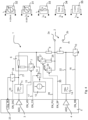
- Fig. 2 shows a second embodiment variant of a circuit arrangement 1 according to the invention.
- the power source 12 is now a regulated, voltage-controlled power source 12.
- a control input of the current source 12 is connected to the output of a digital-to-analog converter (DAC) 18, which is also part of the control unit 5.
- DAC digital-to-analog converter
- the voltage at the input 2 is fed back to an input of the current source 12 via a feedback path 19.
- a diode 20 is connected upstream of the second switch 10.
- the second switch preferably a transistor, for example a MOSFET, is connected by the diode D in front of negative Input voltages (in all measuring modes) and therefore effectively protected against destruction.
- Fig. 3 shows a third embodiment variant of a circuit arrangement 1 according to the invention. This differs from the first and second embodiment variants in that the control unit 5 has a digital input 23, which can be connected to the primary measuring path 21 and thus to the input 2 via a fourth switch 24.
- the fourth switch 24 is also controlled by the control unit 5 by a control signal EN_DIG.
- EN_DIG a control signal
- FIG. 3 An alternative configuration of the wiring of the multifunctional input 2 for PWM operation is possible. In this configuration, the first and fourth switches 7, 24 are on, the second and third switches 10, 13 are off. The first switch 7 only needs to be switched on when the PWM signal exceeds the voltage range of the digital input.
- the fourth switch 24 directs the PWM signal at input 2 to the digital input 23 and can be evaluated there immediately.
- Fig. 4 shows a fourth embodiment variant of a circuit arrangement 1 according to the invention, which is a further development of the third embodiment variant.
- This fourth variant can be operated in five different modes.
- one of the modes is a data mode in which a digital 1-wire sensor 35 with a digital output signal U 1W that can be fed via a common data and supply line can be connected to the input 2.
- a 1-wire sensor 35 can, for example, be a temperature sensor such as the DS18S20 from Maxim Integrated Products, Inc.
- An operating voltage VDD can be connected to the input 2 via a fifth switch 27 in order to power the 1-wire sensor 35.
- the operating voltage VDD is not connected directly to input 2, but rather via a pull-up resistor 26.
- the pull-up resistor can be bridged via a sixth switch 29. Both switches are controllable semiconductor switches that are controlled by the control unit 5, with the control signal EN_PU switching the fifth switch 28 (pull-up resistor) and the control signal EN_SP switching the sixth switch 29.
- Fig. 6 shows a flowchart of the method according to the invention for determining which type of device is connected to the multifunctional input 2.
- the method is program-controlled and implemented in the control unit 5, so that the circuit arrangement 1 is set up to automatically recognize which type of sensor or device type is connected to its input 2.
- the configuration of the circuitry required for the detected sensor or device is set immediately, or simply adopted, provided that the switch states were already set during the implementation of the method as they were required for the corresponding configuration.
- the method can be activated, for example, when starting up (booting) the control device, in particular the control device, or when switching on the control device.
- the process can be triggered manually in the control unit.
- it can be triggered automatically when a specific event occurs, for example when the user makes a control setting on the control unit that requires a specific sensor or setpoint at the multifunctional input.
- the device type is recognized by successively switching the switches to switch the components of the internal circuit on and/or off.
- step S1 The method begins in step S1 by ensuring that all switches 7, 10, 13, 24, 27, 29 are turned off.
- the control signal EN_VD is then first set to 1 and the first switch is activated so that the voltage divider 6 becomes active, step S2.
- step S2 is basically an optional step.
- the voltage at input 2 is then measured by the first analog-digital converter 3 and the device type is determined depending on the measured voltage, step S3.
- the more different types of devices that can be connected to the multifunctional input 2 become more complex. If a distinction is to be made between a device 31 with a voltage signal and a device 34 with a PWM signal, a further query is required. The same applies if a distinction is to be made between a resistance thermometer 33 and a 1-wire sensor 34.
- the method may also include steps or case distinctions S5, S13, S17 to issue error messages S7, S15 S19 when an abnormal condition has been detected at the input, indicating a missing sensor, a faulty sensor or an incorrect sensor.
- a device 32 with a current signal I E is assumed as an output signal at input 2 if the voltage at input 2 is greater than an upper limit value.
- the maximum expected value of the voltage signal for example 10V, can be used as the upper limit value.
- this assumption can also be checked for the recognized case "device 32 with current signal I E " by connecting the load resistor 8 at input 2 to ground, step S4.
- the signal EN_RB is set to 1 and the second switch 24 is activated.
- the voltage at input 2 is then measured again by the first ADC 3, step S5. If the voltage at input 2 reduces as expected to a certain value range, for example to a range between 1.2V and 6V, the assumption is confirmed and a device 32 with a current signal, for example a 0..20mA or 4.. .20mA sensor detected, step S6. Otherwise, an error is concluded, step S7 if this is not the case. An error message can then be displayed in particular.
- the senor is powered via a supply voltage, e.g. 24V.
- a device 31 with a voltage signal U E or a PWM device 34 with a PWM signal U PWM of a specific frequency at input 2 is assumed if the voltage at input 2 is between zero and the upper limit.
- the input 2 is then connected to the digital input 23, step S8.
- the EN_DIG signal is set to 1 and the fourth switch 24 is activated.
- the frequency of the output signal U ⁇ or U PWM is then determined and compared with a cutoff frequency, step S9.
- the device 31 with the voltage signal is then closed, step S10, if the determined frequency is below the limit frequency.
- the PWM device 34 is inferred if the determined frequency is above the cutoff frequency, step S11.
- the cutoff frequency is usefully below the frequency of the PWM signal, for example at 20Hz.
- the PWM signal has a frequency above the limit frequency and an amplitude that corresponds at most to the upper limit value (10V) based on the ground of input 2.
- a resistance thermometer 33 or a 1-wire sensor 35 is assumed at input 2 if there is no voltage at input 2.
- the input 2 is then supplied with the supply voltage VDD via the pull-up resistor 26 by setting the control signal EN_PU to 1 and the fifth switch 27 is closed, step S12.
- the supply voltage is, for example, 5V.
- the resistance thermometer 33 is then closed, step S14, if the voltage at input 2 is in a range of values below the supply voltage VDD, for example between 0.5V and 1.5V.
- the 1-wire sensor 35 is closed when the voltage at input 2 is almost equal to the supply voltage. If the voltage at the input is outside the value range and is not almost equal to the supply voltage, an error is concluded, step S15. An error message can then be displayed in particular.
- the acceptance of a 1-wire sensor 35 can be checked by connecting input 2 to digital input 23, step S16.
- the EN_DIG signal is set to 1 and the fourth switch 24 is activated.
- a specific voltage pulse sequence which represents a reset pulse, is generated at input 2, which is a request to sensor 35. This pulse is realized by switching on the second switch 10 in a correspondingly pulsed manner. The corresponding pulse sequence is represented in the signal EN_RB.
- the load resistor is connected to ground and input 2, to which the data line of the 1-wire sensor 35 is connected, is pulled to ground, i.e. an active low is transmitted.
- a specific voltage pulse sequence (presence pulse) is then waited for as a response from the 1-wire sensor 35. If the specific voltage pulse sequence is received as a response at digital input 23, step S17, it is confirmed that a 1-wire sensor 35 is connected to input 2, step S18. If there is no answer, it will closed to an error, step S19. An error message can then be displayed in particular.
- the circuit arrangement 1 is part of pump electronics of a pump unit, in particular a centrifugal pump unit.
- the pump electronics correspond to the control unit described here.
Landscapes
- Engineering & Computer Science (AREA)
- Mechanical Engineering (AREA)
- General Engineering & Computer Science (AREA)
- Physics & Mathematics (AREA)
- General Physics & Mathematics (AREA)
- Automation & Control Theory (AREA)
- Dc-Dc Converters (AREA)
- Electronic Switches (AREA)
- Arrangements For Transmission Of Measured Signals (AREA)
Claims (18)
- Circuit électronique de pompe d'une unité de pompage de l'équipement technique du bâtiment comprenant un arrangement de circuit (1) pour le traitement d'un signal de sortie (UE, IE, UT, UPWM, U1W) d'un appareil (31, 32, 33, 34, 35), avec une entrée multifonctionnelle (2) comprenant deux raccordements (2a, 2b) pour le raccordement de l'appareil (31, 32, 33, 34, 35), sachant que l'arrangement de circuit (1) peut fonctionner selon au moins deux modes différents, et qu'au moins trois types d'appareils différents peuvent être raccordés à l'entrée (2) avec des signaux de sortie de différents types, et un circuit interne de l'entrée (2) avec au moins un commutateur commandable (7, 10, 13, 24, 27) pour modifier le circuit interne en fonction du type d'appareil raccordé, et sachant que l'un des modes est un mode dans lequel un thermomètre PT100 ou PT1000 peut être raccordé à l'entrée (2) en tant que thermomètre à résistance (33), et dans lequel une source de courant (12) connectable par un commutateur (13) est reliée à l'entrée (2) pour alimenter le thermomètre à résistance (33) avec un courant de mesure et générer un signal de tension (UT) comme signal de sortie, et un convertisseur analogique-numérique (4) est relié à l'entrée (2) pour détecter la tension aux bornes du thermomètre à résistance (33).
- Circuit électronique de pompe selon la revendication 1, caractérisé en ce que- l'un des modes est un mode dans lequel un appareil (31) avec un signal de tension (Uε) peut être raccordé à l'entrée (2) comme signal de sortie, sachant qu'un convertisseur analogique-numérique (3) est relié à l'entrée (2, 2a) pour détecter le signal de tension (UE), et/ou- l'un des modes est un mode dans lequel un appareil (32) avec un signal de courant (IE) peut être raccordé à l'entrée (2) en tant que signal de sortie, et dans lequel une résistance de charge (8) pouvant être connectée à l'aide d'un commutateur (10) relie l'entrée (2, 2a) à la masse et un convertisseur analogique-numérique (3) est relié à l'entrée (2) afin de détecter une chute de tension aux bornes de la résistance de charge (8), et/ou- l'un des modes est un mode dans lequel un appareil (34) avec un signal de tension numérique (UPWM) de fréquence constante présentant un rapport cyclique peut être raccordé à l'entrée (2) en tant que signal de sortie, et en ce qu'un convertisseur analogique-numérique (3) est relié à l'entrée (2) par l'intermédiaire d'un filtre passe-bas (11) ou qu'une entrée numérique (23) pouvant être activée par un commutateur (24) est reliée à l'entrée (2), et/ou- que l'un des modes est un mode dans lequel un capteur numérique (35) pouvant être alimenté par l'intermédiaire d'une ligne de données et d'alimentation commune peut être raccordé à l'entrée (2) avec un signal de sortie numérique (U1W), et dans lequel une tension de service (VDD) pouvant être connectée au moyen d'un commutateur (27) pour le capteur numérique (35) est reliée à l'entrée (2) par l'intermédiaire d'une résistance pull-up (26) pouvant être pontée, et une entrée numérique (23) pouvant être connectée au moyen d'un commutateur (24) est reliée à l'entrée (2).
- Circuit électronique de pompe selon la revendication 2, caractérisé en ce qu'il est configurable pour fonctionner sélectivement dans l'un des modes mentionnés dans la revendication 2, sachant qu'il comprend de préférence une unité de commande (5) pour activer ou désactiver le ou les interrupteurs (7, 10, 13, 24, 27) en fonction du mode.
- Circuit électronique de pompe selon l'une des revendications 2 ou 3, caractérisé en ce que le convertisseur analogique-numérique (3) est relié à l'entrée (2, 2a) par l'intermédiaire d'un diviseur de tension (6) pouvant être mis hors circuit par un commutateur (7), sachant que le diviseur de tension est mis hors circuit dans le mode avec thermomètre à résistance (33) raccordée.
- Circuit électronique de pompe selon les revendications 2 à 4, caractérisé en ce qu'une résistance de référence (9) est située entre la source de courant (12) et l'entrée (2), sachant que le convertisseur analogique-numérique (4) destiné à détecter la tension aux bornes du thermomètre à résistance (33) est un deuxième convertisseur analogique-numérique (4) et un premier convertisseur analogique-numérique (3) est relié à l'entrée (2) par l'intermédiaire de la résistance de référence (9).
- Circuit électronique de pompe selon la revendication 5, caractérisé en ce que le deuxième convertisseur analogique-numérique (4) est relié à un noeud entre la résistance de charge (8) et le commutateur (10).
- Circuit électronique de pompe selon au moins la revendication 2, caractérisé en ce que la source de courant (12) est commandée en tension par un convertisseur numérique-analogique (18).
- Circuit électronique de pompe selon au moins la revendication 2 ou 7, caractérisé en ce que la source de courant (12) est régulée, sachant qu'elle est reliée directement à l'entrée (2) avec une entrée de rétroaction via un chemin de rétroaction (19).
- Circuit électronique de pompe au moins selon la revendication 3, caractérisé en ce que l'unité de commande (5) comprend le convertisseur analogique-numérique (3), le premier et le deuxième convertisseurs analogique-numérique (3, 4) et/ou le convertisseur numérique-analogique (18).
- Circuit électronique de pompe selon l'une des revendications précédentes, caractérisé en ce qu'il est agencé pour reconnaître de manière autonome quel type d'appareil est raccordé à l'entrée (2), sachant qu'il est de préférence agencé pour déterminer le type d'appareil raccordé à partir de la tension appliquée à l'entrée et/ou de la fréquence du signal de sortie (UE, IE, UT, UPWM, U1W) et/ou de l'impédance d'entrée de l'appareil raccordé (31, 32, 33, 34, 35), et/ou de reconnaître le type d'appareil par la commutation successive d'au moins un commutateur (10, 13, 24, 27) pour la mise en circuit et/ou hors circuit de composants du circuit interne.
- Procédé de détermination automatique du type d'un appareil (31, 32, 33, 34, 35) raccordé à l'entrée multifonctionnelle (2) d'un arrangement de circuit (1) d'un circuit électronique de pompe selon au moins l'une des revendications 1 à 10, sachant que la tension, la fréquence et/ou l'impédance à l'entrée (2) est déterminée et que le type d'appareil est déduit en fonction de la tension, de la fréquence et/ou de l'impédance déterminée, et un PT100 ou PT1000 est supposé être un thermomètre à résistance (33) ou un capteur 1 fil (35) à l'entrée (2) lorsqu'aucune tension n'est présente à l'entrée (2).
- Procédé selon la revendication 11, caractérisé en ce qu'après la reconnaissance du type d'appareil, le câblage interne est configuré sur le mode avec le type d'appareil reconnu.
- Procédé selon la revendication 11 ou 12, caractérisé en ce que- un appareil (32) avec un signal de courant (IE) est pris comme signal de sortie à l'entrée (2) lorsque la tension à l'entrée (2) est supérieure à une valeur limite supérieure, et/ou- qu'un appareil (31) avec un signal de tension (Uε) comme signal de sortie ou un appareil PWM (34) avec un signal de tension numérique (UPWM) de fréquence constante indiquant un rapport cyclique est supposé être le signal de sortie à l'entrée (2) lorsque la tension à l'entrée (2) est comprise entre zéro et une valeur limite supérieure.
- Procédé selon la revendication 13, caractérisé en ce qu"une vérification de l'hypothèse « Appareil (32) avec un signal de courant (IE) comme signal de sortie » est effectuée en reliant une résistance de charge (8) à l'entrée (2) à la masse, sachant qu'il est conclu sur l'appareil (32) avec le signal de courant (IE) si la tension à l'entrée (2) se trouve à l'intérieur d'une plage de valeurs déterminée, ou en concluant sinon à un défaut.
- Procédé selon la revendication 13 ou 14, caractérisé en ce que, dans le cas de l'hypothèse « Appareil (31) avec un signal de tension (UE) comme signal de sortie ou appareil PWM (34) avec signal de tension numérique (UPWM) », l'entrée (2) est ensuite reliée à une entrée numérique (23), la fréquence du signal de sortie est déterminée et comparée à une fréquence limite, sachant qu'il est déterminé sur l'appareil (31) avec le signal de tension (UE) comme signal de sortie si la fréquence déterminée est inférieure à la fréquence limite, ou sur l'appareil PWM (34) si la fréquence déterminée est supérieure à la fréquence limite.
- Procédé selon la revendication 13, 14 ou 15, caractérisé en ce que, dans le cas de l'hypothèse « Thermomètre à résistance (33) ou capteur 1 fil (35) », l'entrée est ensuite alimentée en tension d'alimentation (VDD) par l'intermédiaire d'une résistance pull-up (26), sachant qu'il est déterminé sur la sonde à résistance (33), si la tension à l'entrée (2) se situe dans une plage de valeurs inférieure à la tension d'alimentation (VDD), ou sur le capteur 1 fil (35) si la tension à l'entrée (2) est égale à la tension d'alimentation, ou sur un défaut si la tension à l'entrée (2) se situe en dehors de la plage de valeurs et n'est pas égale à la tension d'alimentation.
- Procédé selon l'une des revendications 13 à 16, caractérisé en ce qu'une vérification de l'acceptation d'un capteur 1 fil (35) est effectuée en reliant l'entrée (2) à une entrée numérique (23), en générant une certaine séquence d'impulsions de tension à l'entrée (2) en tant que demande et en attendant une certaine séquence d'impulsions de tension en tant que réponse du capteur 1 fil (35), sachant qu'il est déterminé sur le capteur 1 fil (35) si la certaine séquence d'impulsions de tension est reçu en tant que réponse ou qu'il est conclu à une erreur si ce n'est pas le cas.
- Procédé selon la revendication 17, caractérisé en ce que la séquence d'impulsions de tension formant la demande est générée à l'entrée (2) en reliant de manière pulsée l'entrée (2) à la terre, en particulier la résistance de charge (8) à la terre.
Applications Claiming Priority (1)
| Application Number | Priority Date | Filing Date | Title |
|---|---|---|---|
| DE102017002296.8A DE102017002296A1 (de) | 2017-03-11 | 2017-03-11 | Schaltungsanordnung mit multifunktionalem Eingang, insbesondere für die Steuer- und Regelelektronik eines Pumpenaggregats |
Publications (2)
| Publication Number | Publication Date |
|---|---|
| EP3373085A1 EP3373085A1 (fr) | 2018-09-12 |
| EP3373085B1 true EP3373085B1 (fr) | 2023-11-01 |
Family
ID=61827459
Family Applications (1)
| Application Number | Title | Priority Date | Filing Date |
|---|---|---|---|
| EP18000245.3A Active EP3373085B1 (fr) | 2017-03-11 | 2018-03-12 | Ensemble circuit à entrée multifonction, en particulier pour l'unité électronique de commande et de régulation d'un groupe motopompe |
Country Status (3)
| Country | Link |
|---|---|
| EP (1) | EP3373085B1 (fr) |
| CN (1) | CN108571451B (fr) |
| DE (1) | DE102017002296A1 (fr) |
Families Citing this family (1)
| Publication number | Priority date | Publication date | Assignee | Title |
|---|---|---|---|---|
| DE102019106566B3 (de) * | 2019-03-14 | 2020-09-10 | Samson Aktiengesellschaft | Konfiguration eines zweipoligen Eingangs |
Family Cites Families (6)
| Publication number | Priority date | Publication date | Assignee | Title |
|---|---|---|---|---|
| US5982290A (en) * | 1998-09-10 | 1999-11-09 | New Holland North America, Inc. | Automatic recognition of different types of liquid level sensors |
| US8140211B2 (en) * | 2008-01-22 | 2012-03-20 | GM Global Technology Operations LLC | Control module with flexible sensor inputs |
| US8326391B2 (en) * | 2008-03-12 | 2012-12-04 | General Electric Company | Sensor interface |
| JP5140113B2 (ja) * | 2010-05-10 | 2013-02-06 | 三菱電機株式会社 | 電子制御装置 |
| DE102010053304B4 (de) * | 2010-12-02 | 2012-08-02 | Automotive Lighting Reutlingen Gmbh | Steuergerät mit einem zur Verarbeitung von Signalen unterschiedlicher Sensortypen eingerichteten Eingang und Verfahren zum Anpassen eines Steuergeräts |
| EP3229085A1 (fr) * | 2016-04-05 | 2017-10-11 | Siemens Aktiengesellschaft | Circuit d'entree destine a la detection selective d'un signal analogique ou binaire |
-
2017
- 2017-03-11 DE DE102017002296.8A patent/DE102017002296A1/de not_active Withdrawn
-
2018
- 2018-03-12 CN CN201810201094.7A patent/CN108571451B/zh active Active
- 2018-03-12 EP EP18000245.3A patent/EP3373085B1/fr active Active
Also Published As
| Publication number | Publication date |
|---|---|
| CN108571451A (zh) | 2018-09-25 |
| EP3373085A1 (fr) | 2018-09-12 |
| CN108571451B (zh) | 2021-01-05 |
| DE102017002296A1 (de) | 2018-09-13 |
Similar Documents
| Publication | Publication Date | Title |
|---|---|---|
| CH686908A5 (de) | Verfahren zur Funktionskontrolle eines Temperaturfuehlers. | |
| DE102004022556B3 (de) | Selbstkalibrierende Vorrichtung zur Spannungsmessung und Verfahren hierfür | |
| EP4211518B1 (fr) | Dispositif de terrain pour automatisation à sécurité intrinsèque | |
| EP3111284B1 (fr) | Circuit d'entrée à redondance, unité de circuit d'entrée comprenant au moins un circuit d'entrée et procédé servant à faire fonctionner une unité de circuit d'entrée de ce type | |
| EP2550740B1 (fr) | Élément électronique pour un dispositif de capteur, dispositif de capteur et procédé de configuration d'un dispositif de capteur | |
| EP2176719B1 (fr) | Unité de bus de terrain pour un bus de terrain à deux fils | |
| EP3311503A1 (fr) | Dispositif de couplage d'appareil de terrain et système | |
| EP3373085B1 (fr) | Ensemble circuit à entrée multifonction, en particulier pour l'unité électronique de commande et de régulation d'un groupe motopompe | |
| EP3436834B1 (fr) | Agencement avec au moins deux unités d'entrée analogique redondantes pour un courant de mesure | |
| EP1593939B1 (fr) | Dispositif de capteur pour la mesure d'au moins un paramètre | |
| EP4139753A1 (fr) | Dispositif de terrain d'automatisation | |
| DE102005009593B4 (de) | Verfahren und Vorrichtung zum Einstellen der Ausgangsimpedanz einer Treiberstufe | |
| EP2603772B1 (fr) | Circuiterie de régulation et de surveillance d'un courant de signal et transducteur de mesure comprenant une telle circuiterie | |
| DE102018128305A1 (de) | Verfahren zur sensorseitigen Einstellung des vom Signaleingang einer übergeordneten Steuerungseinheit der Automatisierungstechnik erwarteten Signaltyps | |
| DE102014016852B4 (de) | Steuersystem für einen Elektromotor basierend auf einem gepulsten Steuersignal | |
| DE102008057725B4 (de) | System zum Abgleichen, Einstellen und/oder Programmieren von elektronischen Geräten, insbesondere Messgeräten, welche Sensoren aufweisen, sowie Schaltungsanordnung zum Abgleichen, Einstellen oder Programmieren von elektronischen Elementen, wie digitalen Potentiometern | |
| EP2335025B1 (fr) | Appareil de terrain pour l'automatisation de processus | |
| EP3602781B1 (fr) | Sélecteur de configuration et utilisateur de bus avec un tel sélecteur de configuration | |
| DE102004018533B4 (de) | Transistorbasierter Temperatursensor | |
| DE102014204039B3 (de) | Elektronisches Schaltgerät in Zweileitertechnik und Verfahren zum Betreiben eines solchen Schaltgeräts | |
| DE102013109237A1 (de) | Stromausgangsschaltung, Testanordnung mit einer Stromausgangsschaltung und Messumformer | |
| EP1738337A1 (fr) | Transducteur de mesure numerique a signal de courant | |
| EP4405693B1 (fr) | Dispositif de mesure | |
| DE102005020870B4 (de) | Sensorschaltung | |
| EP3413282B1 (fr) | Appareil d'alimentation du transducteur de mesure et système |
Legal Events
| Date | Code | Title | Description |
|---|---|---|---|
| PUAI | Public reference made under article 153(3) epc to a published international application that has entered the european phase |
Free format text: ORIGINAL CODE: 0009012 |
|
| STAA | Information on the status of an ep patent application or granted ep patent |
Free format text: STATUS: THE APPLICATION HAS BEEN PUBLISHED |
|
| AK | Designated contracting states |
Kind code of ref document: A1 Designated state(s): AL AT BE BG CH CY CZ DE DK EE ES FI FR GB GR HR HU IE IS IT LI LT LU LV MC MK MT NL NO PL PT RO RS SE SI SK SM TR |
|
| AX | Request for extension of the european patent |
Extension state: BA ME |
|
| STAA | Information on the status of an ep patent application or granted ep patent |
Free format text: STATUS: REQUEST FOR EXAMINATION WAS MADE |
|
| 17P | Request for examination filed |
Effective date: 20181210 |
|
| RBV | Designated contracting states (corrected) |
Designated state(s): AL AT BE BG CH CY CZ DE DK EE ES FI FR GB GR HR HU IE IS IT LI LT LU LV MC MK MT NL NO PL PT RO RS SE SI SK SM TR |
|
| STAA | Information on the status of an ep patent application or granted ep patent |
Free format text: STATUS: EXAMINATION IS IN PROGRESS |
|
| 17Q | First examination report despatched |
Effective date: 20210525 |
|
| RIC1 | Information provided on ipc code assigned before grant |
Ipc: F04D 15/00 20060101ALI20230119BHEP Ipc: G05B 19/042 20060101AFI20230119BHEP |
|
| GRAP | Despatch of communication of intention to grant a patent |
Free format text: ORIGINAL CODE: EPIDOSNIGR1 |
|
| STAA | Information on the status of an ep patent application or granted ep patent |
Free format text: STATUS: GRANT OF PATENT IS INTENDED |
|
| INTG | Intention to grant announced |
Effective date: 20230524 |
|
| P01 | Opt-out of the competence of the unified patent court (upc) registered |
Effective date: 20230615 |
|
| GRAS | Grant fee paid |
Free format text: ORIGINAL CODE: EPIDOSNIGR3 |
|
| GRAA | (expected) grant |
Free format text: ORIGINAL CODE: 0009210 |
|
| STAA | Information on the status of an ep patent application or granted ep patent |
Free format text: STATUS: THE PATENT HAS BEEN GRANTED |
|
| AK | Designated contracting states |
Kind code of ref document: B1 Designated state(s): AL AT BE BG CH CY CZ DE DK EE ES FI FR GB GR HR HU IE IS IT LI LT LU LV MC MK MT NL NO PL PT RO RS SE SI SK SM TR |
|
| RAP3 | Party data changed (applicant data changed or rights of an application transferred) |
Owner name: WILO SE |
|
| REG | Reference to a national code |
Ref country code: GB Ref legal event code: FG4D Free format text: NOT ENGLISH |
|
| REG | Reference to a national code |
Ref country code: CH Ref legal event code: EP |
|
| REG | Reference to a national code |
Ref country code: DE Ref legal event code: R096 Ref document number: 502018013529 Country of ref document: DE |
|
| REG | Reference to a national code |
Ref country code: IE Ref legal event code: FG4D Free format text: LANGUAGE OF EP DOCUMENT: GERMAN |
|
| REG | Reference to a national code |
Ref country code: LT Ref legal event code: MG9D |
|
| REG | Reference to a national code |
Ref country code: NL Ref legal event code: MP Effective date: 20231101 |
|
| PG25 | Lapsed in a contracting state [announced via postgrant information from national office to epo] |
Ref country code: GR Free format text: LAPSE BECAUSE OF FAILURE TO SUBMIT A TRANSLATION OF THE DESCRIPTION OR TO PAY THE FEE WITHIN THE PRESCRIBED TIME-LIMIT Effective date: 20240202 |
|
| PG25 | Lapsed in a contracting state [announced via postgrant information from national office to epo] |
Ref country code: IS Free format text: LAPSE BECAUSE OF FAILURE TO SUBMIT A TRANSLATION OF THE DESCRIPTION OR TO PAY THE FEE WITHIN THE PRESCRIBED TIME-LIMIT Effective date: 20240301 |
|
| PG25 | Lapsed in a contracting state [announced via postgrant information from national office to epo] |
Ref country code: LT Free format text: LAPSE BECAUSE OF FAILURE TO SUBMIT A TRANSLATION OF THE DESCRIPTION OR TO PAY THE FEE WITHIN THE PRESCRIBED TIME-LIMIT Effective date: 20231101 |
|
| PG25 | Lapsed in a contracting state [announced via postgrant information from national office to epo] |
Ref country code: NL Free format text: LAPSE BECAUSE OF FAILURE TO SUBMIT A TRANSLATION OF THE DESCRIPTION OR TO PAY THE FEE WITHIN THE PRESCRIBED TIME-LIMIT Effective date: 20231101 |
|
| PG25 | Lapsed in a contracting state [announced via postgrant information from national office to epo] |
Ref country code: ES Free format text: LAPSE BECAUSE OF FAILURE TO SUBMIT A TRANSLATION OF THE DESCRIPTION OR TO PAY THE FEE WITHIN THE PRESCRIBED TIME-LIMIT Effective date: 20231101 |
|
| PG25 | Lapsed in a contracting state [announced via postgrant information from national office to epo] |
Ref country code: NL Free format text: LAPSE BECAUSE OF FAILURE TO SUBMIT A TRANSLATION OF THE DESCRIPTION OR TO PAY THE FEE WITHIN THE PRESCRIBED TIME-LIMIT Effective date: 20231101 Ref country code: LT Free format text: LAPSE BECAUSE OF FAILURE TO SUBMIT A TRANSLATION OF THE DESCRIPTION OR TO PAY THE FEE WITHIN THE PRESCRIBED TIME-LIMIT Effective date: 20231101 Ref country code: IS Free format text: LAPSE BECAUSE OF FAILURE TO SUBMIT A TRANSLATION OF THE DESCRIPTION OR TO PAY THE FEE WITHIN THE PRESCRIBED TIME-LIMIT Effective date: 20240301 Ref country code: GR Free format text: LAPSE BECAUSE OF FAILURE TO SUBMIT A TRANSLATION OF THE DESCRIPTION OR TO PAY THE FEE WITHIN THE PRESCRIBED TIME-LIMIT Effective date: 20240202 Ref country code: ES Free format text: LAPSE BECAUSE OF FAILURE TO SUBMIT A TRANSLATION OF THE DESCRIPTION OR TO PAY THE FEE WITHIN THE PRESCRIBED TIME-LIMIT Effective date: 20231101 Ref country code: BG Free format text: LAPSE BECAUSE OF FAILURE TO SUBMIT A TRANSLATION OF THE DESCRIPTION OR TO PAY THE FEE WITHIN THE PRESCRIBED TIME-LIMIT Effective date: 20240201 Ref country code: PT Free format text: LAPSE BECAUSE OF FAILURE TO SUBMIT A TRANSLATION OF THE DESCRIPTION OR TO PAY THE FEE WITHIN THE PRESCRIBED TIME-LIMIT Effective date: 20240301 |
|
| PG25 | Lapsed in a contracting state [announced via postgrant information from national office to epo] |
Ref country code: SE Free format text: LAPSE BECAUSE OF FAILURE TO SUBMIT A TRANSLATION OF THE DESCRIPTION OR TO PAY THE FEE WITHIN THE PRESCRIBED TIME-LIMIT Effective date: 20231101 Ref country code: RS Free format text: LAPSE BECAUSE OF FAILURE TO SUBMIT A TRANSLATION OF THE DESCRIPTION OR TO PAY THE FEE WITHIN THE PRESCRIBED TIME-LIMIT Effective date: 20231101 Ref country code: PL Free format text: LAPSE BECAUSE OF FAILURE TO SUBMIT A TRANSLATION OF THE DESCRIPTION OR TO PAY THE FEE WITHIN THE PRESCRIBED TIME-LIMIT Effective date: 20231101 Ref country code: NO Free format text: LAPSE BECAUSE OF FAILURE TO SUBMIT A TRANSLATION OF THE DESCRIPTION OR TO PAY THE FEE WITHIN THE PRESCRIBED TIME-LIMIT Effective date: 20240201 Ref country code: LV Free format text: LAPSE BECAUSE OF FAILURE TO SUBMIT A TRANSLATION OF THE DESCRIPTION OR TO PAY THE FEE WITHIN THE PRESCRIBED TIME-LIMIT Effective date: 20231101 Ref country code: HR Free format text: LAPSE BECAUSE OF FAILURE TO SUBMIT A TRANSLATION OF THE DESCRIPTION OR TO PAY THE FEE WITHIN THE PRESCRIBED TIME-LIMIT Effective date: 20231101 |
|
| PG25 | Lapsed in a contracting state [announced via postgrant information from national office to epo] |
Ref country code: DK Free format text: LAPSE BECAUSE OF FAILURE TO SUBMIT A TRANSLATION OF THE DESCRIPTION OR TO PAY THE FEE WITHIN THE PRESCRIBED TIME-LIMIT Effective date: 20231101 |
|
| PG25 | Lapsed in a contracting state [announced via postgrant information from national office to epo] |
Ref country code: CZ Free format text: LAPSE BECAUSE OF FAILURE TO SUBMIT A TRANSLATION OF THE DESCRIPTION OR TO PAY THE FEE WITHIN THE PRESCRIBED TIME-LIMIT Effective date: 20231101 |
|
| PG25 | Lapsed in a contracting state [announced via postgrant information from national office to epo] |
Ref country code: SK Free format text: LAPSE BECAUSE OF FAILURE TO SUBMIT A TRANSLATION OF THE DESCRIPTION OR TO PAY THE FEE WITHIN THE PRESCRIBED TIME-LIMIT Effective date: 20231101 |
|
| PG25 | Lapsed in a contracting state [announced via postgrant information from national office to epo] |
Ref country code: SM Free format text: LAPSE BECAUSE OF FAILURE TO SUBMIT A TRANSLATION OF THE DESCRIPTION OR TO PAY THE FEE WITHIN THE PRESCRIBED TIME-LIMIT Effective date: 20231101 Ref country code: SK Free format text: LAPSE BECAUSE OF FAILURE TO SUBMIT A TRANSLATION OF THE DESCRIPTION OR TO PAY THE FEE WITHIN THE PRESCRIBED TIME-LIMIT Effective date: 20231101 Ref country code: EE Free format text: LAPSE BECAUSE OF FAILURE TO SUBMIT A TRANSLATION OF THE DESCRIPTION OR TO PAY THE FEE WITHIN THE PRESCRIBED TIME-LIMIT Effective date: 20231101 Ref country code: DK Free format text: LAPSE BECAUSE OF FAILURE TO SUBMIT A TRANSLATION OF THE DESCRIPTION OR TO PAY THE FEE WITHIN THE PRESCRIBED TIME-LIMIT Effective date: 20231101 Ref country code: CZ Free format text: LAPSE BECAUSE OF FAILURE TO SUBMIT A TRANSLATION OF THE DESCRIPTION OR TO PAY THE FEE WITHIN THE PRESCRIBED TIME-LIMIT Effective date: 20231101 |
|
| REG | Reference to a national code |
Ref country code: DE Ref legal event code: R097 Ref document number: 502018013529 Country of ref document: DE |
|
| PLBE | No opposition filed within time limit |
Free format text: ORIGINAL CODE: 0009261 |
|
| STAA | Information on the status of an ep patent application or granted ep patent |
Free format text: STATUS: NO OPPOSITION FILED WITHIN TIME LIMIT |
|
| 26N | No opposition filed |
Effective date: 20240802 |
|
| PG25 | Lapsed in a contracting state [announced via postgrant information from national office to epo] |
Ref country code: SI Free format text: LAPSE BECAUSE OF FAILURE TO SUBMIT A TRANSLATION OF THE DESCRIPTION OR TO PAY THE FEE WITHIN THE PRESCRIBED TIME-LIMIT Effective date: 20231101 |
|
| PG25 | Lapsed in a contracting state [announced via postgrant information from national office to epo] |
Ref country code: SI Free format text: LAPSE BECAUSE OF FAILURE TO SUBMIT A TRANSLATION OF THE DESCRIPTION OR TO PAY THE FEE WITHIN THE PRESCRIBED TIME-LIMIT Effective date: 20231101 |
|
| REG | Reference to a national code |
Ref country code: CH Ref legal event code: PL |
|
| PG25 | Lapsed in a contracting state [announced via postgrant information from national office to epo] |
Ref country code: LU Free format text: LAPSE BECAUSE OF NON-PAYMENT OF DUE FEES Effective date: 20240312 |
|
| PG25 | Lapsed in a contracting state [announced via postgrant information from national office to epo] |
Ref country code: MC Free format text: LAPSE BECAUSE OF FAILURE TO SUBMIT A TRANSLATION OF THE DESCRIPTION OR TO PAY THE FEE WITHIN THE PRESCRIBED TIME-LIMIT Effective date: 20231101 |
|
| PG25 | Lapsed in a contracting state [announced via postgrant information from national office to epo] |
Ref country code: MC Free format text: LAPSE BECAUSE OF FAILURE TO SUBMIT A TRANSLATION OF THE DESCRIPTION OR TO PAY THE FEE WITHIN THE PRESCRIBED TIME-LIMIT Effective date: 20231101 Ref country code: LU Free format text: LAPSE BECAUSE OF NON-PAYMENT OF DUE FEES Effective date: 20240312 |
|
| REG | Reference to a national code |
Ref country code: BE Ref legal event code: MM Effective date: 20240331 |
|
| PG25 | Lapsed in a contracting state [announced via postgrant information from national office to epo] |
Ref country code: BE Free format text: LAPSE BECAUSE OF NON-PAYMENT OF DUE FEES Effective date: 20240331 |
|
| PG25 | Lapsed in a contracting state [announced via postgrant information from national office to epo] |
Ref country code: IE Free format text: LAPSE BECAUSE OF NON-PAYMENT OF DUE FEES Effective date: 20240312 |
|
| PG25 | Lapsed in a contracting state [announced via postgrant information from national office to epo] |
Ref country code: IE Free format text: LAPSE BECAUSE OF NON-PAYMENT OF DUE FEES Effective date: 20240312 Ref country code: BE Free format text: LAPSE BECAUSE OF NON-PAYMENT OF DUE FEES Effective date: 20240331 Ref country code: CH Free format text: LAPSE BECAUSE OF NON-PAYMENT OF DUE FEES Effective date: 20240331 |
|
| REG | Reference to a national code |
Ref country code: AT Ref legal event code: MM01 Ref document number: 1627913 Country of ref document: AT Kind code of ref document: T Effective date: 20240312 |
|
| PG25 | Lapsed in a contracting state [announced via postgrant information from national office to epo] |
Ref country code: RO Free format text: LAPSE BECAUSE OF FAILURE TO SUBMIT A TRANSLATION OF THE DESCRIPTION OR TO PAY THE FEE WITHIN THE PRESCRIBED TIME-LIMIT Effective date: 20231101 |
|
| PG25 | Lapsed in a contracting state [announced via postgrant information from national office to epo] |
Ref country code: AT Free format text: LAPSE BECAUSE OF NON-PAYMENT OF DUE FEES Effective date: 20240312 |
|
| PG25 | Lapsed in a contracting state [announced via postgrant information from national office to epo] |
Ref country code: CY Free format text: LAPSE BECAUSE OF FAILURE TO SUBMIT A TRANSLATION OF THE DESCRIPTION OR TO PAY THE FEE WITHIN THE PRESCRIBED TIME-LIMIT; INVALID AB INITIO Effective date: 20180312 |
|
| PG25 | Lapsed in a contracting state [announced via postgrant information from national office to epo] |
Ref country code: HU Free format text: LAPSE BECAUSE OF FAILURE TO SUBMIT A TRANSLATION OF THE DESCRIPTION OR TO PAY THE FEE WITHIN THE PRESCRIBED TIME-LIMIT; INVALID AB INITIO Effective date: 20180312 |
|
| PG25 | Lapsed in a contracting state [announced via postgrant information from national office to epo] |
Ref country code: FI Free format text: LAPSE BECAUSE OF FAILURE TO SUBMIT A TRANSLATION OF THE DESCRIPTION OR TO PAY THE FEE WITHIN THE PRESCRIBED TIME-LIMIT Effective date: 20231101 |
|
| PG25 | Lapsed in a contracting state [announced via postgrant information from national office to epo] |
Ref country code: TR Free format text: LAPSE BECAUSE OF FAILURE TO SUBMIT A TRANSLATION OF THE DESCRIPTION OR TO PAY THE FEE WITHIN THE PRESCRIBED TIME-LIMIT Effective date: 20231101 |
|
| PGFP | Annual fee paid to national office [announced via postgrant information from national office to epo] |
Ref country code: GB Payment date: 20260219 Year of fee payment: 9 |
|
| PGFP | Annual fee paid to national office [announced via postgrant information from national office to epo] |
Ref country code: DE Payment date: 20260219 Year of fee payment: 9 |
|
| PGFP | Annual fee paid to national office [announced via postgrant information from national office to epo] |
Ref country code: IT Payment date: 20260219 Year of fee payment: 9 |
|
| PGFP | Annual fee paid to national office [announced via postgrant information from national office to epo] |
Ref country code: FR Payment date: 20260220 Year of fee payment: 9 |