EP3373103B1 - Régulateur asynchrone à faible chute de tension - Google Patents
Régulateur asynchrone à faible chute de tension Download PDFInfo
- Publication number
- EP3373103B1 EP3373103B1 EP18160329.1A EP18160329A EP3373103B1 EP 3373103 B1 EP3373103 B1 EP 3373103B1 EP 18160329 A EP18160329 A EP 18160329A EP 3373103 B1 EP3373103 B1 EP 3373103B1
- Authority
- EP
- European Patent Office
- Prior art keywords
- output
- circuit
- loop controller
- low dropout
- signal
- Prior art date
- Legal status (The legal status is an assumption and is not a legal conclusion. Google has not performed a legal analysis and makes no representation as to the accuracy of the status listed.)
- Active
Links
Images





Classifications
-
- H—ELECTRICITY
- H02—GENERATION; CONVERSION OR DISTRIBUTION OF ELECTRIC POWER
- H02M—APPARATUS FOR CONVERSION BETWEEN AC AND AC, BETWEEN AC AND DC, OR BETWEEN DC AND DC, AND FOR USE WITH MAINS OR SIMILAR POWER SUPPLY SYSTEMS; CONVERSION OF DC OR AC INPUT POWER INTO SURGE OUTPUT POWER; CONTROL OR REGULATION THEREOF
- H02M3/00—Conversion of DC power input into DC power output
- H02M3/02—Conversion of DC power input into DC power output without intermediate conversion into AC
- H02M3/04—Conversion of DC power input into DC power output without intermediate conversion into AC by static converters
- H02M3/10—Conversion of DC power input into DC power output without intermediate conversion into AC by static converters using discharge tubes with control electrode or semiconductor devices with control electrode
- H02M3/145—Conversion of DC power input into DC power output without intermediate conversion into AC by static converters using discharge tubes with control electrode or semiconductor devices with control electrode using devices of a triode or transistor type requiring continuous application of a control signal
- H02M3/155—Conversion of DC power input into DC power output without intermediate conversion into AC by static converters using discharge tubes with control electrode or semiconductor devices with control electrode using devices of a triode or transistor type requiring continuous application of a control signal using semiconductor devices only
- H02M3/156—Conversion of DC power input into DC power output without intermediate conversion into AC by static converters using discharge tubes with control electrode or semiconductor devices with control electrode using devices of a triode or transistor type requiring continuous application of a control signal using semiconductor devices only with automatic control of output voltage or current, e.g. switching regulators
-
- G—PHYSICS
- G05—CONTROLLING; REGULATING
- G05F—SYSTEMS FOR REGULATING ELECTRIC OR MAGNETIC VARIABLES
- G05F1/00—Automatic systems in which deviations of an electric quantity from one or more predetermined values are detected at the output of the system and fed back to a device within the system to restore the detected quantity to its predetermined value or values, i.e. retroactive systems
- G05F1/10—Regulating voltage or current
- G05F1/46—Regulating voltage or current wherein the variable actually regulated by the final control device is DC
- G05F1/56—Regulating voltage or current wherein the variable actually regulated by the final control device is DC using semiconductor devices in series with the load as final control devices
-
- G—PHYSICS
- G05—CONTROLLING; REGULATING
- G05F—SYSTEMS FOR REGULATING ELECTRIC OR MAGNETIC VARIABLES
- G05F1/00—Automatic systems in which deviations of an electric quantity from one or more predetermined values are detected at the output of the system and fed back to a device within the system to restore the detected quantity to its predetermined value or values, i.e. retroactive systems
- G05F1/10—Regulating voltage or current
- G05F1/46—Regulating voltage or current wherein the variable actually regulated by the final control device is DC
- G05F1/56—Regulating voltage or current wherein the variable actually regulated by the final control device is DC using semiconductor devices in series with the load as final control devices
- G05F1/575—Regulating voltage or current wherein the variable actually regulated by the final control device is DC using semiconductor devices in series with the load as final control devices characterised by the feedback circuit
-
- G—PHYSICS
- G05—CONTROLLING; REGULATING
- G05F—SYSTEMS FOR REGULATING ELECTRIC OR MAGNETIC VARIABLES
- G05F1/00—Automatic systems in which deviations of an electric quantity from one or more predetermined values are detected at the output of the system and fed back to a device within the system to restore the detected quantity to its predetermined value or values, i.e. retroactive systems
- G05F1/10—Regulating voltage or current
- G05F1/46—Regulating voltage or current wherein the variable actually regulated by the final control device is DC
- G05F1/56—Regulating voltage or current wherein the variable actually regulated by the final control device is DC using semiconductor devices in series with the load as final control devices
- G05F1/59—Regulating voltage or current wherein the variable actually regulated by the final control device is DC using semiconductor devices in series with the load as final control devices including plural semiconductor devices as final control devices for a single load
Definitions
- the techniques described herein relate generally to low dropout regulators.
- Low dropout regulators are used in integrated circuits as a way to regulate an output voltage. Low dropout regulators are often designed to produce a regulated output voltage even in conditions where the output voltage approaches the supply voltage.
- US 2014/0167813 discloses apparatus comprising a clamp coupled between a first power supply and a second power supply and a circuit to operate with the second power supply, wherein the clamp is operable to adjust the second power supply when the apparatus enters a low power mode.
- US 7,400,123 discloses a voltage supply circuit having variable drive strength which can optionally be used to provide improved phase margin in an integrated circuit.
- a bandgap circuit drives an operational amplifier, with the second input of the operational amplifier being a regulated voltage node.
- the operational amplifier drives multiple pull-ups in a pull-up network coupled to the regulated voltage node, of which the different pull-ups can be separately enabled to control the effective channel width of the pull-up network.
- a control circuit e.g., one or two additional operational amplifiers driving a counter
- Some embodiments relate to a low dropout regulator that produces an output, comprising: a comparison circuit, configured to compare a signal representative of the output and a reference signal to produce a comparison result; a loop controller, coupled to the comparison circuit, configured to generate an output circuit control signal based at least in part on the comparison result; and an output circuit, comprising two or more output stages, configured to adjust a number of active output stages of the two or more output stages based on the output circuit control signal; and a timer check circuit, configured to compare a running time of a level of the signal representative of the output to a first reference time to produce a time check signal for adjusting the number of active output stages. The running time begins when the output circuit adjusts the number of active output stages, or the running time begins when a previous comparison result changed state.
- the comparison circuit may be coupled to the loop controller through a pulse generator and the pulse generator may be configured to generate a pulse in response to a change in the comparison result.
- the loop controller may be configured to generate the output circuit control signal based on the pulse.
- the low dropout regulator may further comprise two or more buffer amplifiers, coupled between the loop controller and the output circuit.
- the pulse generator may be configured to generate a first type of pulse if the output is greater than the reference signal.
- the pulse generator may be configured to generate a second type of pulse if the output is less than the reference signal.
- the loop controller may be configured to increase a number of enabled output stages of the two or more output stages when the output is less than the reference signal.
- the loop controller may be configured to decrease a number of enabled output stages of the two or more output stages when the output is greater than the reference signal.
- the low dropout regulator further comprises a timer check circuit, configured to compare a running time to a first reference time to produce a time check signal.
- the loop controller may be further configured to generate the output circuit control signal based on the time check signal.
- the low dropout regulator may further comprise a second comparison circuit, configured to compare a signal representative of the output and a second reference signal to produce a second comparison result.
- the loop controller may be further coupled to the second comparison circuit and configured to generate the output circuit control signal based at least in part on the comparison result and the second comparison result.
- the low dropout regulator of claim may further comprise a second pulse generator, coupled between the second comparison circuit and the pulse generator, configured to generate a second pulse in response to a change in the second comparison result.
- Some embodiments relate to a system, comprising: a load circuit comprising a plurality of sub-circuits; a first low dropout regulator coupled to a first terminal of the load circuit, configured to provide a first output of the first low dropout regulator to the first terminal; and a second low dropout regulator coupled to a second terminal of the load circuit, configured to provide a second output of the second low dropout regulator to the second terminal, wherein the first low dropout regulator is configured to send a first indication of a change of level of the first output to the second low dropout regulator.
- the second low dropout regulator may be configured to provide the second output based on the first indication.
- the second low dropout regulator may be configured to send a second indication of a change of level of the second output voltage to the first low dropout regulator.
- the first low dropout regulator may be configured to provide the first output based on the second indication.
- An integrated low dropout (ILDO) regulator may be an important part of many integrated circuit solutions.
- ILDO regulators ideally provide an controllable output voltage level that can approach the supply voltage level while maintaining low fluctuation and noise.
- ILDO regulators may adjust their output in response to a change in the load circuit impedance, such that a constant or near-constant power, voltage, or current is provided at the output.
- typical ILDO regulators require advanced notice of change in loading conditions, indicating that the load impedance will change at a specific point in time, to provide suitable output regulation.
- Such ILDO regulators with advanced notification systems may not provide sufficient control when the load circuit needs a rapid adjustment in supplied current, voltage, or power from the ILDO regulator.
- the ILDO regulator may not provide the correct output voltage, current, or power level and the load circuit may receive an insufficient voltage, current, or power level, or one that is too high.
- Typical ILDO regulators often are synchronized to a clock cycle, which may introduce unnecessary delays in changing the supplied output voltage or current as the ILDO regulator may have to wait for a clock edge before adjusting its output voltage, current, or power level. Described herein is an ILDO regulator with an asynchronous control system capable of rapidly adjusting to changes in load circuit impedance.
- FIG. 1 shows a circuit board 100 including package components 110 and off-package components 140.
- the package components 110 may comprise an integrated low dropout (ILDO) regulator 120 coupled to a load circuit 130.
- the ILDO regulator 120 may provide its output to the load circuit 130.
- the off-package components 140 may have parasitic inductances, capacitances, and/or resistances as well as an external power management integrated circuit (PMIC).
- PMIC power management integrated circuit
- off-package inductors may have parasitic capacitance between the winding turns of the inductors.
- off-package capacitors may have parasitic resistance at various frequencies.
- the package components 110 may have parasitic inductance, capacitance, and/or resistance through similar mechanisms, as well as couplings between the package and non-package components. Any or all of the parasitic effects described herein may vary over time.
- the impedance of the load circuit 130 may vary over time. For example, if the load circuit 130 is coupled to another circuit, the reflected impedance from the coupling may change over time, changing the impedance of the load circuit 130 seen by the ILDO regulator 120. In another example, the impedance of the load circuit 130 may vary due to time-varying parasitic effects within the load circuit 130.
- the ILDO regulator 120 may be designed to provide a power, voltage, or current output to the load circuit 130 in a way that mitigates the parasitic effects and the variance in load impedance.
- the off-package components 140 shown in FIG. 1 are merely an example, and in some embodiments no off-package components may be used. In some embodiments, no on-chip package components may be used other than the ILDO regulator 120 and the load circuit 130.
- the load circuit 130 may be any circuit receiving power, current, or voltage from the ILDO regulator 120.
- the impedance of the load circuit 130 may vary over time due to a number of effects, such as a variation in the size of the load or the variation in parasitics. Accordingly, in some embodiments the ILDO regulator 120 may adapt to the variations in the impedance of the load circuit as well as the parasitics of the package components 110 and off-package components 140, as will be described in further detail below.
- FIG. 2A shows an ILDO regulator 200.
- the ILDO regulator 200 may comprise a control circuit 260 and a switch circuit 250.
- the control circuit 260 may receive a feedback signal VFB and a reference signal VREF1 at the comparator 210.
- VFB may be a signal indicating a voltage level at the output of the ILDO regulator 200.
- VFB may be the output voltage of the ILDO regulator 200 in some embodiments.
- VFB may be a scaled representation of the output voltage of the ILDO regulator 200.
- the feedback signal provided to the comparator 210 may be representative of a current or power provided to the load circuit.
- VREF1 may be a reference voltage, which may be preset in a memory of the system, set by a user of the system, or established through any suitable means.
- the reference signal may be a reference current or power.
- the comparator 210 may compare the feedback and reference signals and output a COMP signal indicating a change of state between the two signals. For example, if VFB is initially lower than VREF1 and then becomes higher than VREF1, comparator 210 may generate a first COMP signal indicative of the change of state of VFB. Alternatively, if VFB is initially higher than VREF1 and then becomes lower than VREF1, comparator 210 may generate a second COMP signal, indicative of the change of state of VFB, different from the first COMP signal.
- the first COMP signal may be a pulse with a first shape, duration and/or magnitude
- the second COMP signal may be a pulse with a second shape, duration and/or magnitude
- the first COMP signal and second COMP signal may be different and may indicate the which state VFB is in relative to VREF1 (e.g., VFB fell below VREF1 or VFB rose above VREF1). While the examples given herein are in terms of voltage comparison, it should be appreciated that current or power could be compared instead of voltage.
- the change in level of VFB relative to VREF1 may be used to determine a change a level of the output voltage provided by the ILDO regulator 200 to the load circuit. Accordingly, the ILDO regulator 200 may adjust its output voltage to compensate for the change in level of VFB relative to VREF1.
- the output COMP of the comparator 210 may be sent to the pulse generator 220.
- the output COMP may cause the pulse generator 220 to generate a pulse, which may be sent to the loop controller 230.
- the pulse generator 220 may be any circuit suitable for generating a signal representative of the state change detected by the comparator 210.
- the pulse generator 220 may generate a first pulse type if the output COMP of the comparator 210 indicates that VFB has changed state to be above VREF1 and may generate a second pulse type if the output COMP of the comparator 210 indicates that VFB has changed state to be below VREF1.
- the pulse generator 220 may generate the same pulse for any change of state detected by the comparator 210.
- the comparator 210 may be connected to the loop controller 230 as well as the pulse generator 220, so that when the loop controller 230 receives a pulse from the pulse generator 220, it may receive the COMP signal produced by the comparator 210 to indicate the level of VFB relative to VREF1. It should be appreciated that in some embodiments no pulse generator 220 may be used, and the output of the comparator 210 may be passed to the loop controller 230. In such embodiments, a level of the COMP signal may indicate the level of VFB relative to VREF1, and the loop controller 230 may respond to the change in state of the COMP signal by using the level of the COMP signal to make a determination of a number of switches in the switch circuit 250 to enable or disable, as will be explained in further detail below.
- the loop controller 230 may receive the signal PULSE from the pulse generator 220 and/or the signal COMP from the comparator 210, and make a determination of a number of switches in the switch circuit 250 to enable or disable.
- the signal PULSE may correspond to the state of the output COMP of the comparator 210.
- PULSE may correspond to a first pulse shape, magnitude and/or duration when COMP is at a first level and may correspond to a second pulse shape, magnitude and/or duration when COMP is at a second level.
- PULSE may be the same pulse shape regardless of the level of COMP, and the loop controller 230 may adjust the number of enabled switches in the switch circuit 250 based on the level of COMP when the signal PULSE is received. In some embodiments where the loop controller 230 receives COMP and not PULSE, the loop controller 230 may adjust the number of enabled switches in the switch circuit 250 when the signal COMP changes levels. The number of enabled switches in the switch circuit 250 may correspond to the level of the output voltage VOUT of the ILDO regulator 200.
- the loop controller 230 may generate a signal to enable more switches in the switch circuit 250 than are currently enabled, so as to increase the output voltage of the ILDO regulator 200.
- the loop controller 230 may generate a signal to enable a sixth switch in the switch circuit 250.
- the loop controller 230 may receive an indication of the magnitude of the difference between VFB and VREF1 and may enable a proportional number of switches in the switch circuit 250.
- the loop controller 230 may generate a signal to disable additional switches in the switch circuit 250, so as to decrease the output voltage of the ILDO regulator 200.
- N switches are shown in the switch circuit 250, where N is any positive integer greater than one.
- the loop controller 230 may be any controller suitable for determining a number of switches in the switch circuit 250 to enable and generating a signal to enable the switches, such as a field programmable gate array (FPGA), a microprocessor, or a hardware logic circuit.
- FPGA field programmable gate array
- the signal from the loop controller 230 may be passed through the optional buffer circuit 240 before reaching the switch circuit 250.
- the buffer circuit 240 may include N buffer amplifiers, with each buffer amplifier connected from the loop controller 230 to each switch of the switch circuit 250.
- the buffer circuit 240 may adjust the impedance level seen by the output of the loop controller 230 and the input of the switch circuit 250, to drive the switches of the switching circuit 250.
- the switch circuit 250 may include N switches, controlled by the loop controller 230, providing a conduction path between a high reference voltage VIN and the output VOUT of the ILDO regulator 200.
- the high reference voltage VIN may be provided through any known voltage source, such as a power supply or a battery.
- the output VOUT of the ILDO regulator 200 may be connected to the load circuit as shown in FIG. 1 .
- FIG. 2B shows an example of the buffer circuit 240 and the switch circuit 250.
- N may be equal to 3, though any positive integer greater than or equal to 2 may be used.
- the loop controller 230 provides three output signals, one for each of the switches in the switch circuit 250.
- the output signals from the loop controller 230 may go through buffer amplifiers in the buffer circuit 240, before being connected to the control terminals (e.g., gates) of switches in the switch circuit 250.
- the switches in the switch circuit 250 may be connected in parallel, such that turning on more switches produces a higher output voltage or current at VOUT, and turning off more switches produces a lower output voltage or current at VOUT.
- FIG. 3 shows another ILDO regulator 300 comprising a first branch 330 and a second branch 340.
- the second branch 340 of the ILDO regulator 300 may comprise a second comparator 310 and a second pulse generator 320.
- the second comparator 310 may receive as inputs the feedback voltage VFB as well as a second reference voltage VREF2.
- VREF2 may be the same reference voltage or a different reference voltage as VREF1.
- the comparator 310 feedback voltage VFB as well as a second reference voltage VREF2.
- VREF2 may be the same reference voltage or a different reference voltage as VREF1.
- the comparator 310 may compare the VFB and VREF2 signals and indicate a change of state between the two signals through the signal COMP2. For example, if VFB is initially lower than VREF2 and then becomes higher than VREF2, comparator 310 may generate a signal COMP2 indicative of the change of state.
- comparator 310 may generate a signal COMP2 indicative of the change of state.
- the output COMP2 of the comparator 310 may go to the pulse generator 320 or the loop controller 230.
- the change in state detected and outputted by the comparator 310 may cause the pulse generator 320 to generate a pulse PULSE2, which may be sent to the loop controller 230.
- the pulse generator 320 may be any circuit suitable for generating a signal representative of the state change detected by the comparator 310.
- the pulse generator 320 may generate a first pulse type if the comparator 310 detects that VFB has changed state to be above VREF2 and may generate a second pulse type if the comparator 310 detects that VFB has changed state to be below VREF2.
- the pulse generator 320 may generate a pulse or signal PULSE2 periodically unless the comparator 310 detects a change in state of VFB relative to VREF2.
- the pulse generator 320 may generate the same pulse for any change of state detected by the comparator 310. It should be appreciated that in some embodiments no pulse generator 320 may be used, and the output COMP2 of the comparator 310 may be passed to the loop controller 230. In some embodiments, the pulse generator 320 may be used and the output COMP2 of the comparator 310 may be passed to the loop controller 230 as well. In such an embodiment, the loop controller 230 may use the outputs of the comparators 210 and 310 in conjunction with the outputs of the pulse generators 220 and 320 to determine the priorities of the controllers if two state changes are detected.
- the loop controller 230 may determine that it should handle the event generated by the second branch 340, that is the second comparator 310 and the second pulse generator 320, since handling the event on the second branch 340 will inherently satisfy the event on the first branch 330 due to the relationship between the two reference voltages.
- branches 330 and 340 are shown in FIG. 3 , a branch being a signal chain receiving a signal indicative of the output voltage, a threshold, and generating an event detection signal that is sent to the loop controller 230, it should be appreciated that any number of branches may be used.
- the signal indicative of the output voltage may be a voltage or current signal, with or without scaling.
- three branches with three thresholds may be used, or four branches with four thresholds may be used.
- a single branch may use multiple thresholds if a suitable comparator is used. It should be appreciated that in some embodiments, a single comparator may be used with two thresholds VREF1 and VREF2, rather than two comparators.
- the output of the comparator may be a tristate signal indicating the level of VFB relative to the two references or the comparator may have two outputs, each output indicating the level of VFB relative to one of the two references.
- the ILDO regulator 300 with two branches may be used to monitor the output voltage VOUT and keep it within predetermined bounds.
- VREF1 may be set to be a lower bound voltage
- VREF2 may be set to be an upper bound voltage. If VOUT, which is intended to be between VREF1 and VREF2 during operation of the system, increases due to various parasitic or loading effects, such that VFB exceeds the upper bound voltage VREF2, the comparator 310 will trigger an event, and send a signal indicating the change of state to the loop controller 230 and/or the pulse generator 320.
- the pulse generator 320 will subsequently generate and send a pulse to the loop controller 230 corresponding to the change of state of the comparator 310.
- the loop controller 230 will subsequently decrease the number of active switches in the switch circuit 250 to lower the output voltage VOUT.
- the number of switches deactivated may be a fixed amount (e.g., the loop controller disables one additional switch for each event) or may be a proportional amount (e.g., the loop controller disables a number of switches proportional to how much larger VOUT is than the reference voltage).
- the comparator 210 will trigger an event, and send a signal indicating the change of state to the loop controller 230 and/or the pulse generator 220. If the comparator 210 sends a signal to the pulse generator 220, the pulse generator 220 will subsequently generate and send a pulse to the loop controller 230 corresponding to the change of state of the comparator 210. The loop controller 230 will subsequently increase the number of active switches in the switch circuit 250 to increase the output voltage VOUT.
- the number of switches activated may be a fixed amount (e.g., the loop controller enables one additional switch for each event) or may be a proportional amount (e.g., the loop controller enables a number of switches proportional to how much smaller VOUT is than the reference voltage).
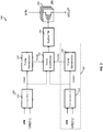
- FIG. 4 shows a single branch ILDO regulator 400 additionally comprising a timer check circuit 410.
- the timer check circuit 410 may comprise a time comparison circuit and a running timer.
- the running timer may be separate from the timer check circuit 410 and the timer check circuit 410 may receive a timing signal from the running timer.
- the comparator 210 detects an event based on the relative values of the feedback voltage VFB and the reference voltage VREF1
- the comparator 210 may send a signal indicative of the event to the timer check circuit 410 and to at least one of the pulse generator 220 and the loop controller 230.
- the timer check circuit 410 may compare the value of a running timer at the time the event from the comparator 210 is received to a threshold time T1.
- the running timer may be any suitable time keeping circuit, such as an oscillator, a clock input, or a counter.
- the threshold time may be a preset time to regulate the action taken by the loop controller 230.
- the timer check circuit 410 may also or alternatively receive the feedback voltage VFB from the comparator 210 or directly from the input to the ILDO regulator 400.
- the timer check circuit may be used to prevent the output voltage VOUT from remaining at a single level for longer than a determined period of time. For example, it may be acceptable for the output voltage to be slightly above or slightly below the desired output voltage for a short period of time, but undesirable for the output voltage to remain at that level.
- the timer check circuit 410 may trigger the loop controller 230 to correspondingly adjust the number of active switches in the switch circuit 250, even though the comparator has not caused an event.
- the time based control may allow for finer control of the output voltage VOUT in the system by using the voltage level based comparison to make changes to the output voltage and then readjusting the voltage level over time based on the timer control.
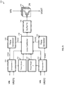
- FIG. 5 shows a double branch ILDO regulator 500, with each branch having a timer check circuit.
- the comparator 310 detects an event based on the relative values of the feedback voltage VFB and the reference voltage VREF2, the comparator may send a signal indicative of the event to the timer check circuit 510 and to at least one of the pulse generator 320 and the loop controller 230.
- the timer check circuit 510 may compare the value of a running timer at the time the event from the comparator 310 is received to a threshold time T2.
- the running timer may be any suitable time keeping mechanism, such as an oscillator, a clock input, or a counter.
- the threshold time may be a preset time to regulate the action taken by the loop controller 230, as described above.
- timer check circuit 510 may also or alternatively receive the feedback voltage VFB from the comparator 310 or directly from the input to the ILDO regulator 500. However, with multiple timer check circuits intervals may be set to regulate the action taken by the loop controller 230. For example, if T1 is less than T2, then in the case that the running timer reaches T1 with VOUT at an undesirable level, the loop controller 230 may set the number of active switches in a first configuration. If the running timer reaches a time between T1 and T2 with VOUT at an undesirable level, the loop controller 230 may set the number of active switches in a second configuration. While two separate timer check circuits 410 and 510 are shown in FIG.
- the two timer check circuits could be implemented as a single time with multiple inputs and thresholds. Additionally, it should be appreciated that while two branches are shown in FIG. 5 , any number of branches and timer check circuits may be used to provide finer control of the output voltage VOUT.
- the load circuit at the output of the ILDO regulator may comprise a mesh circuit.
- the providing the output of the ILDO regulator to one end of the mesh circuit may cause an uneven power, voltage, or current distribution across the load circuit.
- Described herein is a system with multiple ILDO regulators to provide power, voltage, or current at multiple points across the load circuit, wherein the ILDO regulators can communicate to maintain the stability of the system or otherwise improve control of the system.
- FIG. 6 shows a system 600 comprising a first ILDO regulator 620 and a second ILDO regulator 630 coupled across a load circuit 610.
- the load circuit 610 is equivalent to a resistive mesh
- the mesh may cause the voltage from the ILDO regulator to be unevenly dissipated across the load circuit 610, resulting in inefficient operation and high power loss.
- the system 600 uses a first ILDO regulator 620 on a first side of the load circuit 610 and a second ILDO regulator 630 on a second side of the load circuit 610.
- the voltage dissipation across the mesh may be reduced, and a more even power consumption may be achieved.
- the output voltages may dampen each other if they are not adjusted in a synchronous manner.
- FIG. 7 shows a system 700 with the first and second ILDOs 620 and 630 coupled across the load circuit 610.
- the load circuit 610 comprises N (unrelated to the number of switches in the ILDO switching circuit) sub-circuits arranged in a mesh network, with N being a positive integer greater than or equal to one.
- N being a positive integer greater than or equal to one.
- Each of the sub-circuits 710, 720, and 730 may act as a sub-circuit within the load circuit 610 coupled to the first and second ILDOs 620 and 630, but the resistances between each of the sub-circuits 710, 720, and 730 may cause uneven power to be dissipated across them if the first ILDO regulator 620 and the second ILDO regulator 630 operate independently.
- the first ILDO regulator 620 and the second ILDO regulator 630 may exchange control signals over a communication channel.
- the loop controller of the first ILDO regulator 620 may receive signals from the comparator, pulse generator, and/or the timer check circuit of the second ILDO regulator 630.
- the second ILDO regulator 630 detects an event on the second side of the load circuit 610 that does not occur on the first side of the load circuit 610, the first ILDO regulator 620 may be notified and the loop controller of the first ILDO regulator 620 may change the number of active switches to adjust the output voltage of the first ILDO regulator 620 and prevent a damping effect from occurring through uneven voltage applied to the load circuit 610.
- both ILDOs 620 and 630 may communicate event information to each other based on their timer check circuit, pulse generator, and/or comparators signals to maintain synchronized voltage output to the load circuit 610. While two ILDOs are shown in FIGS. 6 and 7 , it should be appreciated that any number of ILDOs may be applied to the load circuit and synchronized.
Landscapes
- Engineering & Computer Science (AREA)
- Physics & Mathematics (AREA)
- Electromagnetism (AREA)
- General Physics & Mathematics (AREA)
- Radar, Positioning & Navigation (AREA)
- Automation & Control Theory (AREA)
- Power Engineering (AREA)
- Continuous-Control Power Sources That Use Transistors (AREA)
Claims (11)
- Régulateur à faible chute qui produit une sortie, comprenant :un circuit de comparaison (210), configuré pour comparer un signal représentatif de la sortie et un signal de référence pour produire un résultat de comparaison ;un contrôleur de boucle (230), couplé au circuit de comparaison (210), configuré pour générer un signal de commande de circuit de sortie sur la base au moins en partie du résultat de comparaison ;un circuit de sortie (250), comprenant deux étages de sortie ou plus, configuré pour ajuster un certain nombre d'étages de sortie actifs des deux étages de sortie ou plus sur la base du signal de commande du circuit de sortie ; caractérisé en ce qu'il comprend :un circuit de contrôle de minuterie (410), configuré pour comparer un temps de fonctionnement d'un niveau du signal représentatif de la sortie à un premier temps de référence pour produire un signal de contrôle de temps pour ajuster le nombre d'étages de sortie actifs,dans lequel le temps de fonctionnement commence lorsque le circuit de sortie ajuste le nombre d'étages de sortie actifs, ou le temps de fonctionnement commence lorsqu'un résultat de comparaison précédent a changé d'état.
- Régulateur à faible chute selon la revendication 1, dans lequel le circuit de comparaison (210) est couplé au contrôleur de boucle (230) par le biais d'un générateur d'impulsions (220), le générateur d'impulsions (220) étant configuré pour générer une impulsion en réponse à un changement dans le résultat de comparaison.
- Régulateur de faible chute selon la revendication 2, dans lequel le contrôleur de boucle (230) est configuré pour générer le signal de commande de circuit de sortie sur la base de l'impulsion.
- Régulateur à faible chute selon la revendication 1, comprenant en outre deux amplificateurs tampons ou plus (240), couplés entre le contrôleur de boucle et le circuit de sortie.
- Régulateur à faible chute selon la revendication 2, dans lequel le générateur d'impulsions (220) est configuré pour générer un premier type d'impulsion si la sortie est supérieure au signal de référence et un second type d'impulsion si la sortie est inférieure au signal de référence.
- Régulateur à faible chute selon la revendication 1, dans lequel le contrôleur de boucle (230) est configuré pour augmenter un nombre d'étages de sortie activés des deux étages de sortie ou plus lorsque la sortie est inférieure au signal de référence.
- Régulateur à faible chute selon la revendication 1, dans lequel le contrôleur de boucle (230) est configuré pour diminuer un nombre d'étages de sortie activés des deux étages de sortie ou plus (240) lorsque la sortie est supérieure au signal de référence.
- Régulateur à faible chute selon la revendication 1, dans lequel le contrôleur de boucle (230) est en outre configuré pour générer le signal de commande de circuit de sortie sur la base du signal de contrôle de temps.
- Régulateur à faible chute selon la revendication 1, dans lequel le signal de contrôle de temps est généré lorsque le temps de fonctionnement dépasse le premier temps de référence.
- Régulateur à faible chute selon la revendication 1, comprenant en outre :un deuxième circuit de comparaison (310), configuré pour comparer un signal représentatif de la sortie et un deuxième signal de référence pour produire un deuxième résultat de comparaison,dans lequel le contrôleur de boucle (230) est en outre couplé au deuxième circuit de comparaison et est configuré pour générer le signal de commande de circuit de sortie sur la base au moins en partie du résultat de comparaison et du deuxième résultat de comparaison.
- Régulateur à faible chute selon la revendication 10, comprenant en outre :
un deuxième générateur d'impulsions (320), couplé entre le deuxième circuit de comparaison et le générateur d'impulsions, configuré pour générer une deuxième impulsion en réponse à un changement dans le deuxième résultat de comparaison.
Applications Claiming Priority (3)
| Application Number | Priority Date | Filing Date | Title |
|---|---|---|---|
| US201762468425P | 2017-03-08 | 2017-03-08 | |
| US201762468427P | 2017-03-08 | 2017-03-08 | |
| US15/907,225 US10326361B2 (en) | 2017-03-08 | 2018-02-27 | Asynchronous low dropout regulator |
Publications (2)
| Publication Number | Publication Date |
|---|---|
| EP3373103A1 EP3373103A1 (fr) | 2018-09-12 |
| EP3373103B1 true EP3373103B1 (fr) | 2021-07-14 |
Family
ID=61598890
Family Applications (1)
| Application Number | Title | Priority Date | Filing Date |
|---|---|---|---|
| EP18160329.1A Active EP3373103B1 (fr) | 2017-03-08 | 2018-03-06 | Régulateur asynchrone à faible chute de tension |
Country Status (2)
| Country | Link |
|---|---|
| US (1) | US10326361B2 (fr) |
| EP (1) | EP3373103B1 (fr) |
Families Citing this family (1)
| Publication number | Priority date | Publication date | Assignee | Title |
|---|---|---|---|---|
| US11640834B2 (en) * | 2020-10-24 | 2023-05-02 | Mediatek Singapore Pte. Ltd. | Voltage droop reduction with a secondary power supply |
Family Cites Families (8)
| Publication number | Priority date | Publication date | Assignee | Title |
|---|---|---|---|---|
| US7676239B1 (en) * | 2005-02-24 | 2010-03-09 | National Semiconductor Corporation | System and method for providing a power controller with flat amplitude and phase response |
| US7400123B1 (en) | 2006-04-11 | 2008-07-15 | Xilinx, Inc. | Voltage regulator with variable drive strength for improved phase margin in integrated circuits |
| US8098505B1 (en) * | 2009-07-20 | 2012-01-17 | Fairchild Semiconductor Corporation | Phase management for interleaved power factor correction |
| JP5635935B2 (ja) * | 2011-03-31 | 2014-12-03 | ルネサスエレクトロニクス株式会社 | 定電流生成回路、これを含むマイクロプロセッサ及び半導体装置 |
| US8912775B2 (en) * | 2011-04-12 | 2014-12-16 | Infineon Technologies Ag | Power factor correction circuit having multiple switched-mode converter circuits |
| US9484917B2 (en) | 2012-12-18 | 2016-11-01 | Intel Corporation | Digital clamp for state retention |
| US10698432B2 (en) * | 2013-03-13 | 2020-06-30 | Intel Corporation | Dual loop digital low drop regulator and current sharing control apparatus for distributable voltage regulators |
| CN205792228U (zh) * | 2015-03-17 | 2016-12-07 | 意法半导体股份有限公司 | 用于控制开关调节器的控制设备和电气装置 |
-
2018
- 2018-02-27 US US15/907,225 patent/US10326361B2/en active Active
- 2018-03-06 EP EP18160329.1A patent/EP3373103B1/fr active Active
Non-Patent Citations (1)
| Title |
|---|
| None * |
Also Published As
| Publication number | Publication date |
|---|---|
| US10326361B2 (en) | 2019-06-18 |
| US20180262105A1 (en) | 2018-09-13 |
| EP3373103A1 (fr) | 2018-09-12 |
Similar Documents
| Publication | Publication Date | Title |
|---|---|---|
| CN110196611B (zh) | 一种低压差稳压器及其系统 | |
| US8305053B2 (en) | System and method for controlling a power switch in a power supply system | |
| JP5427193B2 (ja) | スイッチングレギュレータ | |
| US9515556B2 (en) | Current pulse count control in a voltage regulator | |
| JP4303731B2 (ja) | デュアルモード電圧調整器 | |
| KR102145165B1 (ko) | 스위칭 레귤레이터 및 전자 기기 | |
| US9099927B2 (en) | Multi-voltage power supply and electronic apparatus including the same | |
| US8368475B2 (en) | Oscillator circuit | |
| US9019728B2 (en) | Power converter output voltage clamp and supply terminal | |
| EP2289143B1 (fr) | Correction d impédance | |
| TWI662392B (zh) | 降低低電流穩壓器輸出端的負脈衝訊號的電路及其方法 | |
| KR101803538B1 (ko) | 전력 공급 장치 및 그 구동 방법 | |
| CN112787506B (zh) | 带有分段线性负载线的电压调制器 | |
| US9164520B2 (en) | Synchronous rectification type power circuit and method of adjusting the same | |
| WO2016140719A2 (fr) | Topologie de régulateur de tension à mode sélectionnable | |
| US20120043951A1 (en) | Switching Regulator and Constant On-time Module | |
| US9069366B2 (en) | Switching regulator | |
| US11658673B2 (en) | Driver circuitry | |
| KR20140018790A (ko) | 케이블 보상 회로 | |
| CN101411048A (zh) | 开关模式电源控制系统 | |
| EP3159994B1 (fr) | Limiteur de courant bidirectionnel | |
| EP3373103B1 (fr) | Régulateur asynchrone à faible chute de tension | |
| US9166468B2 (en) | Voltage regulator circuit with soft-start function | |
| US20150214825A1 (en) | Pseudo-constant frequency control for voltage converter | |
| CN112350582B (zh) | 用于控制电源的方法和电路 |
Legal Events
| Date | Code | Title | Description |
|---|---|---|---|
| PUAI | Public reference made under article 153(3) epc to a published international application that has entered the european phase |
Free format text: ORIGINAL CODE: 0009012 |
|
| STAA | Information on the status of an ep patent application or granted ep patent |
Free format text: STATUS: THE APPLICATION HAS BEEN PUBLISHED |
|
| AK | Designated contracting states |
Kind code of ref document: A1 Designated state(s): AL AT BE BG CH CY CZ DE DK EE ES FI FR GB GR HR HU IE IS IT LI LT LU LV MC MK MT NL NO PL PT RO RS SE SI SK SM TR |
|
| AX | Request for extension of the european patent |
Extension state: BA ME |
|
| STAA | Information on the status of an ep patent application or granted ep patent |
Free format text: STATUS: REQUEST FOR EXAMINATION WAS MADE |
|
| 17P | Request for examination filed |
Effective date: 20190307 |
|
| RBV | Designated contracting states (corrected) |
Designated state(s): AL AT BE BG CH CY CZ DE DK EE ES FI FR GB GR HR HU IE IS IT LI LT LU LV MC MK MT NL NO PL PT RO RS SE SI SK SM TR |
|
| STAA | Information on the status of an ep patent application or granted ep patent |
Free format text: STATUS: EXAMINATION IS IN PROGRESS |
|
| 17Q | First examination report despatched |
Effective date: 20191106 |
|
| GRAP | Despatch of communication of intention to grant a patent |
Free format text: ORIGINAL CODE: EPIDOSNIGR1 |
|
| STAA | Information on the status of an ep patent application or granted ep patent |
Free format text: STATUS: GRANT OF PATENT IS INTENDED |
|
| INTG | Intention to grant announced |
Effective date: 20210223 |
|
| GRAS | Grant fee paid |
Free format text: ORIGINAL CODE: EPIDOSNIGR3 |
|
| GRAA | (expected) grant |
Free format text: ORIGINAL CODE: 0009210 |
|
| STAA | Information on the status of an ep patent application or granted ep patent |
Free format text: STATUS: THE PATENT HAS BEEN GRANTED |
|
| AK | Designated contracting states |
Kind code of ref document: B1 Designated state(s): AL AT BE BG CH CY CZ DE DK EE ES FI FR GB GR HR HU IE IS IT LI LT LU LV MC MK MT NL NO PL PT RO RS SE SI SK SM TR |
|
| REG | Reference to a national code |
Ref country code: GB Ref legal event code: FG4D |
|
| REG | Reference to a national code |
Ref country code: IE Ref legal event code: FG4D |
|
| REG | Reference to a national code |
Ref country code: DE Ref legal event code: R096 Ref document number: 602018019940 Country of ref document: DE |
|
| REG | Reference to a national code |
Ref country code: AT Ref legal event code: REF Ref document number: 1411167 Country of ref document: AT Kind code of ref document: T Effective date: 20210815 |
|
| REG | Reference to a national code |
Ref country code: LT Ref legal event code: MG9D |
|
| REG | Reference to a national code |
Ref country code: NL Ref legal event code: MP Effective date: 20210714 |
|
| REG | Reference to a national code |
Ref country code: AT Ref legal event code: MK05 Ref document number: 1411167 Country of ref document: AT Kind code of ref document: T Effective date: 20210714 |
|
| PG25 | Lapsed in a contracting state [announced via postgrant information from national office to epo] |
Ref country code: NL Free format text: LAPSE BECAUSE OF FAILURE TO SUBMIT A TRANSLATION OF THE DESCRIPTION OR TO PAY THE FEE WITHIN THE PRESCRIBED TIME-LIMIT Effective date: 20210714 Ref country code: NO Free format text: LAPSE BECAUSE OF FAILURE TO SUBMIT A TRANSLATION OF THE DESCRIPTION OR TO PAY THE FEE WITHIN THE PRESCRIBED TIME-LIMIT Effective date: 20211014 Ref country code: PT Free format text: LAPSE BECAUSE OF FAILURE TO SUBMIT A TRANSLATION OF THE DESCRIPTION OR TO PAY THE FEE WITHIN THE PRESCRIBED TIME-LIMIT Effective date: 20211115 Ref country code: LT Free format text: LAPSE BECAUSE OF FAILURE TO SUBMIT A TRANSLATION OF THE DESCRIPTION OR TO PAY THE FEE WITHIN THE PRESCRIBED TIME-LIMIT Effective date: 20210714 Ref country code: BG Free format text: LAPSE BECAUSE OF FAILURE TO SUBMIT A TRANSLATION OF THE DESCRIPTION OR TO PAY THE FEE WITHIN THE PRESCRIBED TIME-LIMIT Effective date: 20211014 Ref country code: AT Free format text: LAPSE BECAUSE OF FAILURE TO SUBMIT A TRANSLATION OF THE DESCRIPTION OR TO PAY THE FEE WITHIN THE PRESCRIBED TIME-LIMIT Effective date: 20210714 Ref country code: RS Free format text: LAPSE BECAUSE OF FAILURE TO SUBMIT A TRANSLATION OF THE DESCRIPTION OR TO PAY THE FEE WITHIN THE PRESCRIBED TIME-LIMIT Effective date: 20210714 Ref country code: SE Free format text: LAPSE BECAUSE OF FAILURE TO SUBMIT A TRANSLATION OF THE DESCRIPTION OR TO PAY THE FEE WITHIN THE PRESCRIBED TIME-LIMIT Effective date: 20210714 Ref country code: HR Free format text: LAPSE BECAUSE OF FAILURE TO SUBMIT A TRANSLATION OF THE DESCRIPTION OR TO PAY THE FEE WITHIN THE PRESCRIBED TIME-LIMIT Effective date: 20210714 Ref country code: FI Free format text: LAPSE BECAUSE OF FAILURE TO SUBMIT A TRANSLATION OF THE DESCRIPTION OR TO PAY THE FEE WITHIN THE PRESCRIBED TIME-LIMIT Effective date: 20210714 Ref country code: ES Free format text: LAPSE BECAUSE OF FAILURE TO SUBMIT A TRANSLATION OF THE DESCRIPTION OR TO PAY THE FEE WITHIN THE PRESCRIBED TIME-LIMIT Effective date: 20210714 |
|
| PG25 | Lapsed in a contracting state [announced via postgrant information from national office to epo] |
Ref country code: PL Free format text: LAPSE BECAUSE OF FAILURE TO SUBMIT A TRANSLATION OF THE DESCRIPTION OR TO PAY THE FEE WITHIN THE PRESCRIBED TIME-LIMIT Effective date: 20210714 Ref country code: LV Free format text: LAPSE BECAUSE OF FAILURE TO SUBMIT A TRANSLATION OF THE DESCRIPTION OR TO PAY THE FEE WITHIN THE PRESCRIBED TIME-LIMIT Effective date: 20210714 Ref country code: GR Free format text: LAPSE BECAUSE OF FAILURE TO SUBMIT A TRANSLATION OF THE DESCRIPTION OR TO PAY THE FEE WITHIN THE PRESCRIBED TIME-LIMIT Effective date: 20211015 |
|
| REG | Reference to a national code |
Ref country code: DE Ref legal event code: R097 Ref document number: 602018019940 Country of ref document: DE |
|
| PG25 | Lapsed in a contracting state [announced via postgrant information from national office to epo] |
Ref country code: DK Free format text: LAPSE BECAUSE OF FAILURE TO SUBMIT A TRANSLATION OF THE DESCRIPTION OR TO PAY THE FEE WITHIN THE PRESCRIBED TIME-LIMIT Effective date: 20210714 |
|
| PLBE | No opposition filed within time limit |
Free format text: ORIGINAL CODE: 0009261 |
|
| STAA | Information on the status of an ep patent application or granted ep patent |
Free format text: STATUS: NO OPPOSITION FILED WITHIN TIME LIMIT |
|
| PG25 | Lapsed in a contracting state [announced via postgrant information from national office to epo] |
Ref country code: SM Free format text: LAPSE BECAUSE OF FAILURE TO SUBMIT A TRANSLATION OF THE DESCRIPTION OR TO PAY THE FEE WITHIN THE PRESCRIBED TIME-LIMIT Effective date: 20210714 Ref country code: SK Free format text: LAPSE BECAUSE OF FAILURE TO SUBMIT A TRANSLATION OF THE DESCRIPTION OR TO PAY THE FEE WITHIN THE PRESCRIBED TIME-LIMIT Effective date: 20210714 Ref country code: RO Free format text: LAPSE BECAUSE OF FAILURE TO SUBMIT A TRANSLATION OF THE DESCRIPTION OR TO PAY THE FEE WITHIN THE PRESCRIBED TIME-LIMIT Effective date: 20210714 Ref country code: EE Free format text: LAPSE BECAUSE OF FAILURE TO SUBMIT A TRANSLATION OF THE DESCRIPTION OR TO PAY THE FEE WITHIN THE PRESCRIBED TIME-LIMIT Effective date: 20210714 Ref country code: CZ Free format text: LAPSE BECAUSE OF FAILURE TO SUBMIT A TRANSLATION OF THE DESCRIPTION OR TO PAY THE FEE WITHIN THE PRESCRIBED TIME-LIMIT Effective date: 20210714 Ref country code: AL Free format text: LAPSE BECAUSE OF FAILURE TO SUBMIT A TRANSLATION OF THE DESCRIPTION OR TO PAY THE FEE WITHIN THE PRESCRIBED TIME-LIMIT Effective date: 20210714 |
|
| 26N | No opposition filed |
Effective date: 20220419 |
|
| PG25 | Lapsed in a contracting state [announced via postgrant information from national office to epo] |
Ref country code: IT Free format text: LAPSE BECAUSE OF FAILURE TO SUBMIT A TRANSLATION OF THE DESCRIPTION OR TO PAY THE FEE WITHIN THE PRESCRIBED TIME-LIMIT Effective date: 20210714 |
|
| PG25 | Lapsed in a contracting state [announced via postgrant information from national office to epo] |
Ref country code: MC Free format text: LAPSE BECAUSE OF FAILURE TO SUBMIT A TRANSLATION OF THE DESCRIPTION OR TO PAY THE FEE WITHIN THE PRESCRIBED TIME-LIMIT Effective date: 20210714 |
|
| REG | Reference to a national code |
Ref country code: CH Ref legal event code: PL |
|
| REG | Reference to a national code |
Ref country code: BE Ref legal event code: MM Effective date: 20220331 |
|
| PG25 | Lapsed in a contracting state [announced via postgrant information from national office to epo] |
Ref country code: LU Free format text: LAPSE BECAUSE OF NON-PAYMENT OF DUE FEES Effective date: 20220306 Ref country code: LI Free format text: LAPSE BECAUSE OF NON-PAYMENT OF DUE FEES Effective date: 20220331 Ref country code: IE Free format text: LAPSE BECAUSE OF NON-PAYMENT OF DUE FEES Effective date: 20220306 Ref country code: CH Free format text: LAPSE BECAUSE OF NON-PAYMENT OF DUE FEES Effective date: 20220331 |
|
| PG25 | Lapsed in a contracting state [announced via postgrant information from national office to epo] |
Ref country code: BE Free format text: LAPSE BECAUSE OF NON-PAYMENT OF DUE FEES Effective date: 20220331 |
|
| P01 | Opt-out of the competence of the unified patent court (upc) registered |
Effective date: 20230607 |
|
| PG25 | Lapsed in a contracting state [announced via postgrant information from national office to epo] |
Ref country code: HU Free format text: LAPSE BECAUSE OF FAILURE TO SUBMIT A TRANSLATION OF THE DESCRIPTION OR TO PAY THE FEE WITHIN THE PRESCRIBED TIME-LIMIT; INVALID AB INITIO Effective date: 20180306 |
|
| PG25 | Lapsed in a contracting state [announced via postgrant information from national office to epo] |
Ref country code: MK Free format text: LAPSE BECAUSE OF FAILURE TO SUBMIT A TRANSLATION OF THE DESCRIPTION OR TO PAY THE FEE WITHIN THE PRESCRIBED TIME-LIMIT Effective date: 20210714 Ref country code: CY Free format text: LAPSE BECAUSE OF FAILURE TO SUBMIT A TRANSLATION OF THE DESCRIPTION OR TO PAY THE FEE WITHIN THE PRESCRIBED TIME-LIMIT Effective date: 20210714 |
|
| PG25 | Lapsed in a contracting state [announced via postgrant information from national office to epo] |
Ref country code: MT Free format text: LAPSE BECAUSE OF FAILURE TO SUBMIT A TRANSLATION OF THE DESCRIPTION OR TO PAY THE FEE WITHIN THE PRESCRIBED TIME-LIMIT Effective date: 20210714 |
|
| PG25 | Lapsed in a contracting state [announced via postgrant information from national office to epo] |
Ref country code: TR Free format text: LAPSE BECAUSE OF FAILURE TO SUBMIT A TRANSLATION OF THE DESCRIPTION OR TO PAY THE FEE WITHIN THE PRESCRIBED TIME-LIMIT Effective date: 20210714 |
|
| PGFP | Annual fee paid to national office [announced via postgrant information from national office to epo] |
Ref country code: FR Payment date: 20251231 Year of fee payment: 9 |
|
| PGFP | Annual fee paid to national office [announced via postgrant information from national office to epo] |
Ref country code: GB Payment date: 20260106 Year of fee payment: 9 |
|
| PGFP | Annual fee paid to national office [announced via postgrant information from national office to epo] |
Ref country code: DE Payment date: 20260102 Year of fee payment: 9 |