EP3373170A1 - Dispositif d'émulation de conceptions pour circuits intégrés - Google Patents
Dispositif d'émulation de conceptions pour circuits intégrés Download PDFInfo
- Publication number
- EP3373170A1 EP3373170A1 EP18168102.4A EP18168102A EP3373170A1 EP 3373170 A1 EP3373170 A1 EP 3373170A1 EP 18168102 A EP18168102 A EP 18168102A EP 3373170 A1 EP3373170 A1 EP 3373170A1
- Authority
- EP
- European Patent Office
- Prior art keywords
- bus
- programmable logic
- bus lines
- bus line
- logic circuits
- Prior art date
- Legal status (The legal status is an assumption and is not a legal conclusion. Google has not performed a legal analysis and makes no representation as to the accuracy of the status listed.)
- Withdrawn
Links
Images



Classifications
-
- G—PHYSICS
- G06—COMPUTING OR CALCULATING; COUNTING
- G06F—ELECTRIC DIGITAL DATA PROCESSING
- G06F30/00—Computer-aided design [CAD]
- G06F30/30—Circuit design
- G06F30/32—Circuit design at the digital level
- G06F30/33—Design verification, e.g. functional simulation or model checking
- G06F30/3308—Design verification, e.g. functional simulation or model checking using simulation
- G06F30/331—Design verification, e.g. functional simulation or model checking using simulation with hardware acceleration, e.g. by using field programmable gate array [FPGA] or emulation
Definitions
- the invention relates to a device for emulating integrated circuit designs according to the preamble of patent claim 1.
- a common method for verifying integrated circuit designs is their mapping with programmable hardware.
- programmable hardware is often constructed from programmable logic circuits, so-called FPGA (field programmable gate array) circuits.
- FPGA field programmable gate array
- an inherent property of the programmable logic circuits in particular the FPGAs, is exploited, namely that the signals from the logic circuit can be routed to any connection contacts of the logic circuit.
- the terminal contacts internal structures of the circuit are permanently assigned.
- the flexible nature of any contact of the terminals with internal structures of the logic circuit is exploited to produce in conjunction with the selectively interconnectable BUS lines exactly those combination options that are required for the design of the integrated circuit design.
- a plurality of channels of one BUS line are selectively electrically connectable to a plurality of channels of another BUS line, each channel of one BUS line being electrically connectable to the associated channel of the other BUS line, the individual channels being independent are connectable from each other.
- This configuration increases the flexibility.
- connection bus lines are provided for directly interconnecting the respective logic circuits.
- connection bus lines are provided for direct connection. As a result, the number of required switches is reduced and the signal propagation times are noticeably reduced due to the short direct connection paths.
- a plurality of receiving devices can be connected to one another via connecting devices, the connecting devices having switchable BUS lines. This makes it possible to provide a modular device which is realized by connecting a plurality of receiving devices, which may be constructed substantially identical.
- main connection means are provided, each connecting two receiving devices with each other, wherein the main connection means comprise BUS lines, each interconnecting BUS lines of the two receiving devices connect to each other and wherein the BUS lines of a main connection means so selectively with each other are electrically connected, that at least one channel of a BUS line with a channel of at least one other BUS line is electrically connected.
- main connecting devices two receiving devices can be connected to a receiving device pair in a simple manner.
- group connection devices which each connect two receptacle pairs consisting of two receptacle devices connected to a main connection device, and wherein one group connection device has BUS lines which are connected to the BUS lines of the respective receptacle pairs and wherein the bus lines of the group connection means are each switchable such that each channel of each bus line of the group connection means is associated with a switch and that the respective switches are independently switched on and off.
- the receiving devices, the main connecting devices and the group connecting devices comprise printed circuit boards which are respectively provided on their upper side and on their underside with a connector arrangement which consists of a plurality of connectors which are in the same position on the respective printed circuit board are arranged and wherein the leading outward BUS lines of the respective circuit board are electrically connected in the same way both with upper and with corresponding lower connectors of the respective connector assembly.
- This embodiment allows a modular design of the device according to the invention, since receiving devices, main connection devices and group connection devices can be easily arranged one above the other and plugged together for contacting.
- a preferred embodiment of this modular structure is characterized in that the circuit boards are arranged one above the other and mechanically and electrically connected to each other by means of the connector assemblies, wherein in each case two printed circuit boards of the receiving devices by means of a between these arranged printed circuit board of a main connecting means are sandwiched to a receiving device pair and wherein the receiving device pairs are connected to each other by means of the circuit boards of the group connecting means.
- a space is provided between some of the connectors of the respective connector assemblies to allow the passage of cooling air between the connectors through the PCB sandwich.
- the cooling air can be very effective in this arrangement, for example, according to the cross-flow principle, flow around the circuit boards and dissipate the heat generated there.
- Such a computer program accelerates the process of the circuit resolution and the connection of the individual logic circuits with each other and controls the individual switches directly.
- a receptacle 1 is shown having a circuit board 10, on the three slots 11a, 12a, 13a for programmable logic circuits 11, 12, 13 and one in the Fig. 1 only schematically illustrated electrical connection structure 14 are provided.
- Each of the bays 11a, 12a, 13a for the respective programmable logic circuits 11, 12, 13 is connected to two BUS lines 111, 112; 121, 122; 131, 132, wherein each of the BUS lines is connected to a plurality of (not shown) terminal contacts of the respective slot 11a, 12a, 13a.
- the provision of two BUS lines per slot is shown only by way of example; It can be provided per slot also only a bus line or more than two bus lines.
- BUS lines 111, 112; 121, 122; 131, 132 are connected to each other by BUS connection lines 141, 142, 143, and in each BUS connection line, one with reference to FIG Fig. 2 explained in detail BUS switching device 141 '; 142 '; 143 'is provided.
- the switchable bus connecting line 141 connects the second bus line 112 of the first slot 11 a with the first bus line 121 of the second slot 12 a.
- the BUS connection line 142 connects the second BUS line 122 of the second slot 12a to the first BUS line 131 of FIG third slot 13a.
- the BUS connection line 143 connects the second BUS line 132 of the third slot 13a to the first BUS line 111 of the first slot 11a.
- the bus switching device 141 'of the first bus connecting line 141 is shown schematically in an enlargement. It can be seen that the BUS switching device 141 'consists of a plurality of switches S 1 to S k , each of which switches one of the channels 1 to k of the BUS connecting line 141. The switches S 1 to S k can be switched on and off independently.
- the BUS switch assembly 141 ' may be configured to switch all channels of the BUS trunk 141 or only a portion thereof.
- the other BUS switching devices 142 ', 143' are formed in the same manner as the first BUS switching devices 141 '.
- a pairing of two receiving devices 1, 2 is shown, which are electrically connected to each other via a main connector 7A.
- the receptacles 1, 2 and the main connection means 7A are shown side by side for better understanding of the electrical connections in the plane. In practice, however, they are arranged one above the other, as will be described below.
- the receiving device 1 essentially corresponds to the receiving device 1 Fig. 1
- the circuit board 10 includes direct connection bus lines 15, 16, 17, wherein the connection bus line 15 connects a portion of the terminals of the first slot 11 a with a portion of the terminals of the second slot 12 a.
- the second connection bus line 16 connects a part of the terminals of the second slot 12a with a portion of the terminals of the third slot 13a and the third bus connection line 17 connects a portion of the terminals of the third slot 13a with a portion of the terminals of the first slot 11a.
- Signals are routed via these direct connection BUS lines, which are directly exchanged between the individual programmable logic circuits 11, 12, 13, without the need for flexible programming of the entire routing.
- the circuit board 10 of the first receiving device 1 also has opposite to in Fig. 1 only schematically illustrated circuit BUS switching devices 111 ', 112'; 121 ', 122'; 131 ', 132', each in the associated BUS lines 111, 112; 121, 122; 131, 132 on the associated slot 11 a; 12a; 13a opposite side of the respective bus connecting line 141; 142; 143 are provided.
- These BUS switching devices 111 ', 112'; 121 ', 122'; 131 ', 132' are the same as the ones in Fig. 2 illustrated BUS switching device.
- the BUS lines 111, 112, 121, 122, 131, 132 are on the one of the switching devices 111 ', 112'; 121 ', 122'; 131 ', 132' with respect to the associated slot 11a; 12a; 13a opposite side with arranged on top of the circuit board 10, in Fig. 3 shown only schematically, connectors of an upper connector assembly V O and arranged at the bottom of the circuit board 10, in Fig. 3 also shown only schematically, connectors of a lower connector assembly V U electrically connected. Each channel of a BUS line while a contact of the upper connector assembly V O and the corresponding contact of the lower connector assembly V U are assigned.
- the receiving device 2 consists in the example of Fig. 3 from a printed circuit board 20, which is shown mirror-inverted to the circuit board 10 of the receiving device 1 in this schematic circuit view, in the practical embodiment, the circuit boards 10 and 20, however, are constructed substantially identical.
- the recording device 2 also has three programmable logic circuits 21, 22, 23, which are connected via a connecting structure 24 with each other in the same manner as in the receiving device 1 is the case.
- the direct connection BUS lines 25, 26, 27 are provided analogously.
- the outgoing from the bays 21 a, 22 a, 23 a of the circuit board 20 BUS lines 211, 212, 221, 222, 231, 232 correspond to the BUS lines of Fig. 1 with a reference number lower by 100.
- the corresponding BUS connection lines are provided as in the receiving device 1 and provided with corresponding BUS switching devices.
- the receiving device 2 thus corresponds in structure to the receiving device. 1
- the main connecting device 7A arranged between the receiving devices 1 and 2 has corresponding BUS lines 711, 712; 721, 722; 731, 732, which connect via respective connectors of an upper connector assembly V O and a lower connector assembly V U, the respective BUS lines of the receiving devices 1 and 2 together.
- the first BUS line 711 connects the BUS line 111 of the receiving device 1 to the BUS line 211 of the receiving device 2.
- the second BUS line 712 connects the BUS line 112 of the receiving device 1 to the BUS line 212 of the receiving device 2
- the third BUS line 721 connects the BUS line 121 of the receiving device 1 to the BUS line 221 of the receiving device 2.
- the fourth BUS line 722 connects the BUS line 122 of the receiving device 1 to the BUS line 222 of the receiving device 2
- the fifth BUS line 731 connects the BUS line 131 of the receiving device 1 to the BUS line 231 of the receiving device 2.
- the sixth BUS line 732 connects the BUS line 132 of the receiving device 1 to the BUS line 232 of the receiving device 2 ,
- the main connection means 7A is provided with switchable BUS connection lines 741, 742, 743, the BUS connection line 741 connecting the second BUS line 712 to the fifth BUS line 731.
- the bus trunk 742 connects the first bus 711 to the fourth BUS line 722 and BUS connection line 743 connect the third BUS line 721 to the sixth BUS line 732.
- Each of the BUS connection lines 741, 742, 743 has a BUS switching device 741 ', 742', 743 ', each corresponding to the in Fig. 2 shown BUS switching device is constructed.
- the BUS switching devices in the main connector 7A allow in connection with the BUS switching devices of the receiving devices 1 and 2, any interconnection of the applied to the individual BUS channels terminal contacts of the respective bays 11a, 12a, 13a, 21a, 22a, 23a for the programmable logic circuits 11, 12, 13, 21, 22, 23 both in a ring structure and in a star structure, as well as in a mixed structure.
- the Fig. 3 further shows an expansion device 8, which is connected via connectors of a lower connector assembly V U with connectors of the upper connector assembly V O of the circuit board 10 of the receiving device 1, so that the BUS lines 111, 112, 121, 122, 131, 132 of the first receiving device 1 are connected to respective BUS lines 811, 812, 813, 814, 815, 816 of the extension device 8.
- the extender 8 may include, for example, a circuit board 80 on which electronic devices such as processors, memory or other integrated circuits are provided which cooperate with the programmable logic circuits of the integrated circuit design to be emulated.
- the receiving device 2 the connector of the upper connector assembly V O with the connectors of the lower Connector assembly V U of the circuit board 70 of the main connector 7A are electrically connected to the connectors of their lower connector assembly V U with a schematically illustrated adjacent board 90, which belong to a further expansion device 9 or to a group connection device described below can.
- the BUS lines 911, 912, 913, 914, 915, 916 of the printed circuit board 90 are electrically connected in a corresponding manner to the BUS lines 211, 212, 221, 222, 231, 232 of the second receiving device 2.
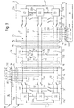
- Fig. 4 are each three receiving device pairs 1, 2; 3, 4; 5, 6 are interconnected by means of group connection devices 9A, 9B into a block of six receptacles for a total of 18 programmable logic circuits.
- the receptacle pairs 3, 4 and 5, 6 are constructed in the same way as in relation to Fig. 3 described receiving device pair 1, 3 and each consist of two receiving devices 3, 4 and 5, 6, which are connected to each other via main connecting means 7B and 7C, respectively.
- the receptacle pairs as well as the group connection devices 9A, 9B are shown below one another for a better understanding of the electrical connection in the plane. In practice, however, they are arranged flat over one another, as will be described below.
- the group connection means 9A and 9B are constructed identically and are like the extension circuit board 9 in FIG Fig. 3 connected to the adjacent receiving device 2, 4 or 4, 6, as in relation to the receiving device 2 in connection with the Fig. 3 has been described and in the Fig. 4 with respect to the receiving devices 4 and 6 is shown.
- Each of the group connection devices 9A, 9B thus has BUS lines 911, 912, 913, 914, 915 and 916 which communicate with the corresponding BUS lines of the adjacent receiving devices 2, 4 and 4, 6 in the manner already described by means of corresponding bus lines Connectors of upper and lower connector assemblies are electrically connected.
- Each of the bus lines 911, 912, 913, 914, 915, 916 is provided with a bus switching device 911 ', to 916', which is used in connection with the Fig. 2 corresponds described switching device.
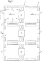
- FIG. 5 is the schematic plan view of a circuit board 10 of in Fig. 1 shown receiving device 1 shown.
- the individual channels formed as interconnects of the respective BUS lines are not shown in order not to make the figure appear confusing.
- the programmable logic circuits 11, 12, 13 and the upper connector assemblies V O are shown only schematically.
- the upper connector assembly V O comprises a plurality of connectors which are arranged in six groups V 1 , V 2 , V 3 , V 4 , V 5 , V 6 in each of six substantially square-shaped connectors P 1 , P 2 , P 3 , P 4 , P 5 , P 6 are arranged.
- Each of the connector groups V 1 , V 2 , V 3 , V 4 , V 5 , V 6 is assigned to one of the BUS lines 111, 112, 121, 122, 131, 132, and each of the BUS channels is connected to one of the contacts Connector P 1 , P 2 , P 3 , P 4 , P 5 , P 6 connected.
- the connector groups V 2 , V 3 , V 4 , V 5 and V 6 are also formed.
- Fig. 5 It can also be seen that between the longitudinal direction of the printed circuit board 10 arranged connectors P 1 and P 6, a distance L is kept free, arranged by the cooling air to the between the connectors P 3 and P 4 programmable logic circuit 11 back and forth past this flow past and on the opposite side through a corresponding opening L 'of the length L can emerge again.
- the course of the cooling air flow is schematically represented by arrows K.
- the Fig. 6 shows a side view of a stack of printed circuit boards of receiving devices 1, 2, 3, 4, 5, 6 and main connectors 7A, 7B, 7C and group connecting means 9A, 9B in the direction of arrow VI in Fig. 5 ,
- the lower connector assemblies V U are arranged in plan view congruent with the upper connector assemblies V O , so that the printed circuit boards 10, 70 A, 20, 90 A, 30, 70 B, 40, 90 B, 50, 70 C, 60 as in Fig. 6 be shown stuck together.
- Fig. 6 is also the defined by the distance L and the vertical distance between two circuit boards cooling air inlet opening or cooling air outlet opening L 'to recognize.
- both the uppermost printed circuit board 10 and the lowermost printed circuit board 60 are provided with free upper or lower plug connector arrangements V O and V U , into which further devices, for example expansion devices, can be plugged.
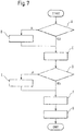
- Fig. 7 the sequence of a computer program for flexible interconnection of the connection structure of a device according to the invention is shown schematically.
- the computer program checks, in a first step A, whether there are elements in the integrated circuit design to be emulated which require a placement specification. Such elements are, for example, programmable logic circuits or expansion boards. If such elements exist, these elements are placed in a step B before all other elements with their placement default. Thereafter, in step C those elements are placed which have no placement specification. After the elements have all been placed, In step D, it is checked whether there are signals that require a fixed pin mapping, that is, a fixed assignment of terminal contacts. Such fixed pin mapping signals may be, for example, the connections from the programmable logic circuits to the extension elements. If there are such signals, they will be routed in step E with priority. Thereafter, in step F, all remaining signals are routed.
- a fixed pin mapping that is, a fixed assignment of terminal contacts.
- Such fixed pin mapping signals may be, for example, the connections from the programmable logic circuits to the extension elements. If there are such signals, they will be routed in step E with priority. Thereafter, in step F, all
- Routes are understood to mean the assignment of route paths in the entire bus connection structure.
- step G the so-called pinmappings on the programmable logic circuits are calculated, that is to say which contact of which BUS line which is present in a slot is calculated with which pin of the internal structure of the programmable logic circuit to connect.
- the device according to the invention may also assume other than the above-described embodiments.
- the device may in particular have features that represent a combination of the respective individual features of the claims.
Landscapes
- Engineering & Computer Science (AREA)
- Computer Hardware Design (AREA)
- Physics & Mathematics (AREA)
- Theoretical Computer Science (AREA)
- Evolutionary Computation (AREA)
- Geometry (AREA)
- General Engineering & Computer Science (AREA)
- General Physics & Mathematics (AREA)
- Structure Of Printed Boards (AREA)
- Design And Manufacture Of Integrated Circuits (AREA)
- Logic Circuits (AREA)
Priority Applications (1)
| Application Number | Priority Date | Filing Date | Title |
|---|---|---|---|
| EP18168102.4A EP3373170A1 (fr) | 2003-07-30 | 2003-07-30 | Dispositif d'émulation de conceptions pour circuits intégrés |
Applications Claiming Priority (2)
| Application Number | Priority Date | Filing Date | Title |
|---|---|---|---|
| EP03016640.9A EP1503307B1 (fr) | 2003-07-30 | 2003-07-30 | Appareil pour l'émulation de conceptions des circuits intégrés |
| EP18168102.4A EP3373170A1 (fr) | 2003-07-30 | 2003-07-30 | Dispositif d'émulation de conceptions pour circuits intégrés |
Related Parent Applications (2)
| Application Number | Title | Priority Date | Filing Date |
|---|---|---|---|
| EP03016640.9A Division-Into EP1503307B1 (fr) | 2003-07-30 | 2003-07-30 | Appareil pour l'émulation de conceptions des circuits intégrés |
| EP03016640.9A Division EP1503307B1 (fr) | 2003-07-30 | 2003-07-30 | Appareil pour l'émulation de conceptions des circuits intégrés |
Publications (1)
| Publication Number | Publication Date |
|---|---|
| EP3373170A1 true EP3373170A1 (fr) | 2018-09-12 |
Family
ID=33522272
Family Applications (2)
| Application Number | Title | Priority Date | Filing Date |
|---|---|---|---|
| EP18168102.4A Withdrawn EP3373170A1 (fr) | 2003-07-30 | 2003-07-30 | Dispositif d'émulation de conceptions pour circuits intégrés |
| EP03016640.9A Expired - Lifetime EP1503307B1 (fr) | 2003-07-30 | 2003-07-30 | Appareil pour l'émulation de conceptions des circuits intégrés |
Family Applications After (1)
| Application Number | Title | Priority Date | Filing Date |
|---|---|---|---|
| EP03016640.9A Expired - Lifetime EP1503307B1 (fr) | 2003-07-30 | 2003-07-30 | Appareil pour l'émulation de conceptions des circuits intégrés |
Country Status (3)
| Country | Link |
|---|---|
| US (1) | US7100130B2 (fr) |
| EP (2) | EP3373170A1 (fr) |
| CA (1) | CA2442222A1 (fr) |
Families Citing this family (6)
| Publication number | Priority date | Publication date | Assignee | Title |
|---|---|---|---|---|
| US7278120B2 (en) * | 2004-07-23 | 2007-10-02 | Synplicity, Inc. | Methods and apparatuses for transient analyses of circuits |
| US7725304B1 (en) * | 2006-05-22 | 2010-05-25 | Cadence Design Systems, Inc. | Method and apparatus for coupling data between discrete processor based emulation integrated chips |
| US7636796B2 (en) * | 2006-09-15 | 2009-12-22 | Microsoft Corporation | Smart interconnect for modular multi-component embedded devices |
| US8731899B2 (en) * | 2007-06-29 | 2014-05-20 | Seagate Technology Llc | Adapter assembly for concurrent emulation of a native channel |
| WO2016185758A1 (fr) * | 2015-05-15 | 2016-11-24 | 株式会社Nttドコモ | Équipement utilisateur et station de base |
| US10397314B2 (en) * | 2015-11-24 | 2019-08-27 | International Business Machines Corporation | Latency management and advising tool for a database management system |
Citations (2)
| Publication number | Priority date | Publication date | Assignee | Title |
|---|---|---|---|---|
| EP0651343A1 (fr) | 1988-10-05 | 1995-05-03 | Quickturn Systems Inc | Procédé pour utiliser des puces logiques de circuits prédiffusés reconfigurables électroniquement et appareil ainsi formé |
| US6263484B1 (en) * | 1997-10-01 | 2001-07-17 | Yang-Sei Yang | Prototyping system and a method of operating the same |
Family Cites Families (1)
| Publication number | Priority date | Publication date | Assignee | Title |
|---|---|---|---|---|
| US5742181A (en) * | 1996-06-04 | 1998-04-21 | Hewlett-Packard Co. | FPGA with hierarchical interconnect structure and hyperlinks |
-
2003
- 2003-07-30 EP EP18168102.4A patent/EP3373170A1/fr not_active Withdrawn
- 2003-07-30 EP EP03016640.9A patent/EP1503307B1/fr not_active Expired - Lifetime
- 2003-08-26 US US10/649,230 patent/US7100130B2/en not_active Expired - Lifetime
- 2003-09-23 CA CA002442222A patent/CA2442222A1/fr not_active Abandoned
Patent Citations (2)
| Publication number | Priority date | Publication date | Assignee | Title |
|---|---|---|---|---|
| EP0651343A1 (fr) | 1988-10-05 | 1995-05-03 | Quickturn Systems Inc | Procédé pour utiliser des puces logiques de circuits prédiffusés reconfigurables électroniquement et appareil ainsi formé |
| US6263484B1 (en) * | 1997-10-01 | 2001-07-17 | Yang-Sei Yang | Prototyping system and a method of operating the same |
Non-Patent Citations (3)
| Title |
|---|
| CARRERA J M ET AL: "Architecture of a FPGA-based coprocessor: the PAR-1", FPGAS FOR CUSTOM COMPUTING MACHINES, 1995. PROCEEDINGS. IEEE SYMPOSIUM ON NAPA VALLEY, CA, USA 19-21 APRIL 1995, LOS ALAMITOS, CA, USA,IEEE COMPUT. SOC, US, 19 April 1995 (1995-04-19), pages 20 - 29, XP010151150, ISBN: 0-8186-7086-X * |
| HAUCK S: "THE ROLES OF FPGA'S IN REPROGRAMMABLE SYSTEMS", PROCEEDINGS OF THE IEEE, IEEE. NEW YORK, US, vol. 86, no. 4, 1 April 1998 (1998-04-01), pages 613 - 638, XP000778371, ISSN: 0018-9219 * |
| KHALID M: "Routing Architecture and Layout Synthesis for Multi-FPGA Systems", 1999 - 1999, University of Toronto, Dept. of ECE, pages 1 - 132, XP002260806, Retrieved from the Internet <URL:http://www.eecg.toronto.edu/~jayar/pubs/theses/Khalid/MohammedKhalid.pdf> [retrieved on 20031107] * |
Also Published As
| Publication number | Publication date |
|---|---|
| EP1503307B1 (fr) | 2019-04-03 |
| US7100130B2 (en) | 2006-08-29 |
| EP1503307A1 (fr) | 2005-02-02 |
| US20050028127A1 (en) | 2005-02-03 |
| CA2442222A1 (fr) | 2005-01-30 |
Similar Documents
| Publication | Publication Date | Title |
|---|---|---|
| EP0712267B1 (fr) | Installation de commande modulaire avec connexion sur bus secteur intégré | |
| EP3275051B1 (fr) | Système de bus modulaire | |
| DE60034751T2 (de) | Schalttopologie mit kreuzzwischenebene | |
| DE69033582T4 (de) | Je nach Anwendungsgebiet programmierbare gedruckte Schaltungsplatte und CAD-Verfahren dazu | |
| DE602004010162T2 (de) | Effiziente schaltarchitektur mit verringerten stub-längen | |
| DE4106601C2 (de) | Verbindungssystem für Kabel in eigensicheren Industrie-Schalttafeln | |
| DE102005060081B4 (de) | Elektronisches Bauteil mit zumindest einer Leiterplatte und mit einer Mehrzahl gleichartiger Halbleiterbausteine und Verfahren | |
| DE10351392B4 (de) | Verbindungskasten | |
| EP1503307B1 (fr) | Appareil pour l'émulation de conceptions des circuits intégrés | |
| EP0740082A1 (fr) | Dispositif électrique modulaire pour un assemblage de bloc de vannes | |
| DE10148470A1 (de) | Vorrichtung und Verfahren zum elektrischen und mechanischen Verbinden von Komponenten eines Automatisierungssystems | |
| DE102021117571A1 (de) | Kraftfahrzeugsteuergerät | |
| EP3660603B1 (fr) | Module fonctionnel pouvant être disposé en rang, adapté bus | |
| DE102014111031B4 (de) | Modul, Koppeleinheit und Steuerungssystem | |
| EP0240580B2 (fr) | Dispositif de couplage à trois étages | |
| DE4232267C2 (de) | Leiterplatte mit optimierter Bausteinanordnung insbesondere für Koppelfelder mit hoher Datenrate | |
| DE3249507T1 (de) | Reihen- oder schichtenweise angeordnete, senkrecht zueinander in Bezug stehende, drei dimensionale gedruckte Plattenschaltung | |
| EP0331614A1 (fr) | Adapteur pour un dispositif de test pour circuits imprimés | |
| DE29810091U1 (de) | Ventilterminal mit einer Reihe von Schaltventilen | |
| EP0940066B1 (fr) | Dispositif de codage d'unites enfichables et dispositif de connexion de lignes exterieures au moyen d'un tel dispositif de codage | |
| DE4129332A1 (de) | Bussystem fuer bestueckbare baugruppentraeger | |
| DE10047147B4 (de) | Integrierte Halbleiterschaltung, insbesondere Halbleiterspeicherschaltung und diese verwendendes Halbleiterschaltungsmodul | |
| DE3014265C2 (de) | Mehrstufiges Koppelfeld, insbesondere zur Verkopplung höherfrequenter Signalquellen und -senken | |
| DE10110587A1 (de) | Modular stapelbares Platinensystem | |
| DE19610742A1 (de) | Baugruppe mit einer Schaltungsanordnung |
Legal Events
| Date | Code | Title | Description |
|---|---|---|---|
| PUAI | Public reference made under article 153(3) epc to a published international application that has entered the european phase |
Free format text: ORIGINAL CODE: 0009012 |
|
| AC | Divisional application: reference to earlier application |
Ref document number: 1503307 Country of ref document: EP Kind code of ref document: P |
|
| AK | Designated contracting states |
Kind code of ref document: A1 Designated state(s): AT BE BG CH CY CZ DE DK EE ES FI FR GB GR HU IE IT LI LU MC NL PT RO SE SI SK TR |
|
| STAA | Information on the status of an ep patent application or granted ep patent |
Free format text: STATUS: THE APPLICATION IS DEEMED TO BE WITHDRAWN |
|
| 18D | Application deemed to be withdrawn |
Effective date: 20190313 |