EP3376261A1 - Röntgendetektor aufweisend ein konverterelement mit umverdrahtungseinheit - Google Patents
Röntgendetektor aufweisend ein konverterelement mit umverdrahtungseinheit Download PDFInfo
- Publication number
- EP3376261A1 EP3376261A1 EP17161126.2A EP17161126A EP3376261A1 EP 3376261 A1 EP3376261 A1 EP 3376261A1 EP 17161126 A EP17161126 A EP 17161126A EP 3376261 A1 EP3376261 A1 EP 3376261A1
- Authority
- EP
- European Patent Office
- Prior art keywords
- unit
- converter element
- evaluation unit
- rewiring
- ray detector
- Prior art date
- Legal status (The legal status is an assumption and is not a legal conclusion. Google has not performed a legal analysis and makes no representation as to the accuracy of the status listed.)
- Granted
Links
Images


Classifications
-
- G—PHYSICS
- G01—MEASURING; TESTING
- G01N—INVESTIGATING OR ANALYSING MATERIALS BY DETERMINING THEIR CHEMICAL OR PHYSICAL PROPERTIES
- G01N23/00—Investigating or analysing materials by the use of wave or particle radiation, e.g. X-rays or neutrons, not covered by groups G01N3/00 – G01N17/00, G01N21/00 or G01N22/00
- G01N23/02—Investigating or analysing materials by the use of wave or particle radiation, e.g. X-rays or neutrons, not covered by groups G01N3/00 – G01N17/00, G01N21/00 or G01N22/00 by transmitting the radiation through the material
- G01N23/04—Investigating or analysing materials by the use of wave or particle radiation, e.g. X-rays or neutrons, not covered by groups G01N3/00 – G01N17/00, G01N21/00 or G01N22/00 by transmitting the radiation through the material and forming images of the material
- G01N23/046—Investigating or analysing materials by the use of wave or particle radiation, e.g. X-rays or neutrons, not covered by groups G01N3/00 – G01N17/00, G01N21/00 or G01N22/00 by transmitting the radiation through the material and forming images of the material using tomography, e.g. computed tomography [CT]
-
- G—PHYSICS
- G01—MEASURING; TESTING
- G01T—MEASUREMENT OF NUCLEAR OR X-RADIATION
- G01T1/00—Measuring X-radiation, gamma radiation, corpuscular radiation, or cosmic radiation
- G01T1/16—Measuring radiation intensity
- G01T1/24—Measuring radiation intensity with semiconductor detectors
- G01T1/241—Electrode arrangements, e.g. continuous or parallel strips or the like
-
- G—PHYSICS
- G01—MEASURING; TESTING
- G01T—MEASUREMENT OF NUCLEAR OR X-RADIATION
- G01T1/00—Measuring X-radiation, gamma radiation, corpuscular radiation, or cosmic radiation
- G01T1/16—Measuring radiation intensity
- G01T1/24—Measuring radiation intensity with semiconductor detectors
- G01T1/243—Modular detectors, e.g. arrays formed from self contained units
-
- A—HUMAN NECESSITIES
- A61—MEDICAL OR VETERINARY SCIENCE; HYGIENE
- A61B—DIAGNOSIS; SURGERY; IDENTIFICATION
- A61B6/00—Apparatus or devices for radiation diagnosis; Apparatus or devices for radiation diagnosis combined with radiation therapy equipment
- A61B6/02—Arrangements for diagnosis sequentially in different planes; Stereoscopic radiation diagnosis
- A61B6/03—Computed tomography [CT]
- A61B6/032—Transmission computed tomography [CT]
- A61B6/035—Mechanical aspects of CT
-
- A—HUMAN NECESSITIES
- A61—MEDICAL OR VETERINARY SCIENCE; HYGIENE
- A61B—DIAGNOSIS; SURGERY; IDENTIFICATION
- A61B6/00—Apparatus or devices for radiation diagnosis; Apparatus or devices for radiation diagnosis combined with radiation therapy equipment
- A61B6/40—Arrangements for generating radiation specially adapted for radiation diagnosis
- A61B6/4007—Arrangements for generating radiation specially adapted for radiation diagnosis characterised by using a plurality of source units
- A61B6/4014—Arrangements for generating radiation specially adapted for radiation diagnosis characterised by using a plurality of source units arranged in multiple source-detector units
-
- A—HUMAN NECESSITIES
- A61—MEDICAL OR VETERINARY SCIENCE; HYGIENE
- A61B—DIAGNOSIS; SURGERY; IDENTIFICATION
- A61B6/00—Apparatus or devices for radiation diagnosis; Apparatus or devices for radiation diagnosis combined with radiation therapy equipment
- A61B6/42—Arrangements for detecting radiation specially adapted for radiation diagnosis
- A61B6/4208—Arrangements for detecting radiation specially adapted for radiation diagnosis characterised by using a particular type of detector
-
- G—PHYSICS
- G01—MEASURING; TESTING
- G01T—MEASUREMENT OF NUCLEAR OR X-RADIATION
- G01T1/00—Measuring X-radiation, gamma radiation, corpuscular radiation, or cosmic radiation
- G01T1/16—Measuring radiation intensity
- G01T1/24—Measuring radiation intensity with semiconductor detectors
- G01T1/247—Detector read-out circuitry
-
- G—PHYSICS
- G01—MEASURING; TESTING
- G01T—MEASUREMENT OF NUCLEAR OR X-RADIATION
- G01T1/00—Measuring X-radiation, gamma radiation, corpuscular radiation, or cosmic radiation
- G01T1/29—Measurement performed on radiation beams, e.g. position or section of the beam; Measurement of spatial distribution of radiation
- G01T1/2914—Measurement of spatial distribution of radiation
- G01T1/2921—Static instruments for imaging the distribution of radioactivity in one or two dimensions; Radio-isotope cameras
- G01T1/2928—Static instruments for imaging the distribution of radioactivity in one or two dimensions; Radio-isotope cameras using solid state detectors
-
- H—ELECTRICITY
- H10—SEMICONDUCTOR DEVICES; ELECTRIC SOLID-STATE DEVICES NOT OTHERWISE PROVIDED FOR
- H10F—INORGANIC SEMICONDUCTOR DEVICES SENSITIVE TO INFRARED RADIATION, LIGHT, ELECTROMAGNETIC RADIATION OF SHORTER WAVELENGTH OR CORPUSCULAR RADIATION
- H10F30/00—Individual radiation-sensitive semiconductor devices in which radiation controls the flow of current through the devices, e.g. photodetectors
- H10F30/20—Individual radiation-sensitive semiconductor devices in which radiation controls the flow of current through the devices, e.g. photodetectors the devices having potential barriers, e.g. phototransistors
- H10F30/29—Individual radiation-sensitive semiconductor devices in which radiation controls the flow of current through the devices, e.g. photodetectors the devices having potential barriers, e.g. phototransistors the devices being sensitive to radiation having very short wavelengths, e.g. X-rays, gamma-rays or corpuscular radiation
-
- H—ELECTRICITY
- H10—SEMICONDUCTOR DEVICES; ELECTRIC SOLID-STATE DEVICES NOT OTHERWISE PROVIDED FOR
- H10F—INORGANIC SEMICONDUCTOR DEVICES SENSITIVE TO INFRARED RADIATION, LIGHT, ELECTROMAGNETIC RADIATION OF SHORTER WAVELENGTH OR CORPUSCULAR RADIATION
- H10F39/00—Integrated devices, or assemblies of multiple devices, comprising at least one element covered by group H10F30/00, e.g. radiation detectors comprising photodiode arrays
- H10F39/10—Integrated devices
- H10F39/12—Image sensors
- H10F39/191—Photoconductor image sensors
- H10F39/195—X-ray, gamma-ray or corpuscular radiation imagers
-
- H—ELECTRICITY
- H10—SEMICONDUCTOR DEVICES; ELECTRIC SOLID-STATE DEVICES NOT OTHERWISE PROVIDED FOR
- H10F—INORGANIC SEMICONDUCTOR DEVICES SENSITIVE TO INFRARED RADIATION, LIGHT, ELECTROMAGNETIC RADIATION OF SHORTER WAVELENGTH OR CORPUSCULAR RADIATION
- H10F77/00—Constructional details of devices covered by this subclass
- H10F77/20—Electrodes
-
- H—ELECTRICITY
- H10—SEMICONDUCTOR DEVICES; ELECTRIC SOLID-STATE DEVICES NOT OTHERWISE PROVIDED FOR
- H10W—GENERIC PACKAGES, INTERCONNECTIONS, CONNECTORS OR OTHER CONSTRUCTIONAL DETAILS OF DEVICES COVERED BY CLASS H10
- H10W72/00—Interconnections or connectors in packages
- H10W72/20—Bump connectors, e.g. solder bumps or copper pillars; Dummy bumps; Thermal bumps
-
- H—ELECTRICITY
- H10—SEMICONDUCTOR DEVICES; ELECTRIC SOLID-STATE DEVICES NOT OTHERWISE PROVIDED FOR
- H10W—GENERIC PACKAGES, INTERCONNECTIONS, CONNECTORS OR OTHER CONSTRUCTIONAL DETAILS OF DEVICES COVERED BY CLASS H10
- H10W90/00—Package configurations
- H10W90/701—Package configurations characterised by the relative positions of pads or connectors relative to package parts
- H10W90/721—Package configurations characterised by the relative positions of pads or connectors relative to package parts of bump connectors
Definitions
- the invention relates to an X-ray detector comprising a converter element with a rewiring unit formed on a surface of the converter element facing one of the evaluation unit, as well as a medical device and a production method therefor.
- X-ray imaging for example in computed tomography, angiography or radiography, counting direct-conversion X-ray detectors or integrating indirect-conversion X-ray detectors can be used.
- the X-ray radiation or the photons can be converted into electrical pulses by means of a suitable converter material in directly converting X-ray detectors.
- a suitable converter material for example, CdTe, CZT, CdZnTeSe, CdTeSe, CdMnTe, InP, TlBr2, HgI2, GaAs or others can be used.
- the electrical pulses for example voltage pulses, are evaluated by evaluation electronics, for example an integrated circuit (Application Specific Integrated Circuit, ASIC), in an evaluation unit.
- ASIC Application Specific Integrated Circuit
- the magnitude of the electrical pulse is usually proportional to the energy of the absorbed X-ray photon.
- spectral information can be extracted by comparing the magnitude of the electrical pulse with a threshold.
- the evaluation unit can be connected to a carrier unit, for example a carrier ceramic, so that increased mechanical stability can be achieved and rewiring of the signal connections to subsequent signal processing units is provided can.
- a scattered radiation grating may be formed on the side of the converter element facing the radiation source.
- a direct-conversion X-ray detector which has at least one electrode applied to a semiconductor.
- the at least one electrode and the semiconductor are electrically conductively connected, wherein the at least one electrode is transparent and electrically conductive.
- a detector module for X-ray computed tomography wherein on a front side of a printed circuit board, a sensor array having a plurality of sensor elements is mounted.
- a sensor array having a plurality of sensor elements is mounted.
- at least one heating element for heating the sensor array and an arranged in the vicinity of the heating control electronics for controlling the heating element is provided at the rear side facing away from the sensor array.
- the invention is based on the problem that the evaluation unit and the converter element have a substantially equal areal extent to obtain a mechanically stable stack structure, and thus the cost is high, since the costs of the evaluation depend on the areal extent of the evaluation.
- the object is achieved by an X-ray detector according to claim 1, a medical device according to claim 10 and a method according to claim 12.
- the invention relates to a counting X-ray detector comprising a stack arrangement with a converter element, a rewiring unit and an evaluation unit.
- the converter element has a first electrode on a surface remote from the evaluation unit and a pixelated second electrode with a plurality of electrode elements on a surface facing the evaluation unit.
- the evaluation unit has pixel electrodes.
- the rewiring unit is formed on a surface of the converter element facing the evaluation unit, wherein first contacts of electrically conductive connections between the electrode elements and the pixel electrodes are provided on a surface of the rewiring unit facing the converter element and have a first areal distribution, and second contacts of those between the two Electrode elements and the pixel electrodes are provided electrically conductive connections on one of the evaluation unit facing surface of the rewiring unit and have a smaller compared to the first area distribution second area distribution.
- a planar extension of the evaluation unit is smaller than a flat extension of the converter element.
- The, in particular direct-converting, areal converter element and the planar evaluation unit are arranged one above the other in a stack arrangement, wherein the areal expansions run parallel to one another.
- the converter element and the evaluation unit can be electrically conductively connected via electrically conductive connections in the rewiring unit and solder connections or adhesive connections, in particular the electrode elements and the pixel electrodes can be electrically conductively connected.
- the electrically conductive connections between the electrode elements and the pixel electrodes may be substantially the same length or different lengths.
- the solder connections or the adhesive connections can in particular be formed between the rewiring unit and the evaluation unit.
- the solder connections or the adhesive connections can be between be formed of the second contacts and the pixel electrodes.
- the rewiring unit can be produced directly on the surface of the converter element facing the evaluation unit by means of a lithographic method.
- the rewiring unit may be formed directly on the converter element.
- the rewiring unit may be inseparably connected to the converter element.
- the terminal area is reduced from the electrode elements to the pixel electrodes.
- the areal extent of the evaluation unit can be smaller by a factor of 4, for example, than a planar extent of the converter element. For example, the factor may assume values in the range of 1.5 to 5.
- the first electrode may be formed as a planar or structured electrode.
- the pixelated second electrode has a plurality of electrode elements. The number of electrode elements determines the number of pixels or detector elements.
- a high voltage may be applied between the first electrode and the pixelated second electrode having a plurality of electrode elements, so that the electron-hole pairs triggered by the incident X-ray radiation are separated and electrical pulses are registered in the evaluation unit.
- the high voltage can be for example -1000V.
- the rewiring unit and the evaluation unit connected to the rewiring unit can in particular be arranged centrally on the converter element.
- the evaluation unit facing surface of the converter element is located in operation on the surface facing away from the radiation source of the converter element.
- the evaluation unit facing away from the surface of the converter element is located in operation on the radiation source facing surface of the converter element.
- Each electrode element may be associated with a pixel electrode.
- Each electrode element can in particular be electrically conductively connected to a pixel electrode by means of electrically conductive connections of the rewiring unit.
- the first contacts of the electrically conductive connections are in electrically conductive connection with the electrode elements.
- the second contacts of the electrically conductive connections are in electrically conductive connection with pixel electrodes.
- the first planar distribution or / and the second planar distribution can also be referred to as density of the first contacts or second contacts.
- the distances between adjacent first contacts may be greater than the distances between adjacent second contacts.
- the first areal distribution of the first contacts can substantially correspond to the areal distribution of the electrode elements.
- the second area distribution of the second contacts may substantially correspond to the areal distribution of the pixel electrodes.
- the first contacts may, in particular in each case, have substantially the same planar extensions as the electrode elements.
- the second contacts can have, in particular in each case, essentially the same areal extent as the pixel electrodes.
- Each pixel electrode may have a smaller areal extent compared to an electrode element.
- the pixel electrode may be smaller by a factor of 4 compared to an electrode element. The factor may be in the range of 1.5 to 5, for example.
- the cost of production can be reduced.
- the area of the evaluation unit can be reduced.
- the rewiring unit directly on the converter element can advantageously replace a so-called interposer for rewiring inexpensively.
- the rewiring unit is advantageously mechanically stable, in particular also under temperature changes during operation.
- the integration density of the X-ray detector can be increased.
- smaller subunits of the X-ray detector can be realized.
- the structural complexity of the X-ray detector can be reduced. Due to the decoupling of the pixel structures in the converter element and the evaluation unit, a greater flexibility in the relative positioning of the evaluation unit in relation to the converter element can advantageously be made possible.
- the gap dimensions between adjacent evaluation units or evaluation unit and converter element can be chosen relatively freely.
- the electrically conductive connections of the rewiring unit comprise at least a first section perpendicular to a surface normal of the evaluation unit facing surface of the converter element and at least a second section parallel to the surface normal of the evaluation unit facing surface of the converter element.
- the first areal distribution can be reduced to a smaller second areal distribution.
- the electrode elements can be connected to the pixel electrodes of the smaller evaluation unit compared to the converter element.
- the rewiring unit comprises an electrically insulating material.
- the rewiring unit has at least one electrically insulating layer.
- the electrically insulating layer can electrically insulate the electrically conductive connections with respect to the converter element, the evaluation unit and adjacent further electrically conductive connections.
- the electrical signals are not disturbed.
- the first section is at least partially perpendicular to the surface normal of the evaluation unit facing surface of the converter element surrounded by the at least one electrically insulating layer and / or the second portion parallel to the surface normal of the evaluation unit facing surface of the converter element at least partially surrounded by the at least one electrically insulating layer and / or another electrically insulating layer.
- the first portion and / or the second portion are completely surrounded by the insulating layer and / or a further insulating layer.
- a rewiring can be formed by means of the electrically conductive connections within the insulating layer or the insulating layers.
- the rewiring unit has a metallic intermediate layer.
- the electric field lines in the converter element are advantageously uninfluenced by the rewiring unit or the electrically conductive connections of the rewiring unit.
- the line resistance can advantageously be very low.
- the possible metallic intermediate layer can serve as a shield in such a way that the electric field lines in the converter element or the electrical signals through the rewiring unit are substantially unaffected.
- the shield may be formed by a plurality of metallic intermediate layers in the rewiring unit.
- the rewiring unit has a flexible intermediate layer.
- the possible flexible intermediate layer can minimize mechanical stresses in the X-ray detector, so that signal instabilities are advantageously reduced or avoided.
- the flexible intermediate layer can be produced as a partial step in a lithographic process.
- the flexible intermediate layer may comprise a suitable, flexible or soft, in particular electrically insulating, material. The flexible material can compensate for mechanical tension.
- the X-ray detector further comprises a heating element for adjusting a temperature of the converter element.
- the temperature of the X-ray detector, in particular of the converter element can be advantageously stabilized or regulated by means of the possible heating element.
- the heating element can be arranged, for example, on the carrier unit.
- the heating element may be arranged, for example, on the first electrode.
- the heating element may be, for example, a Peltier element or an electrically operable heating loop.
- the first electrode is transparent to visible light, infrared light or ultraviolet light.
- the first electrode may be transparent to allow additional illumination of the converter element with infrared, ultraviolet or visible light.
- the X-ray detector further comprises a lighting unit for illuminating the converter element with visible light, infrared light or ultraviolet light.
- a lighting unit for illuminating the converter element with visible light, infrared light or ultraviolet light.
- the first visible light, infrared or ultraviolet light electrode is made opaque.
- the first electrode may be non-transparent, especially for infrared, ultraviolet or visible light.
- the X-ray detector further has a carrier unit connected to the evaluation unit.
- the carrier unit can advantageously mechanically stabilize the X-ray detector.
- the carrier unit may be mechanically and in particular also electrically conductively connected to the evaluation unit, for example by means of a solder connection or an adhesive connection, so that the signals of the evaluation unit can be led away from the X-ray detector via the carrier unit.
- the carrier unit is at least mechanically connected to the rewiring unit.
- the carrier unit may be at least mechanically connected to the converter unit, for example by means of a solder connection or an adhesive connection.
- the carrier unit can advantageously mechanically stabilize the X-ray detector.
- the invention further relates to a medical device comprising an X-ray detector according to the invention.
- a medical device comprising an X-ray detector according to the invention.
- the advantages of the X-ray detector according to the invention can be transferred to the medical device according to the invention.
- the cost of production can be reduced.
- the medical device is a computed tomography system.
- the mechanical stability can meet the requirements of a rotating X-ray detector.
- the invention further relates to a method for producing an X-ray detector comprising the steps of providing, applying and connecting.
- a converter element is provided having a first electrode on a first surface and a pixelated second electrode with a plurality of electrode elements on a second surface and an evaluation unit with pixel electrodes.
- a rewiring unit is applied to the second surface of the converter element, wherein first contacts of electrically conductive connections between the electrode elements and the pixel electrodes are provided and have a first areal distribution on a surface of the rewiring unit facing the converter element and second contacts of those between the electrode elements and the pixel electrodes electrically conductive connections on a the evaluation unit facing surface of the rewiring unit are provided and have a smaller compared to the first distribution second area distribution.
- the rewiring unit is connected to the evaluation unit by means of electrically conductive connections between the second contacts and the pixel electrodes.
- the bonding may include the use of an electrically conductive adhesive or a solder joint.
- the possible soldering process for connecting the converter element by means of solder connection to the evaluation unit advantageously takes place on the rewiring unit, in particular comprising an insulating layer.
- the diffusion of solder material into the converter element can be avoided.
- a so-called under-bump metallization can be dispensed with or simplified.
- the rewiring unit can reduce stresses due to the possible introduction of an underfill.
- signal instabilities, so-called drift spots can be avoided.
- the applying step comprises a lithographic process.
- the electrically conductive compounds and the insulating layer can be used up in a lithographic process.
- the applying step comprises applying at least one insulating layer.
- the application can be carried out as follows: An insulating layer, for example by means of a mask, can be applied to the provided converter element, the electrode elements preferably being left free. On the released electrode elements, an electrically conductive material can be applied, so that a first contact is formed. On the insulating layer, a first compound comprising an electrically conductive material be applied. Subsequently, a further insulating layer can be applied by means of a further mask, wherein at least one point for contacting the second compound is left free. It is formed by means of an electrically conductive material from the released point, the second connection. It is formed by means of an electrical material from the second compound, the third connection, the end of which is the second contact.
- an additional insulating layer may be applied, which touches the evaluation unit at least partially after the connection.
- the applying step comprises the application of a metallic intermediate layer or / and a flexible intermediate layer.
- the metallic intermediate layer or / and the flexible intermediate layer can in particular be applied to an insulating intermediate layer.
- the metallic intermediate layer may in particular be electrically insulated from the electrically conductive connection.
- the electrically conductive connections can run through the metallic intermediate layer or the flexible intermediate layer, so that a continuous electrically conductive connection is formed.
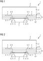
- the Fig. 1 shows an exemplary embodiment of the inventive X-ray detector 1 in a first embodiment.
- the X-ray detector 1 has a stack arrangement with a converter element 3, a rewiring unit 5 and an evaluation unit 7.
- the converter element 3 has a first electrode 2 on a surface remote from the evaluation unit 7 and a pixelated second electrode with a plurality of electrode elements 4 on a surface facing the evaluation unit 7.
- the evaluation unit 7 has pixel electrodes 6.
- the rewiring unit 5 is formed on a surface of the converter element 3 facing the evaluation unit 7, wherein first contacts of connections 8, 9, 11, 13, which are electrically conductive between the electrode elements 4 and the pixel electrodes 6, are provided on a surface of the rewiring unit 5 facing the converter element 3 and a first areal distribution, and second contacts of the between the electrode elements 4 and the pixel electrodes 6 electrically conductive connections 8, 9, 11, 13 are provided on one of the evaluation unit 7 facing surface of the rewiring unit 5 and one compared to the first planar distribution have smaller second area distribution.
- An areal extent of the evaluation unit 7 is smaller than a planar extent of the converter element 3.
- the electrically conductive connections 8, 9, 11, 13 of the rewiring unit 5 comprise at least a first section 9 perpendicular to a surface normal of the evaluating unit 7 facing surface of the converter element 3 and at least a second portion 11 parallel to the surface normal of the evaluation unit 7 facing surface of the converter element 3 include.
- the rewiring unit 5 has an electrically insulating layers 15 ', 15 ", 15"'.
- the first section 9 perpendicular to the surface normal of the evaluation unit 7 facing surface of the converter element 3 is at least partially surrounded by the at least one electrically insulating layer 15 'and / or the second portion 11 parallel to the surface normal of the evaluation unit 7 facing surface of the converter element 3 is at least partially surrounded by the at least one electrically insulating layer 15 'and further electrically insulating layers 15 ", 15'".
- the Fig. 2 shows an exemplary embodiment of the inventive X-ray detector 1 in a second embodiment.
- the rewiring unit 5 has a metallic intermediate layer 17.
- the Fig. 3 shows an exemplary embodiment of the inventive X-ray detector 1 in a third embodiment.
- the rewiring unit 5 has a flexible intermediate layer 19.
- the Fig. 4 shows an exemplary embodiment of the inventive X-ray detector 1 in a fourth embodiment.
- the X-ray detector 1 further has a carrier unit 23 connected to the evaluation unit 7.
- the X-ray detector 1 further has a heating element 21 for setting a temperature of the converter element 3.
- the heating element 21 is comprised by the carrier unit 23 or / and by the first electrode 2.
- the carrier unit 23 is at least mechanically by means of solder joints 25 with the rewiring unit 5 connected.
- the X-ray detector 1 also has a scattered radiation grating 27. Schematically, only one grid wall of the scattered beam grid 27 is shown.
- the Fig. 5 shows an exemplary embodiment of a rewiring unit 5 of the X-ray detector 1 according to the invention in a plan view.
- the areal extent of the insulating layer 15 ' is greater than the areal extent of the insulating layer 15 "
- the first connection 8, 9 runs on the surface of the insulating layer 15'
- the second connection 8, 11 connects the first connection 8, 9 of the third connection 8, 13.
- the third connection 8, 13 runs on the surface of the insulating layer 15 ".
- the pixel electrodes 6 have a smaller areal extent than the electrode elements 4.
- the Fig. 6 shows an exemplary embodiment of a rewiring unit 5 directly on the converter element 3 of the X-ray detector 1 according to the invention in a side view.
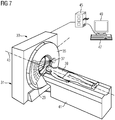
- the Fig. 7 shows an exemplary embodiment of a computed tomography system 31 according to the invention with an X-ray detector according to the invention.
- the computer tomography system 31 includes a gantry 33 with a rotor 35.
- the rotor 35 comprises an X-ray source 37 and a detector device 29 comprising at least one X-ray detector according to the invention.
- the patient 39 is mounted on the patient couch 41 and is movable along the rotation axis z 43 through the gantry 33.
- a computing unit 45 is used for controlling and calculating the sectional images.
- An input device 47 and an output device 49 are connected to the arithmetic unit 45.
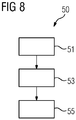
- the Fig. 8 shows an exemplary representation of the method 50 for producing an X-ray detector according to the invention comprising the steps of providing 51, the application 53 and the connection 55.
- a converter element having a first An electrode on a first surface and a pixelated second electrode provided with a plurality of electrode elements on a second surface and an evaluation unit provided with pixel electrodes.
- a rewiring unit is applied to the second surface of the converter element, wherein first contacts of electrically conductive connections between the electrode elements and the pixel electrodes are provided and have a first planar distribution on a surface of the rewiring unit facing the converter element and second contacts of the between the electrode elements and the pixel electrodes, electrically conductive connections are provided on a surface of the rewiring unit facing the evaluation unit and have a second areal distribution which is smaller in comparison to the first distribution.
- the step of applying 53 comprises a lithographic process.
- the rewiring unit is connected to the evaluation unit by means of electrically conductive connections between the second contacts and the pixel electrodes.
Landscapes
- Health & Medical Sciences (AREA)
- Life Sciences & Earth Sciences (AREA)
- Physics & Mathematics (AREA)
- Molecular Biology (AREA)
- High Energy & Nuclear Physics (AREA)
- Engineering & Computer Science (AREA)
- Medical Informatics (AREA)
- General Physics & Mathematics (AREA)
- Spectroscopy & Molecular Physics (AREA)
- Nuclear Medicine, Radiotherapy & Molecular Imaging (AREA)
- Pathology (AREA)
- General Health & Medical Sciences (AREA)
- Radiology & Medical Imaging (AREA)
- Optics & Photonics (AREA)
- Biomedical Technology (AREA)
- Heart & Thoracic Surgery (AREA)
- Surgery (AREA)
- Animal Behavior & Ethology (AREA)
- Public Health (AREA)
- Veterinary Medicine (AREA)
- Biophysics (AREA)
- Theoretical Computer Science (AREA)
- Pulmonology (AREA)
- Chemical & Material Sciences (AREA)
- Analytical Chemistry (AREA)
- Biochemistry (AREA)
- Immunology (AREA)
- Measurement Of Radiation (AREA)
- Apparatus For Radiation Diagnosis (AREA)
- Toxicology (AREA)
Abstract
Description
- Die Erfindung betrifft einen Röntgendetektor aufweisend ein Konverterelement mit einer an einer der Auswerteeinheit zugewandten Oberfläche des Konverterelements ausgebildeten Umverdrahtungseinheit, sowie ein medizinisches Gerät und ein Herstellungsverfahren dazu.
- In der Röntgenbildgebung, beispielsweise in der Computertomographie, der Angiographie oder der Radiographie, können zählende direkt-konvertierende Röntgendetektoren oder integrierende indirekt-konvertierende Röntgendetektoren verwendet werden.
- Die Röntgenstrahlung oder die Photonen können in direktkonvertierenden Röntgendetektoren durch ein geeignetes Konvertermaterial in elektrische Pulse umgewandelt werden. Als Konvertermaterial können beispielsweise CdTe, CZT, CdZnTeSe, CdTeSe, CdMnTe, InP, TlBr2, HgI2, GaAs oder andere verwendet werden. Die elektrischen Pulse, beispielsweise Spannungspulse, werden von einer Auswerteelektronik, beispielsweise einem integrierten Schaltkreis (Application Specific Integrated Circuit, ASIC), in einer Auswerteeinheit bewertet. In zählenden Röntgendetektoren wird einfallende Röntgenstrahlung durch Zählen der elektrischen Pulse, welche durch die Absorption von Röntgenphotonen im Konvertermaterial ausgelöst werden, gemessen. Die Höhe des elektrischen Pulses ist in der Regel proportional zur Energie des absorbierten Röntgenphotons. Dadurch kann eine spektrale Information durch den Vergleich der Höhe des elektrischen Pulses mit einem Schwellwert extrahiert werden. Die Auswerteeinheit kann mit einer Trägereinheit, beispielsweise einer Trägerkeramik, verbunden sein, so dass eine erhöhte mechanische Stabilität erreicht werden kann und eine Umverdrahtung der Signalverbindungen hin zu nachfolgenden Signalverarbeitungseinheiten bereitgestellt werden kann. Um dem Einfall gestreuter Röntgenphotonen entgegenzuwirken, kann ein Streustrahlengitter auf der der Strahlungsquelle zugewandte Seite des Konverterelements ausgebildet sein.
- Aus der
DE 10 2012 213 410 B3 ist ein direkt-konvertierender Röntgenstrahlungsdetektor bekannt, welcher mindestens eine auf einem Halbleiter aufgebrachte Elektrode aufweist. Die mindestens eine Elektrode und der Halbleiter sind elektrisch leitend verbunden, wobei die mindestens eine Elektrode transparent und elektrisch leitend ausgebildet ist. - Aus der
DE 101 38 913 A1 ist ein Detektormodul für Röntgen-Computertomographen bekannt, wobei auf einer Vorderseite einer Leiterplatte ein eine Vielzahl von Sensorelementen aufweisendes Sensorarray montiert ist. Zur Erhöhung der Genauigkeit des Detektors ist erfindungsgemäß vorgesehen, dass an der dem Sensorarray abgewandten Rückseite der Leiterplatte mindestens ein Heizelement zum Beheizen des Sensorarrays und einer in der Nähe des Heizelements angeordneten Regelelektronik zum Regeln des Heizelements vorgesehen ist. - Der Erfindung liegt das Problem zugrunde, dass die Auswerteeinheit und das Konverterelement eine im Wesentlichen gleiche flächige Erstreckung aufweisen, um einen mechanisch stabilen Stapelaufbau zu erhalten, und damit die Kosten hoch sind, da die Kosten der Auswerteeinheit von der flächigen Erstreckung der Auswerteeinheit abhängen.
- Es ist Aufgabe der Erfindung, einen Röntgendetektor, ein medizinisches Gerät und ein Verfahren zur Herstellung eines Röntgendetektors anzugeben, welche einen kostengünstigen und mechanisch stabilen Röntgendetektor ermöglichen.
- Die Aufgabe wird erfindungsgemäß gelöst durch einen Röntgendetektor nach Anspruch 1, ein medizinisches Gerät nach Anspruch 10 und ein Verfahren nach Anspruch 12.
- Die Erfindung betrifft einen zählenden Röntgendetektor aufweisend eine Stapelanordnung mit einem Konverterelement, einer Umverdrahtungseinheit und einer Auswerteeinheit. Das Konverterelement weist eine erste Elektrode an einer der Auswerteeinheit abgewandten Oberfläche und eine pixelierte zweite Elektrode mit einer Mehrzahl von Elektrodenelementen an einer der Auswerteeinheit zugewandten Oberfläche auf. Die Auswerteeinheit weist Pixelelektroden auf. Die Umverdrahtungseinheit ist an einer der Auswerteeinheit zugewandten Oberfläche des Konverterelements ausgebildet, wobei erste Kontakte von zwischen den Elektrodenelementen und den Pixelelektroden elektrisch leitenden Verbindungen an einer dem Konverterelement zugewandten Oberfläche der Umverdrahtungseinheit vorgesehen sind und eine erste flächige Verteilung aufweisen, und zweite Kontakte von den zwischen den Elektrodenelementen und den Pixelelektroden elektrisch leitenden Verbindungen an einer der Auswerteeinheit zugewandten Oberfläche der Umverdrahtungseinheit vorgesehen sind und eine im Vergleich zur ersten flächigen Verteilung kleinere zweite flächige Verteilung aufweisen. Eine flächige Erstreckung der Auswerteeinheit ist kleiner als eine flächige Erstreckung des Konverterelements.
- Das, insbesondere direkt-konvertierende, flächenhafte Konverterelement und die flächenhafte Auswerteeinheit sind in einer Stapelanordnung übereinander angeordnet, wobei die flächenhaften Ausdehnungen parallel zueinander verlaufen. Das Konverterelement und die Auswerteeinheit können über elektrisch leitende Verbindungen in der Umverdrahtungseinheit und Lotverbindungen bzw. Klebeverbindungen elektrisch leitend verbunden sein, insbesondere können die Elektrodenelemente und die Pixelelektroden elektrisch leitend verbunden sein. Die elektrisch leitenden Verbindungen zwischen den Elektrodenelementen und den Pixelelektroden können im Wesentlichen gleich lang oder unterschiedlich lang sein. Die Lotverbindungen bzw. die Klebeverbindungen können insbesondere zwischen der Umverdrahtungseinheit und der Auswerteeinheit ausgebildet sein. Die Lotverbindungen bzw. die Klebeverbindungen können zwischen den zweiten Kontakten und den Pixelelektroden ausgebildet sein.
- Die Umverdrahtungseinheit kann mittels eines lithographischen Verfahrens direkt auf der der Auswerteeinheit zugewandten Oberfläche des Konverterelements hergestellt werden. Die Umverdrahtungseinheit kann direkt auf dem Konverterelement ausgebildet sein. Die Umverdrahtungseinheit kann untrennbar mit dem Konverterelement verbunden sein. Der Anschlussbereich wird von den Elektrodenelementen hin zu den Pixelelektroden verkleinert. Die flächige Erstreckung der Auswerteeinheit kann beispielsweise um einen Faktor 4 kleiner sein als eine flächige Erstreckung des Konverterelements. Der Faktor kann beispielsweise Werte im Bereich von 1,5 bis 5 annehmen.
- Die erste Elektrode kann als flächenhafte oder strukturierte Elektrode ausgebildet sein. Die pixelierte zweite Elektrode weist eine Mehrzahl von Elektrodenelementen auf. Die Anzahl der Elektrodenelemente bestimmt die Anzahl der Pixel bzw. Detektorelemente. Zwischen der ersten Elektrode und der pixelierten zweiten Elektrode mit einer Mehrzahl von Elektrodenelementen kann eine Hochspannung angelegt sein, so dass die durch die einfallende Röntgenstrahlung ausgelösten Elektronen-Loch-Paare getrennt werden und elektrische Pulse in der Auswerteeinheit registriert werden. Die Hochspannung kann beispielsweise -1000V betragen. Die Umverdrahtungseinheit und die mit der Umverdrahtungseinheit verbundene Auswerteeinheit können insbesondere mittig auf dem Konverterelement angeordnet sein.
- Die der Auswerteeinheit zugewandten Oberfläche des Konverterelements befindet sich im Betrieb auf der der Strahlungsquelle abgewandten Oberfläche des Konverterelements. Die der Auswerteeinheit abgewandte Oberfläche des Konverterelements befindet sich im Betrieb auf der der Strahlungsquelle zugewandten Oberfläche des Konverterelements.
- Jedem Elektrodenelement kann eine Pixelelektrode zugeordnet sein. Jedes Elektrodenelement kann insbesondere mit einer Pixelelektrode mittels elektrisch leitender Verbindungen der Umverdrahtungseinheit elektrisch leitend verbunden sein. Die ersten Kontakte der elektrisch leitenden Verbindungen sind in elektrisch leitender Verbindung mit den Elektrodenelementen. Die zweiten Kontakte der elektrisch leitenden Verbindungen sind in elektrisch leitender Verbindung mit Pixelelektroden.
- Die erste flächige Verteilung oder/und die zweite flächige Verteilung können auch als Dichte der ersten Kontakte bzw. zweiten Kontakte bezeichnet werden. Insbesondere können die Abstände zwischen benachbarten ersten Kontakten größer sein als die Abstände zwischen benachbarten zweiten Kontakten. Die erste flächige Verteilung der ersten Kontakte kann der flächigen Verteilung der Elektrodenelemente im Wesentlichen entsprechen. Die zweite flächige Verteilung der zweiten Kontakte kann der flächigen Verteilung der Pixelelektroden im Wesentlichen entsprechen. Die ersten Kontakte können, insbesondere jeweils, im Wesentlichen gleiche flächige Erstreckungen wie die Elektrodenelemente aufweisen. Die zweiten Kontakte können, insbesondere jeweils, im Wesentlichen gleiche flächige Erstreckungen wie die Pixelelektroden aufweisen. Jede Pixelelektrode kann eine kleinere flächige Erstreckung aufweisen im Vergleich zu einem Elektrodenelement. Die Pixelelektrode kann beispielsweise um einen Faktor 4 kleiner sein im Vergleich zu einem Elektrodenelement. Der Faktor kann beispielsweise im Bereich von 1,5 bis 5 liegen.
- Vorteilhaft können die Kosten zur Herstellung reduziert werden. Vorteilhaft kann auf einen sogenannten Interposer zur Umverdrahtung verzichtet werden. Vorteilhaft kann die Fläche der Auswerteeinheit reduziert sein. Die Umverdrahtungseinheit direkt auf dem Konverterelement kann einen sogenannten Interposer zur Umverdrahtung vorteilhaft kostengünstig ersetzen. Die Umverdrahtungseinheit ist vorteilhaft mechanisch stabil, insbesondere auch unter Temperaturveränderungen im Betrieb.
- Vorteilhaft kann die Integrationsdichte des Röntgendetektors erhöht werden. Vorteilhaft können kleinere Subeinheiten des Röntgendetektors realisiert werden. Vorteilhaft kann die Aufbaukomplexität des Röntgendetektors reduziert werden. Durch die Entkopplung der Pixelstrukturen im Konverterelement und der Auswerteeinheit kann vorteilhaft eine höhere Flexibilität bei der relativen Positionierung der Auswerteeinheit in Bezug zum Konverterelement ermöglicht werden. Vorteilhaft können die Spaltmaße zwischen benachbarten Auswerteinheiten bzw. Auswerteeinheit und Konverterelement relativ frei gewählt werden.
- Gemäß einem Aspekt der Erfindung umfassen die elektrisch leitenden Verbindungen der Umverdrahtungseinheit zumindest einen ersten Abschnitt senkrecht zu einer Flächennormale der der Auswerteeinheit zugewandten Oberfläche des Konverterelements und zumindest einen zweiten Abschnitt parallel zur Flächennormale der der Auswerteeinheit zugewandten Oberfläche des Konverterelements. Mittels zumindest des ersten Abschnitts und des zweiten Abschnitts der elektrisch leitenden Verbindung kann die erste flächige Verteilung auf eine kleinere zweite flächige Verteilung reduziert werden. Vorteilhaft kann können die Elektrodenelemente mit den Pixelelektroden der im Vergleich zum Konverterelement kleineren Auswerteeinheit verbunden werden. Vorteilhaft umfasst die Umverdrahtungseinheit ein elektrisch isolierendes Material.
- Gemäß einem Aspekt der Erfindung weist die Umverdrahtungseinheit zumindest eine elektrisch isolierende Schicht auf. Die elektrisch isolierende Schicht kann die elektrisch leitenden Verbindungen gegenüber dem Konverterelement, der Auswerteeinheit und benachbarten weiteren elektrisch leitenden Verbindungen elektrisch isolieren. Vorteilhaft sind die elektrischen Signale nicht gestört.
- Gemäß einem Aspekt der Erfindung ist der erste Abschnitt senkrecht zur Flächennormalen der der Auswerteeinheit zugewandten Oberfläche des Konverterelements zumindest teilweise von der zumindest einen elektrisch isolierenden Schicht umgeben oder/und der zweite Abschnitt parallel zur Flächennormalen der der Auswerteeinheit zugewandten Oberfläche des Konverterelements zumindest teilweise von der zumindest einen elektrisch isolierenden Schicht oder/und einer weiteren elektrisch isolierenden Schicht umgeben. Besonders vorteilhaft sind der erste Abschnitt oder/und der zweite Abschnitt vollständig von der isolierenden Schicht oder/und einer weiteren isolierenden Schicht umgeben. Vorteilhaft kann innerhalb der isolierenden Schicht bzw. der isolierenden Schichten eine Umverdrahtung mittels der elektrisch leitenden Verbindungen ausgebildet sein.
- Gemäß einem Aspekt der Erfindung weist die Umverdrahtungseinheit eine metallische Zwischenschicht auf. Die elektrischen Feldlinien im Konverterelement sind vorteilhaft unbeeinflusst von der Umverdrahtungseinheit bzw. den elektrisch leitenden Verbindungen der Umverdrahtungseinheit. Der Leitungswiderstand kann vorteilhaft sehr gering sein. Die etwaige metallische Zwischenschicht kann derart als Abschirmung dienen, dass die elektrischen Feldlinien im Konverterelement bzw. die elektrischen Signale durch die Umverdrahtungseinheit im Wesentlichen unbeeinflusst sind. Die Abschirmung kann durch mehrere metallische Zwischenschichten in der Umverdrahtungseinheit ausgebildet sein.
- Gemäß einem Aspekt der Erfindung weist die Umverdrahtungseinheit eine flexible Zwischenschicht auf. Die etwaige flexible Zwischenschicht kann mechanische Verspannungen im Röntgendetektor minimieren, so dass Signalinstabilitäten vorteilhaft reduziert bzw. vermieden werden. Die flexible Zwischenschicht kann als Teilschritt in einem lithographischen Prozess hergestellt werden. Die flexible Zwischenschicht kann ein geeignetes, flexibles oder weiches, insbesondere elektrisch isolierendes, Material aufweisen. Das flexible Material kann mechanische Verspannungen ausgleichen.
- Gemäß einem Aspekt der Erfindung weist der Röntgendetektor ferner ein Heizelement zur Einstellung einer Temperatur des Konverterelements auf. Die Temperatur des Röntgendetektors, insbesondere des Konverterelements, kann mittels des etwaigen Heizelements vorteilhaft stabilisiert bzw. geregelt werden. Das Heizelement kann beispielsweise an der Trägereinheit angeordnet sein. Das Heizelement kann beispielsweise an der ersten Elektrode angeordnet sein. Das Heizelement kann beispielsweise eine Peltier-Element oder eine elektrisch betreibbare Heizschleife sein.
- Gemäß einem Aspekt der Erfindung ist die erste Elektrode für sichtbares Licht, infrarotes Licht oder ultraviolettes Licht transparent ausgebildet. Die erste Elektrode kann transparent ausgebildet sein, um eine zusätzliche Beleuchtung des Konverterelements mit infrarotem, ultraviolettem oder sichtbarem Licht zu ermöglichen.
- Gemäß einem Aspekt der Erfindung weist der Röntgendetektor ferner eine Beleuchtungseinheit zur Beleuchtung des Konverterelements mit sichtbarem Licht, infrarotem Licht oder ultraviolettem Licht auf. Mittels der zusätzlichen Beleuchtung kann ein Polarisationszustand des Konverterelements bestimmt, festgelegt oder korrigiert werden.
- Gemäß einem Aspekt der Erfindung ist die erste Elektrode für sichtbares Licht, infrarotes Licht oder ultraviolettes Licht intransparent ausgebildet. Die erste Elektrode kann intransparent, insbesondere für infrarotes, ultraviolettes oder sichtbares Licht, sein.
- Gemäß einem Aspekt der Erfindung weist der Röntgendetektor ferner eine mit der Auswerteeinheit verbundene Trägereinheit auf. Die Trägereinheit kann den Röntgendetektor vorteilhaft mechanisch stabilisieren. Die Trägereinheit kann mit der Auswerteeinheit mechanisch und insbesondere auch elektrisch leitend verbunden sein, beispielsweise mittels einer Lotverbindung oder einer Klebeverbindung, so dass die Signale der Auswerteeinheit über die Trägereinheit vom Röntgendetektor weggeführt werden können.
- Gemäß einem Aspekt der Erfindung ist die Trägereinheit zumindest mechanisch mit der Umverdrahtungseinheit verbunden. Die Trägereinheit kann mit der Konvertereinheit zumindest mechanisch verbunden sein, beispielsweise mittels einer Lotverbindung oder einer Klebeverbindung. Die Trägereinheit kann den Röntgendetektor vorteilhaft mechanisch stabilisieren.
- Die Erfindung betrifft ferner ein medizinisches Gerät aufweisend einen erfindungsgemäßen Röntgendetektor. Vorteilhaft können die Vorteile des erfindungsgemäßen Röntgendetektors auf das erfindungsgemäße medizinische Gerät übertragen werden. Vorteilhaft können die Kosten zur Herstellung gesenkt werden.
- Gemäß einem Aspekt der Erfindung ist das medizinische Gerät ein Computertomographiesystem. Vorteilhaft kann die mechanische Stabilität den Anforderungen eines rotierenden Röntgendetektors genügen.
- Die Erfindung betrifft ferner ein Verfahren zur Herstellung eines Röntgendetektors aufweisend die Schritte des Bereitstellens, des Aufbringens und des Verbindens. Im Schritt des Bereitstellens wird eine Konverterelements aufweisend eine erste Elektrode an einer ersten Oberfläche und eine pixelierte zweite Elektrode mit einer Mehrzahl von Elektrodenelementen an einer zweiten Oberfläche und eine Auswerteeinheit mit Pixelelektroden bereitgestellt. Im Schritt des Aufbringens wird eine Umverdrahtungseinheit an der zweiten Oberfläche des Konverterelements aufgebracht, wobei erste Kontakte von zwischen den Elektrodenelementen und den Pixelelektroden elektrisch leitenden Verbindungen vorgesehen sind und eine erste flächige Verteilung an einer dem Konverterelement zugewandten Oberfläche der Umverdrahtungseinheit aufweisen und zweite Kontakte von den zwischen den Elektrodenelementen und den Pixelelektroden elektrisch leitenden Verbindungen an einer der Auswerteeinheit zugewandten Oberfläche der Umverdrahtungseinheit vorgesehen sind und eine im Vergleich zur ersten Verteilung kleinere zweite flächige Verteilung aufweisen. Im Schritt des Verbindens wird die Umverdrahtungseinheit mit der Auswerteeinheit mittels elektrisch leitender Verbindungen zwischen den zweiten Kontakten und den Pixelelektroden verbunden.
- Das Verbinden kann die Verwendung eines elektrisch leitenden Klebers oder einer Lotverbindung umfassen. Der etwaige Lötprozess zum Verbinden des Konverterelements mittels Lotverbindung mit der Auswerteeinheit findet vorteilhaft auf der Umverdrahtungseinheit, insbesondere aufweisend eine isolierende Schicht, statt. Vorteilhaft kann die Eindiffusion von Lotmaterial in das Konverterelement vermieden werden. Vorteilhaft kann auf eine sogenannte Under-Bump-Metallisierung verzichtet werden bzw. diese vereinfacht werden. Vorteilhaft kann die Umverdrahtungseinheit Verspannungen durch das etwaige Einbringen einer Unterfüllung reduzieren. Vorteilhaft können Signalinstabilitäten, sogenannte Drift-Spots, vermieden werden.
- Gemäß einem Aspekt der Erfindung umfasst der Schritt des Aufbringens ein lithographisches Verfahren. Vorteilhaft können die elektrisch leitenden Verbindungen und die isolierende Schicht in einem lithographischen Verfahren aufgebraucht werden.
- Gemäß einem Aspekt der Erfindung umfasst der Schritt des Aufbringens das Aufbringen mindestens einer isolierenden Schicht. Das Aufbringen kann wie folgt durchgeführt werden: Auf das bereitgestellte Konverterelement kann, beispielsweise mittels einer Maske, eine isolierende Schicht aufgebracht werden, wobei bevorzugt die Elektrodenelemente freigelassen werden. Auf die freigelassenen Elektrodenelemente kann ein elektrisch leitendes Material aufgebracht werden, so dass ein erste Kontakt entsteht. Auf die isolierende Schicht kann eine erste Verbindung aufweisend ein elektrisch leitendes Material aufgebracht werden. Anschließend kann mittels einer weiteren Maske eine weitere isolierende Schicht aufgebracht werden, wobei zumindest eine Stelle zum Ankontaktieren der zweiten Verbindung freigelassen wird. Es wird mittels eines elektrisch leitenden Materials ab der freigelassenen Stelle die zweite Verbindung ausgebildet. Es wird mittels eines elektrischen Materials ab der zweiten Verbindung die dritte Verbindung ausgebildet, deren Ende der zweite Kontakt ist. Es kann optional eine zusätzliche isolierende Schicht aufgebracht werden, welche die nach dem Verbinden die Auswerteeinheit zumindest teilweise berührt.
- Gemäß einem Aspekt der Erfindung umfasst der Schritt des Aufbringens das Aufbringen einer metallischen Zwischenschicht oder/und einer flexiblen Zwischenschicht. Die metallische Zwischenschicht oder/und die flexible Zwischenschicht können insbesondere auf eine isolierende Zwischenschicht aufgebracht werden. Die metallische Zwischenschicht kann insbesondere von der elektrisch leitenden Verbindung elektrisch isoliert sein. Die elektrisch leitenden Verbindungen können durch die metallische Zwischenschicht bzw. die flexible Zwischenschicht hindurch verlaufen, so dass eine durchgehende elektrisch leitende Verbindung ausgebildet ist.
- Nachfolgend werden Ausführungsbeispiele der Erfindung anhand von Zeichnungen näher erläutert. Hierbei zeigt:
-
FIG 1 schematisch einen erfindungsgemäßen Röntgendetektor in einer ersten Ausführungsform; -
FIG 2 schematisch einen erfindungsgemäßen Röntgendetektor in einer zweiten Ausführungsform; -
FIG 3 schematisch einen erfindungsgemäßen Röntgendetektor in einer dritten Ausführungsform; -
FIG 4 schematisch einen erfindungsgemäßen Röntgendetektor in einer vierten Ausführungsform; -
FIG 5 schematisch eine Umverdrahtungseinheit des erfindungsgemäßen Röntgendetektors in einer Draufsicht; -
FIG 6 schematisch eine Umverdrahtungseinheit des erfindungsgemäßen Röntgendetektors in einer Seitenansicht; -
FIG 7 schematisch eine Darstellung eines erfindungsgemäßen Computertomographiesystems; und -
FIG 8 schematisch eine Darstellung des erfindungsgemäßen Verfahrens. - Die
Fig. 1 zeigt eine beispielhafte Ausführung des erfindungsgemäßen Röntgendetektors 1 in einer ersten Ausführungsform. Der Röntgendetektor 1 weist eine Stapelanordnung mit einem Konverterelement 3, einer Umverdrahtungseinheit 5 und einer Auswerteeinheit 7 auf. Das Konverterelement 3 weist eine erste Elektrode 2 an einer der Auswerteeinheit 7 abgewandten Oberfläche und eine pixelierte zweite Elektrode mit einer Mehrzahl von Elektrodenelementen 4 an einer der Auswerteeinheit 7 zugewandten Oberfläche auf. Die Auswerteeinheit 7 weist Pixelelektroden 6 auf. Die Umverdrahtungseinheit 5 ist an einer der Auswerteeinheit 7 zugewandten Oberfläche des Konverterelements 3 ausgebildet, wobei erste Kontakte von zwischen den Elektrodenelementen 4 und den Pixelelektroden 6 elektrisch leitenden Verbindungen 8, 9, 11, 13 an einer dem Konverterelement 3 zugewandten Oberfläche der Umverdrahtungseinheit 5 vorgesehen sind und eine erste flächige Verteilung aufweisen, und zweite Kontakte von den zwischen den Elektrodenelementen 4 und den Pixelelektroden 6 elektrisch leitenden Verbindungen 8, 9, 11, 13 an einer der Auswerteeinheit 7 zugewandten Oberfläche der Umverdrahtungseinheit 5 vorgesehen sind und eine im Vergleich zur ersten flächigen Verteilung kleinere zweite flächige Verteilung aufweisen. Eine flächige Erstreckung der Auswerteeinheit 7 ist kleiner als eine flächige Erstreckung des Konverterelements 3. - Die elektrisch leitenden Verbindungen 8, 9, 11, 13 der Umverdrahtungseinheit 5 umfassen zumindest einen ersten Abschnitt 9 senkrecht zu einer Flächennormalen der der Auswerteeinheit 7 zugewandten Oberfläche des Konverterelements 3 und zumindest einen zweiten Abschnitt 11 parallel zur Flächennormalen der der Auswerteeinheit 7 zugewandten Oberfläche des Konverterelements 3 umfassen. Die Umverdrahtungseinheit 5 weist eine elektrisch isolierende Schichten 15', 15", 15"' auf.
- Der erste Abschnitt 9 senkrecht zur Flächennormalen der der Auswerteeinheit 7 zugewandten Oberfläche des Konverterelements 3 ist zumindest teilweise von der zumindest einen elektrisch isolierenden Schicht 15' umgeben oder/und der zweite Abschnitt 11 parallel zur Flächennormalen der der Auswerteeinheit 7 zugewandten Oberfläche des Konverterelements 3 ist zumindest teilweise von der zumindest einen elektrisch isolierenden Schicht 15' und weiteren elektrisch isolierenden Schichten 15", 15'" umgeben.
- Die
Fig. 2 zeigt eine beispielhafte Ausführung des erfindungsgemäßen Röntgendetektors 1 in einer zweiten Ausführungsform. Die Umverdrahtungseinheit 5 weist eine metallische Zwischenschicht 17 auf. - Die
Fig. 3 zeigt eine beispielhafte Ausführung des erfindungsgemäßen Röntgendetektors 1 in einer dritten Ausführungsform. Die Umverdrahtungseinheit 5 weist eine flexible Zwischenschicht 19 auf. - Die
Fig. 4 zeigt eine beispielhafte Ausführung des erfindungsgemäßen Röntgendetektors 1 in einer vierten Ausführungsform. Der Röntgendetektor 1 weist ferner eine mit der Auswerteeinheit 7 verbundene Trägereinheit 23 auf. Der Röntgendetektor 1 weist ferner ein Heizelement 21 zur Einstellung einer Temperatur des Konverterelements 3 auf. Das Heizelement 21 ist von der Trägereinheit 23 oder/und von der ersten Elektrode 2 umfasst. Die Trägereinheit 23 ist zumindest mechanisch mittels Lotverbindungen 25 mit der Umverdrahtungseinheit 5 verbunden. Der Röntgendetektor 1 weist ferner ein Streustrahlengitter 27 auf. Schematisch ist nur eine Gitterwand des Streustrahlengitters 27 gezeigt. - Die
Fig. 5 zeigt eine beispielhafte Ausführung einer Umverdrahtungseinheit 5 des erfindungsgemäßen Röntgendetektors 1 in einer Draufsicht. Die flächige Erstreckung der isolierenden Schicht 15' ist größer als die flächige Erstreckung der isolierenden Schicht 15". Die erste Verbindung 8,9 verläuft auf der Oberfläche der isolierenden Schicht 15'. Die zweite Verbindung 8, 11 verbindet die erste Verbindung 8, 9 mit der dritten Verbindung 8, 13. Die dritte Verbindung 8, 13 verläuft auf der Oberfläche der isolierenden Schicht 15". Die Pixelelektroden 6 weisen eine kleinere flächige Erstreckung als die Elektrodenelemente 4 auf. - Die
Fig. 6 zeigt eine beispielshafte Ausführung einer Umverdrahtungseinheit 5 direkt auf dem Konverterelement 3 des erfindungsgemäßen Röntgendetektors 1 in einer Seitenansicht. - Die
Fig. 7 zeigt eine beispielhafte Ausführung eines erfindungsgemäßen Computertomographiesystems 31 mit einem erfindungsgemäßen Röntgendetektor. Das Computertomographiesystem 31 beinhaltet eine Gantry 33 mit einem Rotor 35. Der Rotor 35 umfasst eine Röntgenquelle 37 und einer Detektorvorrichtung 29 aufweisend mindestens einen erfindungsgemäßen Röntgendetektor. Der Patient 39 ist auf der Patientenliege 41 gelagert und ist entlang der Rotationsachse z 43 durch die Gantry 33 bewegbar. Zur Steuerung und Berechnung der Schnittbilder wird eine Recheneinheit 45 verwendet. Eine Eingabeeinrichtung 47 und eine Ausgabevorrichtung 49 sind mit der Recheneinheit 45 verbunden. - Die
Fig. 8 zeigt eine beispielhafte Darstellung des erfindungsgemäßen Verfahrens 50 zur Herstellung eines Röntgendetektors aufweisend die Schritte des Bereitstellens 51, des Aufbringens 53 und des Verbindens 55. Im Schritt des Bereitstellens 51 wird ein Konverterelement aufweisend eine erste Elektrode an einer ersten Oberfläche und eine pixelierte zweite Elektrode mit einer Mehrzahl von Elektrodenelementen an einer zweiten Oberfläche bereitgestellt und eine Auswerteeinheit mit Pixelelektroden bereitgestellt. Im Schritt des Aufbringens 53 wird eine Umverdrahtungseinheit an der zweiten Oberfläche des Konverterelements aufgebracht, wobei erste Kontakte von zwischen den Elektrodenelementen und den Pixelelektroden elektrisch leitenden Verbindungen vorgesehen sind und eine erste flächige Verteilung an einer dem Konverterelement zugewandten Oberfläche der Umverdrahtungseinheit aufweisen und zweite Kontakte von den zwischen den Elektrodenelementen und den Pixelelektroden elektrisch leitenden Verbindungen an einer der Auswerteeinheit zugewandten Oberfläche der Umverdrahtungseinheit vorgesehen sind und eine im Vergleich zur ersten Verteilung kleinere zweite flächige Verteilung aufweisen. Der Schritt des Aufbringens 53 umfasst ein lithographisches Verfahren. Im Schritt des Verbindens 55 wird die Umverdrahtungseinheit mit der Auswerteeinheit mittels elektrisch leitender Verbindungen zwischen den zweiten Kontakten und den Pixelelektroden verbunden. - Obwohl die Erfindung im Detail durch das bevorzugte Ausführungsbeispiel näher illustriert wurde, so ist die Erfindung nicht durch die offenbarten Beispiele eingeschränkt und andere Variationen können vom Fachmann hieraus abgeleitet werden, ohne den Schutzumfang der Erfindung zu verlassen.
Claims (15)
- Zählender Röntgendetektor (1) aufweisend eine Stapelanordnung mit einem Konverterelement (3), einer Umverdrahtungseinheit (5) und einer Auswerteeinheit (7), wobeia. das Konverterelement (3) eine erste Elektrode (2) an einer der Auswerteeinheit (7) abgewandten Oberfläche und eine pixelierte zweite Elektrode mit einer Mehrzahl von Elektrodenelementen (4) an einer der Auswerteeinheit (7) zugewandten Oberfläche aufweist,b. die Auswerteeinheit (7) Pixelelektroden (6) aufweist,c. die Umverdrahtungseinheit (5) an einer der Auswerteeinheit (7) zugewandten Oberfläche des Konverterelements (3) ausgebildet ist, wobeid. erste Kontakte von zwischen den Elektrodenelementen (4) und den Pixelelektroden (6) elektrisch leitenden Verbindungen (8, 9, 11, 13) an einer dem Konverterelement (3) zugewandten Oberfläche der Umverdrahtungseinheit (5) vorgesehen sind und eine erste flächige Verteilung aufweisen, unde. zweite Kontakte von den zwischen den Elektrodenelementen (4) und den Pixelelektroden (6) elektrisch leitenden Verbindungen (8, 9, 11, 13) an einer der Auswerteeinheit (7) zugewandten Oberfläche der Umverdrahtungseinheit (5) vorgesehen sind und eine im Vergleich zur ersten flächigen Verteilung kleinere zweite flächige Verteilung aufweisen, undf. eine flächige Erstreckung der Auswerteeinheit (7) kleiner ist als eine flächige Erstreckung des Konverterelements (3).
- Röntgendetektor (1) nach Anspruch 1, wobei die elektrisch leitenden Verbindungen (8, 9, 11, 13) der Umverdrahtungseinheit (5) zumindest einen ersten Abschnitt (9) senkrecht zu einer Flächennormalen der der Auswerteeinheit (7) zugewandten Oberfläche des Konverterelements (3) und zumindest einen zweiten Abschnitt (11) parallel zur Flächennormalen der der Auswerteeinheit (7) zugewandten Oberfläche des Konverterelements (3) umfassen.
- Röntgendetektor (1) nach einem der vorangehenden Ansprüche, wobei die Umverdrahtungseinheit (5) zumindest eine elektrisch isolierende Schicht (15', 15", 15"') aufweist.
- Röntgendetektor (1) nach den Ansprüchen 2 und 3, wobei der erste Abschnitt (9) senkrecht zur Flächennormalen der der Auswerteeinheit (7) zugewandten Oberfläche des Konverterelements (3) zumindest teilweise von der zumindest einen elektrisch isolierenden Schicht (15') umgeben ist oder/und der zweite Abschnitt (11) parallel zur Flächennormalen der der Auswerteeinheit (7) zugewandten Oberfläche des Konverterelements (3) zumindest teilweise von der zumindest einen elektrisch isolierenden Schicht (15') oder/und einer weiteren elektrisch isolierenden Schicht (15", 15"') umgeben ist.
- Röntgendetektor (1) nach einem der vorangehenden Ansprüche, wobei die Umverdrahtungseinheit (5) eine metallische Zwischenschicht (17) aufweist.
- Röntgendetektor (1) nach einem der vorangehenden Ansprüche, wobei die Umverdrahtungseinheit (5) eine flexible Zwischenschicht (19) aufweist.
- Röntgendetektor (1) nach einem der vorangehenden Ansprüche, ferner aufweisend ein Heizelement (21) zur Einstellung einer Temperatur des Konverterelements (3).
- Röntgendetektor (1) nach einem der vorangehenden Ansprüche, ferner aufweisend eine mit der Auswerteeinheit (7) verbundene Trägereinheit (23).
- Röntgendetektor (1) nach Anspruch 8, wobei die Trägereinheit (23) zumindest mechanisch mit der Umverdrahtungseinheit (5) verbunden ist.
- Medizinisches Gerät aufweisend einen Röntgendetektor (1) nach einem der Ansprüche 1 bis 9.
- Medizinisches Gerät nach Anspruch 10, wobei das medizinische Gerät ein Computertomographiesystem (31) ist.
- Verfahren (50) zur Herstellung eines Röntgendetektors (1) aufweisend die Schritte:a. Bereitstellen (51) eines Konverterelements (3) aufweisend eine erste Elektrode (2) an einer ersten Oberfläche und eine pixelierte zweite Elektrode mit einer Mehrzahl von Elektrodenelementen (4) an einer zweiten Oberfläche und Bereitstellen (51) einer Auswerteeinheit (7) mit Pixelelektroden (6),b. Aufbringen (53) einer Umverdrahtungseinheit (5) an der zweiten Oberfläche des Konverterelements (3), wobei erste Kontakte von zwischen den Elektrodenelementen (4) und den Pixelelektroden (6) elektrisch leitenden Verbindungen (8, 9, 11, 13) vorgesehen sind und eine erste flächige Verteilung an einer dem Konverterelement (3) zugewandten Oberfläche der Umverdrahtungseinheit (5) aufweisen und zweite Kontakte von den zwischen den Elektrodenelementen (4) und den Pixelelektroden (6) elektrisch leitenden Verbindungen (8, 9, 11, 13) an einer der Auswerteeinheit (7) zugewandten Oberfläche der Umverdrahtungseinheit (5) vorgesehen sind und eine im Vergleich zur ersten Verteilung kleinere zweite flächige Verteilung aufweisen, undc. Verbinden (55) der Umverdrahtungseinheit (5) mit der Auswerteeinheit (7) mittels elektrisch leitender Verbindungen zwischen den zweiten Kontakten und den Pixelelektroden (6).
- Verfahren (50) nach Anspruch 12, wobei der Schritt des Aufbringens (53) ein lithographisches Verfahren umfasst.
- Verfahren (50) nach Anspruch 12 oder 13, wobei der Schritt des Aufbringens (53) das Aufbringen mindestens einer isolierenden Schicht (15', 15", 15"') umfasst.
- Verfahren (50) nach einem der Ansprüche 12 bis 14, wobei der Schritt des Aufbringens (53) das Aufbringen einer metallischen Zwischenschicht (17) oder/und einer flexiblen Zwischenschicht (19) umfasst.
Priority Applications (3)
| Application Number | Priority Date | Filing Date | Title |
|---|---|---|---|
| EP17161126.2A EP3376261B1 (de) | 2017-03-15 | 2017-03-15 | Röntgendetektor aufweisend ein konverterelement mit umverdrahtungseinheit |
| US15/919,377 US10761221B2 (en) | 2017-03-15 | 2018-03-13 | X-ray detector comprising a converter element with rewiring unit |
| CN201810213452.6A CN108645877B (zh) | 2017-03-15 | 2018-03-15 | 包括具有重新布线单元的转换器元件的x射线检测器 |
Applications Claiming Priority (1)
| Application Number | Priority Date | Filing Date | Title |
|---|---|---|---|
| EP17161126.2A EP3376261B1 (de) | 2017-03-15 | 2017-03-15 | Röntgendetektor aufweisend ein konverterelement mit umverdrahtungseinheit |
Publications (2)
| Publication Number | Publication Date |
|---|---|
| EP3376261A1 true EP3376261A1 (de) | 2018-09-19 |
| EP3376261B1 EP3376261B1 (de) | 2020-04-29 |
Family
ID=58412862
Family Applications (1)
| Application Number | Title | Priority Date | Filing Date |
|---|---|---|---|
| EP17161126.2A Active EP3376261B1 (de) | 2017-03-15 | 2017-03-15 | Röntgendetektor aufweisend ein konverterelement mit umverdrahtungseinheit |
Country Status (3)
| Country | Link |
|---|---|
| US (1) | US10761221B2 (de) |
| EP (1) | EP3376261B1 (de) |
| CN (1) | CN108645877B (de) |
Families Citing this family (1)
| Publication number | Priority date | Publication date | Assignee | Title |
|---|---|---|---|---|
| DE102017200653A1 (de) * | 2017-01-17 | 2018-07-19 | Siemens Healthcare Gmbh | Röntgendetektor mit einer Anordnung von einer pixelierten zweiten Elektrode und eines Streustrahlengitters |
Citations (6)
| Publication number | Priority date | Publication date | Assignee | Title |
|---|---|---|---|---|
| DE10138913A1 (de) | 2001-08-08 | 2003-03-06 | Siemens Ag | Detektormodul, Detektor für Röntgen-Computertomograph und Verfahren zur Herstellung von Schnittbildern mittels eiens Röntgen-Computertomographen |
| US20120133001A1 (en) * | 2010-11-30 | 2012-05-31 | General Electric Company | Tileable sensor array |
| US20120223241A1 (en) * | 2011-03-04 | 2012-09-06 | Samsung Electronics Co., Ltd. | Large-Scale X-Ray Detectors |
| DE102012213410B3 (de) | 2012-07-31 | 2013-09-19 | Siemens Aktiengesellschaft | Röntgenstrahlungsdetektor und CT-System |
| WO2015012866A1 (en) * | 2013-07-26 | 2015-01-29 | Analogic Corporation | Detector unit for detector array of radiation imaging modality |
| WO2016046014A1 (en) * | 2014-09-26 | 2016-03-31 | Koninklijke Philips N.V. | Radiation detector with heating device |
Family Cites Families (9)
| Publication number | Priority date | Publication date | Assignee | Title |
|---|---|---|---|---|
| JP2003130961A (ja) | 2001-07-19 | 2003-05-08 | Siemens Ag | 検出器モジュール、x線コンピュータトモグラフ用の検出器およびx線コンピュータトモグラフによる断層像の作成方法 |
| US7868665B2 (en) * | 2002-03-05 | 2011-01-11 | Nova R&D, Inc. | Integrated circuit and sensor for imaging |
| US7289336B2 (en) * | 2004-10-28 | 2007-10-30 | General Electric Company | Electronic packaging and method of making the same |
| JP4881071B2 (ja) * | 2006-05-30 | 2012-02-22 | 株式会社日立製作所 | 放射線検出器、及びこれを搭載した放射線撮像装置 |
| KR101820843B1 (ko) * | 2011-02-18 | 2018-01-22 | 삼성전자주식회사 | 확산방지막을 구비한 엑스선 검출기 |
| US9794499B2 (en) * | 2014-04-29 | 2017-10-17 | Fermi Research Alliance, Llc | Wafer-scale pixelated detector system |
| KR20160043453A (ko) * | 2014-10-13 | 2016-04-21 | 삼성전자주식회사 | 전류저항층을 포함하는 포토컨덕터를 가진 엑스선 검출기 |
| US9847369B2 (en) * | 2015-02-17 | 2017-12-19 | Redlen Technologies, Inc. | High-performance radiation detectors and methods of fabricating thereof |
| DE102015225774B3 (de) | 2015-12-17 | 2017-06-08 | Siemens Healthcare Gmbh | Zählender Röntgendetektor, medizinisches Gerät diesen aufweisend und Verfahren zur Temperaturregulierung eines Konvertermaterials eines Röntgendetektors |
-
2017
- 2017-03-15 EP EP17161126.2A patent/EP3376261B1/de active Active
-
2018
- 2018-03-13 US US15/919,377 patent/US10761221B2/en active Active
- 2018-03-15 CN CN201810213452.6A patent/CN108645877B/zh active Active
Patent Citations (6)
| Publication number | Priority date | Publication date | Assignee | Title |
|---|---|---|---|---|
| DE10138913A1 (de) | 2001-08-08 | 2003-03-06 | Siemens Ag | Detektormodul, Detektor für Röntgen-Computertomograph und Verfahren zur Herstellung von Schnittbildern mittels eiens Röntgen-Computertomographen |
| US20120133001A1 (en) * | 2010-11-30 | 2012-05-31 | General Electric Company | Tileable sensor array |
| US20120223241A1 (en) * | 2011-03-04 | 2012-09-06 | Samsung Electronics Co., Ltd. | Large-Scale X-Ray Detectors |
| DE102012213410B3 (de) | 2012-07-31 | 2013-09-19 | Siemens Aktiengesellschaft | Röntgenstrahlungsdetektor und CT-System |
| WO2015012866A1 (en) * | 2013-07-26 | 2015-01-29 | Analogic Corporation | Detector unit for detector array of radiation imaging modality |
| WO2016046014A1 (en) * | 2014-09-26 | 2016-03-31 | Koninklijke Philips N.V. | Radiation detector with heating device |
Also Published As
| Publication number | Publication date |
|---|---|
| CN108645877A (zh) | 2018-10-12 |
| US10761221B2 (en) | 2020-09-01 |
| EP3376261B1 (de) | 2020-04-29 |
| CN108645877B (zh) | 2021-11-05 |
| US20180267181A1 (en) | 2018-09-20 |
Similar Documents
| Publication | Publication Date | Title |
|---|---|---|
| DE102010011582B4 (de) | Detektormodul für einen Strahlendetektor und Strahlendetektor | |
| DE102016221481B4 (de) | Strahlungsdetektor mit einer Zwischenschicht | |
| DE69636944T2 (de) | Festkörperbildaufnahmeanordnung mit Abschirmungsleitern in der Gatelektrodenebene | |
| DE10142531A1 (de) | Sensoranordnung aus licht- und/oder röntgenstrahlungsempfindlichen Sensoren | |
| DE112015006716T5 (de) | Detektoreinheit für eine detektoranordnung mit strahlungsbildgebender modalität | |
| DE102012202500A1 (de) | Digitaler Röntgendetektor und Verfahren zur Korrektur eines Röntgenbildes | |
| DE102015225774B3 (de) | Zählender Röntgendetektor, medizinisches Gerät diesen aufweisend und Verfahren zur Temperaturregulierung eines Konvertermaterials eines Röntgendetektors | |
| DE112021005866T5 (de) | Röntgenstrahlungssensorvorrichtung | |
| EP3428692B1 (de) | Röntgendetektor mit zwischeneinheit und auswerteebene | |
| DE102015216527B3 (de) | Röntgendetektor mit kapazitätsoptimiertem, lichtdichtem Padaufbau und medizinisches Gerät mit diesem Röntgendetektor | |
| EP3376261B1 (de) | Röntgendetektor aufweisend ein konverterelement mit umverdrahtungseinheit | |
| DE10359430A1 (de) | Verfahren und Vorrichtung für Röntgenbilddetektoranordnungen | |
| DE102008063323A1 (de) | Strahlungsdetektor, Lichtdetektoranordnung, Herstellungsverfahren und bildgebendes System | |
| DE112015007248T5 (de) | Detektoranordnung für strahlungsbildgebungsverfahren | |
| DE10023532A1 (de) | Niedrigpreisige, hochauflösende Verbindung für einen Festkörper-Röntgendetektor | |
| DE10358835A1 (de) | Verfahren und Einrichtung zum Verkleinern von spektral empfindlichen Artefakten | |
| DE19945023C2 (de) | Flächenhafter Bilddetektor für elektromagnetische Strahlen, insbesondere Röntgenstrahlen | |
| DE112021005396T5 (de) | Modulanordnung zur erfassung von röntgenstrahlung | |
| EP3764127A1 (de) | Röntgendetektor und röntgengerät mit röntgendetektor | |
| EP3663806A1 (de) | Photonendetektor, verfahren zur herstellung eines photonendetektors und röntgengerät | |
| DE102020213171B4 (de) | Röntgendetektormodul und Verfahren zur Bereitstellung eines Röntgendetektormoduls | |
| DE102016203861A1 (de) | Konverterelement mit Leitelement | |
| DE102017204027A1 (de) | Röntgendetektor mit Spannungsquellenvorrichtung zum Erzeugen einer gepulsten Potentialdifferenz | |
| WO2014166712A1 (de) | Herstellungsverfahren eines sensorchips sowie computertomographischer detektor | |
| DE102016201808A1 (de) | Röntgendetektor |
Legal Events
| Date | Code | Title | Description |
|---|---|---|---|
| PUAI | Public reference made under article 153(3) epc to a published international application that has entered the european phase |
Free format text: ORIGINAL CODE: 0009012 |
|
| STAA | Information on the status of an ep patent application or granted ep patent |
Free format text: STATUS: THE APPLICATION HAS BEEN PUBLISHED |
|
| AK | Designated contracting states |
Kind code of ref document: A1 Designated state(s): AL AT BE BG CH CY CZ DE DK EE ES FI FR GB GR HR HU IE IS IT LI LT LU LV MC MK MT NL NO PL PT RO RS SE SI SK SM TR |
|
| AX | Request for extension of the european patent |
Extension state: BA ME |
|
| STAA | Information on the status of an ep patent application or granted ep patent |
Free format text: STATUS: REQUEST FOR EXAMINATION WAS MADE |
|
| 17P | Request for examination filed |
Effective date: 20181119 |
|
| RBV | Designated contracting states (corrected) |
Designated state(s): AL AT BE BG CH CY CZ DE DK EE ES FI FR GB GR HR HU IE IS IT LI LT LU LV MC MK MT NL NO PL PT RO RS SE SI SK SM TR |
|
| GRAP | Despatch of communication of intention to grant a patent |
Free format text: ORIGINAL CODE: EPIDOSNIGR1 |
|
| STAA | Information on the status of an ep patent application or granted ep patent |
Free format text: STATUS: GRANT OF PATENT IS INTENDED |
|
| INTG | Intention to grant announced |
Effective date: 20191111 |
|
| RIN1 | Information on inventor provided before grant (corrected) |
Inventor name: TONN, JUSTUS Inventor name: ERGLER, THORSTEN Inventor name: SCHROETER, CHRISTIAN Inventor name: GEYER, HARALD Inventor name: WREGE, JAN |
|
| GRAS | Grant fee paid |
Free format text: ORIGINAL CODE: EPIDOSNIGR3 |
|
| GRAA | (expected) grant |
Free format text: ORIGINAL CODE: 0009210 |
|
| STAA | Information on the status of an ep patent application or granted ep patent |
Free format text: STATUS: THE PATENT HAS BEEN GRANTED |
|
| AK | Designated contracting states |
Kind code of ref document: B1 Designated state(s): AL AT BE BG CH CY CZ DE DK EE ES FI FR GB GR HR HU IE IS IT LI LT LU LV MC MK MT NL NO PL PT RO RS SE SI SK SM TR |
|
| REG | Reference to a national code |
Ref country code: GB Ref legal event code: FG4D Free format text: NOT ENGLISH |
|
| REG | Reference to a national code |
Ref country code: CH Ref legal event code: EP |
|
| REG | Reference to a national code |
Ref country code: AT Ref legal event code: REF Ref document number: 1264143 Country of ref document: AT Kind code of ref document: T Effective date: 20200515 |
|
| REG | Reference to a national code |
Ref country code: DE Ref legal event code: R096 Ref document number: 502017004931 Country of ref document: DE |
|
| REG | Reference to a national code |
Ref country code: IE Ref legal event code: FG4D Free format text: LANGUAGE OF EP DOCUMENT: GERMAN |
|
| REG | Reference to a national code |
Ref country code: FI Ref legal event code: FGE |
|
| REG | Reference to a national code |
Ref country code: SE Ref legal event code: TRGR |
|
| REG | Reference to a national code |
Ref country code: NL Ref legal event code: MP Effective date: 20200429 |
|
| REG | Reference to a national code |
Ref country code: LT Ref legal event code: MG4D |
|
| PG25 | Lapsed in a contracting state [announced via postgrant information from national office to epo] |
Ref country code: GR Free format text: LAPSE BECAUSE OF FAILURE TO SUBMIT A TRANSLATION OF THE DESCRIPTION OR TO PAY THE FEE WITHIN THE PRESCRIBED TIME-LIMIT Effective date: 20200730 Ref country code: IS Free format text: LAPSE BECAUSE OF FAILURE TO SUBMIT A TRANSLATION OF THE DESCRIPTION OR TO PAY THE FEE WITHIN THE PRESCRIBED TIME-LIMIT Effective date: 20200829 Ref country code: PT Free format text: LAPSE BECAUSE OF FAILURE TO SUBMIT A TRANSLATION OF THE DESCRIPTION OR TO PAY THE FEE WITHIN THE PRESCRIBED TIME-LIMIT Effective date: 20200831 Ref country code: NO Free format text: LAPSE BECAUSE OF FAILURE TO SUBMIT A TRANSLATION OF THE DESCRIPTION OR TO PAY THE FEE WITHIN THE PRESCRIBED TIME-LIMIT Effective date: 20200729 Ref country code: LT Free format text: LAPSE BECAUSE OF FAILURE TO SUBMIT A TRANSLATION OF THE DESCRIPTION OR TO PAY THE FEE WITHIN THE PRESCRIBED TIME-LIMIT Effective date: 20200429 |
|
| PG25 | Lapsed in a contracting state [announced via postgrant information from national office to epo] |
Ref country code: LV Free format text: LAPSE BECAUSE OF FAILURE TO SUBMIT A TRANSLATION OF THE DESCRIPTION OR TO PAY THE FEE WITHIN THE PRESCRIBED TIME-LIMIT Effective date: 20200429 Ref country code: BG Free format text: LAPSE BECAUSE OF FAILURE TO SUBMIT A TRANSLATION OF THE DESCRIPTION OR TO PAY THE FEE WITHIN THE PRESCRIBED TIME-LIMIT Effective date: 20200729 Ref country code: RS Free format text: LAPSE BECAUSE OF FAILURE TO SUBMIT A TRANSLATION OF THE DESCRIPTION OR TO PAY THE FEE WITHIN THE PRESCRIBED TIME-LIMIT Effective date: 20200429 Ref country code: HR Free format text: LAPSE BECAUSE OF FAILURE TO SUBMIT A TRANSLATION OF THE DESCRIPTION OR TO PAY THE FEE WITHIN THE PRESCRIBED TIME-LIMIT Effective date: 20200429 |
|
| PG25 | Lapsed in a contracting state [announced via postgrant information from national office to epo] |
Ref country code: NL Free format text: LAPSE BECAUSE OF FAILURE TO SUBMIT A TRANSLATION OF THE DESCRIPTION OR TO PAY THE FEE WITHIN THE PRESCRIBED TIME-LIMIT Effective date: 20200429 Ref country code: AL Free format text: LAPSE BECAUSE OF FAILURE TO SUBMIT A TRANSLATION OF THE DESCRIPTION OR TO PAY THE FEE WITHIN THE PRESCRIBED TIME-LIMIT Effective date: 20200429 |
|
| PG25 | Lapsed in a contracting state [announced via postgrant information from national office to epo] |
Ref country code: SM Free format text: LAPSE BECAUSE OF FAILURE TO SUBMIT A TRANSLATION OF THE DESCRIPTION OR TO PAY THE FEE WITHIN THE PRESCRIBED TIME-LIMIT Effective date: 20200429 Ref country code: IT Free format text: LAPSE BECAUSE OF FAILURE TO SUBMIT A TRANSLATION OF THE DESCRIPTION OR TO PAY THE FEE WITHIN THE PRESCRIBED TIME-LIMIT Effective date: 20200429 Ref country code: EE Free format text: LAPSE BECAUSE OF FAILURE TO SUBMIT A TRANSLATION OF THE DESCRIPTION OR TO PAY THE FEE WITHIN THE PRESCRIBED TIME-LIMIT Effective date: 20200429 Ref country code: DK Free format text: LAPSE BECAUSE OF FAILURE TO SUBMIT A TRANSLATION OF THE DESCRIPTION OR TO PAY THE FEE WITHIN THE PRESCRIBED TIME-LIMIT Effective date: 20200429 Ref country code: ES Free format text: LAPSE BECAUSE OF FAILURE TO SUBMIT A TRANSLATION OF THE DESCRIPTION OR TO PAY THE FEE WITHIN THE PRESCRIBED TIME-LIMIT Effective date: 20200429 Ref country code: RO Free format text: LAPSE BECAUSE OF FAILURE TO SUBMIT A TRANSLATION OF THE DESCRIPTION OR TO PAY THE FEE WITHIN THE PRESCRIBED TIME-LIMIT Effective date: 20200429 Ref country code: CZ Free format text: LAPSE BECAUSE OF FAILURE TO SUBMIT A TRANSLATION OF THE DESCRIPTION OR TO PAY THE FEE WITHIN THE PRESCRIBED TIME-LIMIT Effective date: 20200429 |
|
| REG | Reference to a national code |
Ref country code: DE Ref legal event code: R097 Ref document number: 502017004931 Country of ref document: DE |
|
| PG25 | Lapsed in a contracting state [announced via postgrant information from national office to epo] |
Ref country code: PL Free format text: LAPSE BECAUSE OF FAILURE TO SUBMIT A TRANSLATION OF THE DESCRIPTION OR TO PAY THE FEE WITHIN THE PRESCRIBED TIME-LIMIT Effective date: 20200429 Ref country code: SK Free format text: LAPSE BECAUSE OF FAILURE TO SUBMIT A TRANSLATION OF THE DESCRIPTION OR TO PAY THE FEE WITHIN THE PRESCRIBED TIME-LIMIT Effective date: 20200429 |
|
| PLBE | No opposition filed within time limit |
Free format text: ORIGINAL CODE: 0009261 |
|
| STAA | Information on the status of an ep patent application or granted ep patent |
Free format text: STATUS: NO OPPOSITION FILED WITHIN TIME LIMIT |
|
| 26N | No opposition filed |
Effective date: 20210201 |
|
| PG25 | Lapsed in a contracting state [announced via postgrant information from national office to epo] |
Ref country code: SI Free format text: LAPSE BECAUSE OF FAILURE TO SUBMIT A TRANSLATION OF THE DESCRIPTION OR TO PAY THE FEE WITHIN THE PRESCRIBED TIME-LIMIT Effective date: 20200429 |
|
| PG25 | Lapsed in a contracting state [announced via postgrant information from national office to epo] |
Ref country code: MC Free format text: LAPSE BECAUSE OF FAILURE TO SUBMIT A TRANSLATION OF THE DESCRIPTION OR TO PAY THE FEE WITHIN THE PRESCRIBED TIME-LIMIT Effective date: 20200429 |
|
| REG | Reference to a national code |
Ref country code: CH Ref legal event code: PL |
|
| REG | Reference to a national code |
Ref country code: BE Ref legal event code: MM Effective date: 20210331 |
|
| PG25 | Lapsed in a contracting state [announced via postgrant information from national office to epo] |
Ref country code: IE Free format text: LAPSE BECAUSE OF NON-PAYMENT OF DUE FEES Effective date: 20210315 Ref country code: LI Free format text: LAPSE BECAUSE OF NON-PAYMENT OF DUE FEES Effective date: 20210331 Ref country code: LU Free format text: LAPSE BECAUSE OF NON-PAYMENT OF DUE FEES Effective date: 20210315 Ref country code: CH Free format text: LAPSE BECAUSE OF NON-PAYMENT OF DUE FEES Effective date: 20210331 |
|
| PG25 | Lapsed in a contracting state [announced via postgrant information from national office to epo] |
Ref country code: BE Free format text: LAPSE BECAUSE OF NON-PAYMENT OF DUE FEES Effective date: 20210331 |
|
| PGFP | Annual fee paid to national office [announced via postgrant information from national office to epo] |
Ref country code: FI Payment date: 20230321 Year of fee payment: 7 |
|
| REG | Reference to a national code |
Ref country code: AT Ref legal event code: MM01 Ref document number: 1264143 Country of ref document: AT Kind code of ref document: T Effective date: 20220315 |
|
| PGFP | Annual fee paid to national office [announced via postgrant information from national office to epo] |
Ref country code: SE Payment date: 20230307 Year of fee payment: 7 |
|
| PG25 | Lapsed in a contracting state [announced via postgrant information from national office to epo] |
Ref country code: CY Free format text: LAPSE BECAUSE OF FAILURE TO SUBMIT A TRANSLATION OF THE DESCRIPTION OR TO PAY THE FEE WITHIN THE PRESCRIBED TIME-LIMIT Effective date: 20200429 |
|
| PG25 | Lapsed in a contracting state [announced via postgrant information from national office to epo] |
Ref country code: HU Free format text: LAPSE BECAUSE OF FAILURE TO SUBMIT A TRANSLATION OF THE DESCRIPTION OR TO PAY THE FEE WITHIN THE PRESCRIBED TIME-LIMIT; INVALID AB INITIO Effective date: 20170315 Ref country code: AT Free format text: LAPSE BECAUSE OF NON-PAYMENT OF DUE FEES Effective date: 20220315 |
|
| REG | Reference to a national code |
Ref country code: DE Ref legal event code: R081 Ref document number: 502017004931 Country of ref document: DE Owner name: SIEMENS HEALTHINEERS AG, DE Free format text: FORMER OWNER: SIEMENS HEALTHCARE GMBH, MUENCHEN, DE |
|
| PG25 | Lapsed in a contracting state [announced via postgrant information from national office to epo] |
Ref country code: MK Free format text: LAPSE BECAUSE OF FAILURE TO SUBMIT A TRANSLATION OF THE DESCRIPTION OR TO PAY THE FEE WITHIN THE PRESCRIBED TIME-LIMIT Effective date: 20200429 |
|
| PG25 | Lapsed in a contracting state [announced via postgrant information from national office to epo] |
Ref country code: MT Free format text: LAPSE BECAUSE OF FAILURE TO SUBMIT A TRANSLATION OF THE DESCRIPTION OR TO PAY THE FEE WITHIN THE PRESCRIBED TIME-LIMIT Effective date: 20200429 |
|
| PG25 | Lapsed in a contracting state [announced via postgrant information from national office to epo] |
Ref country code: FI Free format text: LAPSE BECAUSE OF NON-PAYMENT OF DUE FEES Effective date: 20240315 |
|
| REG | Reference to a national code |
Ref country code: SE Ref legal event code: EUG |
|
| PG25 | Lapsed in a contracting state [announced via postgrant information from national office to epo] |
Ref country code: FI Free format text: LAPSE BECAUSE OF NON-PAYMENT OF DUE FEES Effective date: 20240315 |
|
| PGFP | Annual fee paid to national office [announced via postgrant information from national office to epo] |
Ref country code: DE Payment date: 20250520 Year of fee payment: 9 |
|
| PGFP | Annual fee paid to national office [announced via postgrant information from national office to epo] |
Ref country code: GB Payment date: 20250403 Year of fee payment: 9 |
|
| PG25 | Lapsed in a contracting state [announced via postgrant information from national office to epo] |
Ref country code: SE Free format text: LAPSE BECAUSE OF NON-PAYMENT OF DUE FEES Effective date: 20240316 |
|
| PG25 | Lapsed in a contracting state [announced via postgrant information from national office to epo] |
Ref country code: TR Free format text: LAPSE BECAUSE OF FAILURE TO SUBMIT A TRANSLATION OF THE DESCRIPTION OR TO PAY THE FEE WITHIN THE PRESCRIBED TIME-LIMIT Effective date: 20200429 |
|
| PGFP | Annual fee paid to national office [announced via postgrant information from national office to epo] |
Ref country code: FR Payment date: 20260316 Year of fee payment: 10 |