EP3376346A2 - Elektrostatischer elektret-basierter haptischer aktuator - Google Patents
Elektrostatischer elektret-basierter haptischer aktuator Download PDFInfo
- Publication number
- EP3376346A2 EP3376346A2 EP18162335.6A EP18162335A EP3376346A2 EP 3376346 A2 EP3376346 A2 EP 3376346A2 EP 18162335 A EP18162335 A EP 18162335A EP 3376346 A2 EP3376346 A2 EP 3376346A2
- Authority
- EP
- European Patent Office
- Prior art keywords
- layer
- haptic
- electrically conductive
- conductive layer
- electret
- Prior art date
- Legal status (The legal status is an assumption and is not a legal conclusion. Google has not performed a legal analysis and makes no representation as to the accuracy of the status listed.)
- Withdrawn
Links
Images




Classifications
-
- G—PHYSICS
- G06—COMPUTING OR CALCULATING; COUNTING
- G06F—ELECTRIC DIGITAL DATA PROCESSING
- G06F3/00—Input arrangements for transferring data to be processed into a form capable of being handled by the computer; Output arrangements for transferring data from processing unit to output unit, e.g. interface arrangements
- G06F3/01—Input arrangements or combined input and output arrangements for interaction between user and computer
- G06F3/03—Arrangements for converting the position or the displacement of a member into a coded form
- G06F3/041—Digitisers, e.g. for touch screens or touch pads, characterised by the transducing means
- G06F3/0414—Digitisers, e.g. for touch screens or touch pads, characterised by the transducing means using force sensing means to determine a position
-
- G—PHYSICS
- G06—COMPUTING OR CALCULATING; COUNTING
- G06F—ELECTRIC DIGITAL DATA PROCESSING
- G06F3/00—Input arrangements for transferring data to be processed into a form capable of being handled by the computer; Output arrangements for transferring data from processing unit to output unit, e.g. interface arrangements
- G06F3/01—Input arrangements or combined input and output arrangements for interaction between user and computer
- G06F3/016—Input arrangements with force or tactile feedback as computer generated output to the user
-
- H—ELECTRICITY
- H02—GENERATION; CONVERSION OR DISTRIBUTION OF ELECTRIC POWER
- H02N—ELECTRIC MACHINES NOT OTHERWISE PROVIDED FOR
- H02N1/00—Electrostatic generators or motors using a solid moving electrostatic charge carrier
- H02N1/002—Electrostatic motors
- H02N1/004—Electrostatic motors in which a body is moved along a path due to interaction with an electric field travelling along the path
-
- H—ELECTRICITY
- H02—GENERATION; CONVERSION OR DISTRIBUTION OF ELECTRIC POWER
- H02N—ELECTRIC MACHINES NOT OTHERWISE PROVIDED FOR
- H02N2/00—Electric machines in general using piezoelectric effect, electrostriction or magnetostriction
- H02N2/02—Electric machines in general using piezoelectric effect, electrostriction or magnetostriction producing linear motion, e.g. actuators; Linear positioners ; Linear motors
- H02N2/04—Constructional details
-
- H—ELECTRICITY
- H02—GENERATION; CONVERSION OR DISTRIBUTION OF ELECTRIC POWER
- H02N—ELECTRIC MACHINES NOT OTHERWISE PROVIDED FOR
- H02N2/00—Electric machines in general using piezoelectric effect, electrostriction or magnetostriction
- H02N2/02—Electric machines in general using piezoelectric effect, electrostriction or magnetostriction producing linear motion, e.g. actuators; Linear positioners ; Linear motors
- H02N2/06—Drive circuits; Control arrangements or methods
-
- H—ELECTRICITY
- H10—SEMICONDUCTOR DEVICES; ELECTRIC SOLID-STATE DEVICES NOT OTHERWISE PROVIDED FOR
- H10N—ELECTRIC SOLID-STATE DEVICES NOT OTHERWISE PROVIDED FOR
- H10N30/00—Piezoelectric or electrostrictive devices
- H10N30/20—Piezoelectric or electrostrictive devices with electrical input and mechanical output, e.g. functioning as actuators or vibrators
-
- H—ELECTRICITY
- H10—SEMICONDUCTOR DEVICES; ELECTRIC SOLID-STATE DEVICES NOT OTHERWISE PROVIDED FOR
- H10N—ELECTRIC SOLID-STATE DEVICES NOT OTHERWISE PROVIDED FOR
- H10N30/00—Piezoelectric or electrostrictive devices
- H10N30/80—Constructional details
- H10N30/802—Circuitry or processes for operating piezoelectric or electrostrictive devices not otherwise provided for, e.g. drive circuits
-
- A—HUMAN NECESSITIES
- A63—SPORTS; GAMES; AMUSEMENTS
- A63F—CARD, BOARD, OR ROULETTE GAMES; INDOOR GAMES USING SMALL MOVING PLAYING BODIES; VIDEO GAMES; GAMES NOT OTHERWISE PROVIDED FOR
- A63F13/00—Video games, i.e. games using an electronically generated display having two or more dimensions
- A63F13/25—Output arrangements for video game devices
- A63F13/28—Output arrangements for video game devices responding to control signals received from the game device for affecting ambient conditions, e.g. for vibrating players' seats, activating scent dispensers or affecting temperature or light
- A63F13/285—Generating tactile feedback signals via the game input device, e.g. force feedback
-
- G—PHYSICS
- G06—COMPUTING OR CALCULATING; COUNTING
- G06F—ELECTRIC DIGITAL DATA PROCESSING
- G06F2203/00—Indexing scheme relating to G06F3/00 - G06F3/048
- G06F2203/01—Indexing scheme relating to G06F3/01
- G06F2203/013—Force feedback applied to a game
-
- G—PHYSICS
- G06—COMPUTING OR CALCULATING; COUNTING
- G06F—ELECTRIC DIGITAL DATA PROCESSING
- G06F2203/00—Indexing scheme relating to G06F3/00 - G06F3/048
- G06F2203/01—Indexing scheme relating to G06F3/01
- G06F2203/014—Force feedback applied to GUI
-
- G—PHYSICS
- G06—COMPUTING OR CALCULATING; COUNTING
- G06F—ELECTRIC DIGITAL DATA PROCESSING
- G06F2203/00—Indexing scheme relating to G06F3/00 - G06F3/048
- G06F2203/01—Indexing scheme relating to G06F3/01
- G06F2203/015—Force feedback applied to a joystick
Definitions
- the present invention is directed to an electret-based electrostatic haptic actuator, and has application in user interfaces, gaming, automotive, wearable devices, and consumer electronics.
- a kinesthetic effect such as active and resistive force feedback
- a tactile effect such as vibration, texture, and heat
- haptic feedback can provide cues that enhance and simplify the user interface.
- vibration effects, or vibrotactile haptic effects may be useful in providing cues to users of electronic devices to alert the user to specific events, or provide realistic feedback to create greater sensory immersion within a simulated or virtual environment.
- Example actuators for generating a haptic effect include an electromagnetic actuator such as an eccentric rotating mass (“ERM”) actuator and a linear resonant actuator (“LRA”).
- Other actuators include actuators that use a "smart material,” such as a piezoelectric material, an electro-active polymer, or a shape memory alloy.
- Embodiments hereof relate to a haptic actuator that comprises an electret layer, an electrically conductive layer, an electrically insulative layer, a plurality of spacers, and a signal generating circuit.
- the electret layer has a built-in voltage along a thickness dimension of the electret layer.
- the electrically insulative layer is disposed between the electret layer and the electrically conductive layer.
- the plurality of spacers is disposed between the electret layer and the electrically conductive layer.
- the signal generating circuit is electrically connected to the electrically conductive layer and not electrically connected to the electret layer.
- the signal generating circuit is configured to apply an oscillating drive signal to the electrically conductive layer to generate a vibrotactile haptic effect.
- the signal generating circuit is configured to generate the oscillating drive signal at an amplitude that is less than the built-in voltage of the electret layer.
- the amplitude at which the signal generating circuit is configured to generate the oscillating drive signal is less than 1/10th of the built-in voltage of the electret layer.
- the amplitude at which the signal generating circuit is configured to generate the oscillating drive signal is less than 1/100th of the built-in voltage of the electret layer.
- the built-in voltage of the electret layer is in a range of between 1 kV and 10 kV, and the amplitude at which the signal generating circuit is configured to generate the oscillating drive signal is in a range of between 1 V and 10 V.
- the electrically conductive layer or the electret layer has a resonant vibrating frequency
- the signal generating circuit is configured to apply the oscillating drive signal at a frequency that is equal to the resonant vibrating frequency of the electrically conductive layer or of the electret layer, the frequency being in a range of 100 Hz to 500 Hz.
- the electrically insulative layer has a thickness that is in a range of between 100 microns and 1 mm.
- each spacer of the plurality of spacers has a thickness that is in a range of 0.1 mm to 0.5 mm.
- the electret layer and the electrically conductive layer have the same dimensions and each forms a rectangle having four sides, wherein each of the sides of the respective rectangles of the electret layer and the electrically conductive layer is in a range between 2 mm and 20 mm.
- the electrically conductive layer is a first actuating layer
- the haptic actuator further comprising a second actuating layer disposed directly or indirectly on the electrically conductive layer.
- the second actuating layer is an electroactive polymer layer electrically connected to a second signal generating circuit.
- each spacer of the plurality of spacers has the form of a microdot.
- the haptic actuator further comprises a second electret layer, a second electrically insulative layer, and a second electrically conductive layer.
- the second electret layer is disposed on the electrically conductive layer.
- the second plurality of spacers is disposed on the second electret layer.
- the second electrically insulative layer is disposed on the second plurality of spacers.
- the second electrically conductive layer is disposed on the second electrically insulative layer.
- the signal generating circuit is electrically connected to the second electrically conductive layer and is not electrically connected to the second electret layer.
- Embodiments hereof relate to a haptic-enabled device that comprises a housing and a haptic actuator.
- the housing forms an outer surface of the haptic-enabled device.
- the haptic actuator is disposed at the outer surface of the haptic-enabled device.
- the haptic actuator comprises an electret layer having a built-in voltage along a thickness dimension of the electret layer, an electrically conductive layer, an electrically insulative layer disposed between the electret layer and the electrically conductive layer, and a plurality of spacers disposed between the electret layer and the electrically conductive layer.
- the haptic-enabled device further comprises a signal generating circuit electrically connected to the electrically conductive layer of the haptic actuator and not electrically connected to the electret layer of the haptic actuator.
- the signal generating circuit is configured to apply an oscillating drive signal to the electrically conductive layer to generate a vibrotactile haptic effect at the outer surface of the haptic-enabled device.
- the haptic-enabled device further comprises a display screen housed in the housing, the display screen also forming the outer surface of the haptic-enabled device.
- the haptic actuator is disposed on the display screen.
- the electret layer, the electrically insulative layer, and the electrically conductive layer of the haptic actuator are transparent.
- the haptic-enabled device further comprises a processor communicatively coupled to the electrically conductive layer.
- the processor is configured to detect a touch input based on a signal or signal change from the electrically conductive layer.
- the signal generating circuit is configured to generate an oscillating drive signal having an amplitude.
- the haptic-enabled device further comprises a processor configured to set the amplitude of the oscillating drive signal to be less than 1/10th of the built-in voltage of the electret layer.
- the processor is configured to set the amplitude of the oscillating drive signal to be less than 1/100th of the built-in voltage of the electret layer.
- the electrically conductive layer is a first actuating layer
- the haptic actuator further comprising a second actuating layer disposed directly or indirectly on the electrically conductive layer.
- the haptic-enabled device comprises a second generating circuit configured to apply a second oscillating drive signal to the second actuating layer, and comprises a processor configured to control the signal generating circuit and the second signal generating circuit to cause the oscillating drive signal and the second oscillating signal to have different respective frequencies.
- the second actuating layer is an electroactive polymer layer.
- Embodiments hereof relate to an electrostatic haptic actuator that uses an electret layer to generate a vibrotactile or other haptic effect without requiring a high (e.g., 1 kV, 10 kV, or 50 kV) drive signal amplitude. More specifically, an electrostatic haptic actuator may generate a haptic effect based on electrostatic interaction between, e.g., two parallel plates. While this electrostatic interaction can be generated by creating a high voltage (e.g., 1 kV, 10 kV, or 50 kV) between the two parallel plates, generating such a high voltage may involve specialized circuitry and power supplies that increase the cost of the actuator and/or of an electronic device that incorporates the actuator.
- a high voltage e.g., 1 kV, 10 kV, or 50 kV
- a haptic actuator that uses an electret layer as a parallel plate.
- Such a haptic actuator may function effectively at lower drive signal amplitudes, such as an amplitude no more than 100 V, such as 5V or 10V.
- the electret layer may have a built-in voltage that is, e.g., on the order of 1 kV, 10 kV, 50 kV, or 100 kV.
- the electric field associated with the high built-in voltage of the electret layer may interact with an oscillating voltage on another layer, such as an electrically conductive layer.
- the interaction may be strong enough to generate an effective vibrotactile haptic effect or other type of haptic effect even when the amplitude of the oscillating voltage on the conductive layer is tens or hundreds of times smaller than the built-in voltage of the electret layer.
- the electret layer may be part of an actuator that includes the electrically conductive layer and a plurality of spacers placed between the electret layer and the electrically conductive layer.
- the conductive layer may be electrically connected to a signal generating circuit that applies an oscillating drive signal (e.g., an oscillating input voltage or oscillating input current) to the conductive layer.
- the amplitude of the oscillating drive signal may be on the order of, e.g., 1V, 10 V, 50 V, or 100V. In an embodiment, the amplitude of the oscillating signal is not higher than 100 V.
- This oscillating drive signal (e.g., an alternating current (AC) signal) may create an oscillating electric field that emanates from the conductive layer.
- the oscillating electric field may interact with a strong electric field arising from the strong built-in voltage and emanating from the electret layer.
- the interaction may create alternating periods of attraction and repulsion between the electret layer and the conductive layer.
- the electret layer and the conductive layer may move relative to each other in an oscillatory fashion that alternates between a period in which the two layers move toward each other and a period in which they move away from each other.
- the high built-in voltage and electric field of the electret layer may cause an interaction with the conductive layer that is sufficiently strong to provide actuation for a vibrotactile or other haptic effect.
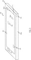
- FIG. 1 illustrates a haptic-enabled device 100 that includes one or more haptic actuators, such as a haptic actuator 110, a haptic actuator 120, and a haptic actuator 130.
- the haptic-enabled device 100 may be a mobile phone or a tablet computer.
- a wearable device e.g., a head-mounted display for a virtual reality context
- game controller e.g., Wii® remote or smart watch
- other user interface device e.g., vehicle dash panel
- the haptic-enabled device 100 may have a housing 101 that houses a display screen 102 (e.g., touch screen), a processor 170, the haptic actuators 110, 120, 130, and other components of the haptic-enabled device 100.
- the haptic actuators 110, 120, and 130 may be disposed at an outer surface 100a of the device 100, such as by being on the outer surface 100a or just below the outer surface 100a.
- the outer surface 100a may include an outer surface 101a of the housing 101 and an outer surface 102a of the display screen 102.
- one or more of the haptic actuators 110, 120, 130 may be attached to the display screen 102, and may be transparent.
- One or more of the haptic actuators 110, 120, 130 may be behind the outer surface 102a of the screen 102, or may alternatively be in front of (e.g., above) the outer surface 102a of the screen 102.
- that actuator may be embedded within the glass or other material of the screen 102.
- the actuator may be located just below the outer surface of the screen 102. In this arrangement, the actuator is not able to directly contact a user's finger or other external object.
- the actuator When one of the haptic actuators is disposed in front of the screen 102, the actuator may be attached (e.g., adhered) to the outer surface of the display screen 102. In this arrangement, the actuator may be able to directly contact a user's finger or other external object.
- haptic actuators 110, 120, 130 may be an electret-based haptic actuator.
- haptic actuator 120 may be an electret-based actuator disposed on or behind (e.g., below) the outer surface 102a of display screen 102
- haptic actuators 120 and 130 may be other electret-based haptic actuators disposed on or behind the outer surface 101a of the housing 101 of the haptic-enabled device 100.
- the haptic actuators 110, 120, 130 may be configured to generate vibrotactile haptic effects at different portions of the haptic-enabled device 100.
- each of the haptic actuators 110, 120, 130 may generate a haptic effect upon receiving a haptic drive signal from a signal generating circuit.
- the haptic actuators 110, 120, 130 may share a signal generating circuit, and/or may be electrically connected to different respective signal generating circuits. If the haptic actuators 110, 120, 130 are configured to share a signal generating circuit, the signal generating circuit may apply the same driving signal to the haptic actuators 110, 120, 130 at the same time, or may switchably apply different driving signals to the haptic actuators 110, 120, 130 in different respective time periods.
- the haptic-enabled device 100 includes a processor 170.
- the processor 170 may be used to control the haptic actuators 110, 120, 130.
- the processor 170 may be a general purpose processor for the haptic-enabled device 100 or a specialized processor, such as a digital signal processor or a processing circuit (e.g., field programmable gate array, or FPGA) dedicated to controlling haptic effects.
- the processor 170 may control and/or implement the signal generating circuit discussed above.
- FIG. 2A provides a perspective view of a haptic actuator 110 in accordance with an embodiment hereof that is situated below an outer surface 100a of a haptic-enabled device, such as haptic enabled device 100.
- the haptic actuator 110 includes an electret layer 112, an electrically conductive layer 118, and a plurality of spacers 114a-114d and an electrically insulative layer 116 placed between the electret layer 112 and the electrically conductive layer 118.
- the electrically conductive layer 118 and the electrically insulative layer 116 may be part of a bi-layer material that is made of at least electrically conductive material of the layer 118 and the electrically insulating material of the layer 116.
- the haptic actuator 110 may be disposed behind the outer surface 100a of the haptic-enabled device 100.
- the outer surface 100a may comprise a thin, flexible electrically insulative layer disposed directly over the haptic actuator 110, such that the outer surface 100a covers the electrically conductive layer 118.
- the outer surface 100a may be an outer surface of a glass that forms the display screen 102, and may embed the haptic actuator 110.
- the outer surface 100a may be used to electrically insulate and/or protect the conductive layer 118 from external objects. While FIG.
- the haptic actuator may have only the spacers 114a-114d to provide a separation between the electrically conductive layer 118 and the electret layer 112, and have no insulative layer 116.
- the electret layer 112 has a permanent electric field arising from a built-in voltage along a thickness dimension T of the layer 112 (i.e., a dimension along which a thickness of the layer 112 is measured, which may be a dimension extending along a direction perpendicular to the layers).
- the built-in voltage may have a value that is, e.g., between 100 V and 1 kV, or between 1 kV and 10 kV, or between 10 kV and 100 kV, or greater than 100 kV.
- the electrically conductive layer 118 may be, e.g., a thin metal sheet
- the electrically insulative layer 116 may be, e.g., a thin polymer film.
- the electret layer 112, the electrically conductive layer 118, and the electrically insulative layer 116 may each form a rectangle having four sides (with two sides along a length dimension L and two sides along a width dimension W). Each of the sides of the respective rectangles may be in a range between 2 mm and 20 mm.
- the side along the length dimension L and the side along the width dimension W of a particular layer may have sizes that are solutions of a multi-physics problem that depends on the size of the layer along the thickness dimension T and the modulus of the layer.
- the size of the layer along its length dimension L and its width dimension W may affect the layer's electrostatic interaction with another layer, but these values may also, along with the size of the layer along its thickness dimension T and the modulus thereof, affect the stiffness of the layer.
- the stiffness and the level of electrostatic interaction may affect the strength of the haptic effect that is output.
- designing the size of the layer along the length dimension L and the width dimension W may take into account the size of the layer along the thickness dimension T and the layer's modulus, and may balance the resulting mechanical stiffness and level of electrostatic interaction to achieve a desired haptic effect output strength.
- each of the layers 112, 116, and 118 may have a thickness that is in a range between 100 microns and 1 mm (i.e., along the thickness dimension T).
- the electrically insulative layer 116 may have a thickness of 1 micron or higher.
- the electret layer 112, electrically insulative layer 116, and the electrically conductive layer 118 may have the same dimensions (and thus the same surface area), or may have different respective dimensions.
- the electrically conductive layer 118 comprises a metal such as copper, aluminum, or a nonconductive material (e.g., plastic or glass) coated with a thin conductive layer (e.g., a gold, indium tin oxide, or conductive nanotube layer), or any combination thereof (e.g., as a metal alloy).
- the electrically conductive layer 118 comprises a nonmetallic conductor, such as graphite or a conductive polymer.
- the electrically conductive layer 118 may have a conductivity that is at least on the order of 10 7 ⁇ .
- the electrically insulative layer 116 comprises plastic, rubber, an insulating polymer (e.g., polyimide), glass, or any other material having a thin coating of an electrically insulative material, such as silicon dioxide or ParyleneTM (poly(p-xylylene)), or any combination thereof.
- the electrically insulative material may have a resistivity that is at least on the order 10 11 ⁇ m.
- the spacers 114a-114d may be used to form a suspension system that creates a space or gap between the electret layer 112 and the conductive layer 118, so as to provide space for the two layers to vibrate relative to each other.
- Example thicknesses of each of the spacers 114a-114d along the dimension T include 0.1 mm, 0.25 mm, or 0.5 mm. Other embodiments may use no spacers, or a different number of spacers (e.g., three spacers, six spacers).
- the spacers 114a-114d may be made of an elastic or rigid (i.e., stiff) material, such as a glass bead (for a stiff suspension), VHBTM tape made from an acrylic elastomer, a silicon-based tape, or polyurethane (all for a softer suspension), or any combination thereof.
- An elastic material may more easily dampen vibrations in the haptic actuator 110, while a rigid material may cause less dampening of vibrations in the haptic actuator 110.
- the level of elasticity or stiffness at which the spacers 114a-114d are made may depend on a level of natural dampening that is desired in the haptic actuator 110. While FIG.
- a spacer may have any other shape that is suitable for the configuration of the actuator.
- each of the spacers 114a-114d may instead have the form of a microdot.
- both the electrically insulative layer 116 and the spacers 114a-114d may be used to prevent the electrically conductive layer 118 and the electret layer 112 from directly touching (e.g., from having plate-to-plate contact) and creating a conductive path between each other. Such contact may cause discharging from the electret layer to the electrically conductive layer.
- the spacers 114a-114d may provide sufficient separation between the conductive layer 118 and the electret layer 112 to prevent them from touching each other, and thus the electrically insulative layer 116 may be omitted.
- a haptic actuator may have additional layers, embodiments of which are discussed below in FIGS. 3 and 4 .
- the haptic actuator may have a layer of adhesive between the other layers (e.g., between electret layer 112 and each of the spacers 114a-114d).
- the conductive layer 118, the electret layer 112, the electrically insulative layer 116, and/or the spacers 114a-114d may be transparent, so as to make the haptic actuator 110 transparent. This transparency renders the actuator 110 more suitable for placement at the display screen 102.
- FIG. 2A further depicts a signal generating circuit 115 that may be electrically connected to the electrically conductive layer 118 and not electrically connected to the electret layer 112.
- the signal generating circuit 115 is part of the haptic-enabled device 100 of FIG. 1 , and may be part of the haptic actuator 110, or may be a separate component.
- the signal generating circuit 115 may be implemented by a processor (e.g., processor 170) of the haptic-enabled device 100.
- the signal generating circuit 115 may be configured to apply an oscillating drive signal, such as a sinusoidal signal or square wave, to the electrically conductive layer 118, at an amplitude that is less than the built-in voltage of the electret layer 112, where the amplitude has a nonzero value.
- the amplitude of the oscillating drive signal may be less than 1/10th of the built-in voltage of the electret layer 112, or less than 1/100th (or 1/1000th) of the built-in voltage of the electret layer 112.
- the electrically conductive layer 118 and/or the electret layer 112 has a resonant vibrating frequency
- the signal generating circuit may be configured to apply an oscillating drive signal at a frequency that is equal to the resonant vibrating frequency of the conductive layer or of the electret layer.
- the oscillating drive signal may have an amplitude that is in the range, e.g., of 1 V to 10 V (or 10 V to 50 V), and a frequency that is in the range, e.g., of 100 Hz to 500 Hz.
- the amplitude of the oscillating drive signal that is generated by the signal generating circuit 115 may be set by processor 170 (or any other control unit) of the haptic-enabled device 100.
- FIG. 2B depicts an embodiment in which the electret layer 112 of the haptic actuator 110 of FIG. 2A is attached to a substrate 140 or other support structure of a haptic-enabled device, such as a substrate 140 of the display screen 102 or the housing 101 of the haptic-enabled device 100.
- the substrate 140 may be considered to be relatively immovable by the haptic actuator 110.
- the electret layer 112 can be considered to be mechanically grounded, and the electrically conductive layer 118 may be considered to be the actuating layer that vibrates when the haptic actuator 110 is activated.
- the vibration of the electrically conductive layer 118 may transfer to the outer surface 100a of the haptic-enabled device 100 to create a vibrotactile haptic effect at the outer surface 100a.
- the haptic actuator 110 may be configured to also function as a sensor. For instance, the haptic actuator 110 may sense a user pressing a portion of the outer surface 100a immediately above the haptic actuator 110. When this portion is pressed, the conductive layer 118 may experience a deformation from a user's touch or other form of input. The deformation may generate a voltage or current signal at the conductive layer 118, or modulate an existing voltage or current signal at the layer 118 to cause a signal change.
- a processor communicatively coupled with the conductive layer 118 e.g., processor 170
- FIG. 2C depicts a sectional view of the haptic actuator 110 along the line A-A in FIG. 2B . More specifically, the sectional view shows the outer surface 100a, electrically conductive layer 118, electrically insulative layer 116, spacers 114c, 114d, electret layer 112, and substrate 140. The sectional view further depicts the permanent electric field 160 from the built-in voltage of the electret layer 112. The figure further illustrates the electric field 160 to arise from a quantity of positive charge and a quantity of negative charge, which have been separated in the electret layer 112. The creation of the electret layer 112 and the electric field 160 of the built-in voltage may be created in numerous ways, which are discussed in more detail below.
- the substrate 140 may have substantially more mass than the haptic actuator 110, and may be considered to be immovable relative to the haptic actuator 110. Accordingly, the electret layer 112 of the haptic actuator 110 in this embodiment may be considered to be mechanically grounded (i.e., mechanically fixed) by the substrate 140, as discussed above. When a driving signal is applied to the electrically conductive layer 118, the mechanically grounded electret layer 112 may be considered to remain stationary, while the electrically conductive layer 118 is an actuating layer that actuates (e.g., vibrates) relative to the electret layer 112.
- the actuation (e.g., vibration) may be transferred to the outer surface 100a to create a haptic effect at the outer surface 100a of the haptic-enabled device 100.
- the electrically insulative layer 116 may move in unison with the conductive layer 118.
- FIG. 3 depicts a sectional view of a haptic actuator (e.g., haptic actuator 120) in accordance with another embodiment hereof that has an electrically conductive layer as the mechanically grounded layer. Further, the conductive layer may be mounted on an outer surface of a haptic-enabled device, such as the outer surface 100a of the haptic-enabled device 100. More specifically, FIG. 3 illustrates a sectional view of a haptic actuator 120 that includes an electrically conductive layer 128, an electrically insulative layer 126, an electret layer 122, and a plurality of spacers (e.g., spacers 124a, 124b) between the electrically conductive layer 128 and the electret layer 122.
- spacers e.g., spacers 124a, 124b
- the haptic actuator 120 further includes a protective layer 123 disposed directly over the electret layer 122.
- the protective layer 123 may be a layer made of an electrically insulative material or any other type of material to electrically insulate and/or protect the electret layer 122 from a user's finger or other external object. In another embodiment, however, the protective layer 123 may be omitted, and the electret layer 122 or another layer may be exposed to the external environment in order to receive a direct touch from an external object.
- FIG. 3 further illustrates a signal generating circuit 125 that is electrically connected to the conductive layer 128 and is configured to apply an oscillating drive signal, or any other drive signal, to the conductive layer 128.
- the signal generating circuit 125 may be part of the haptic actuator 120, or may be an element which is external to the haptic actuator 120.
- the electrically conductive layer 128 may be the mechanically grounded layer.
- the electrically conductive layer 128 may be grounded by being directly attached to the outer surface 100a.
- the outer surface 100a may be an outer surface of a glass layer (e.g., of the display screen 102) or of a plastic layer (e.g., of housing 101) that is more massive than the haptic actuator 120, and is configured to be relatively immovable by the haptic actuator 120.
- a driving signal from the signal generating circuit 125 is applied to the conductive layer 128, the conductive layer 128 may be considered to be stationary, while the electret layer 122 may be the actuating layer that moves relative to the conductive layer 128.
- the conductive layer 128 and the electret layer 122 may alternate between being attracted to each other and being repelled by each other.
- the electret layer 122 may alternate between moving toward the conductive layer 128 and moving away from the conductive layer 128. This motion may vibrate the electret layer 128, and the vibration may be transferred to the protective layer 123 to create a vibrotactile haptic effect.
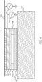
- FIG. 4 illustrates a haptic actuator 130 in accordance with another embodiment hereof that may include two actuating layers. More specifically, the haptic actuator 130 includes an electret layer 132 that is mechanically grounded on a substrate 140, a first actuating layer 138 (e.g., a conductive layer), a second actuating layer 139 (e.g., an electroactive polymer layer or piezoelectric layer) disposed (directly or indirectly) on the first actuating layer 138, and an electrically insulative layer 136 and a plurality of spacers (e.g., 134a, 134b) disposed between the first actuating layer 138 and the electret layer 132.
- FIG. 1 illustrates a haptic actuator 130 in accordance with another embodiment hereof that may include two actuating layers. More specifically, the haptic actuator 130 includes an electret layer 132 that is mechanically grounded on a substrate 140, a first actuating layer 138 (e.g., a
- first signal generating circuit 135 that is electrically connected to the first actuating layer 138
- second signal generating circuit 137 that is electrically connected to the second actuating layer 139.
- Each of the signal generating circuits 135, 137 may be configured to generate an oscillating drive signal or any other drive signal.
- the signal generating circuits 135, 137 may be part of the haptic actuator 130, or may be considered to be external to the haptic actuator 130.
- first actuating layer 138 and the second actuating layer 139 may also enable more complex haptic effects to be generated, because the first actuating layer 138 and the second actuating layer 139 may, in an embodiment, be driven with different respective oscillating drive signals that have different respective amplitudes, frequencies, and/or phases.
- the first signal generating circuit 135 may apply a 100 Hz signal with an amplitude of 5 V to the first actuating layer 138
- the second signal generating circuit 137 may apply a 1 Hz signal with an amplitude of 10 V to the second actuating layer 139.
- the two layers may move differently if they are made of different materials.
- the first actuating layer 138 may be an electrically conductive layer that relies on electrostatic interaction with the electret layer 132 to generate a haptic effect
- the second actuating layer 139 may be an electroactive polymer layer.
- the first actuating layer 138 may be used to generate a vibrotactile haptic effect
- the second actuating layer 139 may be used to generate a more general deformation-based haptic effect.
- FIGS. 5A and 5B illustrate a perspective view and a sectional view of a haptic actuator 150 in accordance with another embodiment hereof that includes a first set of layers 152, 156, 158 and a second set of layers 162, 166, 168, in which the second set of layers 162, 166, 168 are stacked on the first set of layers 152, 156, 158.
- Both sets of the first set of layers 152-158 and the second set of layers 162-168 may be the same layers 112, 116, 118 as those of the haptic actuator 110 in FIG. 2A .
- a haptic actuator with two or more stacked sets of layers may be able to increase its actuation output (e.g., in rate or amount of displacement) compared to a haptic actuator with only one set of layers.
- the motion of the two sets of layers may be synchronized by applying the same drive signal (e.g., same frequency and phase) to both sets of layers.
- the first set of layers in FIGS. 5A and 5B include a first electret layer 152, a first electrically conductive layer 158, a first electrically insulative layer 156 and a first plurality of spacers (e.g., 154a, 154b, 154c) between the first electrically conductive layer 158 and the first electret layer 152.
- the second set of layers includes a second electret layer 162, a second electrically conductive layer 168, a second electrically insulative layer 166 and a second plurality of spacers (e.g., 164a, 164b, 164c) disposed between the second electrically conductive layer 168 and the second electret layer 162.
- the haptic actuator 150 may comprise only the first set and the second set of layers.
- the haptic actuator 150 may comprise additional sets of layers (e.g., a third set of layers, a fourth set of layers, etc.), where the sets of layers are stacked sequentially on top of one another.
- FIGS. 5A and 5B further show a signal generating circuit 155 electrically connected to both the first conductive layer 158 and the second conductive layer 168, and not to any of the electret layers 152, 162.
- the presence of the second set of layers 162-168 may create actuation that supplements the actuation from the first set of layers 152-158.
- the signal generating circuit 155 applies the same oscillating drive signal to the haptic actuator 150 as the signal generating circuit 115 applies to the haptic actuator 110 in FIG. 2A
- the haptic actuator 150 may output a vibrotactile haptic effect that has approximately twice the amplitude as that output by the haptic actuator 110.
- any of the electret layers discussed above may have a permanent or quasi-permanent surface charge and have a built-in voltage that creates an internal and/or external electric field that arises from a built-in voltage.
- the built-in voltage may come from polar domain orientation in the material of the electret layer (e.g., a dielectric material such as a foamed plastic (e.g., polytetrafluoroethylene (PTFE, or TeflonTM), polypropylene, polyethylene terephthalate (PET), polyvinylidene fluoride (PVDF), and their derivatives), silicon dioxide, ParyleneTM, or any combination thereof); come from extra ions or charge in the material; and/or from trapped ions or charge in the material.
- a dielectric material such as a foamed plastic (e.g., polytetrafluoroethylene (PTFE, or TeflonTM), polypropylene, polyethylene terephthalate (PET), polyvinylidene flu
- Extra charge may be inserted into the surface of a dielectric material of the electret layer by using ion discharge techniques, such as corona discharge.
- the corona discharge may be considered as a particle accelerator in which positively or negatively charged particles are accelerated toward a target surface to bombard the surface, and can be trapped inside the material.
- a dielectric polymeric film can be treated via corona discharge to be permanently charged due to the trapped charge.
- the dielectric polymeric film can generate an electric field.
- the direction of the electric field may depend on the nature of the trapped charged particles (e.g., depend on whether they are positively or negatively charged).
- the dielectric polymeric film can be processed into a foam (preferably open cell) to enable it to trap or otherwise absorb more charged particles.
- electret material may also be formed through polar domain orientation.
- This process may involve processing a polar material in a manner that provides the material with non-random molecular polar domains. This may create oriented molecular dipoles that can generate a net electric field.
- One way of creating the non-random molecular polar domains involves heating a material to a temperature at which dipoles in the material can freely rotate. Then, a strong external electric field may be applied to the material, and the material may then be allowed to cool in a controlled manner while maintaining the external electric field. As a result, the dipoles may be frozen along a direction of the external electric field, and a net electric field results from the oriented molecular dipoles inside the material.
- the electric field of an electret layer is from the presence of permanent, trapped charge in the layer, and the electret layer is arranged in a parallel plate configuration with an electrically conductive layer
- E the strength of the electric field
- Q the amount of excess charge trapped in the electret layer
- A an area of the electret layer
- ⁇ is a charge density
- ⁇ o is the dielectric permittivity constant.
- the electret-based haptic actuator of the embodiments herein may be used in any context, such as in a gaming, automotive, wearable, virtual reality or augmented reality, or other user interface context.
Landscapes
- Engineering & Computer Science (AREA)
- General Engineering & Computer Science (AREA)
- Theoretical Computer Science (AREA)
- Human Computer Interaction (AREA)
- Physics & Mathematics (AREA)
- General Physics & Mathematics (AREA)
- User Interface Of Digital Computer (AREA)
- Apparatuses For Generation Of Mechanical Vibrations (AREA)
Applications Claiming Priority (1)
| Application Number | Priority Date | Filing Date | Title |
|---|---|---|---|
| US15/461,875 US10581343B2 (en) | 2017-03-17 | 2017-03-17 | Electret-based electrostatic haptic actuator |
Publications (2)
| Publication Number | Publication Date |
|---|---|
| EP3376346A2 true EP3376346A2 (de) | 2018-09-19 |
| EP3376346A3 EP3376346A3 (de) | 2018-10-10 |
Family
ID=61873269
Family Applications (1)
| Application Number | Title | Priority Date | Filing Date |
|---|---|---|---|
| EP18162335.6A Withdrawn EP3376346A3 (de) | 2017-03-17 | 2018-03-16 | Elektrostatischer elektret-basierter haptischer aktuator |
Country Status (5)
| Country | Link |
|---|---|
| US (1) | US10581343B2 (de) |
| EP (1) | EP3376346A3 (de) |
| JP (1) | JP2018156651A (de) |
| KR (1) | KR20180106918A (de) |
| CN (1) | CN108628438A (de) |
Families Citing this family (14)
| Publication number | Priority date | Publication date | Assignee | Title |
|---|---|---|---|---|
| US20180329493A1 (en) * | 2017-05-11 | 2018-11-15 | Immersion Corporation | Microdot Actuators |
| US10416772B2 (en) | 2017-09-06 | 2019-09-17 | Apple Inc. | Electrical haptic output array |
| US10775890B2 (en) | 2017-09-27 | 2020-09-15 | Apple Inc. | Electronic device having a piezoelectric body for friction haptics |
| US10585482B2 (en) * | 2017-09-27 | 2020-03-10 | Apple Inc. | Electronic device having a hybrid conductive coating for electrostatic haptics |
| US10248211B1 (en) | 2017-09-28 | 2019-04-02 | Apple Inc. | Ground-shifted touch input sensor for capacitively driving an electrostatic plate |
| US10395489B1 (en) * | 2018-06-15 | 2019-08-27 | Immersion Corporation | Generation and braking of vibrations |
| US11139756B2 (en) * | 2018-12-11 | 2021-10-05 | Facebook Technologies, Llc | Transducers with electrostatic repulsion and associated systems and methods |
| US11347312B1 (en) * | 2019-09-23 | 2022-05-31 | Apple Inc. | Ultrasonic haptic output devices |
| KR102834654B1 (ko) | 2019-12-17 | 2025-07-16 | 삼성디스플레이 주식회사 | 표시 장치와 그의 햅틱 피드백 방법 |
| US12223110B1 (en) | 2021-09-23 | 2025-02-11 | Apple Inc. | Secure integrated circuit for smart haptics |
| CN116455263A (zh) * | 2023-04-21 | 2023-07-18 | 中山大学 | 提供触觉反馈的柔性振动电机、触觉反馈系统及电子设备 |
| US12333077B2 (en) * | 2023-04-21 | 2025-06-17 | Sun Yat-Sen University | Flexible vibration motor for providing tactile feedback, tactile feedback system and electronic device |
| KR20250177206A (ko) * | 2024-06-14 | 2025-12-23 | 한국과학기술원 | 구역 별로 개별 전류 제어가 가능한 메타구조 직물형 액추에이터의 제조 방법 및 그 직물형 액추에이터 |
| CN120767076B (zh) * | 2025-09-08 | 2025-11-21 | 国网湖北省电力有限公司襄阳供电公司 | 模块化组合式电力设备用绝缘子组件 |
Family Cites Families (7)
| Publication number | Priority date | Publication date | Assignee | Title |
|---|---|---|---|---|
| EP1662308A4 (de) | 2003-08-21 | 2011-03-02 | Olympus Corp | Elektrostatisches stellglied, blendeneinrichtung, abbildungsmodul und kamera |
| JP2006025578A (ja) | 2004-07-09 | 2006-01-26 | Olympus Corp | エレクトレットアクチュエータ |
| US7740563B2 (en) | 2004-08-11 | 2010-06-22 | Icon Ip, Inc. | Elliptical exercise machine with integrated anaerobic exercise system |
| JP4802998B2 (ja) * | 2005-12-19 | 2011-10-26 | セイコーエプソン株式会社 | 静電型超音波トランスデューサの駆動制御方法、静電型超音波トランスデューサ、これを用いた超音波スピーカ、音声信号再生方法、超指向性音響システム及び表示装置 |
| WO2009125773A1 (ja) * | 2008-04-07 | 2009-10-15 | 国立大学法人埼玉大学 | 機械電気変換素子、機械電気変換装置及びその製造方法 |
| US8411882B2 (en) * | 2008-10-31 | 2013-04-02 | Htc Corporation | Electronic device with electret electro-acoustic transducer |
| US10966006B2 (en) * | 2010-12-31 | 2021-03-30 | Nokia Technologies Oy | Apparatus and method for a sound generating device combined with a display unit |
-
2017
- 2017-03-17 US US15/461,875 patent/US10581343B2/en not_active Expired - Fee Related
-
2018
- 2018-03-14 KR KR1020180029627A patent/KR20180106918A/ko not_active Withdrawn
- 2018-03-15 JP JP2018047454A patent/JP2018156651A/ja active Pending
- 2018-03-16 CN CN201810216001.8A patent/CN108628438A/zh active Pending
- 2018-03-16 EP EP18162335.6A patent/EP3376346A3/de not_active Withdrawn
Non-Patent Citations (1)
| Title |
|---|
| None |
Also Published As
| Publication number | Publication date |
|---|---|
| US20180269807A1 (en) | 2018-09-20 |
| KR20180106918A (ko) | 2018-10-01 |
| CN108628438A (zh) | 2018-10-09 |
| US10581343B2 (en) | 2020-03-03 |
| EP3376346A3 (de) | 2018-10-10 |
| JP2018156651A (ja) | 2018-10-04 |
Similar Documents
| Publication | Publication Date | Title |
|---|---|---|
| US10581343B2 (en) | Electret-based electrostatic haptic actuator | |
| US11573661B2 (en) | Electronic device having a piezoelectric body for friction haptics | |
| US9122325B2 (en) | Touch interface device and method for applying controllable shear forces to a human appendage | |
| TWI631494B (zh) | 接觸敏感裝置、包含所述接觸敏感裝置的顯示設備及顯示設備製造方法 | |
| US11073934B2 (en) | Electronic device having an electrostatic conductive layer for providing haptic feedback | |
| CN107077194B (zh) | 磁性触觉提供装置 | |
| US7868515B2 (en) | Thin laminate construction for the creation of tactile feedback | |
| US20120139850A1 (en) | Haptic driving assembly and electronic device using the same | |
| KR102770878B1 (ko) | 표시 장치 | |
| CN101882023B (zh) | 具有振动功能的触控显示装置及振动式触控板 | |
| US20210232308A1 (en) | Systems, devices, and methods for providing localized haptic effects | |
| CN107077198A (zh) | 电子设备 | |
| KR101632665B1 (ko) | 표면형 디스플레이 장치 및 방법 | |
| US10108288B2 (en) | Touch interface device and method for applying controllable shear forces to a human appendage | |
| Kamigaki et al. | Thin and flexible airborne ultrasound phased array for tactile display | |
| KR101587338B1 (ko) | 정전기력 기반의 폴리머 액추에이터를 이용한 플렉서블 햅틱모듈 및 촉감제공방법 | |
| CN117472175A (zh) | 一种触觉反馈显示模组和显示装置 | |
| CN108737942A (zh) | 声波生成装置 | |
| KR101610794B1 (ko) | 도전성 폴리머 층을 포함한 정전기력 기반 작동기 | |
| KR102313293B1 (ko) | 액츄에이터, 액츄에이터 구동 방법 및 액츄에이터를 포함하는 표시 장치 | |
| Lim et al. | Force and displacement analysis of a haptic touchscreen | |
| Lee et al. | Transparent and Soft Vibrotactile Actuator Based on Silicone Rubber |
Legal Events
| Date | Code | Title | Description |
|---|---|---|---|
| PUAI | Public reference made under article 153(3) epc to a published international application that has entered the european phase |
Free format text: ORIGINAL CODE: 0009012 |
|
| PUAL | Search report despatched |
Free format text: ORIGINAL CODE: 0009013 |
|
| AK | Designated contracting states |
Kind code of ref document: A2 Designated state(s): AL AT BE BG CH CY CZ DE DK EE ES FI FR GB GR HR HU IE IS IT LI LT LU LV MC MK MT NL NO PL PT RO RS SE SI SK SM TR |
|
| AX | Request for extension of the european patent |
Extension state: BA ME |
|
| AK | Designated contracting states |
Kind code of ref document: A3 Designated state(s): AL AT BE BG CH CY CZ DE DK EE ES FI FR GB GR HR HU IE IS IT LI LT LU LV MC MK MT NL NO PL PT RO RS SE SI SK SM TR |
|
| AX | Request for extension of the european patent |
Extension state: BA ME |
|
| RIC1 | Information provided on ipc code assigned before grant |
Ipc: G06F 3/01 20060101AFI20180906BHEP Ipc: A63F 13/285 20140101ALI20180906BHEP Ipc: G06F 3/041 20060101ALI20180906BHEP |
|
| 17P | Request for examination filed |
Effective date: 20190408 |
|
| RBV | Designated contracting states (corrected) |
Designated state(s): AL AT BE BG CH CY CZ DE DK EE ES FI FR GB GR HR HU IE IS IT LI LT LU LV MC MK MT NL NO PL PT RO RS SE SI SK SM TR |
|
| GRAP | Despatch of communication of intention to grant a patent |
Free format text: ORIGINAL CODE: EPIDOSNIGR1 |
|
| INTG | Intention to grant announced |
Effective date: 20200110 |
|
| STAA | Information on the status of an ep patent application or granted ep patent |
Free format text: STATUS: THE APPLICATION IS DEEMED TO BE WITHDRAWN |
|
| 18D | Application deemed to be withdrawn |
Effective date: 20200603 |