EP3376535A1 - Semiconductor package structure - Google Patents
Semiconductor package structure Download PDFInfo
- Publication number
- EP3376535A1 EP3376535A1 EP18160366.3A EP18160366A EP3376535A1 EP 3376535 A1 EP3376535 A1 EP 3376535A1 EP 18160366 A EP18160366 A EP 18160366A EP 3376535 A1 EP3376535 A1 EP 3376535A1
- Authority
- EP
- European Patent Office
- Prior art keywords
- hole
- substrate
- semiconductor die
- package structure
- semiconductor
- Prior art date
- Legal status (The legal status is an assumption and is not a legal conclusion. Google has not performed a legal analysis and makes no representation as to the accuracy of the status listed.)
- Granted
Links
Images


Classifications
-
- H—ELECTRICITY
- H10—SEMICONDUCTOR DEVICES; ELECTRIC SOLID-STATE DEVICES NOT OTHERWISE PROVIDED FOR
- H10W—GENERIC PACKAGES, INTERCONNECTIONS, CONNECTORS OR OTHER CONSTRUCTIONAL DETAILS OF DEVICES COVERED BY CLASS H10
- H10W42/00—Arrangements for protection of devices
- H10W42/121—Arrangements for protection of devices protecting against mechanical damage
-
- H—ELECTRICITY
- H05—ELECTRIC TECHNIQUES NOT OTHERWISE PROVIDED FOR
- H05K—PRINTED CIRCUITS; CASINGS OR CONSTRUCTIONAL DETAILS OF ELECTRIC APPARATUS; MANUFACTURE OF ASSEMBLAGES OF ELECTRICAL COMPONENTS
- H05K1/00—Printed circuits
- H05K1/02—Details
- H05K1/0271—Arrangements for reducing stress or warp in rigid printed circuit boards, e.g. caused by loads, vibrations or differences in thermal expansion
-
- H—ELECTRICITY
- H10—SEMICONDUCTOR DEVICES; ELECTRIC SOLID-STATE DEVICES NOT OTHERWISE PROVIDED FOR
- H10W—GENERIC PACKAGES, INTERCONNECTIONS, CONNECTORS OR OTHER CONSTRUCTIONAL DETAILS OF DEVICES COVERED BY CLASS H10
- H10W70/00—Package substrates; Interposers; Redistribution layers [RDL]
- H10W70/60—Insulating or insulated package substrates; Interposers; Redistribution layers
- H10W70/611—Insulating or insulated package substrates; Interposers; Redistribution layers for connecting multiple chips together
-
- H—ELECTRICITY
- H10—SEMICONDUCTOR DEVICES; ELECTRIC SOLID-STATE DEVICES NOT OTHERWISE PROVIDED FOR
- H10W—GENERIC PACKAGES, INTERCONNECTIONS, CONNECTORS OR OTHER CONSTRUCTIONAL DETAILS OF DEVICES COVERED BY CLASS H10
- H10W70/00—Package substrates; Interposers; Redistribution layers [RDL]
- H10W70/60—Insulating or insulated package substrates; Interposers; Redistribution layers
- H10W70/62—Insulating or insulated package substrates; Interposers; Redistribution layers characterised by their interconnections
- H10W70/65—Shapes or dispositions of interconnections
-
- H—ELECTRICITY
- H10—SEMICONDUCTOR DEVICES; ELECTRIC SOLID-STATE DEVICES NOT OTHERWISE PROVIDED FOR
- H10W—GENERIC PACKAGES, INTERCONNECTIONS, CONNECTORS OR OTHER CONSTRUCTIONAL DETAILS OF DEVICES COVERED BY CLASS H10
- H10W70/00—Package substrates; Interposers; Redistribution layers [RDL]
- H10W70/60—Insulating or insulated package substrates; Interposers; Redistribution layers
- H10W70/67—Insulating or insulated package substrates; Interposers; Redistribution layers characterised by their insulating layers or insulating parts
- H10W70/68—Shapes or dispositions thereof
-
- H—ELECTRICITY
- H10—SEMICONDUCTOR DEVICES; ELECTRIC SOLID-STATE DEVICES NOT OTHERWISE PROVIDED FOR
- H10W—GENERIC PACKAGES, INTERCONNECTIONS, CONNECTORS OR OTHER CONSTRUCTIONAL DETAILS OF DEVICES COVERED BY CLASS H10
- H10W70/00—Package substrates; Interposers; Redistribution layers [RDL]
- H10W70/60—Insulating or insulated package substrates; Interposers; Redistribution layers
- H10W70/67—Insulating or insulated package substrates; Interposers; Redistribution layers characterised by their insulating layers or insulating parts
- H10W70/68—Shapes or dispositions thereof
- H10W70/685—Shapes or dispositions thereof comprising multiple insulating layers
-
- H—ELECTRICITY
- H10—SEMICONDUCTOR DEVICES; ELECTRIC SOLID-STATE DEVICES NOT OTHERWISE PROVIDED FOR
- H10W—GENERIC PACKAGES, INTERCONNECTIONS, CONNECTORS OR OTHER CONSTRUCTIONAL DETAILS OF DEVICES COVERED BY CLASS H10
- H10W72/00—Interconnections or connectors in packages
- H10W72/20—Bump connectors, e.g. solder bumps or copper pillars; Dummy bumps; Thermal bumps
-
- H—ELECTRICITY
- H10—SEMICONDUCTOR DEVICES; ELECTRIC SOLID-STATE DEVICES NOT OTHERWISE PROVIDED FOR
- H10W—GENERIC PACKAGES, INTERCONNECTIONS, CONNECTORS OR OTHER CONSTRUCTIONAL DETAILS OF DEVICES COVERED BY CLASS H10
- H10W74/00—Encapsulations, e.g. protective coatings
- H10W74/10—Encapsulations, e.g. protective coatings characterised by their shape or disposition
- H10W74/111—Encapsulations, e.g. protective coatings characterised by their shape or disposition the semiconductor body being completely enclosed
- H10W74/121—Encapsulations, e.g. protective coatings characterised by their shape or disposition the semiconductor body being completely enclosed by multiple encapsulations, e.g. by a thin protective coating and a thick encapsulation
-
- H—ELECTRICITY
- H10—SEMICONDUCTOR DEVICES; ELECTRIC SOLID-STATE DEVICES NOT OTHERWISE PROVIDED FOR
- H10W—GENERIC PACKAGES, INTERCONNECTIONS, CONNECTORS OR OTHER CONSTRUCTIONAL DETAILS OF DEVICES COVERED BY CLASS H10
- H10W76/00—Containers; Fillings or auxiliary members therefor; Seals
- H10W76/10—Containers or parts thereof
- H10W76/12—Containers or parts thereof characterised by their shape
- H10W76/13—Containers comprising a conductive base serving as an interconnection
-
- H—ELECTRICITY
- H10—SEMICONDUCTOR DEVICES; ELECTRIC SOLID-STATE DEVICES NOT OTHERWISE PROVIDED FOR
- H10W—GENERIC PACKAGES, INTERCONNECTIONS, CONNECTORS OR OTHER CONSTRUCTIONAL DETAILS OF DEVICES COVERED BY CLASS H10
- H10W90/00—Package configurations
-
- H—ELECTRICITY
- H10—SEMICONDUCTOR DEVICES; ELECTRIC SOLID-STATE DEVICES NOT OTHERWISE PROVIDED FOR
- H10W—GENERIC PACKAGES, INTERCONNECTIONS, CONNECTORS OR OTHER CONSTRUCTIONAL DETAILS OF DEVICES COVERED BY CLASS H10
- H10W90/00—Package configurations
- H10W90/701—Package configurations characterised by the relative positions of pads or connectors relative to package parts
-
- H—ELECTRICITY
- H10—SEMICONDUCTOR DEVICES; ELECTRIC SOLID-STATE DEVICES NOT OTHERWISE PROVIDED FOR
- H10W—GENERIC PACKAGES, INTERCONNECTIONS, CONNECTORS OR OTHER CONSTRUCTIONAL DETAILS OF DEVICES COVERED BY CLASS H10
- H10W70/00—Package substrates; Interposers; Redistribution layers [RDL]
- H10W70/60—Insulating or insulated package substrates; Interposers; Redistribution layers
- H10W70/62—Insulating or insulated package substrates; Interposers; Redistribution layers characterised by their interconnections
- H10W70/63—Vias, e.g. via plugs
-
- H—ELECTRICITY
- H10—SEMICONDUCTOR DEVICES; ELECTRIC SOLID-STATE DEVICES NOT OTHERWISE PROVIDED FOR
- H10W—GENERIC PACKAGES, INTERCONNECTIONS, CONNECTORS OR OTHER CONSTRUCTIONAL DETAILS OF DEVICES COVERED BY CLASS H10
- H10W70/00—Package substrates; Interposers; Redistribution layers [RDL]
- H10W70/60—Insulating or insulated package substrates; Interposers; Redistribution layers
- H10W70/67—Insulating or insulated package substrates; Interposers; Redistribution layers characterised by their insulating layers or insulating parts
- H10W70/68—Shapes or dispositions thereof
- H10W70/681—Shapes or dispositions thereof comprising holes not having chips therein, e.g. for outgassing, underfilling or bond wire passage
-
- H—ELECTRICITY
- H10—SEMICONDUCTOR DEVICES; ELECTRIC SOLID-STATE DEVICES NOT OTHERWISE PROVIDED FOR
- H10W—GENERIC PACKAGES, INTERCONNECTIONS, CONNECTORS OR OTHER CONSTRUCTIONAL DETAILS OF DEVICES COVERED BY CLASS H10
- H10W72/00—Interconnections or connectors in packages
- H10W72/071—Connecting or disconnecting
- H10W72/072—Connecting or disconnecting of bump connectors
-
- H—ELECTRICITY
- H10—SEMICONDUCTOR DEVICES; ELECTRIC SOLID-STATE DEVICES NOT OTHERWISE PROVIDED FOR
- H10W—GENERIC PACKAGES, INTERCONNECTIONS, CONNECTORS OR OTHER CONSTRUCTIONAL DETAILS OF DEVICES COVERED BY CLASS H10
- H10W72/00—Interconnections or connectors in packages
- H10W72/071—Connecting or disconnecting
- H10W72/073—Connecting or disconnecting of die-attach connectors
-
- H—ELECTRICITY
- H10—SEMICONDUCTOR DEVICES; ELECTRIC SOLID-STATE DEVICES NOT OTHERWISE PROVIDED FOR
- H10W—GENERIC PACKAGES, INTERCONNECTIONS, CONNECTORS OR OTHER CONSTRUCTIONAL DETAILS OF DEVICES COVERED BY CLASS H10
- H10W72/00—Interconnections or connectors in packages
- H10W72/851—Dispositions of multiple connectors or interconnections
- H10W72/874—On different surfaces
-
- H—ELECTRICITY
- H10—SEMICONDUCTOR DEVICES; ELECTRIC SOLID-STATE DEVICES NOT OTHERWISE PROVIDED FOR
- H10W—GENERIC PACKAGES, INTERCONNECTIONS, CONNECTORS OR OTHER CONSTRUCTIONAL DETAILS OF DEVICES COVERED BY CLASS H10
- H10W72/00—Interconnections or connectors in packages
- H10W72/851—Dispositions of multiple connectors or interconnections
- H10W72/874—On different surfaces
- H10W72/877—Bump connectors and die-attach connectors
-
- H—ELECTRICITY
- H10—SEMICONDUCTOR DEVICES; ELECTRIC SOLID-STATE DEVICES NOT OTHERWISE PROVIDED FOR
- H10W—GENERIC PACKAGES, INTERCONNECTIONS, CONNECTORS OR OTHER CONSTRUCTIONAL DETAILS OF DEVICES COVERED BY CLASS H10
- H10W74/00—Encapsulations, e.g. protective coatings
- H10W74/10—Encapsulations, e.g. protective coatings characterised by their shape or disposition
- H10W74/131—Encapsulations, e.g. protective coatings characterised by their shape or disposition the semiconductor body being only partially enclosed
- H10W74/142—Encapsulations, e.g. protective coatings characterised by their shape or disposition the semiconductor body being only partially enclosed the encapsulations exposing the passive side of the semiconductor body
-
- H—ELECTRICITY
- H10—SEMICONDUCTOR DEVICES; ELECTRIC SOLID-STATE DEVICES NOT OTHERWISE PROVIDED FOR
- H10W—GENERIC PACKAGES, INTERCONNECTIONS, CONNECTORS OR OTHER CONSTRUCTIONAL DETAILS OF DEVICES COVERED BY CLASS H10
- H10W74/00—Encapsulations, e.g. protective coatings
- H10W74/10—Encapsulations, e.g. protective coatings characterised by their shape or disposition
- H10W74/15—Encapsulations, e.g. protective coatings characterised by their shape or disposition on active surfaces of flip-chip devices, e.g. underfills
-
- H—ELECTRICITY
- H10—SEMICONDUCTOR DEVICES; ELECTRIC SOLID-STATE DEVICES NOT OTHERWISE PROVIDED FOR
- H10W—GENERIC PACKAGES, INTERCONNECTIONS, CONNECTORS OR OTHER CONSTRUCTIONAL DETAILS OF DEVICES COVERED BY CLASS H10
- H10W90/00—Package configurations
- H10W90/401—Package configurations characterised by multiple insulating or insulated package substrates, interposers or RDLs
-
- H—ELECTRICITY
- H10—SEMICONDUCTOR DEVICES; ELECTRIC SOLID-STATE DEVICES NOT OTHERWISE PROVIDED FOR
- H10W—GENERIC PACKAGES, INTERCONNECTIONS, CONNECTORS OR OTHER CONSTRUCTIONAL DETAILS OF DEVICES COVERED BY CLASS H10
- H10W90/00—Package configurations
- H10W90/701—Package configurations characterised by the relative positions of pads or connectors relative to package parts
- H10W90/721—Package configurations characterised by the relative positions of pads or connectors relative to package parts of bump connectors
- H10W90/724—Package configurations characterised by the relative positions of pads or connectors relative to package parts of bump connectors between a chip and a stacked insulating package substrate, interposer or RDL
-
- H—ELECTRICITY
- H10—SEMICONDUCTOR DEVICES; ELECTRIC SOLID-STATE DEVICES NOT OTHERWISE PROVIDED FOR
- H10W—GENERIC PACKAGES, INTERCONNECTIONS, CONNECTORS OR OTHER CONSTRUCTIONAL DETAILS OF DEVICES COVERED BY CLASS H10
- H10W90/00—Package configurations
- H10W90/701—Package configurations characterised by the relative positions of pads or connectors relative to package parts
- H10W90/731—Package configurations characterised by the relative positions of pads or connectors relative to package parts of die-attach connectors
- H10W90/734—Package configurations characterised by the relative positions of pads or connectors relative to package parts of die-attach connectors between a chip and a stacked insulating package substrate, interposer or RDL
Definitions
- the present invention relates to a semiconductor package structure, and in particular to a semiconductor package structure with holes formed on a top surface of a substrate therein.
- a semiconductor package can not only provide a semiconductor die with protection from environmental contaminants, but it can also provide an electrical connection between the semiconductor die packaged therein and a substrate, such as a printed circuit board (PCB).
- a semiconductor die may be enclosed in an encapsulating material, and traces are electrically connected to the semiconductor die and the substrate.
- a problem with such a semiconductor package is that it is subject to different temperatures during the packaging process.
- the semiconductor package may be highly stressed due to the different coefficients of thermal expansion (CTEs) of the various substrate and semiconductor die materials.
- CTEs coefficients of thermal expansion
- the semiconductor package may exhibit warping or cracking so that the electrical connection between the semiconductor die and the substrate may be damaged, and the reliability of the semiconductor package may be decreased.
- An exemplary embodiment of a semiconductor package structure includes a substrate having a first surface and a second surface opposite thereto.
- the substrate includes a wiring structure.
- the semiconductor package structure also includes a first semiconductor die disposed over the first surface of the substrate and electrically coupled to the wiring structure.
- the semiconductor package structure further includes a second semiconductor die disposed over the first surface of the substrate and electrically coupled to the wiring structure.
- the first semiconductor die and the second semiconductor die are separated by a molding material.
- the semiconductor package structure includes a first hole and a second hole formed on the second surface of the substrate.
- a semiconductor package structure includes a substrate having a wiring structure.
- the semiconductor package structure also includes a first semiconductor die disposed over the substrate and electrically coupled to the wiring structure.
- the semiconductor package structure further includes a second semiconductor die disposed over the substrate and electrically coupled to the wiring structure.
- the first semiconductor die and the second semiconductor die are arranged side-by-side.
- the semiconductor package structure includes a plurality of holes formed on a surface of the substrate. The holes are located within projections of the first semiconductor die and the second semiconductor die on the substrate.
- a substrate structure includes a wiring structure disposed in a substrate, wherein the wiring structure is coupled to a plurality of semiconductor dies disposed over the substrate.
- the substrate structure also includes a plurality of holes formed on a surface of the substrate, wherein the holes are located within projections of the semiconductor die on the substrate.
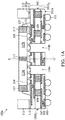
- Fig. 1A is a cross-sectional view of a semiconductor package structure 100a, in accordance with some embodiments of the disclosure.
- Fig. 1C is a plan view of an arrangement of holes in a substrate 101 of the semiconductor package structure 100a shown in Fig. 1A
- Fig. 1A is a cross-sectional view of the semiconductor package structure 100a along line I-I' of Fig.1C .
- the semiconductor package structure 100a may include a wafer-level semiconductor package, for example, a flip-chip semiconductor package.
- the semiconductor package structure 100a may be mounted on a base (not shown).
- the semiconductor package structure 100a may be a system-on-chip (SOC) package structure.
- the base may include a printed circuit board (PCB) and may be formed of polypropylene (PP).
- the base may include a package substrate.
- the semiconductor package structure 100a is mounted on the base by a bonding process.
- the semiconductor package structure 100a includes bump structures 111.
- the bump structures 111 may be conductive ball structures (such as ball grid array (BGA)), conductive pillar structures, or conductive paste structures that are mounted on and electrically coupled to the base by the bonding process.
- the semiconductor package structure 100a includes a substrate 101.
- the substrate 101 has a wiring structure therein.
- the wiring structure in the substrate 101 is a fan-out structure, and may include one or more conductive pads 103, conductive vias 105, conductive layers 107 and conductive pillars 109.
- the wiring structure in the substrate 101 may be disposed in one or more intermetal dielectric (IMD) layers.
- the IMD layers may be formed of organic materials, which include a polymer base material, non-organic materials, which include silicon nitride (SiN x ), silicon oxide (SiO x ), grapheme, or the like.
- the IMD layers are made of a polymer base material. It should be noted that the number and configuration of the IMD layers, the conductive pads 103, the conductive vias 105, the conductive layers 107 and the conductive pillars 109 shown in Figures and only some examples and are not limitations to the present invention.
- the semiconductor package structure 100a also includes a first semiconductor die 115a and a second semiconductor die 115b bonded onto the substrate 101 through a plurality of conductive structures 119.
- the substrate 101 has a first surface 101a and a second surface 101b opposite thereto, the first surface 101a is facing the first semiconductor die 115a and the second semiconductor die 115b, and the second surface 101b is facing the above-mentioned base.
- the conductive structures 119 are disposed over the first surface 101a and below the first semiconductor die 115a and the second semiconductor die 115b, and the bump structures 111 are disposed over the second surface 101b of the substrate 101.
- the first semiconductor die 115a and the second semiconductor die 115b are electrically coupled to the bump structures 111 through the conductive structures 119 and the wiring structure in the substrate 101.
- the conductive structures 119 may be controlled collapse chip connection (C4) structures. It should be noted that the number of semiconductor dies integrated in the semiconductor package structure 100a is not limited to that disclosed in the embodiment.
- the first semiconductor die 115a and the second semiconductor die 115b are active devices.
- the first semiconductor die 115a and the second semiconductor die 115b may be logic dies including a central processing unit (CPU), a graphics processing unit (GPU), a dynamic random access memory (DRAM) controller or any combination thereof.
- one or more passive devices are also bonded onto the substrate 101.
- the first semiconductor die 115a and the second semiconductor dies 115b are arranged side-by-side. In some embodiments, the first semiconductor die 115a and the second semiconductor dies 115b are separated by a molding material 117.
- the molding material 117 surrounds the first semiconductor die 115a and the second semiconductor die 115b, and adjoins the sidewalls of the first semiconductor die 115a and the second semiconductor die 115b.
- the molding material 117 includes a nonconductive material such as an epoxy, a resin, a moldable polymer, or another suitable molding material. In some embodiments, the molding material 117 is applied as a substantial liquid, and then is cured through a chemical reaction.
- the molding material 117 is an ultraviolet (UV) or thermally cured polymer applied as a gel or malleable solid, and then is cured through a UV or thermal curing process.
- the molding material 117 may be cured with a mold (not shown).
- the surfaces of the first semiconductor die 115a and the second semiconductor dies 115b facing away from the first surface 101a of the substrate 101 are exposed by the molding material 117, such that a heat dissipating device (not shown) can directly attached to the surfaces of the first semiconductor die 115a and the second semiconductor dies 115b.
- a heat dissipating device (not shown) can directly attached to the surfaces of the first semiconductor die 115a and the second semiconductor dies 115b.
- the semiconductor package structure 100a also includes a polymer material 121 disposed under the molding material 117, the first semiconductor die 115a and the second semiconductor die 115b, and between the conductive structures 119.
- the semiconductor package structure 100a further includes an underfill layer 123 interposed between the first surface 101a of the substrate 101 and the polymer material 121.
- the first semiconductor die 115a, the second semiconductor dies 115b and the molding material 117 are surrounded by the underfill layer 123.
- the polymer material 121 and the underfill layer 123 are disposed to compensate for differing coefficients of thermal expansion (CTEs) between the substrate 101, the conductive structures 119, the first semiconductor die 115a and the second semiconductor dies 115b.
- CTEs coefficients of thermal expansion
- the semiconductor package structure 100a includes a frame 113 attached to the first surface 101a of the substrate 101 through an adhesive layer 112.
- the first semiconductor die 115a and the second semiconductor die 115b are surrounded by the frame 113 and the adhesive layer 112.
- the frame 113 and the adhesive layer 112 are separated from the underfill layer 121 by a gap.
- the substrate 101 has a first edge 101E 1 and a second edge 101E 2 opposite thereto.
- the first edge 101 E 1 and the second edge 101E 2 are coplanar with sidewalls of the frame 113 and the adhesive layer 112.
- the substrate 101 of the semiconductor package structure 100a includes a first hole 110a and a second hole 110b formed on the second surface 101b.
- at least one of the first hole 110a and the second hole 110b penetrates through the substrate 101 from the first surface 101a to the second surface 101b.
- both the first hole 110a and the second hole 110b shown in Fig. 1A penetrate through the substrate 101, in some other embodiments, both the first hole 110a and the second hole 110b do not penetrate through the substrate 101 from the first surface 101a to the second surface 101b.
- the first hole 110a is covered by the first semiconductor die 115a
- the second hole 110b is covered by the second semiconductor die 115b.
- the first hole 110a is located within the projection of the first semiconductor die 115a on the substrate 101
- the second hole 110b is located within the projection of the second semiconductor die 115b on the substrate 101.
- the first semiconductor die 115a and the second semiconductor die 115b have a center line C-C' between them.
- the first hole 110a is disposed closer to the center line C-C' than the first edge 101E 1 of the substrate 101
- the second hole 110b is disposed closer to the center line C-C' than the second edge 101E 2 of the substrate 101.
- the first hole 110a and the second hole 110b are formed by a laser drilling process or another suitable process. It should be noted that the first hole 110a and the second hole 110b may be formed by the same forming process for the conductive pillars 109 in the wiring structure of the substrate 101. Moreover, the first semiconductor die 115a and the second semiconductor die 115b are bonded to the substrate 101 after forming the holes in the substrate 101. Therefore, the damage of the first semiconductor die 115a and the second semiconductor die 115b can be prevented.
- Fig. 1C is a plan view of an arrangement of holes in a substrate 101 of the semiconductor package structure 100a shown in Fig. 1A
- Fig. 1A is a cross-sectional view of the semiconductor package structure 100a along line I-I' of Fig. 1C
- Fig. 1C is the plan view from the bottom of the semiconductor package structure 100a.
- Fig. 1C is the plan view from the second surface 101b of the substrate 101, which the bump structures 111 are disposed on.
- the bump structures 111 are omitted for brevity.
- the substrate 101 includes more than two holes.
- the substrate 101 further includes a third hole 110c and the fourth hole 110d formed on the second surface 101b.
- the third hole 110c is covered by the first semiconductor die 115a
- the fourth hole 110d is covered by the second semiconductor die 115b.
- the substrate 101 has a center 101C, and the first hole 101a, the second hole 101b, the third hole 110c, and the fourth hole 110d are disposed closer to the center 101C than the first edge 101E 1 and the second edge 101E 2 of the substrate 101.
- the holes formed in the substrate 101 are designed to release the stress in the substrate 101, especially the stress concentrated in the region below the interface between two semiconductor dies (i.e. the first semiconductor die 115a and the second semiconductor die 115b). Since the semiconductor package structure 100a may be highly stressed due to the different coefficients of thermal expansion (CTEs) of the substrate 101 and the semiconductor dies, the holes formed in the substrate 101 can solve the warping or cracking problems caused by mismatched CTEs. As a result, the electrical connection within the semiconductor package structure 100a may not be damaged, and the reliability of the semiconductor package structure 100a may be increased.
- CTEs coefficients of thermal expansion
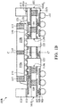
- Fig. 1B is a cross-sectional view of a semiconductor package structure 100b, in accordance with some other embodiments of the disclosure. Descriptions of elements of the embodiments hereinafter that are the same as or similar to those previously described with reference to Fig. 1A are omitted for brevity.
- the semiconductor package structure 100b includes a stress buffer layer 125 filled in the first hole 110a and the second hole 110b.
- the stress buffer layer 125 is made of a polymer material, such as a silicone resin or rubber.
- the stress buffer layer 125 is made of an organic resin, such as Ajinomoto Build-up Film (ABF).
- the stress buffer layer 125 may be formed by a spin coating process. In some other embodiments, a material of the stress buffer layer 125 may be dispensed in the first hole 110a and the second hole 110b, and an excess portion of the material of the stress buffer layer 125 may be removed. In some embodiments, the stress buffer layer 125 may be formed before bonding the first semiconductor die 115a and the second semiconductor die 115b to the substrate 101.
- the stress buffer layer 125 may filled up the first hole 110a and the second hole 110b, and the surfaces of the stress buffer layer 125 are level with the second surface 101b of the substrate 101. In some other embodiments, the surfaces of the stress buffer layer 125 may not be level with the second surface 101b of the substrate 101 according to the actual manufacturing processes.
- Filling the first hole 110a and the second hole 110b with the stress buffer layer 125 may offer advantages like preventing the impurities and dusts from dropping into the first hole 110a and the second hole 110b during the handling process of the substrate 101.
- the warping or cracking problems caused by mismatched coefficients of thermal expansion in the semiconductor package structure 100b can be solved by the holes (including the first hole 110a and the second hole 110b) and the stress buffer layer 125 formed in the substrate 101. Accordingly, the electrical connection within the semiconductor package structure 100b may not be damaged, and the lifespan of the semiconductor package structure 100b may be increased.
- Fig. 2A is a plan view showing shapes of holes in a substrate 201A of a semiconductor package structure 200a
- Fig. 2B is a plan view showing shapes of holes in a substrate 201B of a semiconductor package structure 200b, in accordance with some embodiments of the disclosure. Descriptions of elements of the embodiments hereinafter that are the same as or similar to those previously described with reference to Fig. 1C are omitted for brevity.
- the semiconductor package structure 200a has holes A, B, C, D, E, F, G, H, I, J, K and L in the substrate 201A, and the number of holes in the substrate 201A is much more than that in the substrate 101 of the semiconductor package structure 100a.
- the holes A, B, C, D, E and F are covered by the first semiconductor die 115a
- the holes G, H, I, J, K and L are covered by the second semiconductor die 115b.
- the holes A-F are located within the projection of the first semiconductor die 115a on the substrate 201A
- the holes G-L are located within the projection of the second semiconductor die 115b on the substrate 201A.
- the holes A, B and C are arranged in a first array
- the holes D, E and F are arranged in a second array
- the holes G, H and I are arranged in a third array
- the holes J, K and L are arranged in a fourth array.
- the first array, the second array, the third array and the fourth array are parallel to the center line C-C' of the first semiconductor die 115a and the second semiconductor die 115b.
- the substrate 201B in the semiconductor package structure 200b has holes a, b, c, d, e, f, g, h, i, j, k and 1, which are arranged in the same way as the holes A-L of the substrate 201A in the semiconductor package structure 200a.
- the difference between the substrate 201A and the substrate 201B is that the holes a-1 have circular shapes in the plan view.
- the problems of stress concentrated at the corners of the holes A-L can be prevented in the substrate 201B due to the round shapes of the holes a-1. Therefore, the probability that the cracking problem occurs in the substrate 201B of the semiconductor package structure 200b can be more decreased.
- stress buffer layers may be optionally formed in the holes A-L of the semiconductor package structure 200a and in the holes a-1 of the semiconductor package structure 200b. It should be noted that the holes A-L are symmetrically located about the center line C-C' in the plan view of Fig. 2A , and the holes a-1 are symmetrically located about the center line C-C' in the plan view of Fig. 2B . In some other embodiments, the holes A-L are symmetrically located about the center 201C of the substrate 201A in the plan view of Fig. 2A , and the holes a-1 are symmetrically located about the center 201C' of the substrate 201B in the plan view of Fig. 2B .
- Fig. 3A is a plan view showing arrangements of holes in a substrate 301A of a semiconductor package structure 300a
- Fig. 3B is a plan view showing arrangements of holes in a substrate 301B of a semiconductor package structure 300b, in accordance with some embodiments of the disclosure. Descriptions of elements of the embodiments hereinafter that are the same as or similar to those previously described with reference to Fig. 2A are omitted for brevity.
- the semiconductor package structure 300a has holes A, B, C, D, E, and F in the substrate 301A.
- the holes A, B and C are covered by the first semiconductor die 115a, and the holes D, E and F are covered by the second semiconductor die 115b.
- the holes A-C are located within the projection of the first semiconductor die 115a on the substrate 301A, and the holes D-F are located within the projection of the second semiconductor die 115b on the substrate 301A.
- the holes A-F are arranged radially around the center 301C of the substrate 301A. In some other embodiments, the holes A-F are arranged radially around a center, and the center is located between the first semiconductor die 115a and the second semiconductor die 115b.
- the stress in the substrate 301A of the semiconductor package structure 300a can be released more efficiently.
- the number of the holes in the substrate 301A of the semiconductor package structure 300a can be less than the number of the holes in the substrate 201A of the semiconductor package structure 200a.
- the substrate 201A of the semiconductor package structure 200a which has holes A-L arranged parallel to the center line C-C', is more easily to be manufactured than the substrate 301A of the semiconductor package structure 300a, which has holes A-F arranged radially.
- the substrate 301B in the semiconductor package structure 300b has holes a, b, c, d, e, f, g, h, i, j, k, l, m and n arranged staggered in the substrate 301B.
- the holes a-g are covered by the first semiconductor die 115a and staggered disposed along the direction of the center line C-C'
- the holes h-n are covered by the second semiconductor die 115b and staggered disposed along the direction of the center line C-C'.
- the substrate 301B of the semiconductor package structure 300b can combine the above-mentioned benefits of the hole arrangements of the substrate 201A in the semiconductor package structure 200a and the substrate 301A of the semiconductor package structure 300a. Specifically, the holes a-n in the substrate 301B can be manufactured easily, and the stress in the substrate 301B can be released efficiently.
- stress buffer layers may optionally be formed in the holes A-F of the semiconductor package structure 300a and the holes a-n of the semiconductor package structure 300b.
- the holes A-F are symmetrically located about the center line C-C' in the plan view of Fig. 3A
- the holes a-n are symmetrically located about the center line C-C' in the plan view of Fig. 3B .
- the holes A-F are symmetrically located about the center 301C of the substrate 301A in the plan view of Fig. 3A
- the holes a-n are symmetrically located about the center 301C' of the substrate 301B in the plan view of Fig. 3B .
- Fig. 4A is a plan view showing locations of holes in a substrate 401A of a semiconductor package structure 400a
- Fig. 4B is a plan view showing locations of holes in a substrate 401B of a semiconductor package structure 400b, in accordance with some embodiments of the disclosure. Descriptions of elements of the embodiments hereinafter that are the same as or similar to those previously described with reference to Fig. 2A are omitted for brevity.
- the substrate 401A in the semiconductor package structure 400a has holes A, B, C, D, E, F, G, H, I, J, K and L arranged in the same way as the holes A-L of the substrate 201A in the semiconductor package structure 200a shown in Fig. 2A .
- the holes A-L are arranged parallel to the center line C-C' in the substrate 401A.
- the difference between Figs. 2A and 4A is that the holes A-L in the substrate 401A are located closer to the center 401C of the substrate 401A than the holes A-L in the substrate 201A.
- the stress in the substrate 401A of the semiconductor package structure 400a which has holes A-L located closer to the center 401C of the substrate 401A, can be released more efficiently than the semiconductor package structure 200a.
- the substrate 401B in the semiconductor package structure 400b has holes a, b, c, d, e, f, g, h, i and j located along the peripheral edge of the substrate 401B.
- the holes a-j are located far from the center 401C' of the substrate 401B to reserve space in the middle of the substrate 401B for routing.
- the semiconductor substrate 400b of Fig. 4B can provide a better routing capability for the substrate 401B.
- stress buffer layers may optionally be formed in the holes A-L of the semiconductor package structure 400a and the holes a-j of the semiconductor package structure 400b.
- the holes A-L are symmetrically located about the center line C-C' in the plan view of Fig. 4A
- the holes a-j are symmetrically located about the center line C-C' in the plan view of Fig. 4B .
- the holes A-L are symmetrically located about the center 401C of the substrate 401A in the plan view of Fig. 4A
- the holes a-j are symmetrically located about the center 401C' of the substrate 401B in the plan view of Fig. 4B .
- the holes formed in the substrate are designed to release the stress in the substrate, especially the stress concentrated in the region below the interface between two semiconductor dies. Since the semiconductor package structure may be highly stressed due to the different coefficients of thermal expansion (CTEs) of the substrate and the semiconductor dies, the holes formed in the substrate can solve the warping or cracking problems caused by mismatched CTEs. As a result, the electrical connection within the semiconductor package structure may not be damaged, and the reliability and the lifespan of the semiconductor package structure may be increased.
- CTEs coefficients of thermal expansion
- the semiconductor package structures in accordance with some embodiments of the disclosure can be used to form a three-dimensional (3D) package, a 2.5D package, a fan-out package, or another suitable package.
- the arrangements, the shapes, and the locations of the holes in the substrate can be adjusted according to the types of the application.
Landscapes
- Engineering & Computer Science (AREA)
- Microelectronics & Electronic Packaging (AREA)
- Structures Or Materials For Encapsulating Or Coating Semiconductor Devices Or Solid State Devices (AREA)
- Physics & Mathematics (AREA)
- Geometry (AREA)
Abstract
Description
- This application claims the benefit of
U.S. Provisional Application No. 62/470,915 filed on March 14, 2017 - The present invention relates to a semiconductor package structure, and in particular to a semiconductor package structure with holes formed on a top surface of a substrate therein.
- A semiconductor package can not only provide a semiconductor die with protection from environmental contaminants, but it can also provide an electrical connection between the semiconductor die packaged therein and a substrate, such as a printed circuit board (PCB). For instance, a semiconductor die may be enclosed in an encapsulating material, and traces are electrically connected to the semiconductor die and the substrate.
- However, a problem with such a semiconductor package is that it is subject to different temperatures during the packaging process. The semiconductor package may be highly stressed due to the different coefficients of thermal expansion (CTEs) of the various substrate and semiconductor die materials. As a result, the semiconductor package may exhibit warping or cracking so that the electrical connection between the semiconductor die and the substrate may be damaged, and the reliability of the semiconductor package may be decreased.
- This problem is exacerbated in the case of a relatively large package, for example a package of 50 mm × 50 mm or larger. Therefore, a novel semiconductor package structure is desirable.
- Semiconductor package structures are provided. An exemplary embodiment of a semiconductor package structure includes a substrate having a first surface and a second surface opposite thereto. The substrate includes a wiring structure. The semiconductor package structure also includes a first semiconductor die disposed over the first surface of the substrate and electrically coupled to the wiring structure. The semiconductor package structure further includes a second semiconductor die disposed over the first surface of the substrate and electrically coupled to the wiring structure. The first semiconductor die and the second semiconductor die are separated by a molding material. In addition, the semiconductor package structure includes a first hole and a second hole formed on the second surface of the substrate.
- Another exemplary embodiment of a semiconductor package structure includes a substrate having a wiring structure. The semiconductor package structure also includes a first semiconductor die disposed over the substrate and electrically coupled to the wiring structure. The semiconductor package structure further includes a second semiconductor die disposed over the substrate and electrically coupled to the wiring structure. The first semiconductor die and the second semiconductor die are arranged side-by-side. In addition, the semiconductor package structure includes a plurality of holes formed on a surface of the substrate. The holes are located within projections of the first semiconductor die and the second semiconductor die on the substrate.
- Yet another exemplary embodiment of a substrate structure includes a wiring structure disposed in a substrate, wherein the wiring structure is coupled to a plurality of semiconductor dies disposed over the substrate. The substrate structure also includes a plurality of holes formed on a surface of the substrate, wherein the holes are located within projections of the semiconductor die on the substrate.
- A detailed description is given in the following embodiments with reference to the accompanying drawings.
- The present invention can be more fully understood by reading the subsequent detailed description and examples with references made to the accompanying drawings, wherein:
-
Fig. 1A is a cross-sectional view of a semiconductor package structure, in accordance with some embodiments of the disclosure; -
Fig. 1B is a cross-sectional view of a semiconductor package structure, in accordance with some other embodiments of the disclosure; -
Fig. 1C is a plan view of an arrangement of holes in a substrate of the semiconductor package structure shown inFig. 1A, and Fig. 1A is a cross-sectional view of the semiconductor package structure along line I-I' ofFig. 1C ; -
Figs. 2A-2B are plan views showing shapes of holes in substrates of semiconductor package structures, in accordance with some embodiments of the disclosure; -
Figs. 3A-3B are plan views showing arrangements of holes in substrate of semiconductor package structures, in accordance with some embodiments of the disclosure; and -
Figs. 4A-4B are plan views showing locations of holes in substrates of semiconductor package structures, in accordance with some embodiments of the disclosure. - The following description is of the best-contemplated mode of carrying out the invention. This description is made for the purpose of illustrating the general principles of the invention and should not be taken in a limiting sense. The scope of the invention is determined by reference to the appended claims.
- The present invention will be described with respect to particular embodiments and with reference to certain drawings, but the invention is not limited thereto and is only limited by the claims. The drawings described are only schematic and are non-limiting. In the drawings, the size of some of the elements may be exaggerated for illustrative purposes and not drawn to scale. The dimensions and the relative dimensions do not correspond to actual dimensions in the practice of the invention.
-
Fig. 1A is a cross-sectional view of asemiconductor package structure 100a, in accordance with some embodiments of the disclosure.Fig. 1C is a plan view of an arrangement of holes in asubstrate 101 of thesemiconductor package structure 100a shown inFig. 1A, and Fig. 1A is a cross-sectional view of thesemiconductor package structure 100a along line I-I' ofFig.1C . - Additional features can be added to the
semiconductor package structure 100a. Some of the features described below can be replaced or eliminated for different embodiments. To simplify the diagram, only a portion of thesemiconductor package structure 100a is depicted inFigs. 1A and1C . In some embodiments, thesemiconductor package structure 100a may include a wafer-level semiconductor package, for example, a flip-chip semiconductor package. - Referring to
Fig. 1 , thesemiconductor package structure 100a may be mounted on a base (not shown). In some embodiments, thesemiconductor package structure 100a may be a system-on-chip (SOC) package structure. Moreover, the base may include a printed circuit board (PCB) and may be formed of polypropylene (PP). In some embodiments, the base may include a package substrate. Thesemiconductor package structure 100a is mounted on the base by a bonding process. For example, thesemiconductor package structure 100a includesbump structures 111. In some embodiments, thebump structures 111 may be conductive ball structures (such as ball grid array (BGA)), conductive pillar structures, or conductive paste structures that are mounted on and electrically coupled to the base by the bonding process. - In the embodiment, the
semiconductor package structure 100a includes asubstrate 101. Thesubstrate 101 has a wiring structure therein. In some embodiments, the wiring structure in thesubstrate 101 is a fan-out structure, and may include one or moreconductive pads 103,conductive vias 105,conductive layers 107 andconductive pillars 109. In such cases, the wiring structure in thesubstrate 101 may be disposed in one or more intermetal dielectric (IMD) layers. In some embodiments, the IMD layers may be formed of organic materials, which include a polymer base material, non-organic materials, which include silicon nitride (SiNx), silicon oxide (SiOx), grapheme, or the like. For example, the IMD layers are made of a polymer base material. It should be noted that the number and configuration of the IMD layers, theconductive pads 103, theconductive vias 105, theconductive layers 107 and theconductive pillars 109 shown in Figures and only some examples and are not limitations to the present invention. - Moreover, the
semiconductor package structure 100a also includes afirst semiconductor die 115a and asecond semiconductor die 115b bonded onto thesubstrate 101 through a plurality ofconductive structures 119. Thesubstrate 101 has afirst surface 101a and asecond surface 101b opposite thereto, thefirst surface 101a is facing thefirst semiconductor die 115a and thesecond semiconductor die 115b, and thesecond surface 101b is facing the above-mentioned base. Theconductive structures 119 are disposed over thefirst surface 101a and below thefirst semiconductor die 115a and thesecond semiconductor die 115b, and thebump structures 111 are disposed over thesecond surface 101b of thesubstrate 101. - In some embodiments, the
first semiconductor die 115a and thesecond semiconductor die 115b are electrically coupled to thebump structures 111 through theconductive structures 119 and the wiring structure in thesubstrate 101. In addition, theconductive structures 119 may be controlled collapse chip connection (C4) structures. It should be noted that the number of semiconductor dies integrated in thesemiconductor package structure 100a is not limited to that disclosed in the embodiment. - In some embodiments, the
first semiconductor die 115a and thesecond semiconductor die 115b are active devices. For example, thefirst semiconductor die 115a and thesecond semiconductor die 115b may be logic dies including a central processing unit (CPU), a graphics processing unit (GPU), a dynamic random access memory (DRAM) controller or any combination thereof. In some other embodiments, one or more passive devices are also bonded onto thesubstrate 101. - The
first semiconductor die 115a and the second semiconductor dies 115b are arranged side-by-side. In some embodiments, thefirst semiconductor die 115a and the second semiconductor dies 115b are separated by amolding material 117. Themolding material 117 surrounds thefirst semiconductor die 115a and thesecond semiconductor die 115b, and adjoins the sidewalls of thefirst semiconductor die 115a and thesecond semiconductor die 115b. In some embodiments, themolding material 117 includes a nonconductive material such as an epoxy, a resin, a moldable polymer, or another suitable molding material. In some embodiments, themolding material 117 is applied as a substantial liquid, and then is cured through a chemical reaction. In some other embodiments, themolding material 117 is an ultraviolet (UV) or thermally cured polymer applied as a gel or malleable solid, and then is cured through a UV or thermal curing process. Themolding material 117 may be cured with a mold (not shown). - In some embodiments, the surfaces of the
first semiconductor die 115a and the second semiconductor dies 115b facing away from thefirst surface 101a of thesubstrate 101 are exposed by themolding material 117, such that a heat dissipating device (not shown) can directly attached to the surfaces of thefirst semiconductor die 115a and the second semiconductor dies 115b. As a result, the heat-dissipation efficiency of thesemiconductor package structure 100a can be improved, particularly for a large semiconductor package structure, such as 50 mm x 50 mm, which is preferred for high power applications. - The
semiconductor package structure 100a also includes apolymer material 121 disposed under themolding material 117, thefirst semiconductor die 115a and thesecond semiconductor die 115b, and between theconductive structures 119. Thesemiconductor package structure 100a further includes anunderfill layer 123 interposed between thefirst surface 101a of thesubstrate 101 and thepolymer material 121. In some embodiments, thefirst semiconductor die 115a, the second semiconductor dies 115b and themolding material 117 are surrounded by theunderfill layer 123. Thepolymer material 121 and theunderfill layer 123 are disposed to compensate for differing coefficients of thermal expansion (CTEs) between thesubstrate 101, theconductive structures 119, thefirst semiconductor die 115a and the second semiconductor dies 115b. - In addition, the
semiconductor package structure 100a includes aframe 113 attached to thefirst surface 101a of thesubstrate 101 through anadhesive layer 112. Thefirst semiconductor die 115a and thesecond semiconductor die 115b are surrounded by theframe 113 and theadhesive layer 112. In some embodiments, theframe 113 and theadhesive layer 112 are separated from theunderfill layer 121 by a gap. Thesubstrate 101 has afirst edge 101E1 and asecond edge 101E2 opposite thereto. In some embodiments, thefirst edge 101 E1 and thesecond edge 101E2 are coplanar with sidewalls of theframe 113 and theadhesive layer 112. - Still referring to
Fig. 1A , thesubstrate 101 of thesemiconductor package structure 100a includes afirst hole 110a and asecond hole 110b formed on thesecond surface 101b. In some embodiments, at least one of thefirst hole 110a and thesecond hole 110b penetrates through thesubstrate 101 from thefirst surface 101a to thesecond surface 101b. Although thefirst hole 110a and thesecond hole 110b shown inFig. 1A penetrate through thesubstrate 101, in some other embodiments, both thefirst hole 110a and thesecond hole 110b do not penetrate through thesubstrate 101 from thefirst surface 101a to thesecond surface 101b. In some embodiments, thefirst hole 110a is covered by thefirst semiconductor die 115a, and thesecond hole 110b is covered by thesecond semiconductor die 115b. In other words, thefirst hole 110a is located within the projection of thefirst semiconductor die 115a on thesubstrate 101, and thesecond hole 110b is located within the projection of thesecond semiconductor die 115b on thesubstrate 101. - Specifically, the
first semiconductor die 115a and thesecond semiconductor die 115b have a center line C-C' between them. Thefirst hole 110a is disposed closer to the center line C-C' than thefirst edge 101E1 of thesubstrate 101, and thesecond hole 110b is disposed closer to the center line C-C' than thesecond edge 101E2 of thesubstrate 101. Although there are only two holes in thesubstrate 101 shown inFig. 1A , it should be noted that there is no limitation on the number of the holes formed in thesubstrate 101. - In some embodiments, the
first hole 110a and thesecond hole 110b are formed by a laser drilling process or another suitable process. It should be noted that thefirst hole 110a and thesecond hole 110b may be formed by the same forming process for theconductive pillars 109 in the wiring structure of thesubstrate 101. Moreover, thefirst semiconductor die 115a and thesecond semiconductor die 115b are bonded to thesubstrate 101 after forming the holes in thesubstrate 101. Therefore, the damage of thefirst semiconductor die 115a and thesecond semiconductor die 115b can be prevented. - Referring to
Fig. 1C , which is a plan view of an arrangement of holes in asubstrate 101 of thesemiconductor package structure 100a shown inFig. 1A, and Fig. 1A is a cross-sectional view of thesemiconductor package structure 100a along line I-I' ofFig. 1C . It should be noted thatFig. 1C is the plan view from the bottom of thesemiconductor package structure 100a. In other words,Fig. 1C is the plan view from thesecond surface 101b of thesubstrate 101, which thebump structures 111 are disposed on. In particular, thebump structures 111 are omitted for brevity. - As shown in
Fig.1C , thesubstrate 101 includes more than two holes. In particular, thesubstrate 101 further includes athird hole 110c and thefourth hole 110d formed on thesecond surface 101b. Thethird hole 110c is covered by thefirst semiconductor die 115a, and thefourth hole 110d is covered by thesecond semiconductor die 115b. It should be noted that thesubstrate 101 has acenter 101C, and thefirst hole 101a, thesecond hole 101b, thethird hole 110c, and thefourth hole 110d are disposed closer to thecenter 101C than thefirst edge 101E1 and thesecond edge 101E2 of thesubstrate 101. - The holes formed in the
substrate 101, for example, thefirst hole 110a, thesecond hole 110b, thethird hole 110c and thefourth hole 110d, are designed to release the stress in thesubstrate 101, especially the stress concentrated in the region below the interface between two semiconductor dies (i.e. thefirst semiconductor die 115a and thesecond semiconductor die 115b). Since thesemiconductor package structure 100a may be highly stressed due to the different coefficients of thermal expansion (CTEs) of thesubstrate 101 and the semiconductor dies, the holes formed in thesubstrate 101 can solve the warping or cracking problems caused by mismatched CTEs. As a result, the electrical connection within thesemiconductor package structure 100a may not be damaged, and the reliability of thesemiconductor package structure 100a may be increased. -
Fig. 1B is a cross-sectional view of asemiconductor package structure 100b, in accordance with some other embodiments of the disclosure. Descriptions of elements of the embodiments hereinafter that are the same as or similar to those previously described with reference toFig. 1A are omitted for brevity. - As shown in
Fig. 1B , thesemiconductor package structure 100b includes astress buffer layer 125 filled in thefirst hole 110a and thesecond hole 110b. Thestress buffer layer 125 is made of a polymer material, such as a silicone resin or rubber. In some embodiments, thestress buffer layer 125 is made of an organic resin, such as Ajinomoto Build-up Film (ABF). - Moreover, the
stress buffer layer 125 may be formed by a spin coating process. In some other embodiments, a material of thestress buffer layer 125 may be dispensed in thefirst hole 110a and thesecond hole 110b, and an excess portion of the material of thestress buffer layer 125 may be removed. In some embodiments, thestress buffer layer 125 may be formed before bonding thefirst semiconductor die 115a and thesecond semiconductor die 115b to thesubstrate 101. - In some embodiments, the
stress buffer layer 125 may filled up thefirst hole 110a and thesecond hole 110b, and the surfaces of thestress buffer layer 125 are level with thesecond surface 101b of thesubstrate 101. In some other embodiments, the surfaces of thestress buffer layer 125 may not be level with thesecond surface 101b of thesubstrate 101 according to the actual manufacturing processes. - Filling the
first hole 110a and thesecond hole 110b with thestress buffer layer 125 may offer advantages like preventing the impurities and dusts from dropping into thefirst hole 110a and thesecond hole 110b during the handling process of thesubstrate 101. In addition, the warping or cracking problems caused by mismatched coefficients of thermal expansion in thesemiconductor package structure 100b can be solved by the holes (including thefirst hole 110a and thesecond hole 110b) and thestress buffer layer 125 formed in thesubstrate 101. Accordingly, the electrical connection within thesemiconductor package structure 100b may not be damaged, and the lifespan of thesemiconductor package structure 100b may be increased. -
Fig. 2A is a plan view showing shapes of holes in asubstrate 201A of asemiconductor package structure 200a, andFig. 2B is a plan view showing shapes of holes in asubstrate 201B of asemiconductor package structure 200b, in accordance with some embodiments of the disclosure. Descriptions of elements of the embodiments hereinafter that are the same as or similar to those previously described with reference toFig. 1C are omitted for brevity. - Referring to
Fig. 2A , thesemiconductor package structure 200a has holes A, B, C, D, E, F, G, H, I, J, K and L in thesubstrate 201A, and the number of holes in thesubstrate 201A is much more than that in thesubstrate 101 of thesemiconductor package structure 100a. As shown inFig. 2A , the holes A, B, C, D, E and F are covered by thefirst semiconductor die 115a, and the holes G, H, I, J, K and L are covered by thesecond semiconductor die 115b. In other words, the holes A-F are located within the projection of thefirst semiconductor die 115a on thesubstrate 201A, and the holes G-L are located within the projection of thesecond semiconductor die 115b on thesubstrate 201A. - Specifically, the holes A, B and C are arranged in a first array, the holes D, E and F are arranged in a second array, the holes G, H and I are arranged in a third array, and the holes J, K and L are arranged in a fourth array. The first array, the second array, the third array and the fourth array are parallel to the center line C-C' of the
first semiconductor die 115a and thesecond semiconductor die 115b. - Referring to
Fig. 2B , thesubstrate 201B in thesemiconductor package structure 200b has holes a, b, c, d, e, f, g, h, i, j, k and 1, which are arranged in the same way as the holes A-L of thesubstrate 201A in thesemiconductor package structure 200a. The difference between thesubstrate 201A and thesubstrate 201B is that the holes a-1 have circular shapes in the plan view. Compared with the holes A-L in thesubstrate 201A, which have rectangular shapes in the plan view, the problems of stress concentrated at the corners of the holes A-L can be prevented in thesubstrate 201B due to the round shapes of the holes a-1. Therefore, the probability that the cracking problem occurs in thesubstrate 201B of thesemiconductor package structure 200b can be more decreased. - In some embodiments, stress buffer layers may be optionally formed in the holes A-L of the
semiconductor package structure 200a and in the holes a-1 of thesemiconductor package structure 200b. It should be noted that the holes A-L are symmetrically located about the center line C-C' in the plan view ofFig. 2A , and the holes a-1 are symmetrically located about the center line C-C' in the plan view ofFig. 2B . In some other embodiments, the holes A-L are symmetrically located about thecenter 201C of thesubstrate 201A in the plan view ofFig. 2A , and the holes a-1 are symmetrically located about thecenter 201C' of thesubstrate 201B in the plan view ofFig. 2B . -
Fig. 3A is a plan view showing arrangements of holes in asubstrate 301A of asemiconductor package structure 300a, andFig. 3B is a plan view showing arrangements of holes in asubstrate 301B of asemiconductor package structure 300b, in accordance with some embodiments of the disclosure. Descriptions of elements of the embodiments hereinafter that are the same as or similar to those previously described with reference toFig. 2A are omitted for brevity. - Referring to
Fig. 3A , thesemiconductor package structure 300a has holes A, B, C, D, E, and F in thesubstrate 301A. The holes A, B and C are covered by thefirst semiconductor die 115a, and the holes D, E and F are covered by thesecond semiconductor die 115b. In other words, the holes A-C are located within the projection of thefirst semiconductor die 115a on thesubstrate 301A, and the holes D-F are located within the projection of thesecond semiconductor die 115b on thesubstrate 301A. - It should be noted that the holes A-F are arranged radially around the
center 301C of thesubstrate 301A. In some other embodiments, the holes A-F are arranged radially around a center, and the center is located between thefirst semiconductor die 115a and thesecond semiconductor die 115b. - Compared with the
semiconductor substrate 200a ofFig. 2A , the stress in thesubstrate 301A of thesemiconductor package structure 300a, which has holes A-F arranged radially, can be released more efficiently. In other words, in order to obtain the same stress releasing effect as in thesemiconductor package structure 200a, the number of the holes in thesubstrate 301A of thesemiconductor package structure 300a can be less than the number of the holes in thesubstrate 201A of thesemiconductor package structure 200a. However, thesubstrate 201A of thesemiconductor package structure 200a, which has holes A-L arranged parallel to the center line C-C', is more easily to be manufactured than thesubstrate 301A of thesemiconductor package structure 300a, which has holes A-F arranged radially. - Referring to
Fig. 3B , thesubstrate 301B in thesemiconductor package structure 300b has holes a, b, c, d, e, f, g, h, i, j, k, l, m and n arranged staggered in thesubstrate 301B. Specifically, the holes a-g are covered by thefirst semiconductor die 115a and staggered disposed along the direction of the center line C-C', and the holes h-n are covered by thesecond semiconductor die 115b and staggered disposed along the direction of the center line C-C'. - Compared with the
semiconductor package structure 200a inFig. 2A and thesemiconductor package structure 300a inFig. 3A , thesubstrate 301B of thesemiconductor package structure 300b can combine the above-mentioned benefits of the hole arrangements of thesubstrate 201A in thesemiconductor package structure 200a and thesubstrate 301A of thesemiconductor package structure 300a. Specifically, the holes a-n in thesubstrate 301B can be manufactured easily, and the stress in thesubstrate 301B can be released efficiently. - In some embodiments, stress buffer layers may optionally be formed in the holes A-F of the
semiconductor package structure 300a and the holes a-n of thesemiconductor package structure 300b. It should be noted that the holes A-F are symmetrically located about the center line C-C' in the plan view ofFig. 3A , and the holes a-n are symmetrically located about the center line C-C' in the plan view ofFig. 3B . In some other embodiments, the holes A-F are symmetrically located about thecenter 301C of thesubstrate 301A in the plan view ofFig. 3A , and the holes a-n are symmetrically located about thecenter 301C' of thesubstrate 301B in the plan view ofFig. 3B . -
Fig. 4A is a plan view showing locations of holes in asubstrate 401A of asemiconductor package structure 400a, andFig. 4B is a plan view showing locations of holes in asubstrate 401B of asemiconductor package structure 400b, in accordance with some embodiments of the disclosure. Descriptions of elements of the embodiments hereinafter that are the same as or similar to those previously described with reference toFig. 2A are omitted for brevity. - Referring to
Fig. 4A , thesubstrate 401A in thesemiconductor package structure 400a has holes A, B, C, D, E, F, G, H, I, J, K and L arranged in the same way as the holes A-L of thesubstrate 201A in thesemiconductor package structure 200a shown inFig. 2A . The holes A-L are arranged parallel to the center line C-C' in thesubstrate 401A. The difference betweenFigs. 2A and4A is that the holes A-L in thesubstrate 401A are located closer to thecenter 401C of thesubstrate 401A than the holes A-L in thesubstrate 201A. - Since the maximum stress is likely to be concentrated at the
center 401C of thesubstrate 401A, the stress in thesubstrate 401A of thesemiconductor package structure 400a, which has holes A-L located closer to thecenter 401C of thesubstrate 401A, can be released more efficiently than thesemiconductor package structure 200a. - Referring to
Fig. 4B , thesubstrate 401B in thesemiconductor package structure 400b has holes a, b, c, d, e, f, g, h, i and j located along the peripheral edge of thesubstrate 401B. In other words, the holes a-j are located far from thecenter 401C' of thesubstrate 401B to reserve space in the middle of thesubstrate 401B for routing. Compared with thesemiconductor substrate 400a ofFig. 4A , thesemiconductor substrate 400b ofFig. 4B can provide a better routing capability for thesubstrate 401B. - In some embodiments, stress buffer layers may optionally be formed in the holes A-L of the
semiconductor package structure 400a and the holes a-j of thesemiconductor package structure 400b. It should be noted that the holes A-L are symmetrically located about the center line C-C' in the plan view ofFig. 4A , and the holes a-j are symmetrically located about the center line C-C' in the plan view ofFig. 4B . In some other embodiments, the holes A-L are symmetrically located about thecenter 401C of thesubstrate 401A in the plan view ofFig. 4A , and the holes a-j are symmetrically located about thecenter 401C' of thesubstrate 401B in the plan view ofFig. 4B . - According to the foregoing embodiments, the holes formed in the substrate are designed to release the stress in the substrate, especially the stress concentrated in the region below the interface between two semiconductor dies. Since the semiconductor package structure may be highly stressed due to the different coefficients of thermal expansion (CTEs) of the substrate and the semiconductor dies, the holes formed in the substrate can solve the warping or cracking problems caused by mismatched CTEs. As a result, the electrical connection within the semiconductor package structure may not be damaged, and the reliability and the lifespan of the semiconductor package structure may be increased.
- Many variations and/or modifications can be made to embodiments of the disclosure. The semiconductor package structures in accordance with some embodiments of the disclosure can be used to form a three-dimensional (3D) package, a 2.5D package, a fan-out package, or another suitable package. In addition, the arrangements, the shapes, and the locations of the holes in the substrate can be adjusted according to the types of the application.
- While the invention has been described by way of example and in terms of the preferred embodiments, it is to be understood that the invention is not limited to the disclosed embodiments. On the contrary, it is intended to cover various modifications and similar arrangements (as would be apparent to those skilled in the art). Therefore, the scope of the appended claims should be accorded the broadest interpretation so as to encompass all such modifications and similar arrangements.
- Further aspects of the invention are illustrated by the following examples:
- Example 1: A semiconductor package structure, comprising:
- a substrate having a first surface and a second surface opposite thereto, wherein the substrate comprises a wiring structure;
- a first semiconductor die disposed over the first surface of the substrate and electrically coupled to the wiring structure;
- a second semiconductor die disposed over the first surface of the substrate and electrically coupled to the wiring structure, wherein the first semiconductor die and the second semiconductor die are separated by a molding material; and
- a first hole and a second hole formed on the second surface of the substrate.
- Example 2: The semiconductor package structure as disclosed in example 1, wherein the first hole is covered by the first semiconductor die, and the second hole is covered by the second semiconductor die.
- Example 3: The semiconductor package structure as disclosed in example 1 or 2, wherein the first hole and the second hole are disposed closer to a center line between the first semiconductor die and the second semiconductor die than an edge of the substrate.
- Example 4: The semiconductor package structure as disclosed in one of examples 1 to 3, wherein the first hole and the second hole have rectangular shapes or circular shapes from a plan view.
- Example 5: The semiconductor package structure as disclosed in one of examples 1 to 4, further comprising:
- a third hole and a fourth hole formed on the second surface of the substrate, wherein the third hole is covered by the first semiconductor die, and the fourth hole is covered by the second semiconductor die, and
- wherein the first hole, the second hole, the third hole and the fourth hole are arranged radially around a center of the substrate.
- Example 6: The semiconductor package structure as disclosed in one of examples 1 to 4, further comprising:
- a third hole and a fourth hole formed on the second surface of the substrate, wherein the third hole is covered by the first semiconductor die, and the fourth hole is covered by the second semiconductor die, and
- wherein the first hole and the third hole are arranged in a first array, and the second hole and the fourth hole are arranged in a second array, the first array and the second array are parallel to a center line between the first semiconductor die and the second semiconductor die.
- Example 7: The semiconductor package structure as disclosed in example 6, further comprising:
- a fifth hole and a sixth hole formed on the second surface of the substrate, wherein the fifth hole is covered by the first semiconductor die, and the sixth hole is covered by the second semiconductor die, and
- wherein the first hole, the third hole and the fifth hole are staggered along a direction of the center line, and the second hole, the fourth hole and the sixth hole are staggered along the direction of the center line.
- Example 8: The semiconductor package structure as disclosed in one of examples 1 to 7, further comprising;
a plurality of conductive structures disposed over the first surface and below the first semiconductor die and the second semiconductor die; and
a plurality of bump structures disposed over the second surface of the substrate,
wherein the first semiconductor die and the second semiconductor die are electrically coupled to the bump structures through the conductive structures and the wiring structure in the substrate. - Example 9: The semiconductor package structure as disclosed in one of examples 1 to 8, further comprising:
- a frame disposed over the first surface of the substrate, wherein the frame surrounds the first semiconductor die and the second semiconductor die.
- Example 10: The semiconductor package structure as disclosed in one of examples 1 to 9, wherein the molding material further surrounds the first semiconductor die and the second semiconductor die, and surfaces of the first semiconductor die and the second semiconductor die facing away from the substrate are exposed by the molding material.
- Example 11: The semiconductor package structure as disclosed in one of examples 1 to 10, further comprising:
- a stress buffer layer filled into the first hole and the second hole.
- Example 12: A semiconductor package structure, comprising:
- a substrate having a wiring structure;
- a first semiconductor die disposed over the substrate and electrically coupled to the wiring structure;
- a second semiconductor die disposed over the substrate and electrically coupled to the wiring structure, wherein the first semiconductor die and the second semiconductor die are arranged side-by-side; and
- a plurality of holes formed on a surface of the substrate, wherein the holes are located within projections of the first semiconductor die and the second semiconductor die on the substrate.
- Example 13: The semiconductor package structure as disclosed in example 12, wherein the holes have rectangular shapes or circular shapes from a plan view.
- Example 14: The semiconductor package structure as disclosed in example 12 or 13, wherein the holes are arranged in arrays that are parallel to a center line between the first semiconductor die and the second semiconductor die.
- Example 15: The semiconductor package structure as disclosed in one of examples 12 to 14, wherein the holes are arranged radially around a center, and the center is located between the first semiconductor die and the second semiconductor die.
- Example 16: The semiconductor package structure as disclosed in one of examples 12 to 15, wherein the holes are staggered along a direction parallel to a center line between the first semiconductor die and the second semiconductor die.
- Example 17: The semiconductor package structure as disclosed in one of examples 12 to 16, wherein the holes are located close to a center of the substrate.
- Example 18: The semiconductor package structure as disclosed in one of examples 12 to 17, wherein the holes are located along a peripheral edge of the substrate.
- Example 19: The semiconductor package structure as disclosed in one of examples 12 to 18, wherein the holes are symmetrically located about a center line between the first semiconductor die and the second semiconductor die.
- Example 20: The semiconductor package structure as disclosed in one of examples 12 to 19, further comprising:
- a stress buffer layer filled into the holes, wherein the stress buffer layer is made of a polymer material.
- Example 21: A substrate structure, comprising:
- a wiring structure disposed in a substrate, wherein the wiring structure is coupled to a plurality of semiconductor dies disposed over the substrate; and
- a plurality of holes formed on a surface of the substrate, wherein the holes are located within projections of the semiconductor dies on the substrate.
Claims (12)
- A semiconductor package structure, comprising:a substrate having a first surface and a second surface opposite thereto, wherein the substrate comprises a wiring structure;a first semiconductor die disposed over the first surface of the substrate and electrically coupled to the wiring structure;a second semiconductor die disposed over the first surface of the substrate and electrically coupled to the wiring structure, anda first hole and a second hole formed on the second surface of the substrate.
- The semiconductor package structure as claimed in claim 1, wherein the first hole is located within the projection of, and in particular covered by the first semiconductor die, and the second hole is located in the projection of, and in particular covered by the second semiconductor die.
- The semiconductor package structure as claimed in claim 2, wherein said first and second hole are empty, or a stress buffer layer is filled into the first hole and the second hole, to thereby release stress in the substrate caused by different coefficients of thermal expansion of the substrate and the semiconductor die.
- The semiconductor package structure as claimed in one of the preceding claims, wherein the first hole and the second hole are disposed closer to a center line between the first semiconductor die and the second semiconductor die than to an edge of the substrate.
- The semiconductor package structure as claimed in claim one of the preceding claims, wherein the first hole and the second hole have rectangular shapes or circular shapes from a plan view.
- The semiconductor package structure as claimed in one of the preceding claims, further comprising:a third hole and a fourth hole formed on the second surface of the substrate, wherein the third hole is covered by the first semiconductor die, and the fourth hole is covered by the second semiconductor die, andwherein the first hole, the second hole, the third hole and the fourth hole are arranged radially around a center of the substrate.
- The semiconductor package structure as claimed in one of the preceding claims 1 to 5, further comprising:a third hole and a fourth hole formed on the second surface of the substrate, wherein the third hole is covered by the first semiconductor die, and the fourth hole is covered by the second semiconductor die, andwherein the first hole and the third hole are arranged in a first array, and the second hole and the fourth hole are arranged in a second array, the first array and the second array are parallel to a center line between the first semiconductor die and the second semiconductor die.
- The semiconductor package structure as claimed in claim 7, further comprising:a fifth hole and a sixth hole formed on the second surface of the substrate, wherein the fifth hole is covered by the first semiconductor die, and the sixth hole is covered by the second semiconductor die, andwherein the first hole, the third hole and the fifth hole are staggered along a direction of the center line, and the second hole, the fourth hole and the sixth hole are staggered along the direction of the center line.
- The semiconductor package structure as claimed in one of the preceding claims, further comprising;
a plurality of conductive structures disposed over the first surface and below the first semiconductor die and the second semiconductor die; and
a plurality of bump structures disposed over the second surface of the substrate, wherein the first semiconductor die and the second semiconductor die are electrically coupled to the bump structures through the conductive structures and the wiring structure in the substrate. - The semiconductor package structure as claimed in one of the preceding claims, further comprising:a frame disposed over the first surface of the substrate, wherein the frame surrounds the first semiconductor die and the second semiconductor die.
- The semiconductor package structure of one of the preceding claims, wherein the first semiconductor die and the second semiconductor die are separated by a molding material.
- The semiconductor package structure as claimed in claim 11, wherein the molding material further surrounds the first semiconductor die and the second semiconductor die, and surfaces of the first semiconductor die and the second semiconductor die facing away from the substrate are exposed by the molding material.
Applications Claiming Priority (2)
| Application Number | Priority Date | Filing Date | Title |
|---|---|---|---|
| US201762470915P | 2017-03-14 | 2017-03-14 | |
| US15/906,098 US10784211B2 (en) | 2017-03-14 | 2018-02-27 | Semiconductor package structure |
Publications (2)
| Publication Number | Publication Date |
|---|---|
| EP3376535A1 true EP3376535A1 (en) | 2018-09-19 |
| EP3376535B1 EP3376535B1 (en) | 2022-09-07 |
Family
ID=61581072
Family Applications (1)
| Application Number | Title | Priority Date | Filing Date |
|---|---|---|---|
| EP18160366.3A Active EP3376535B1 (en) | 2017-03-14 | 2018-03-07 | Semiconductor package structure |
Country Status (4)
| Country | Link |
|---|---|
| US (4) | US10784211B2 (en) |
| EP (1) | EP3376535B1 (en) |
| CN (1) | CN108630615A (en) |
| TW (1) | TWI662663B (en) |
Cited By (10)
| Publication number | Priority date | Publication date | Assignee | Title |
|---|---|---|---|---|
| EP3671831A1 (en) * | 2018-12-18 | 2020-06-24 | MediaTek Inc | Semiconductor package structure |
| US10784211B2 (en) | 2017-03-14 | 2020-09-22 | Mediatek Inc. | Semiconductor package structure |
| US11171113B2 (en) | 2017-03-14 | 2021-11-09 | Mediatek Inc. | Semiconductor package structure having an annular frame with truncated corners |
| US11264337B2 (en) | 2017-03-14 | 2022-03-01 | Mediatek Inc. | Semiconductor package structure |
| US11362044B2 (en) | 2017-03-14 | 2022-06-14 | Mediatek Inc. | Semiconductor package structure |
| US11387176B2 (en) | 2017-03-14 | 2022-07-12 | Mediatek Inc. | Semiconductor package structure |
| EP4333045A3 (en) * | 2022-08-30 | 2024-03-20 | NXP USA, Inc. | Packaged power amplifier device with air cavity over die |
| US12327805B2 (en) | 2022-08-30 | 2025-06-10 | Nxp Usa, Inc. | Packaged power amplifier device |
| US12424531B2 (en) | 2017-03-14 | 2025-09-23 | Mediatek Inc. | Semiconductor package structure |
| US12512793B2 (en) | 2022-11-14 | 2025-12-30 | Nxp Usa, Inc. | Power amplifier device having vertical die interconnect structure |
Families Citing this family (13)
| Publication number | Priority date | Publication date | Assignee | Title |
|---|---|---|---|---|
| WO2019005021A1 (en) * | 2017-06-27 | 2019-01-03 | Intel Corporation | Microelectronic devices designed with ultra-high-k dielectric capacitors integrated with package substrates |
| US10957672B2 (en) * | 2017-11-13 | 2021-03-23 | Taiwan Semiconductor Manufacturing Company, Ltd. | Package structure and method of manufacturing the same |
| CN111106096B (en) * | 2018-10-26 | 2024-01-05 | 恒劲科技股份有限公司 | Semiconductor packaging structure and manufacturing method |
| TWI680553B (en) * | 2018-10-26 | 2019-12-21 | 英屬開曼群島商鳳凰先驅股份有限公司 | Semiconductor package structure and method of making the same |
| CN111354684A (en) * | 2018-12-21 | 2020-06-30 | 深南电路股份有限公司 | A chip substrate and its manufacturing method, a packaged chip and its packaging method |
| EP4376067A3 (en) * | 2019-03-14 | 2024-09-04 | MediaTek Inc. | Semiconductor package structure |
| CN112103277B (en) * | 2019-06-17 | 2023-09-01 | 联发科技股份有限公司 | Semiconductor Package Structure |
| TWI771610B (en) * | 2019-09-02 | 2022-07-21 | 矽品精密工業股份有限公司 | Electronic package, carrier structure and manufacturing method thereof |
| TWI730891B (en) * | 2019-09-08 | 2021-06-11 | 聯發科技股份有限公司 | A semiconductor package structure |
| US11469152B2 (en) * | 2019-10-14 | 2022-10-11 | Mediatek Inc. | Semiconductor chip package and fabrication method thereof |
| US11570903B2 (en) * | 2019-10-16 | 2023-01-31 | Advanced Micro Devices, Inc. | Process for conformal coating of multi-row surface-mount components in a lidless BGA package and product made thereby |
| TWI756000B (en) * | 2020-12-28 | 2022-02-21 | 欣興電子股份有限公司 | Chip package structure and manufacturing method thereof |
| KR102671347B1 (en) | 2021-03-17 | 2024-06-03 | 오프로세서 인코퍼레이티드 | Optical Device Module Package |
Citations (7)
| Publication number | Priority date | Publication date | Assignee | Title |
|---|---|---|---|---|
| DE19830158A1 (en) * | 1997-09-30 | 1999-04-22 | Siemens Ag | Intermediate carrier substrate with high wiring density for electronic components |
| JP2003017625A (en) * | 2001-06-29 | 2003-01-17 | Sony Corp | Interposer and semiconductor package |
| US20050186769A1 (en) * | 2004-02-24 | 2005-08-25 | Young Dave W. | Hexagonal array structure for ball grid array packages |
| US20080179725A1 (en) * | 2007-01-30 | 2008-07-31 | Phoenix Precision Technology Corporation | Package structure with circuits directly connected to semiconductor chip |
| EP2066160A2 (en) * | 2007-11-29 | 2009-06-03 | Shinko Electric Industries Co., Ltd. | Wiring board and electronic component device |
| DE102013200518A1 (en) * | 2012-01-19 | 2013-07-25 | Denso Corporation | SEMICONDUCTOR PACKAGE |
| US20140070423A1 (en) * | 2012-09-13 | 2014-03-13 | Invensas Corporation | Tunable composite interposer |
Family Cites Families (62)
| Publication number | Priority date | Publication date | Assignee | Title |
|---|---|---|---|---|
| JP3437369B2 (en) | 1996-03-19 | 2003-08-18 | 松下電器産業株式会社 | Chip carrier and semiconductor device using the same |
| US6020221A (en) | 1996-12-12 | 2000-02-01 | Lsi Logic Corporation | Process for manufacturing a semiconductor device having a stiffener member |
| US5949137A (en) | 1997-09-26 | 1999-09-07 | Lsi Logic Corporation | Stiffener ring and heat spreader for use with flip chip packaging assemblies |
| JPH11260953A (en) | 1998-03-09 | 1999-09-24 | Shinko Electric Ind Co Ltd | Semiconductor chip mounting structure |
| US6313521B1 (en) | 1998-11-04 | 2001-11-06 | Nec Corporation | Semiconductor device and method of manufacturing the same |
| JP3459804B2 (en) | 2000-02-28 | 2003-10-27 | Necエレクトロニクス株式会社 | Semiconductor device |
| US6570469B2 (en) | 2000-06-27 | 2003-05-27 | Matsushita Electric Industrial Co., Ltd. | Multilayer ceramic device including two ceramic layers with multilayer circuit patterns that can support semiconductor and saw chips |
| JP4390541B2 (en) | 2003-02-03 | 2009-12-24 | Necエレクトロニクス株式会社 | Semiconductor device and manufacturing method thereof |
| JP2004247464A (en) | 2003-02-13 | 2004-09-02 | Seiko Epson Corp | Semiconductor device and manufacturing method thereof |
| CN101807533B (en) | 2005-06-30 | 2016-03-09 | 费查尔德半导体有限公司 | Semiconductor die package and manufacturing method thereof |
| US7271480B2 (en) | 2005-09-29 | 2007-09-18 | Taiwan Semiconductor Manufacturing Co., Ltd. | Constraint stiffener design |
| JP4714598B2 (en) | 2006-02-22 | 2011-06-29 | 富士通株式会社 | Semiconductor device and manufacturing method thereof |
| US20080054490A1 (en) | 2006-08-31 | 2008-03-06 | Ati Technologies Inc. | Flip-Chip Ball Grid Array Strip and Package |
| US7851906B2 (en) | 2007-03-26 | 2010-12-14 | Endicott Interconnect Technologies, Inc. | Flexible circuit electronic package with standoffs |
| US20080258293A1 (en) | 2007-04-17 | 2008-10-23 | Advanced Chip Engineering Technology Inc. | Semiconductor device package to improve functions of heat sink and ground shield |
| EP1983158A1 (en) | 2007-04-20 | 2008-10-22 | Siemens Aktiengesellschaft | Method of determining maintenance intervals of a turbomachine and control system therefor |
| KR20090097425A (en) | 2008-03-11 | 2009-09-16 | 주식회사 하이닉스반도체 | Method of forming gate insulating film of semiconductor device |
| US8313984B2 (en) | 2008-03-19 | 2012-11-20 | Ati Technologies Ulc | Die substrate with reinforcement structure |
| US8115303B2 (en) | 2008-05-13 | 2012-02-14 | International Business Machines Corporation | Semiconductor package structures having liquid coolers integrated with first level chip package modules |
| US8216887B2 (en) | 2009-05-04 | 2012-07-10 | Advanced Micro Devices, Inc. | Semiconductor chip package with stiffener frame and configured lid |
| US8710629B2 (en) | 2009-12-17 | 2014-04-29 | Qualcomm Incorporated | Apparatus and method for controlling semiconductor die warpage |
| US8247900B2 (en) | 2009-12-29 | 2012-08-21 | Taiwan Semiconductor Manufacturing Company, Ltd. | Flip chip package having enhanced thermal and mechanical performance |
| EP3547380B1 (en) | 2010-02-09 | 2023-12-20 | Nichia Corporation | Light emitting device |
| KR101678539B1 (en) | 2010-07-21 | 2016-11-23 | 삼성전자 주식회사 | Stack package, semiconductor package and method of manufacturing the stack package |
| CN201936868U (en) | 2010-11-19 | 2011-08-17 | 颀邦科技股份有限公司 | Thin thermal flip chip package structure |
| US8976529B2 (en) | 2011-01-14 | 2015-03-10 | Taiwan Semiconductor Manufacturing Company, Ltd. | Lid design for reliability enhancement in flip chip package |
| US20120188721A1 (en) | 2011-01-21 | 2012-07-26 | Nxp B.V. | Non-metal stiffener ring for fcbga |
| US9887144B2 (en) | 2011-09-08 | 2018-02-06 | Taiwan Semiconductor Manufacturing Company, Ltd. | Ring structure for chip packaging |
| CN104471708B (en) | 2012-02-08 | 2017-05-24 | 吉林克斯公司 | Stacked die assembly with multiple interposers |
| JP2013187740A (en) | 2012-03-08 | 2013-09-19 | Renesas Electronics Corp | Semiconductor device |
| WO2013172420A1 (en) | 2012-05-18 | 2013-11-21 | 京セラ株式会社 | Semiconductor-element-accommodating package, semiconductor device and mounting structure |
| FR2992761B1 (en) | 2012-07-02 | 2015-05-29 | Inside Secure | METHOD FOR MANUFACTURING CONTACTLESS MICROCIRCUIT |
| JP5869686B2 (en) * | 2012-09-27 | 2016-02-24 | 株式会社フジクラ | Optical module |
| US9312193B2 (en) | 2012-11-09 | 2016-04-12 | Taiwan Semiconductor Manufacturing Company, Ltd. | Stress relief structures in package assemblies |
| CN203192781U (en) | 2012-12-13 | 2013-09-11 | 日月光半导体(上海)有限公司 | A packaging substrate strip structure |
| CN103066029B (en) | 2012-12-13 | 2015-07-15 | 日月光半导体(上海)有限公司 | Packaging substrate strip structure and manufacturing method thereof |
| CN203659838U (en) | 2013-10-31 | 2014-06-18 | 中国科学院微电子研究所 | A heat dissipation structure for PoP packaging |
| US9209048B2 (en) | 2013-12-30 | 2015-12-08 | Taiwan Semiconductor Manufacturing Company, Ltd. | Two step molding grinding for packaging applications |
| TWI518854B (en) | 2013-12-30 | 2016-01-21 | 財團法人工業技術研究院 | Molding assembly and molding material |
| US9412662B2 (en) | 2014-01-28 | 2016-08-09 | Taiwan Semiconductor Manufacturing Company, Ltd. | Structure and approach to prevent thin wafer crack |
| KR101676916B1 (en) | 2014-08-20 | 2016-11-16 | 앰코 테크놀로지 코리아 주식회사 | Manufacturing method of semiconductor device amd semiconductor device thereof |
| CN104409366A (en) | 2014-11-19 | 2015-03-11 | 三星半导体(中国)研究开发有限公司 | Chip encapsulating method and encapsulating substrate |
| KR102065943B1 (en) | 2015-04-17 | 2020-01-14 | 삼성전자주식회사 | Fan-out semiconductor package and method of manufacturing the same |
| US9892935B2 (en) | 2015-05-28 | 2018-02-13 | International Business Machines Corporation | Limiting electronic package warpage with semiconductor chip lid and lid-ring |
| US9478504B1 (en) | 2015-06-19 | 2016-10-25 | Invensas Corporation | Microelectronic assemblies with cavities, and methods of fabrication |
| US9425171B1 (en) | 2015-06-25 | 2016-08-23 | Nvidia Corporation | Removable substrate for controlling warpage of an integrated circuit package |
| WO2017029822A1 (en) * | 2015-08-18 | 2017-02-23 | 三菱電機株式会社 | Semiconductor device |
| DK3133166T4 (en) | 2015-08-21 | 2023-03-20 | 42 Life Sciences Gmbh & Co Kg | COMPOSITION AND METHOD OF HYBRIDIZATION |
| US9543249B1 (en) | 2015-09-21 | 2017-01-10 | Dyi-chung Hu | Package substrate with lateral communication circuitry |
| US10546835B2 (en) | 2015-12-22 | 2020-01-28 | Intel Corporation | Microelectronic devices designed with efficient partitioning of high frequency communication devices integrated on a package fabric |
| US10211161B2 (en) * | 2016-08-31 | 2019-02-19 | Advanced Semiconductor Engineering, Inc. | Semiconductor package structure having a protection layer |
| KR102666151B1 (en) | 2016-12-16 | 2024-05-17 | 삼성전자주식회사 | Semiconductor package |
| JP2018113414A (en) | 2017-01-13 | 2018-07-19 | 新光電気工業株式会社 | Semiconductor device and method of manufacturing the same |
| US11302592B2 (en) | 2017-03-08 | 2022-04-12 | Mediatek Inc. | Semiconductor package having a stiffener ring |
| US11387176B2 (en) | 2017-03-14 | 2022-07-12 | Mediatek Inc. | Semiconductor package structure |
| US10784211B2 (en) | 2017-03-14 | 2020-09-22 | Mediatek Inc. | Semiconductor package structure |
| US11362044B2 (en) | 2017-03-14 | 2022-06-14 | Mediatek Inc. | Semiconductor package structure |
| US10529645B2 (en) | 2017-06-08 | 2020-01-07 | Xilinx, Inc. | Methods and apparatus for thermal interface material (TIM) bond line thickness (BLT) reduction and TIM adhesion enhancement for efficient thermal management |
| US10643913B2 (en) | 2017-12-06 | 2020-05-05 | Google Llc | Apparatus and mechanisms for reducing warpage and increasing surface mount technology yields in high performance integrated circuit packages |
| TWM563659U (en) | 2018-01-26 | 2018-07-11 | 奕力科技股份有限公司 | Chip on film package structure |
| US10867925B2 (en) | 2018-07-19 | 2020-12-15 | Taiwan Semiconductor Manufacturing Co., Ltd. | Method for forming chip package structure |
| EP4376067A3 (en) | 2019-03-14 | 2024-09-04 | MediaTek Inc. | Semiconductor package structure |
-
2018
- 2018-02-27 US US15/906,098 patent/US10784211B2/en active Active
- 2018-03-07 EP EP18160366.3A patent/EP3376535B1/en active Active
- 2018-03-08 CN CN201810189557.2A patent/CN108630615A/en not_active Withdrawn
- 2018-03-12 TW TW107108274A patent/TWI662663B/en not_active IP Right Cessation
-
2020
- 2020-08-03 US US16/983,182 patent/US11410936B2/en active Active
-
2022
- 2022-07-04 US US17/810,625 patent/US11948895B2/en active Active
-
2024
- 2024-01-04 US US18/403,974 patent/US12525549B2/en active Active
Patent Citations (7)
| Publication number | Priority date | Publication date | Assignee | Title |
|---|---|---|---|---|
| DE19830158A1 (en) * | 1997-09-30 | 1999-04-22 | Siemens Ag | Intermediate carrier substrate with high wiring density for electronic components |
| JP2003017625A (en) * | 2001-06-29 | 2003-01-17 | Sony Corp | Interposer and semiconductor package |
| US20050186769A1 (en) * | 2004-02-24 | 2005-08-25 | Young Dave W. | Hexagonal array structure for ball grid array packages |
| US20080179725A1 (en) * | 2007-01-30 | 2008-07-31 | Phoenix Precision Technology Corporation | Package structure with circuits directly connected to semiconductor chip |
| EP2066160A2 (en) * | 2007-11-29 | 2009-06-03 | Shinko Electric Industries Co., Ltd. | Wiring board and electronic component device |
| DE102013200518A1 (en) * | 2012-01-19 | 2013-07-25 | Denso Corporation | SEMICONDUCTOR PACKAGE |
| US20140070423A1 (en) * | 2012-09-13 | 2014-03-13 | Invensas Corporation | Tunable composite interposer |
Cited By (20)
| Publication number | Priority date | Publication date | Assignee | Title |
|---|---|---|---|---|
| US11942439B2 (en) | 2017-03-14 | 2024-03-26 | Mediatek Inc. | Semiconductor package structure |
| US10784211B2 (en) | 2017-03-14 | 2020-09-22 | Mediatek Inc. | Semiconductor package structure |
| US11171113B2 (en) | 2017-03-14 | 2021-11-09 | Mediatek Inc. | Semiconductor package structure having an annular frame with truncated corners |
| US11264337B2 (en) | 2017-03-14 | 2022-03-01 | Mediatek Inc. | Semiconductor package structure |
| US11362044B2 (en) | 2017-03-14 | 2022-06-14 | Mediatek Inc. | Semiconductor package structure |
| US11387176B2 (en) | 2017-03-14 | 2022-07-12 | Mediatek Inc. | Semiconductor package structure |
| US11410936B2 (en) | 2017-03-14 | 2022-08-09 | Mediatek Inc. | Semiconductor package structure |
| US11646295B2 (en) | 2017-03-14 | 2023-05-09 | Mediatek Inc. | Semiconductor package structure having an annular frame with truncated corners |
| US12525549B2 (en) | 2017-03-14 | 2026-01-13 | Mediatek Inc. | Semiconductor package structure |
| US11862578B2 (en) | 2017-03-14 | 2024-01-02 | Mediatek Inc. | Semiconductor package structure |
| US12002742B2 (en) | 2017-03-14 | 2024-06-04 | Mediatek Inc. | Semiconductor package structure |
| US11948895B2 (en) | 2017-03-14 | 2024-04-02 | Mediatek Inc. | Semiconductor package structure |
| US12424531B2 (en) | 2017-03-14 | 2025-09-23 | Mediatek Inc. | Semiconductor package structure |
| US12142598B2 (en) | 2017-03-14 | 2024-11-12 | Mediatek Inc. | Semiconductor package structure having an annular frame with truncated corners |
| EP4439648A3 (en) * | 2018-12-18 | 2025-01-15 | MediaTek Inc. | Semiconductor package structure |
| EP3671831A1 (en) * | 2018-12-18 | 2020-06-24 | MediaTek Inc | Semiconductor package structure |
| US12328107B2 (en) | 2022-08-30 | 2025-06-10 | Nxp Usa, Inc. | Packaged power amplifier device with air cavity over die |
| US12327805B2 (en) | 2022-08-30 | 2025-06-10 | Nxp Usa, Inc. | Packaged power amplifier device |
| EP4333045A3 (en) * | 2022-08-30 | 2024-03-20 | NXP USA, Inc. | Packaged power amplifier device with air cavity over die |
| US12512793B2 (en) | 2022-11-14 | 2025-12-30 | Nxp Usa, Inc. | Power amplifier device having vertical die interconnect structure |
Also Published As
| Publication number | Publication date |
|---|---|
| US12525549B2 (en) | 2026-01-13 |
| US20220336374A1 (en) | 2022-10-20 |
| US10784211B2 (en) | 2020-09-22 |
| US11410936B2 (en) | 2022-08-09 |
| US11948895B2 (en) | 2024-04-02 |
| US20200365526A1 (en) | 2020-11-19 |
| TW201834164A (en) | 2018-09-16 |
| CN108630615A (en) | 2018-10-09 |
| EP3376535B1 (en) | 2022-09-07 |
| US20240153887A1 (en) | 2024-05-09 |
| TWI662663B (en) | 2019-06-11 |
| US20180269164A1 (en) | 2018-09-20 |
Similar Documents
| Publication | Publication Date | Title |
|---|---|---|
| US11948895B2 (en) | Semiconductor package structure | |
| EP3709344B1 (en) | Semiconductor package structure | |
| US11942439B2 (en) | Semiconductor package structure | |
| EP3754698B1 (en) | Semiconductor package structure | |
| US11862578B2 (en) | Semiconductor package structure | |
| US12002742B2 (en) | Semiconductor package structure | |
| US10515887B2 (en) | Fan-out package structure having stacked carrier substrates and method for forming the same | |
| US12142598B2 (en) | Semiconductor package structure having an annular frame with truncated corners | |
| EP3671831B1 (en) | Semiconductor package structure | |
| EP3624181B1 (en) | Semiconductor package structure having a frame with truncated corners | |
| US12424531B2 (en) | Semiconductor package structure |
Legal Events
| Date | Code | Title | Description |
|---|---|---|---|
| PUAI | Public reference made under article 153(3) epc to a published international application that has entered the european phase |
Free format text: ORIGINAL CODE: 0009012 |
|
| STAA | Information on the status of an ep patent application or granted ep patent |
Free format text: STATUS: THE APPLICATION HAS BEEN PUBLISHED |
|
| AK | Designated contracting states |
Kind code of ref document: A1 Designated state(s): AL AT BE BG CH CY CZ DE DK EE ES FI FR GB GR HR HU IE IS IT LI LT LU LV MC MK MT NL NO PL PT RO RS SE SI SK SM TR |
|
| AX | Request for extension of the european patent |
Extension state: BA ME |
|
| STAA | Information on the status of an ep patent application or granted ep patent |
Free format text: STATUS: REQUEST FOR EXAMINATION WAS MADE |
|
| 17P | Request for examination filed |
Effective date: 20190312 |
|
| RBV | Designated contracting states (corrected) |
Designated state(s): AL AT BE BG CH CY CZ DE DK EE ES FI FR GB GR HR HU IE IS IT LI LT LU LV MC MK MT NL NO PL PT RO RS SE SI SK SM TR |
|
| STAA | Information on the status of an ep patent application or granted ep patent |
Free format text: STATUS: EXAMINATION IS IN PROGRESS |
|
| 17Q | First examination report despatched |
Effective date: 20201208 |
|
| GRAP | Despatch of communication of intention to grant a patent |
Free format text: ORIGINAL CODE: EPIDOSNIGR1 |
|
| STAA | Information on the status of an ep patent application or granted ep patent |
Free format text: STATUS: GRANT OF PATENT IS INTENDED |
|
| INTG | Intention to grant announced |
Effective date: 20220324 |
|
| GRAS | Grant fee paid |
Free format text: ORIGINAL CODE: EPIDOSNIGR3 |
|
| GRAA | (expected) grant |
Free format text: ORIGINAL CODE: 0009210 |
|
| STAA | Information on the status of an ep patent application or granted ep patent |
Free format text: STATUS: THE PATENT HAS BEEN GRANTED |
|
| AK | Designated contracting states |
Kind code of ref document: B1 Designated state(s): AL AT BE BG CH CY CZ DE DK EE ES FI FR GB GR HR HU IE IS IT LI LT LU LV MC MK MT NL NO PL PT RO RS SE SI SK SM TR |
|
| REG | Reference to a national code |
Ref country code: GB Ref legal event code: FG4D |
|
| REG | Reference to a national code |
Ref country code: CH Ref legal event code: EP Ref country code: AT Ref legal event code: REF Ref document number: 1517768 Country of ref document: AT Kind code of ref document: T Effective date: 20220915 |
|
| REG | Reference to a national code |
Ref country code: IE Ref legal event code: FG4D |
|
| REG | Reference to a national code |
Ref country code: DE Ref legal event code: R096 Ref document number: 602018040221 Country of ref document: DE |
|
| REG | Reference to a national code |
Ref country code: LT Ref legal event code: MG9D |
|
| REG | Reference to a national code |
Ref country code: NL Ref legal event code: MP Effective date: 20220907 |
|
| PG25 | Lapsed in a contracting state [announced via postgrant information from national office to epo] |
Ref country code: SE Free format text: LAPSE BECAUSE OF FAILURE TO SUBMIT A TRANSLATION OF THE DESCRIPTION OR TO PAY THE FEE WITHIN THE PRESCRIBED TIME-LIMIT Effective date: 20220907 Ref country code: RS Free format text: LAPSE BECAUSE OF FAILURE TO SUBMIT A TRANSLATION OF THE DESCRIPTION OR TO PAY THE FEE WITHIN THE PRESCRIBED TIME-LIMIT Effective date: 20220907 Ref country code: NO Free format text: LAPSE BECAUSE OF FAILURE TO SUBMIT A TRANSLATION OF THE DESCRIPTION OR TO PAY THE FEE WITHIN THE PRESCRIBED TIME-LIMIT Effective date: 20221207 Ref country code: LV Free format text: LAPSE BECAUSE OF FAILURE TO SUBMIT A TRANSLATION OF THE DESCRIPTION OR TO PAY THE FEE WITHIN THE PRESCRIBED TIME-LIMIT Effective date: 20220907 Ref country code: LT Free format text: LAPSE BECAUSE OF FAILURE TO SUBMIT A TRANSLATION OF THE DESCRIPTION OR TO PAY THE FEE WITHIN THE PRESCRIBED TIME-LIMIT Effective date: 20220907 Ref country code: FI Free format text: LAPSE BECAUSE OF FAILURE TO SUBMIT A TRANSLATION OF THE DESCRIPTION OR TO PAY THE FEE WITHIN THE PRESCRIBED TIME-LIMIT Effective date: 20220907 |
|
| REG | Reference to a national code |
Ref country code: AT Ref legal event code: MK05 Ref document number: 1517768 Country of ref document: AT Kind code of ref document: T Effective date: 20220907 |
|
| PG25 | Lapsed in a contracting state [announced via postgrant information from national office to epo] |
Ref country code: HR Free format text: LAPSE BECAUSE OF FAILURE TO SUBMIT A TRANSLATION OF THE DESCRIPTION OR TO PAY THE FEE WITHIN THE PRESCRIBED TIME-LIMIT Effective date: 20220907 Ref country code: GR Free format text: LAPSE BECAUSE OF FAILURE TO SUBMIT A TRANSLATION OF THE DESCRIPTION OR TO PAY THE FEE WITHIN THE PRESCRIBED TIME-LIMIT Effective date: 20221208 |
|
| PG25 | Lapsed in a contracting state [announced via postgrant information from national office to epo] |
Ref country code: SM Free format text: LAPSE BECAUSE OF FAILURE TO SUBMIT A TRANSLATION OF THE DESCRIPTION OR TO PAY THE FEE WITHIN THE PRESCRIBED TIME-LIMIT Effective date: 20220907 Ref country code: RO Free format text: LAPSE BECAUSE OF FAILURE TO SUBMIT A TRANSLATION OF THE DESCRIPTION OR TO PAY THE FEE WITHIN THE PRESCRIBED TIME-LIMIT Effective date: 20220907 Ref country code: PT Free format text: LAPSE BECAUSE OF FAILURE TO SUBMIT A TRANSLATION OF THE DESCRIPTION OR TO PAY THE FEE WITHIN THE PRESCRIBED TIME-LIMIT Effective date: 20230109 Ref country code: ES Free format text: LAPSE BECAUSE OF FAILURE TO SUBMIT A TRANSLATION OF THE DESCRIPTION OR TO PAY THE FEE WITHIN THE PRESCRIBED TIME-LIMIT Effective date: 20220907 Ref country code: CZ Free format text: LAPSE BECAUSE OF FAILURE TO SUBMIT A TRANSLATION OF THE DESCRIPTION OR TO PAY THE FEE WITHIN THE PRESCRIBED TIME-LIMIT Effective date: 20220907 Ref country code: AT Free format text: LAPSE BECAUSE OF FAILURE TO SUBMIT A TRANSLATION OF THE DESCRIPTION OR TO PAY THE FEE WITHIN THE PRESCRIBED TIME-LIMIT Effective date: 20220907 |
|
| PG25 | Lapsed in a contracting state [announced via postgrant information from national office to epo] |
Ref country code: SK Free format text: LAPSE BECAUSE OF FAILURE TO SUBMIT A TRANSLATION OF THE DESCRIPTION OR TO PAY THE FEE WITHIN THE PRESCRIBED TIME-LIMIT Effective date: 20220907 Ref country code: PL Free format text: LAPSE BECAUSE OF FAILURE TO SUBMIT A TRANSLATION OF THE DESCRIPTION OR TO PAY THE FEE WITHIN THE PRESCRIBED TIME-LIMIT Effective date: 20220907 Ref country code: IS Free format text: LAPSE BECAUSE OF FAILURE TO SUBMIT A TRANSLATION OF THE DESCRIPTION OR TO PAY THE FEE WITHIN THE PRESCRIBED TIME-LIMIT Effective date: 20230107 Ref country code: EE Free format text: LAPSE BECAUSE OF FAILURE TO SUBMIT A TRANSLATION OF THE DESCRIPTION OR TO PAY THE FEE WITHIN THE PRESCRIBED TIME-LIMIT Effective date: 20220907 |
|
| REG | Reference to a national code |
Ref country code: DE Ref legal event code: R097 Ref document number: 602018040221 Country of ref document: DE |
|
| PG25 | Lapsed in a contracting state [announced via postgrant information from national office to epo] |
Ref country code: NL Free format text: LAPSE BECAUSE OF FAILURE TO SUBMIT A TRANSLATION OF THE DESCRIPTION OR TO PAY THE FEE WITHIN THE PRESCRIBED TIME-LIMIT Effective date: 20220907 Ref country code: AL Free format text: LAPSE BECAUSE OF FAILURE TO SUBMIT A TRANSLATION OF THE DESCRIPTION OR TO PAY THE FEE WITHIN THE PRESCRIBED TIME-LIMIT Effective date: 20220907 |
|
| P01 | Opt-out of the competence of the unified patent court (upc) registered |
Effective date: 20230607 |
|
| PLBE | No opposition filed within time limit |
Free format text: ORIGINAL CODE: 0009261 |
|
| STAA | Information on the status of an ep patent application or granted ep patent |
Free format text: STATUS: NO OPPOSITION FILED WITHIN TIME LIMIT |
|
| PG25 | Lapsed in a contracting state [announced via postgrant information from national office to epo] |
Ref country code: DK Free format text: LAPSE BECAUSE OF FAILURE TO SUBMIT A TRANSLATION OF THE DESCRIPTION OR TO PAY THE FEE WITHIN THE PRESCRIBED TIME-LIMIT Effective date: 20220907 |
|
| 26N | No opposition filed |
Effective date: 20230608 |
|
| PG25 | Lapsed in a contracting state [announced via postgrant information from national office to epo] |
Ref country code: SI Free format text: LAPSE BECAUSE OF FAILURE TO SUBMIT A TRANSLATION OF THE DESCRIPTION OR TO PAY THE FEE WITHIN THE PRESCRIBED TIME-LIMIT Effective date: 20220907 |
|
| PG25 | Lapsed in a contracting state [announced via postgrant information from national office to epo] |
Ref country code: MC Free format text: LAPSE BECAUSE OF FAILURE TO SUBMIT A TRANSLATION OF THE DESCRIPTION OR TO PAY THE FEE WITHIN THE PRESCRIBED TIME-LIMIT Effective date: 20220907 |
|
| REG | Reference to a national code |
Ref country code: CH Ref legal event code: PL |
|
| REG | Reference to a national code |
Ref country code: BE Ref legal event code: MM Effective date: 20230331 |
|
| PG25 | Lapsed in a contracting state [announced via postgrant information from national office to epo] |
Ref country code: LU Free format text: LAPSE BECAUSE OF NON-PAYMENT OF DUE FEES Effective date: 20230307 |
|
| REG | Reference to a national code |
Ref country code: IE Ref legal event code: MM4A |
|
| PG25 | Lapsed in a contracting state [announced via postgrant information from national office to epo] |
Ref country code: LI Free format text: LAPSE BECAUSE OF NON-PAYMENT OF DUE FEES Effective date: 20230331 Ref country code: IE Free format text: LAPSE BECAUSE OF NON-PAYMENT OF DUE FEES Effective date: 20230307 Ref country code: CH Free format text: LAPSE BECAUSE OF NON-PAYMENT OF DUE FEES Effective date: 20230331 |
|
| PG25 | Lapsed in a contracting state [announced via postgrant information from national office to epo] |
Ref country code: BE Free format text: LAPSE BECAUSE OF NON-PAYMENT OF DUE FEES Effective date: 20230331 |
|
| PG25 | Lapsed in a contracting state [announced via postgrant information from national office to epo] |
Ref country code: IT Free format text: LAPSE BECAUSE OF FAILURE TO SUBMIT A TRANSLATION OF THE DESCRIPTION OR TO PAY THE FEE WITHIN THE PRESCRIBED TIME-LIMIT Effective date: 20220907 |
|
| PG25 | Lapsed in a contracting state [announced via postgrant information from national office to epo] |
Ref country code: BG Free format text: LAPSE BECAUSE OF FAILURE TO SUBMIT A TRANSLATION OF THE DESCRIPTION OR TO PAY THE FEE WITHIN THE PRESCRIBED TIME-LIMIT Effective date: 20220907 |
|
| PG25 | Lapsed in a contracting state [announced via postgrant information from national office to epo] |
Ref country code: BG Free format text: LAPSE BECAUSE OF FAILURE TO SUBMIT A TRANSLATION OF THE DESCRIPTION OR TO PAY THE FEE WITHIN THE PRESCRIBED TIME-LIMIT Effective date: 20220907 |
|
| PG25 | Lapsed in a contracting state [announced via postgrant information from national office to epo] |
Ref country code: CY Free format text: LAPSE BECAUSE OF FAILURE TO SUBMIT A TRANSLATION OF THE DESCRIPTION OR TO PAY THE FEE WITHIN THE PRESCRIBED TIME-LIMIT; INVALID AB INITIO Effective date: 20180307 |
|
| PG25 | Lapsed in a contracting state [announced via postgrant information from national office to epo] |
Ref country code: HU Free format text: LAPSE BECAUSE OF FAILURE TO SUBMIT A TRANSLATION OF THE DESCRIPTION OR TO PAY THE FEE WITHIN THE PRESCRIBED TIME-LIMIT; INVALID AB INITIO Effective date: 20180307 |
|
| REG | Reference to a national code |
Ref country code: DE Ref legal event code: R079 Ref document number: 602018040221 Country of ref document: DE Free format text: PREVIOUS MAIN CLASS: H01L0023130000 Ipc: H10W0070680000 |
|
| PG25 | Lapsed in a contracting state [announced via postgrant information from national office to epo] |
Ref country code: TR Free format text: LAPSE BECAUSE OF FAILURE TO SUBMIT A TRANSLATION OF THE DESCRIPTION OR TO PAY THE FEE WITHIN THE PRESCRIBED TIME-LIMIT Effective date: 20220907 |
|
| PGFP | Annual fee paid to national office [announced via postgrant information from national office to epo] |
Ref country code: FR Payment date: 20251231 Year of fee payment: 9 |
|
| PGFP | Annual fee paid to national office [announced via postgrant information from national office to epo] |
Ref country code: GB Payment date: 20260106 Year of fee payment: 9 |
|
| PGFP | Annual fee paid to national office [announced via postgrant information from national office to epo] |
Ref country code: DE Payment date: 20260102 Year of fee payment: 9 |