EP3376542A1 - Solid-state imaging element and method for manufacturing same - Google Patents
Solid-state imaging element and method for manufacturing same Download PDFInfo
- Publication number
- EP3376542A1 EP3376542A1 EP16864390.6A EP16864390A EP3376542A1 EP 3376542 A1 EP3376542 A1 EP 3376542A1 EP 16864390 A EP16864390 A EP 16864390A EP 3376542 A1 EP3376542 A1 EP 3376542A1
- Authority
- EP
- European Patent Office
- Prior art keywords
- microlenses
- solid
- state imaging
- imaging device
- substrate
- Prior art date
- Legal status (The legal status is an assumption and is not a legal conclusion. Google has not performed a legal analysis and makes no representation as to the accuracy of the status listed.)
- Granted
Links
Images





Classifications
-
- G—PHYSICS
- G02—OPTICS
- G02B—OPTICAL ELEMENTS, SYSTEMS OR APPARATUS
- G02B3/00—Simple or compound lenses
-
- H—ELECTRICITY
- H10—SEMICONDUCTOR DEVICES; ELECTRIC SOLID-STATE DEVICES NOT OTHERWISE PROVIDED FOR
- H10F—INORGANIC SEMICONDUCTOR DEVICES SENSITIVE TO INFRARED RADIATION, LIGHT, ELECTROMAGNETIC RADIATION OF SHORTER WAVELENGTH OR CORPUSCULAR RADIATION
- H10F39/00—Integrated devices, or assemblies of multiple devices, comprising at least one element covered by group H10F30/00, e.g. radiation detectors comprising photodiode arrays
- H10F39/80—Constructional details of image sensors
- H10F39/806—Optical elements or arrangements associated with the image sensors
- H10F39/8063—Microlenses
-
- G—PHYSICS
- G02—OPTICS
- G02B—OPTICAL ELEMENTS, SYSTEMS OR APPARATUS
- G02B3/00—Simple or compound lenses
- G02B3/0006—Arrays
- G02B3/0012—Arrays characterised by the manufacturing method
- G02B3/0018—Reflow, i.e. characterized by the step of melting microstructures to form curved surfaces, e.g. manufacturing of moulds and surfaces for transfer etching
-
- H—ELECTRICITY
- H10—SEMICONDUCTOR DEVICES; ELECTRIC SOLID-STATE DEVICES NOT OTHERWISE PROVIDED FOR
- H10F—INORGANIC SEMICONDUCTOR DEVICES SENSITIVE TO INFRARED RADIATION, LIGHT, ELECTROMAGNETIC RADIATION OF SHORTER WAVELENGTH OR CORPUSCULAR RADIATION
- H10F39/00—Integrated devices, or assemblies of multiple devices, comprising at least one element covered by group H10F30/00, e.g. radiation detectors comprising photodiode arrays
- H10F39/011—Manufacture or treatment of image sensors covered by group H10F39/12
- H10F39/024—Manufacture or treatment of image sensors covered by group H10F39/12 of coatings or optical elements
-
- H—ELECTRICITY
- H10—SEMICONDUCTOR DEVICES; ELECTRIC SOLID-STATE DEVICES NOT OTHERWISE PROVIDED FOR
- H10F—INORGANIC SEMICONDUCTOR DEVICES SENSITIVE TO INFRARED RADIATION, LIGHT, ELECTROMAGNETIC RADIATION OF SHORTER WAVELENGTH OR CORPUSCULAR RADIATION
- H10F39/00—Integrated devices, or assemblies of multiple devices, comprising at least one element covered by group H10F30/00, e.g. radiation detectors comprising photodiode arrays
- H10F39/10—Integrated devices
- H10F39/12—Image sensors
- H10F39/18—Complementary metal-oxide-semiconductor [CMOS] image sensors; Photodiode array image sensors
- H10F39/182—Colour image sensors
-
- H—ELECTRICITY
- H10—SEMICONDUCTOR DEVICES; ELECTRIC SOLID-STATE DEVICES NOT OTHERWISE PROVIDED FOR
- H10F—INORGANIC SEMICONDUCTOR DEVICES SENSITIVE TO INFRARED RADIATION, LIGHT, ELECTROMAGNETIC RADIATION OF SHORTER WAVELENGTH OR CORPUSCULAR RADIATION
- H10F39/00—Integrated devices, or assemblies of multiple devices, comprising at least one element covered by group H10F30/00, e.g. radiation detectors comprising photodiode arrays
- H10F39/10—Integrated devices
- H10F39/12—Image sensors
- H10F39/191—Photoconductor image sensors
-
- H—ELECTRICITY
- H10—SEMICONDUCTOR DEVICES; ELECTRIC SOLID-STATE DEVICES NOT OTHERWISE PROVIDED FOR
- H10F—INORGANIC SEMICONDUCTOR DEVICES SENSITIVE TO INFRARED RADIATION, LIGHT, ELECTROMAGNETIC RADIATION OF SHORTER WAVELENGTH OR CORPUSCULAR RADIATION
- H10F39/00—Integrated devices, or assemblies of multiple devices, comprising at least one element covered by group H10F30/00, e.g. radiation detectors comprising photodiode arrays
- H10F39/80—Constructional details of image sensors
- H10F39/805—Coatings
- H10F39/8053—Colour filters
-
- H—ELECTRICITY
- H10—SEMICONDUCTOR DEVICES; ELECTRIC SOLID-STATE DEVICES NOT OTHERWISE PROVIDED FOR
- H10F—INORGANIC SEMICONDUCTOR DEVICES SENSITIVE TO INFRARED RADIATION, LIGHT, ELECTROMAGNETIC RADIATION OF SHORTER WAVELENGTH OR CORPUSCULAR RADIATION
- H10F99/00—Subject matter not provided for in other groups of this subclass
-
- G—PHYSICS
- G02—OPTICS
- G02B—OPTICAL ELEMENTS, SYSTEMS OR APPARATUS
- G02B3/00—Simple or compound lenses
- G02B2003/0093—Simple or compound lenses characterised by the shape
Definitions
- the present invention relates to a solid-state imaging device and a method of manufacturing the same.
- Patent Literatures 1 to 3 Prior arts relating to a solid-state imaging device and a method of manufacturing the same include those described in Patent Literatures 1 to 3.
- a method of manufacturing a solid-state imaging device requires a material constituting the microlens to be patterned a plurality of times. This requires preparation of a plurality of processing jigs such as a patterning mask, which causes a problem of high manufacturing cost.
- the present invention has been made in view of such circumstances, and aims to provide a solid-state imaging device that can be manufactured at lower cost and a method of manufacturing the same.
- the solid-state imaging device is characterized in including a substrate, a plurality of microlenses formed on one surface side of the substrate, and at least one concave lens formed at a boundary between adjacent ones of the plurality of microlenses and depressed toward the one surface of the substrate.
- the method of manufacturing a solid-state imaging device including a substrate, a plurality of microlenses formed on one surface of the substrate, and at least one concave lens formed at a boundary between adjacent ones of the plurality of microlenses and depressed toward the one surface of the substrate, the method being characterized in including the step of collectively forming the microlenses and the concav3e lenses by a photolithography method by use of a gray-tone mask.
- a solid-state imaging device can be produced at low cost.
- FIG. 1 is a cross-sectional view illustrating an exemplary configuration of the solid-state imaging device according to a first embodiment of the present invention. More specifically, FIG. 1(a) is a cross-sectional view illustrating an exemplary configuration of the entire solid-state imaging device according to the first embodiment, and FIG. 1(b) is an enlarged view of an exemplary configuration of the microlens according to the first embodiment.
- a solid-state imaging device 1(1a) includes a semiconductor substrate (substrate) 2 and a lens module 8 formed on one surface (an upper surface in FIG. 1(a) ) side of the semiconductor substrate 2.
- the lens module 8 has a plurality of microlenses 6 and a plurality of concave lenses 7 respectively arranged at a fixed interval in a longitudinal direction and a lateral direction in plan view.
- Each of the plurality of microlenses 6 has a convex shape that protrudes from a surface (the upper surface in FIGs.
- Each of the plurality of concave lenses 7 assumes a concave shape that recesses from the surface of the lens module 8 toward one surface of the semiconductor substrate 2.
- Each of the plurality of concave lenses 7 is located at a boundary between adjacent microlenses 6 of the plurality of microlenses 6.
- a large number of photoelectric transducers are formed on one surface of the semiconductor substrate 2.
- a photodiode is illustrated as a photoelectric transducer.
- a CMOS or CCD is illustrated as a system for transferring photoelectrically converted charges.
- a color separation filter hereinafter also simply referred to as a "color filter”
- a condensing microlens 6 are formed on one surface of the semiconductor substrate 2. The large number of photoelectric transducers are covered by the color filter 5 and the condensing microlens 6.
- one colored layer (a layer colored in one of the three colors of green (G), blue (B), and red (R)) of the color filter 5 is disposed above one photoelectric transducer, and one microlens 6 is disposed thereabove. This combination forms one pixel.
- FIG. 1(a) shows the color filter 5 and omits the photoelectric transducer underneath
- the solid-state imaging device 1a in the present specification includes the semiconductor substrate 2, the plurality of photoelectric transducers, the color filter 5, and the lens module 8.
- a through-hole is provided in the semiconductor substrate 2, the through-hole extending from one surface thereof to another surface (the lower surface in FIG. 1(a) ). Filling the through-hole with a conductive material or covering an inner wall thereof forms a through-hole electrode 9. On another surface of the semiconductor substrate 2, a BGA type connection bump 10 is formed.
- connection bump 10 is also referred to as an external connection pad.
- a single through-hole electrode 9 is electrically connected to a single connection bump 10.
- An electrical signal of an image information captured by the solid-state imaging device 1a passes through an electrode (not shown) formed on the one surface of the semiconductor substrate 2 and the through-hole electrode 9 to be guided to a rear surface of the semiconductor substrate 2 before being output to an external circuit or the like via the connection bump 10.
- a light-shielding electroless plating layer for preventing flare may be applied on a side wall of the lens module 8.
- the light-shielding electroless plating layer include a single plating layer of metal selected from nickel, chromium, cobalt, iron, copper, gold and others and an electroless plating layer of an alloy selected from combinations of nickel-iron, cobalt-iron, copper-iron, etc.
- a metal light-shielding layer having a low optical reflectance on the surface is also possible, the layer being produced by electrolessly depositing copper and other metal, followed by applying a chemical treatment or an oxidation treatment to its surface, to form a metal compound.
- a plurality of microlenses 6 and a plurality of concave lenses 7 are collectively formed by a photolithography method by use of a gray-tone mask 50, which will be described later. This point will be described in detail as an example in the present specification.
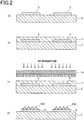
- FIGs. 2(a) to 3(d) are cross-sectional views illustrating a method of manufacturing the solid-state imaging device 1a according to Example 1-1 of the present invention in the order of the manufacturing process.
- a silicon wafer 2' having a 0.75-mm thickness and a 20-cm diameter was prepared as shown in FIG. 2(a) .
- the silicon wafer 2' was a pre-separated silicon substrate.
- a photoelectric transducer, a light-shielding film, and a passivation film were formed on one surface (the upper surface in FIGs. 2 and 3 ) of the silicon wafer 2' and a flattening layer is form on a top layer by spin-coating a thermosetting acrylic resin coating solution.
- G, B, and R color filters 5 were subsequently formed on the flattening layer, each of which was formed by carrying out a photolithography method. Note that illustration of the photoelectric transducer and the flattening layer is omitted in FIG. 2(a) .
- Colorant used for a green resist was, for example, C.I. Pigment Yellow 139, C.I. Pigment Green 36, and C.I. Pigment Blue 15:6. Furthermore, a color resist to which an organic solvent such as cyclohexanone and PGMEA, a polymer varnish, a monomer, and an initiator were added was also used.
- Colorant used for a blue resist was, for example, C.I. Pigment Blue 15:6 and C.I. Pigment Violet 23. Furthermore, a color resist to which an organic solvent such as cyclohexanone and PGMEA, a polymer varnish, a monomer, and an initiator were added was also used.
- Colorant used for a red resist was C.I. Pigment Red 117, C.I. Pigment Red 48:1, and C.I. Pigment Yellow 139.
- a composition other than the colorant was similar to that of the green resist.
- the arrangement of colored pixels was a so-called Bayer arrangement, an arrangement in which a G (green) filter was provided at every other pixel and an R (red) filter and a B (blue) filter were provided on every other line between the G filters.
- a photosensitive microlens material 11 was then formed on the one surface of the silicon wafer 2' to cover the color filters 5.
- the photosensitive microlens material 11 was formed on the color filter 5 by application of a 1- ⁇ m thin styrene resin that was alkali-soluble, photosensitive, and thermally reflowable.
- Example 1-1 is an example in which the lens module 8 shown in FIGs. 1(a) and 1(b) consists of photosensitive microlens material 11.
- the photosensitive microlens material 11 was a photosensitive transparent resin of a positive type.
- the photosensitive microlens material 11 was then exposed to light as shown in FIG. 2(c) .
- a gray-tone mask 50 a special exposure mask, was used here because a convex shape of the microlens 6 and a concave shape of a concave lens 7 were controlled by an exposure method.
- the photosensitive microlens material 11 was heat-treated at 250°C to form the microlenses 6 after being patterned through an ultraviolet-ray (i-ray) photolithographing process by use of the gray-tone mask 50.
- the microlens 6 assumed a gentle semi-parabolic shape that was approximately 0.6 ⁇ m thick.
- the concave lens 7 that was present between adjacent microlenses 6 had a 0.3- ⁇ m concave curvature diameter d (see FIG. 1(b) ).
- the gray-tone mask 50 is a light-shielding film formed on a quartz substrate, the light-shielding film having high transmittance in a part corresponding to a thin part of a lens element to be formed. That is, a mask with a gradation of shades on the light-shielding film was used. The shading of this gradation is achieved by a partial difference of a number of small diameter dots per unit area (density), dots that are not resolved by exposure light.
- the solid-state imaging device 1a multi-layered on a silicon wafer 2' as shown in FIG. 2(d) was prepared.
- a photoresist was then applied onto a rear surface of the silicon wafer 2' described above to form an opening at a site where the through-hole electrode 9 should be formed by a standard photolithography method.
- the silicon wafer 2' was reactive-ion-etched to a predetermined depth by use of the photoresist film as a mask to form a through-hole.
- An SiO 2 -insulating film was then formed on an inner wall, a bottom, and a whole rear surface of the through-hole by a CVD method to insulate the silicon wafer 2' from a wiring layer that will be formed later.
- the insulating film was formed to be thinner at the bottom of the through-hole (a part on a front surface of the silicon wafer 2' where a pad made of a highly conductive metal such as aluminum was formed) than at a rear surface of the silicon wafer 2'.
- the silicon wafer 2' was then reactive-ion-etched once again to remove the insulating film at the bottom of the through-hole.
- a conductive film was subsequently formed by a sputtering method to bury the through-hole and form the wiring layer on the rear surface of the silicon wafer 2'.
- the through-hole electrode 9 was formed as shown in FIG. 3(a) .
- a cutting groove was then formed from a surface by use of a dicing device with a 450-meshed resin blade along an intermediate part of the solid-state imaging device 1a multi-faced in a matrix form.
- Each solid-state imaging device 1a was thereafter separated to produce a finished product as shown in FIG. 3(d) .
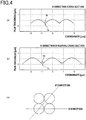
- FIG. 4(a) shows an atomic force microscope (AFM) profile of a cross section in an X direction of the microlens 6 produced in Example 1-1 and an AFM profile of a cross section in an X direction of a conventional microlens, these profiles being overlapped with each other.
- FIG. 4(b) shows an AFM profile of a diagonal cross section in an XY direction of the microlens 6 produced in Example 1-1 and an AFM profile of a diagonal cross section in an XY direction of a conventional microlens, these profiles being overlapped with each other.
- FIG. 4(c) shows a relation between the X direction and the XY direction in a plan view.
- valleys having V-shapes 7a and 7c which are indicated by a solid line, are formed between adjacent microlenses 6.
- concave shapes 7b and 7d are formed between adjacent microlenses 6 in Example 1-1.
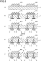
- FIGs. 5(a) to 6(e) are cross-sectional views illustrating a method of manufacturing the solid-state imaging device 1a according to Example 1-2 of the present invention in the order of the manufacturing process.
- a silicon wafer 2' having a 0.75-mm thickness and a 20-cm diameter was prepared as shown in FIG. 5(a) .
- a description on the silicon wafer 2' will be omitted here because it is identical to the silicon wafer 2' described in Example 1-1.
- an acrylic resin liquid was applied on one surface of the silicon wafer 2' to form a 1- ⁇ m thick transparent resin layer 12, before heating the transparent resin layer 12 at 180°C for 3 minutes for hardening, the acrylic resin liquid having a benzene ring that is introduced into a resin skeleton and being applied such that the liquid will cover the color filter 5.
- an alkali-soluble, photosensitive, and thermal reflowable styrene resin was applied on the hardened transparent resin layer 12 to form a photosensitive sacrificial layer 13.
- the photosensitive sacrificial layer 13 was then patterned through a photolithographing process by use of a KrF laser that uses the gray-tone mask 50 before being heat-treated at 250°C to form a lens mold 13a at a 0.1 ⁇ m thermally flowed lens pitch by on one side.
- the lens mold 13a was gently semi-parabolic and approximately 0.7 ⁇ m thick.
- a concave lens 7 that was present between adjacent lens molds 13a had a 0.2- ⁇ m concave curvature diameter d.
- the photosensitive sacrificial layer 13 was dry-etched by use of a mixed gas of fluorocarbon gases CF 4 and C 3 F 8 before a pattern of the lens mold 13a was transferred to the transparent resin layer 12, which was made of an acrylic resin, to form a microlens 6.
- the microlens 6 was approximately 0.6 ⁇ m high, being lower than the lens mold 13a.
- the dry etching process was carried out for 5 minutes.
- the microlens 6 was gently semi-parabolic and approximately 0.6 ⁇ m thick.
- the concave lens 7 that was present between adjacent microlenses 6 had a 0.2- ⁇ m concave curvature diameter d (see FIG. 1(b) ).
- using the KrF laser makes it possible to control the concave curvature diameter d in the concave lens 7 (see FIG. 1 ) within a range from 120 nm to 248 nm by virtue of a wavelength limit resolution of the KrF laser.
- the solid-state imaging device 1a multi-layered on the silicon wafer 2' was produced as shown in FIG. 6(a) .
- a through-hole was then formed as in Example 1-1.
- a wiring layer was then formed as in Example 1-1.
- the through-hole electrode 9 shown in FIG. 6(b) was formed.
- Example 1-1 A solder ball was then mounted to remove residual flux as in Example 1-1.
- the solid-state imaging device substrate having the connection bump 10 shown in FIG. 6(c) was produced.
- the solid-state imaging device substrate was then diced along the cutting line shown in FIG. 6(d) as in Example 1-1.
- the solid-state imaging device substrate was thus separated into individual solid-state imaging devices 1a and to produce a finished product shown in FIG. 6(e) , as in Example 1-1.
- solid-state imaging device 1a and the method of manufacturing the same according to the present embodiment As a reference example of the solid-state imaging device 1a and the method of manufacturing the same according to the present embodiment, a brief description will be given below on a solid-state imaging device and a method of manufacturing the same that do not have a technical characteristic possessed by the solid-state imaging device 1a and the method of manufacturing the same according to the present embodiment.
- An electrical signal of image information retrieved by the solid-state imaging device is guided to a rear surface of a silicon wafer by a conductive material that fills a through-hole formed in the silicon wafer or coats an inner wall thereof.
- the electrical signal can be output to, for example, an external circuit board through a ball grid array (BGA) connecting terminal.
- BGA ball grid array
- a camera module is produced through a process of: preparing a silicon wafer having a diameter of 20 to 30 cm, which is prepared through a glass plate formation process, and a glass plate also having a diameter of 20 to 30 cm, which is prepared through a wafer formation process, and then aligning and laminating the wafer and plate until eventually cutting the laminate into individual camera modules through a dicing process.
- the silicon wafer in the camera module measures 3 mm square; hence approximately 3500 to 4300 camera modules can be formed from a single wafer having a 20-cm diameter.
- inter-lens gap A gap between the adjacent lenses (hereinafter referred to as an "inter-lens gap”) needs to be close to zero to improve condensing efficiency on the solid-state imaging device.
- the inter-lens gap is zero, however, the adjacent microlenses are bonded together, generally making it difficult to control a shape of the inter-lens gap with one nanometer accuracy.
- incident light that enters from the inter-lens gap creates cross-talk between adjacent pixels, which may on occasions deteriorate a condensing efficiency of the microlens.
- Patent Literatures 1 to 3 A proposed solution to these problems is to form a concave lens between adjacent lenses to also collect incident light between the lenses.
- Patent Literatures 1 to 3 contain a description on forming a concave lens between microlenses while forming the microlenses by a thermal flow method or an etching method. These manufacturing methods, however, may on occasions prevent use of a highly heat-resistant microlens material because the material that constitutes the microlens (hereinafter referred to as microlens material) needs to be thermally flowable. In addition, these methods may on occasions increase manufacturing cost due to requirement of a plurality of patterning masks and other processing jigs for patterning on a base material of the microlens several times before thermal flow.
- a solid-state imaging device 1(1b) according to a second embodiment of the present invention is configured almost identically to the solid-state imaging device 1a according to the first embodiment, but is different in having a concave lens 7 whose curvature radius r is 100 nm or less.
- the configuration of the solid-state imaging device 1b according to the present embodiment will be described in detail below.
- the solid-state imaging device 1b includes a semiconductor substrate 2, a plurality of photoelectric transducers 3, a flattening layer 4, a plurality of color filters 5, and a plurality of microlenses 6.
- FIG. 7 is a view taken along the arrow I-I in FIG. 8 .
- FIG. 8 for better understanding of how the plurality of photoelectric transducers 3 (3a to 3i) and the plurality of color filters 5 (5a to 5i) are arranged, other configurations in the solid-state imaging device 1b are omitted. As shown in FIG.
- the solid-state imaging device 1b is formed by a lamination of the plurality of photoelectric transducers 3, the flattening layer 4, the color filter layer constituted by the plurality of color filters 5, and the microlens layer constituted by the plurality of microlenses 6, these components being stacked on the semiconductor substrate 2 in the stated order. Note that this configuration is identical to that of the solid-state imaging device 1 a according to the first embodiment described above.
- the semiconductor substrate 2 is a substrate for mounting the photoelectric transducer 3.
- the plurality of photoelectric transducers 3 convert light incident through the microlens 6 into an electrical charge.
- the plurality of photoelectric transducers 3 are arranged in a two-dimensional square lattice pattern with the plurality of photoelectric transducers 3 being arranged in parallel in a vertical and horizontal direction of FIG. 8 .
- the example shown in FIG. 8 shows a part of the solid-state imaging device lb, where nine photoelectric transducers 3a to 3i are arranged in the square lattice pattern.
- the flattening layer 4 flattens an upper surface (a surface facing upward in FIG. 7 ) of the semiconductor substrate 2, a surface on which the microlenses 6 are mounted.
- the plurality of color filters 5 are respectively formed on the plurality of photoelectric transducers 3 via the flattening layer 4.
- the plurality of color filters 5 act to transmit light of a particular wavelength in light incident on the photoelectric transducer 3.
- the plurality of color filters 5 are arranged in the two-dimensional square lattice pattern on the semiconductor substrate 2 because they are formed corresponding to the plurality of photoelectric transducers 3 arranged in the two-dimensional square lattice pattern in a ratio of 1:1.
- the plurality of color filters 5 in the present embodiment are color filters that transmit one of three colors red (R), green (G), and blue (B), and where these colors are Bayer-arranged. For example, in the example shown in FIG.
- the color filters 5a to 5i are respectively provided in correspondence with the nine photoelectric transducers 3a to 3i.
- the color filters 5a to 5c, 5g and 5h transmit green light
- the color filters 5d and 5e transmit red light
- the color filters 5f and 5i transmit blue light.
- the plurality of microlenses 6 are respectively formed on the plurality of color filters 5.
- the plurality of microlenses 6 are each made of a resin that is usually made of, for example, an acrylic resin that is preferably transparent.
- the plurality of microlenses 6 have a parabolic surface in a cross section parallel to a thickness direction of the semiconductor substrate 2 as shown in FIG. 7 , but may have an arc-like or sinusoidal surface.
- the plurality of microfilters 6 are arranged in the two-dimensional square lattice pattern on the semiconductor substrate 2 because they are formed corresponding to the plurality of color filters 5 arranged in the two-dimensional square lattice pattern in a ratio of 1:1.
- the plurality of microlenses 6 are connected to each other on lower sides of adjacent ones.
- a valley between the plurality of microlenses 6 in a lateral cross section and a 45-degree cross section has a curvature radius of 100 nm or less.
- the term "lateral cross section” here refers to a cross section in a plane parallel to a direction of the plurality of microlenses 6 arranged in the two-dimensional square lattice pattern (the vertical or horizontal direction in FIG. 8 ) and parallel to a thickness direction of the semiconductor substrate 2 (a direction that is longitudinal relative to the drawing plane of FIG. 8 ), a cross section exemplified in FIG. 7 .
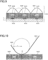
- the 45-degree cross section is a cross section in a plane parallel to a direction inclined by 45 degrees on the semiconductor substrate 2, a direction relative to the arrangement direction of the plurality of microlenses 6, and parallel to the thickness direction of the semiconductor substrate 2, a cross section shown in FIG. 9 , which is a view taken along the arrow II-II of FIG. 8 .
- the curvature radius of the valley between the plurality of microlenses 6 is a curvature radius at the lowermost point, which is the deepest point of the valley between the adjacent microlenses 6.
- the lowermost point of a valley between a microlens 6d and a microlens 6b is indicated by reference numeral 61
- the curvature radius at the lowermost point 61 is indicated by reference character r, as shown in an enlarged view in FIG. 10 .
- the light incident on the microlens 6 in a vicinity of an adjacency above the blue color is influenced by the cross-talk to be redirected to a colored transparent pixel of green (color filter 5b) having a higher refractive index than blue in the color filter layer, for example, as shown in FIG. 11 , which is a view taken along the arrow III-III in FIG. 8 .
- the first step is to sequentially form a flattening layer 4 (not shown in FIG. 13 ) and a color filter layer that is constituted by a plurality of color filters 5 on a semiconductor substrate 2 (not shown in FIG. 13 ) on which a plurality of photoelectric transducers 3 (a filter formation step).
- a filter formation step three types of color filters 5 each corresponding to any one of R, G, and B are arranged and laminated on a plurality of photoelectric transducers 3 to have a predetermined pattern, for example, as shown in FIG. 8 .
- the filter formation step is followed by the step of forming a plurality of microlenses 6 on the plurality of color filters 5 (a lens formation step).
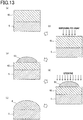
- a photosensitive transparent resin is firstly applied onto a plurality of color filters 5 with a predetermined thickness to form a transparent resin layer 62, as shown in FIG. 13(a) .
- an upper side that serves as a front surface of the transparent resin layer 62 is exposed, developed and baked by a photolithography method by use of a gray-tone mask (not shown in FIG. 13 ) to form a mold 63 for the microlenses 6.
- the mold 63 for the microlens 6 formed on a layer above the transparent resin layer 62 is transferred by a dry-etching transfer method to an identical transparent resin layer 62, as shown in FIGs. 13(d) and 13(e) .
- the mold 63 can be transferred to a layer below the transparent resin layer 62 at an identical etching rate at this time to form a single microlens layer, which makes it possible to faithfully transfer the mold 63 formed on the upper layer.
- adjusting etching conditions particularly a gas type, a gas pressure, a chamber pressure, and an applied voltage, makes it possible to form a microlens 6 with a narrower valley between adjacent microlenses 6.
- Example 2-1 will be described below.
- Example 2-1 a silicon wafer having a 0.75-mm thickness and a 20-cm diameter was used as a semiconductor substrate 2.
- a photoelectric transducer 3 was formed on an upper part of a surface of the silicon wafer, and a flattening layer 4 was formed on an uppermost layer thereof by spin-coating a thermosetting acrylic resin coating solution.
- a color filter layer constituted by tricolored color filters 5 was sequentially formed on the flattening layer 4 by a photolithography method by use of red (R), green (G), and blue (B) color resists.
- Each color filter layer was 0.5 ⁇ m to 0.8 ⁇ m in thickness.
- the pixel arrangement in the color filter layer was a so-called Bayer arrangement, an arrangement in which a G (green) filter are provided at every other pixel and an R (red) filter and a B (blue) filter were provided on every other line between the G filters.
- an alkali-soluble and photosensitive acrylic transparent resin was coated on the color filter layer with a 1.4- ⁇ m thickness before being heated at 180°C for 3 minutes for hardening.
- An acrylic transparent resin layer 62 was thus formed.
- a mold 63 for a microlens 6 was then formed on the acrylic transparent resin layer 62 by a photolithography method by use of a gray-tone mask.
- the gray-tone mask was a light-shielding film formed on a quartz substrate, a light-shielding film that had high transmittance in a part corresponding to a thin part of a microlens element to be formed and that had a gradation of shades. The shading of this gradation is achieved by a partial difference in density per unit area, a partial difference in the number of small diameter dots that are not resolved by exposure light.
- the gray-tone mask used in Example 2-1 is one that was photomasked so that the mold 63 for the microlens 6 may be parabolic. The mold 63 for the microlens 6 was thus parabolic and 0.6 ⁇ m high.
- the mold 63 for the parabolic microlens 6 was then transferred to the acrylic transparent resin layer 62 underneath by the dry-etching transfer method. At this time, the microlens 6 was dry-etched for two minutes by use of a mixed gas of fluorocarbon gases CF 4 and C 3 F 8 and noble gas Ar until it became 0.45 ⁇ m high.
- Example 2-1 Measuring a shape of the microlens 6 formed in Example 2-1 with a scanning probe microscope confirmed that the microlens 6 formed in Example 2-1 was formed to be parabolic, and a curvature radius r of a valley between adjacent microlenses 6 was 50 nm in a cross sectional direction and 24 nm in a 45-degree cross sectional direction.
- Example 2-1 which is a comparison with Example 2-1, a microlens 6 was formed by a photolithography method by use of a gray-tone mask, the microlens 6 being parabolic and a curvature radius r of the valley therebetween being 124 nm in the cross sectional direction and 74 nm in the 45-degree cross sectional direction.
- the "sensitivity" shown in Table 1 is a numerical value in a case where the sensitivity of the conventional solid-state imaging device (Comparative Example 2-1) is assumed to be 100%.
- the sensitivity of the solid-state imaging device 1b formed in Example 2-1, where the conventional solid-state imaging device is made more sensitive is 105.1% as compared with that of the conventional one.
- Example 2-2 will be described below.
- Example 2-2 a photoelectric transducer 3 was formed on an upper surface part of a silicon wafer, and a flattening layer 4 was formed on an uppermost layer thereof, as in Example 2-1.
- a color filter layer constituted by red (R), green (G), and blue (B) color filters 5 was then formed on the flattening layer 4, as also in Example 2-1.
- a mold 63 for a microlens 6 was then formed on the acrylic transparent resin layer 62 by a photolithography method by use of a gray-tone mask.
- the gray-tone mask used in Example 2-2 was one that is photomasked so that the mold 63 for the microlens 6 may be arc-shaped.
- the mold 63 for the microlens 6 was thus arc-shaped and 0.6 ⁇ m high.
- the mold 63 for the arc-shaped microlens 6 was then transferred to the acrylic transparent resin layer 62 underneath by the dry-etching transfer method, as in Example 2-1.
- Example 2-2 Measuring a shape of the microlens 6 formed in Example 2-2 with a scanning probe microscope confirmed that the microlens 6 formed in Example 2-2 was formed to be arc-shaped, and a curvature radius r of a valley between adjacent microlens 6 was 67 nm in a cross sectional direction and 35 nm in a 45-degree cross sectional direction, as shown in Table 2.
- Example 2-2 which was a comparison with Example 2-2, a microlens 6 was formed by a photolithography method by use of a gray-tone mask, the microlens 6 being arc-shaped and a curvature radius r of a valley therebetween being 158 nm in a cross sectional direction and 87 nm in a 45-degree cross sectional direction.
- the "sensitivity" shown in Table 2 is a numerical value in a case where the sensitivity of the conventional solid-state imaging device (Comparative Example 2-2) is assumed to be 100%.
- the sensitivity of the solid-state imaging device 1(b) formed in Example 2-2, where the conventional solid-state imaging device is made more sensitive is 104.7% as compared with that of the conventional one.
- Example 2-3 a photoelectric transducer 3 was formed on an upper surface part of a silicon wafer, and a flattening layer 4 was formed on an uppermost layer thereof, as in Example 2-1.
- a color filter layer constituted by red (R), green (G), and blue (B) color filters 5 was then formed on the flattening layer 4, as also in Example 2-1.
- a mold 63 for a microlens 6 was then formed on the acrylic transparent resin layer 62 by a photolithography method by use of a gray-tone mask.
- the gray-tone mask used in Example 2-3 is one that is photomasked so that the mold 63 for the microlens 6 may be sinusoidal.
- the mold 63 for the microlens 6 was thus sinusoidal and 0.6 ⁇ m high.
- the mold 63 for the sinusoidal microlens 6 was then transferred to the acrylic transparent resin layer 62 underneath by a dry-etching transfer method, as in Example 2-1.
- Example 2-3 Measuring a shape of the microlens 6 formed in Example 2-3 with a scanning probe microscope confirmed that the microlens 6 was formed to be sinusoidal, and a curvature radius r of a valley between adjacent microlens 6 was 89 nm in a cross sectional direction and 56 nm in a 45-degree cross sectional direction, as shown in Table 3.
- Example 2-3 which is a comparison with Example 2-3, a microlens 6 was formed by a photolithography method by use of a gray-tone mask, the microlens 6 being sinusoidal and a curvature radius r of a valley therebetween being 177 nm in a cross sectional direction and 99 nm in a 45-degree cross sectional direction.
- the "sensitivity” shown in Table 3 is a numerical value in a case where the sensitivity of the conventional solid-state imaging device (Comparative Example 2-3) is assumed to be 100%.
- the sensitivity of the solid-state imaging device 1 b formed in Example 2-3, where the conventional solid-state imaging device is made more sensitive is 103.9% as compared with that of the conventional one.
- [Table 3] Microlens shape Curvature radius [nm] Sensitivity Lateral cross section 45-degree cross section Example 2-3 Sinusoidal 89 56 103.9% Comparative Example 2-3 177 99 100.0%
- solid-state imaging device 1b and the method of manufacturing the same according to the present embodiment As a reference example of the solid-state imaging device 1b and the method of manufacturing the same according to the present embodiment, a brief description will be given below of a solid-state imaging device and a method of manufacturing the same that do not have a technical characteristic possessed by the solid-state imaging device 1b and the method of manufacturing the same according to the present embodiment.
- imaging devices have been widely used as more images are recorded and more content is communicated and broadcast.
- various types of imaging devices that have been proposed, an imaging device having a small, lightweight, and sophisticated solid-state imaging device incorporated are becoming common as digital cameras and digital video, solid-state imaging devices being now stably manufactured.
- the solid-state imaging device has a plurality of photoelectric transducers that receive an optical image from an object and convert incident light into an electrical signal.
- the photoelectric transducers are roughly classified into a charge coupled device (CCD) type and a complementary metal oxide semiconductor (CMOS) type.
- CMOS complementary metal oxide semiconductor
- the photoelectric transducers are also roughly classified into linear sensors (line sensors) and area sensors (surface sensors) in terms of how the photoelectric transducers are arranged, the former having photoelectric transducers arranged in a row, and the latter having photoelectric transducers arranged two-dimensionally (lengthwise and breadthwise).
- a color solid-state imaging device as a single-plate type color sensor is widely used as well, the color solid-state imaging device being capable of retrieving color information of an object with a color filtering function provided in a path of light incident on the photoelectric transducer, the color filtering function allowing light of a particular wavelength to pass through.
- a single pixel constituted by a particular colored transparent pixel is patterned in correspondence to a single photoelectric transducer and numerous patterned pixels are regularly arranged, which enables the color solid-state imaging device to collect chromatically resolved image information.
- the three-primary color system which consists of red (R), green (G), and blue (B), and the complementary color system, which consists of cyan (C), magenta (M), and yellow (Y), are common as a color of the colored transparent pixel.
- the three-primary color system in particular, is widely used.
- One of the important performance issues required of the solid-state imaging device is to improve the sensitivity to incident light.
- Increasing an amount of information on an image captured by a miniaturized solid-state imaging device requires miniaturization of a photoelectric transducer that serves as a light receiver for higher integration. Integrating photoelectric transducers more highly, however, reduces an area of each photoelectric transducer, which in turn leaves a lower area ratio available as a light receiver, so that a smaller amount of light can be taken in by the light receiver of the photoelectric transducer, resulting in deteriorated effective sensitivity.
- Proposed as a means for preventing such a miniaturized solid-state imaging device from being less sensitive is a technique for forming a microlens of a uniform shape on the photoelectric transducer to efficiently collect light to the light receiver of the photoelectric transducer, the microlens condensing light incident from an object and guiding the light to the light receiver. Condensing light with the microlens and guiding the light to the light receiver of the photoelectric transducer can increase an apparent aperture ratio of the light receiver, and in turn make the solid-state imaging device more sensitive.
- a transparent acrylic photosensitive resin that serves as a material of the microlens is selectively patterned by a photolithography method before the lens is shaped by virtue of thermal reflowability of the material.
- a lens mold is formed on a flattening layer of an acrylic transparent resin that serves as a material of the microlens by use of an alkali-soluble, photosensitive, and thermally flowable resist material by the photolithography method and thermal reflow. The shape of the lens mold is then transferred to an acrylic transparent resin layer by a dry-etching method to shape the lens (for example, JP-2014-174456 A ).
- An amount of light that can be taken into a light receiver of a photoelectric transducer from a microlens varies depending on a type and thickness of a layer disposed below the microlens; hence a solid-state imaging device configuration by use of a single microlens shape may possibly cause the device to be less sensitive.
- a large curvature radius of a valley on a lateral cross section between adjacent microlenses and on a 45-degree cross section may on occasions be significantly influenced by a phenomenon called cross-talk, a phenomenon in which a certain amount of light leaks from the valley between the microlenses to an adjacent color filter layer.
- the cross-talk here is a phenomenon in which light that should originally enter a certain color is affected by a difference in a refractive index of a pigment of each color to enter a next color. Under the influence of the cross-talk, a color with a low refractive index loses light to the next color with a higher refractive index, so that the light receiver receives a smaller amount of light, which may cause lowered sensitivity.
- a large curvature radius of the valley on the lateral cross section between the adjacent microlenses and on the 45-degree cross section produces a difference in the curvature radius of a microlens shape between a cross section and a 45-degree cross section of a substantially rectangular pixel in a plan view, which may cause aberration, possibly resulting in lowered light-condensing efficiency.
- a microlens optimally shaped according to each solid-state imaging device and having a narrowed curvature radius of a valley between microlenses can alleviate the influence of cross-talk, which leads to better sensitivity of the solid-state imaging device.
- microlenses which are both based on thermal reflow, can narrow the curvature radius of the valley between the microlenses, but have difficulty in processing the microlenses to an optimum shape.
Landscapes
- Physics & Mathematics (AREA)
- General Physics & Mathematics (AREA)
- Optics & Photonics (AREA)
- Engineering & Computer Science (AREA)
- Manufacturing & Machinery (AREA)
- Chemical & Material Sciences (AREA)
- Crystallography & Structural Chemistry (AREA)
- Solid State Image Pick-Up Elements (AREA)
- Transforming Light Signals Into Electric Signals (AREA)
- Multimedia (AREA)
- Signal Processing (AREA)
- Electromagnetism (AREA)
- Exposure And Positioning Against Photoresist Photosensitive Materials (AREA)
Abstract
Description
- The present invention relates to a solid-state imaging device and a method of manufacturing the same.
- Prior arts relating to a solid-state imaging device and a method of manufacturing the same include those described in
Patent Literatures 1 to 3. -
- [PTL 1]
JP-2000-260969 A - [PTL 2]
JP-2000-260970 A - [PTL 3]
JP-2006-165162 A - When forming a plurality of microlenses provided in a solid-state imaging device, a method of manufacturing a solid-state imaging device according to the prior art requires a material constituting the microlens to be patterned a plurality of times. This requires preparation of a plurality of processing jigs such as a patterning mask, which causes a problem of high manufacturing cost.
- The present invention has been made in view of such circumstances, and aims to provide a solid-state imaging device that can be manufactured at lower cost and a method of manufacturing the same.
- To solve the above problem, the solid-state imaging device according to one mode of the present invention is characterized in including a substrate, a plurality of microlenses formed on one surface side of the substrate, and at least one concave lens formed at a boundary between adjacent ones of the plurality of microlenses and depressed toward the one surface of the substrate.
- The method of manufacturing a solid-state imaging device according to one mode of the present invention including a substrate, a plurality of microlenses formed on one surface of the substrate, and at least one concave lens formed at a boundary between adjacent ones of the plurality of microlenses and depressed toward the one surface of the substrate, the method being characterized in including the step of collectively forming the microlenses and the concav3e lenses by a photolithography method by use of a gray-tone mask.
- According to one mode of the present invention, a solid-state imaging device can be produced at low cost.
-
-
FIG. 1 is a cross-sectional view illustrating an exemplary configuration of a solid-state imaging device according to a first embodiment of the present invention. -
FIG. 2 is an explanatory view illustrating a method of manufacturing a solid-state imaging device according to Example 1-1 of the present invention. -
FIG. 3 is an explanatory view illustrating a method of manufacturing a solid-state imaging device according to Example 1-1 of the present invention. -
FIG. 4 is a view illustrating atomic force microscope (AFM) profiles of an X-direction cross section and an XY-direction diagonal cross section of a microlens according to Example 1-1 of the present invention. -
FIG. 5 is an explanatory view illustrating a method of manufacturing a solid-state imaging device according to Example 1-2 of the present invention. -
FIG. 6 is an explanatory view illustrating a method of manufacturing a solid-state imaging device according to Example 2-1 of the present invention. -
FIG. 7 is a cross-sectional view illustrating an exemplary configuration of a solid-state imaging device according to a second embodiment of the present invention. -
FIG. 8 is a plan view illustrating an arrangement of color filters and photoelectric transducers in a solid-state imaging device according to the second embodiment of the present invention. -
FIG. 9 is a cross-sectional view illustrating an exemplary configuration of a solid-state imaging device according to the second embodiment of the present invention. -
FIG. 10 is a partially enlarged cross-sectional view ofFIG. 9 . -
FIG. 11 is an explanatory view illustrating an optical path of light incident between microlenses in a circumstance where a curvature radius of a valley is large. -
FIG. 12 is an explanatory view illustrating an optical path of incident light between microlenses in a circumstance where a curvature radius of a valley is small. -
FIG. 13 is an explanatory view illustrating a method for manufacturing the solid-state imaging device according to the second embodiment of the present invention. - Modes (hereinafter referred to as embodiments) for practicing the present invention will be described with reference to the drawings. In the drawings described below, the same reference numerals are given to parts corresponding to each other, omitting description of the duplicate parts as appropriate. Each embodiment of the present invention exemplifies a configuration for embodying the technical idea of the present invention, and is not intended to limit a material, a shape, a structure, an arrangement, a size and others of each part to those set out below. The technical idea of the present invention is subject to various modifications within the technical scope defined by the claims recited in the Claims section.
- Hereinafter described are main components of the solid-state imaging device according to the first embodiment of the present invention. A detailed configuration of the solid-state imaging device will be described in the second embodiment of the present invention described later.
-
FIG. 1 is a cross-sectional view illustrating an exemplary configuration of the solid-state imaging device according to a first embodiment of the present invention. More specifically,FIG. 1(a) is a cross-sectional view illustrating an exemplary configuration of the entire solid-state imaging device according to the first embodiment, andFIG. 1(b) is an enlarged view of an exemplary configuration of the microlens according to the first embodiment. - As shown in
FIG. 1(a) , a solid-state imaging device 1(1a) according to the present embodiment includes a semiconductor substrate (substrate) 2 and alens module 8 formed on one surface (an upper surface inFIG. 1(a) ) side of thesemiconductor substrate 2. As shown inFIGs. 1(a) and 1(b) , thelens module 8 has a plurality ofmicrolenses 6 and a plurality ofconcave lenses 7 respectively arranged at a fixed interval in a longitudinal direction and a lateral direction in plan view. Each of the plurality ofmicrolenses 6 has a convex shape that protrudes from a surface (the upper surface inFIGs. 1(a) and 1(b) ) of the lens module 8 (in other words, it is a convex lens). Each of the plurality ofconcave lenses 7 assumes a concave shape that recesses from the surface of thelens module 8 toward one surface of thesemiconductor substrate 2. Each of the plurality ofconcave lenses 7 is located at a boundary betweenadjacent microlenses 6 of the plurality ofmicrolenses 6. - Although not shown, a large number of photoelectric transducers are formed on one surface of the
semiconductor substrate 2. A photodiode is illustrated as a photoelectric transducer. In addition, a CMOS or CCD is illustrated as a system for transferring photoelectrically converted charges. Further, a color separation filter (hereinafter also simply referred to as a "color filter") 5 and acondensing microlens 6 are formed on one surface of thesemiconductor substrate 2. The large number of photoelectric transducers are covered by thecolor filter 5 and thecondensing microlens 6. For example, one colored layer (a layer colored in one of the three colors of green (G), blue (B), and red (R)) of thecolor filter 5 is disposed above one photoelectric transducer, and onemicrolens 6 is disposed thereabove. This combination forms one pixel. - Although
FIG. 1(a) shows thecolor filter 5 and omits the photoelectric transducer underneath, the solid-state imaging device 1a in the present specification includes thesemiconductor substrate 2, the plurality of photoelectric transducers, thecolor filter 5, and thelens module 8. - As shown in
FIG. 1(a) , a through-hole is provided in thesemiconductor substrate 2, the through-hole extending from one surface thereof to another surface (the lower surface inFIG. 1(a) ). Filling the through-hole with a conductive material or covering an inner wall thereof forms a through-hole electrode 9. On another surface of thesemiconductor substrate 2, a BGAtype connection bump 10 is formed. - The
connection bump 10 is also referred to as an external connection pad. A single through-hole electrode 9 is electrically connected to asingle connection bump 10. - An electrical signal of an image information captured by the solid-
state imaging device 1a passes through an electrode (not shown) formed on the one surface of thesemiconductor substrate 2 and the through-hole electrode 9 to be guided to a rear surface of thesemiconductor substrate 2 before being output to an external circuit or the like via theconnection bump 10. - In the solid-
state imaging device 1a according to the present embodiment, a light-shielding electroless plating layer for preventing flare may be applied on a side wall of thelens module 8. Examples of the light-shielding electroless plating layer include a single plating layer of metal selected from nickel, chromium, cobalt, iron, copper, gold and others and an electroless plating layer of an alloy selected from combinations of nickel-iron, cobalt-iron, copper-iron, etc. In addition, a metal light-shielding layer having a low optical reflectance on the surface is also possible, the layer being produced by electrolessly depositing copper and other metal, followed by applying a chemical treatment or an oxidation treatment to its surface, to form a metal compound. - In the method of manufacturing the solid-
state imaging device 1a according to the present embodiment, a plurality ofmicrolenses 6 and a plurality ofconcave lenses 7 are collectively formed by a photolithography method by use of a gray-tone mask 50, which will be described later. This point will be described in detail as an example in the present specification. -
FIGs. 2(a) to 3(d) are cross-sectional views illustrating a method of manufacturing the solid-state imaging device 1a according to Example 1-1 of the present invention in the order of the manufacturing process. A silicon wafer 2' having a 0.75-mm thickness and a 20-cm diameter was prepared as shown inFIG. 2(a) . The silicon wafer 2' was a pre-separated silicon substrate. A photoelectric transducer, a light-shielding film, and a passivation film were formed on one surface (the upper surface inFIGs. 2 and3 ) of the silicon wafer 2' and a flattening layer is form on a top layer by spin-coating a thermosetting acrylic resin coating solution. G, B, andR color filters 5 were subsequently formed on the flattening layer, each of which was formed by carrying out a photolithography method. Note that illustration of the photoelectric transducer and the flattening layer is omitted inFIG. 2(a) . - Colorant used for a green resist was, for example, C.I. Pigment Yellow 139, C.I. Pigment Green 36, and C.I. Pigment Blue 15:6. Furthermore, a color resist to which an organic solvent such as cyclohexanone and PGMEA, a polymer varnish, a monomer, and an initiator were added was also used.
- Colorant used for a blue resist was, for example, C.I. Pigment Blue 15:6 and C.I. Pigment Violet 23. Furthermore, a color resist to which an organic solvent such as cyclohexanone and PGMEA, a polymer varnish, a monomer, and an initiator were added was also used.
- Colorant used for a red resist was C.I. Pigment Red 117, C.I. Pigment Red 48:1, and C.I. Pigment Yellow 139. A composition other than the colorant was similar to that of the green resist.
- The arrangement of colored pixels was a so-called Bayer arrangement, an arrangement in which a G (green) filter was provided at every other pixel and an R (red) filter and a B (blue) filter were provided on every other line between the G filters.
- As shown in
FIG. 2(b) , aphotosensitive microlens material 11 was then formed on the one surface of the silicon wafer 2' to cover the color filters 5. Here thephotosensitive microlens material 11 was formed on thecolor filter 5 by application of a 1-µm thin styrene resin that was alkali-soluble, photosensitive, and thermally reflowable. Example 1-1 is an example in which thelens module 8 shown inFIGs. 1(a) and 1(b) consists ofphotosensitive microlens material 11. Thephotosensitive microlens material 11 was a photosensitive transparent resin of a positive type. - The
photosensitive microlens material 11 was then exposed to light as shown inFIG. 2(c) . A gray-tone mask 50, a special exposure mask, was used here because a convex shape of themicrolens 6 and a concave shape of aconcave lens 7 were controlled by an exposure method. Specifically, thephotosensitive microlens material 11 was heat-treated at 250°C to form themicrolenses 6 after being patterned through an ultraviolet-ray (i-ray) photolithographing process by use of the gray-tone mask 50. Themicrolens 6 assumed a gentle semi-parabolic shape that was approximately 0.6 µm thick. Theconcave lens 7 that was present betweenadjacent microlenses 6 had a 0.3-µm concave curvature diameter d (seeFIG. 1(b) ). - The gray-
tone mask 50 is a light-shielding film formed on a quartz substrate, the light-shielding film having high transmittance in a part corresponding to a thin part of a lens element to be formed. That is, a mask with a gradation of shades on the light-shielding film was used. The shading of this gradation is achieved by a partial difference of a number of small diameter dots per unit area (density), dots that are not resolved by exposure light. - Thus, the solid-
state imaging device 1a multi-layered on a silicon wafer 2' as shown inFIG. 2(d) was prepared. - A photoresist was then applied onto a rear surface of the silicon wafer 2' described above to form an opening at a site where the through-
hole electrode 9 should be formed by a standard photolithography method. The silicon wafer 2' was reactive-ion-etched to a predetermined depth by use of the photoresist film as a mask to form a through-hole. - An SiO2-insulating film was then formed on an inner wall, a bottom, and a whole rear surface of the through-hole by a CVD method to insulate the silicon wafer 2' from a wiring layer that will be formed later. The insulating film was formed to be thinner at the bottom of the through-hole (a part on a front surface of the silicon wafer 2' where a pad made of a highly conductive metal such as aluminum was formed) than at a rear surface of the silicon wafer 2'. The silicon wafer 2' was then reactive-ion-etched once again to remove the insulating film at the bottom of the through-hole. A conductive film was subsequently formed by a sputtering method to bury the through-hole and form the wiring layer on the rear surface of the silicon wafer 2'. In other words, the through-
hole electrode 9 was formed as shown inFIG. 3(a) . - A part of the wiring layer, a part to be connected to an outside, was then exposed by a standard photolithography method. Solder paste was screen-printed onto the exposed part to mount a solder ball. Removing residual flux through a reflow treatment produced a solid-state imaging device substrate having connection bumps 10, as shown in
FIG. 3(b) . - As shown in
FIG. 3(c) , a cutting groove was then formed from a surface by use of a dicing device with a 450-meshed resin blade along an intermediate part of the solid-state imaging device 1a multi-faced in a matrix form. Each solid-state imaging device 1a was thereafter separated to produce a finished product as shown inFIG. 3(d) . - It is also possible to control a shape and light transmittance of the
microlens 6 by carrying out a bleaching and other step as necessary. -
FIG. 4(a) shows an atomic force microscope (AFM) profile of a cross section in an X direction of themicrolens 6 produced in Example 1-1 and an AFM profile of a cross section in an X direction of a conventional microlens, these profiles being overlapped with each other.FIG. 4(b) shows an AFM profile of a diagonal cross section in an XY direction of themicrolens 6 produced in Example 1-1 and an AFM profile of a diagonal cross section in an XY direction of a conventional microlens, these profiles being overlapped with each other.FIG. 4(c) shows a relation between the X direction and the XY direction in a plan view. For the conventional microlens, valleys having V-shapes adjacent microlenses 6. In contrast,concave shapes adjacent microlenses 6 in Example 1-1. -
FIGs. 5(a) to 6(e) are cross-sectional views illustrating a method of manufacturing the solid-state imaging device 1a according to Example 1-2 of the present invention in the order of the manufacturing process. A silicon wafer 2' having a 0.75-mm thickness and a 20-cm diameter was prepared as shown inFIG. 5(a) . A description on the silicon wafer 2' will be omitted here because it is identical to the silicon wafer 2' described in Example 1-1. - As shown in
FIG. 5(b) , an acrylic resin liquid was applied on one surface of the silicon wafer 2' to form a 1-µm thicktransparent resin layer 12, before heating thetransparent resin layer 12 at 180°C for 3 minutes for hardening, the acrylic resin liquid having a benzene ring that is introduced into a resin skeleton and being applied such that the liquid will cover thecolor filter 5. - In addition, as shown in
FIG. 5(c) , an alkali-soluble, photosensitive, and thermal reflowable styrene resin was applied on the hardenedtransparent resin layer 12 to form a photosensitivesacrificial layer 13. - The photosensitive
sacrificial layer 13 was then patterned through a photolithographing process by use of a KrF laser that uses the gray-tone mask 50 before being heat-treated at 250°C to form alens mold 13a at a 0.1 µm thermally flowed lens pitch by on one side. Thelens mold 13a was gently semi-parabolic and approximately 0.7 µm thick. Aconcave lens 7 that was present betweenadjacent lens molds 13a had a 0.2-µm concave curvature diameter d. - Then, as shown in
FIG. 5(d) , the photosensitivesacrificial layer 13 was dry-etched by use of a mixed gas of fluorocarbon gases CF4 and C3F8 before a pattern of thelens mold 13a was transferred to thetransparent resin layer 12, which was made of an acrylic resin, to form amicrolens 6. Themicrolens 6 was approximately 0.6 µm high, being lower than thelens mold 13a. The dry etching process was carried out for 5 minutes. Themicrolens 6 was gently semi-parabolic and approximately 0.6 µm thick. Theconcave lens 7 that was present betweenadjacent microlenses 6 had a 0.2-µm concave curvature diameter d (seeFIG. 1(b) ). - In the photolithography method using the gray-
tone mask 50, using the KrF laser makes it possible to control the concave curvature diameter d in the concave lens 7 (seeFIG. 1 ) within a range from 120 nm to 248 nm by virtue of a wavelength limit resolution of the KrF laser. - Thus, the solid-
state imaging device 1a multi-layered on the silicon wafer 2' was produced as shown inFIG. 6(a) . - A through-hole was then formed as in Example 1-1.
- A wiring layer was then formed as in Example 1-1. Thus, the through-
hole electrode 9 shown inFIG. 6(b) was formed. - A solder ball was then mounted to remove residual flux as in Example 1-1. Thus, the solid-state imaging device substrate having the
connection bump 10 shown inFIG. 6(c) was produced. - The solid-state imaging device substrate was then diced along the cutting line shown in
FIG. 6(d) as in Example 1-1. The solid-state imaging device substrate was thus separated into individual solid-state imaging devices 1a and to produce a finished product shown inFIG. 6(e) , as in Example 1-1. - It is also possible to control a shape and light transmittance of the
microlens 6 by carrying out a bleaching and other step as necessary. -
- (1) As described above, the present embodiment collectively forms the
microlens 6 and theconcave lens 7 by the photolithography method by use of the gray-tone mask 50. This eliminates the need for a microlens material (e.g., thephotosensitive microlens material 11 and the transparent resin layer 12) to be thermally flowable, and therefore eliminating the need to use a highly heat-resistant microlens material, which makes it possible to lower material cost. This also eliminates the need to pattern the microlens material several times, which in turn enables using fewer processing steps, hence making it possible to form a solid-state imaging device at lower cost. - (2) Additionally, collectively forming the
microlens 6 and theconcave lens 7 by the photolithography method by use of the gray-tone mask 50 prevents themicrolenses 6 from being fused together, which enables effective use of light incident on a boundary (gap region) between theadjacent microlenses 6; hence makes it possible to manufacture a more sensitive solid-state imaging device 1a. This technique is particularly effective for an improvement in light collection efficiency of a high-definition microlens having a lens pitch of 6 microns or less. - (3) Further, a limit resolution of an i-ray, which is ultraviolet light, advantageously facilitates formation of a
concave lens 7 having a concave curvature diameter d of 180 nm through 365 nm or less betweenadjacent microlenses 6. Still further, the limit resolution of the KrF laser advantageously facilitates formation of aconcave lens 7 having a concave curvature diameter d of 120 nm through 248 nm betweenadjacent microlenses 6. - As a reference example of the solid-
state imaging device 1a and the method of manufacturing the same according to the present embodiment, a brief description will be given below on a solid-state imaging device and a method of manufacturing the same that do not have a technical characteristic possessed by the solid-state imaging device 1a and the method of manufacturing the same according to the present embodiment. - In recent years, a module structure that can be manufactured by a wafer process has been proposed for reduction in size and thickness of a camera module (see
Patent Literatures 1 to 3). In each pixel on a photoelectric transducer surface on an upper surface of a silicon wafer on which a solid-state imaging device is formed, a color separation filter and a condensing microlens are formed. - An electrical signal of image information retrieved by the solid-state imaging device is guided to a rear surface of a silicon wafer by a conductive material that fills a through-hole formed in the silicon wafer or coats an inner wall thereof. The electrical signal can be output to, for example, an external circuit board through a ball grid array (BGA) connecting terminal.
- A camera module is produced through a process of: preparing a silicon wafer having a diameter of 20 to 30 cm, which is prepared through a glass plate formation process, and a glass plate also having a diameter of 20 to 30 cm, which is prepared through a wafer formation process, and then aligning and laminating the wafer and plate until eventually cutting the laminate into individual camera modules through a dicing process.
- For a camera generally mounted on a cellular phone, the silicon wafer in the
camera module measures 3 mm square; hence approximately 3500 to 4300 camera modules can be formed from a single wafer having a 20-cm diameter. - A gap between the adjacent lenses (hereinafter referred to as an "inter-lens gap") needs to be close to zero to improve condensing efficiency on the solid-state imaging device. In a circumstance where the inter-lens gap is zero, however, the adjacent microlenses are bonded together, generally making it difficult to control a shape of the inter-lens gap with one nanometer accuracy.
- In a circumstance where an inter-lens gap is provided, incident light that enters from the inter-lens gap creates cross-talk between adjacent pixels, which may on occasions deteriorate a condensing efficiency of the microlens.
- A proposed solution to these problems is to form a concave lens between adjacent lenses to also collect incident light between the lenses (
Patent Literatures 1 to 3). - The
above Patent Literatures 1 to 3 contain a description on forming a concave lens between microlenses while forming the microlenses by a thermal flow method or an etching method. These manufacturing methods, however, may on occasions prevent use of a highly heat-resistant microlens material because the material that constitutes the microlens (hereinafter referred to as microlens material) needs to be thermally flowable. In addition, these methods may on occasions increase manufacturing cost due to requirement of a plurality of patterning masks and other processing jigs for patterning on a base material of the microlens several times before thermal flow. - A solid-state imaging device 1(1b) according to a second embodiment of the present invention is configured almost identically to the solid-
state imaging device 1a according to the first embodiment, but is different in having aconcave lens 7 whose curvature radius r is 100 nm or less. The configuration of the solid-state imaging device 1b according to the present embodiment will be described in detail below. - As shown in
FIGs. 7 and 8 , the solid-state imaging device 1b according to the second embodiment of the present invention includes asemiconductor substrate 2, a plurality ofphotoelectric transducers 3, aflattening layer 4, a plurality ofcolor filters 5, and a plurality ofmicrolenses 6.FIG. 7 is a view taken along the arrow I-I inFIG. 8 . InFIG. 8 , for better understanding of how the plurality of photoelectric transducers 3 (3a to 3i) and the plurality of color filters 5 (5a to 5i) are arranged, other configurations in the solid-state imaging device 1b are omitted. As shown inFIG. 7 , the solid-state imaging device 1b is formed by a lamination of the plurality ofphotoelectric transducers 3, theflattening layer 4, the color filter layer constituted by the plurality ofcolor filters 5, and the microlens layer constituted by the plurality ofmicrolenses 6, these components being stacked on thesemiconductor substrate 2 in the stated order. Note that this configuration is identical to that of the solid-state imaging device 1 a according to the first embodiment described above. - The
semiconductor substrate 2 is a substrate for mounting thephotoelectric transducer 3. - The plurality of
photoelectric transducers 3 convert light incident through themicrolens 6 into an electrical charge. As shown inFIG. 8 , the plurality ofphotoelectric transducers 3 are arranged in a two-dimensional square lattice pattern with the plurality ofphotoelectric transducers 3 being arranged in parallel in a vertical and horizontal direction ofFIG. 8 . The example shown inFIG. 8 shows a part of the solid-state imaging device lb, where ninephotoelectric transducers 3a to 3i are arranged in the square lattice pattern. - The
flattening layer 4 flattens an upper surface (a surface facing upward inFIG. 7 ) of thesemiconductor substrate 2, a surface on which themicrolenses 6 are mounted. - The plurality of
color filters 5 are respectively formed on the plurality ofphotoelectric transducers 3 via theflattening layer 4. The plurality ofcolor filters 5 act to transmit light of a particular wavelength in light incident on thephotoelectric transducer 3. The plurality ofcolor filters 5 are arranged in the two-dimensional square lattice pattern on thesemiconductor substrate 2 because they are formed corresponding to the plurality ofphotoelectric transducers 3 arranged in the two-dimensional square lattice pattern in a ratio of 1:1. The plurality ofcolor filters 5 in the present embodiment are color filters that transmit one of three colors red (R), green (G), and blue (B), and where these colors are Bayer-arranged. For example, in the example shown inFIG. 8 , thecolor filters 5a to 5i are respectively provided in correspondence with the ninephotoelectric transducers 3a to 3i. Among these filters, thecolor filters 5a to 5c, 5g and 5h transmit green light, thecolor filters color filters - The plurality of
microlenses 6 are respectively formed on the plurality ofcolor filters 5. The plurality ofmicrolenses 6 are each made of a resin that is usually made of, for example, an acrylic resin that is preferably transparent. The plurality ofmicrolenses 6 have a parabolic surface in a cross section parallel to a thickness direction of thesemiconductor substrate 2 as shown inFIG. 7 , but may have an arc-like or sinusoidal surface. The plurality ofmicrofilters 6 are arranged in the two-dimensional square lattice pattern on thesemiconductor substrate 2 because they are formed corresponding to the plurality ofcolor filters 5 arranged in the two-dimensional square lattice pattern in a ratio of 1:1. In addition, the plurality ofmicrolenses 6 are connected to each other on lower sides of adjacent ones. Further, a valley between the plurality ofmicrolenses 6 in a lateral cross section and a 45-degree cross section has a curvature radius of 100 nm or less. The term "lateral cross section" here refers to a cross section in a plane parallel to a direction of the plurality ofmicrolenses 6 arranged in the two-dimensional square lattice pattern (the vertical or horizontal direction inFIG. 8 ) and parallel to a thickness direction of the semiconductor substrate 2 (a direction that is longitudinal relative to the drawing plane ofFIG. 8 ), a cross section exemplified inFIG. 7 . On the other hand, the 45-degree cross section is a cross section in a plane parallel to a direction inclined by 45 degrees on thesemiconductor substrate 2, a direction relative to the arrangement direction of the plurality ofmicrolenses 6, and parallel to the thickness direction of thesemiconductor substrate 2, a cross section shown inFIG. 9 , which is a view taken along the arrow II-II ofFIG. 8 . The curvature radius of the valley between the plurality ofmicrolenses 6 is a curvature radius at the lowermost point, which is the deepest point of the valley between theadjacent microlenses 6. For example, in the 45-degree cross section shown inFIG. 9 , the lowermost point of a valley between amicrolens 6d and amicrolens 6b is indicated byreference numeral 61, and the curvature radius at thelowermost point 61 is indicated by reference character r, as shown in an enlarged view inFIG. 10 . The curvature radius r is expressed by the following formula (1), where, f(a) indicates a shape curve of the valley between themicrolenses 6, and "a" indicates the lowermost point of the valley between themicrolenses 6.
[Eq. 1]
- In a circumstance where the curvature radius r of the valley between the
adjacent microlenses 6 is above 100 nm, the light incident on themicrolens 6 in a vicinity of an adjacency above the blue color (color filter 5f) is influenced by the cross-talk to be redirected to a colored transparent pixel of green (color filter 5b) having a higher refractive index than blue in the color filter layer, for example, as shown inFIG. 11 , which is a view taken along the arrow III-III inFIG. 8 . In a circumstance where the curvature radius r of the valley between theadjacent microlenses 6 is 100 nm or less, on the other hand, the light incident on the microlens in the vicinity of the adjacency above the blue color (color filter 5f) mostly passes through thecolor filter 5f and theflattening layer 4 without being redirected into thephotoelectric transducer 3 due to reduced influence of cross-talk, for example, as shown inFIG. 12 , which is also a view taken along the arrow III-III inFIG. 8 . - Now a method of manufacturing the solid-
state imaging device 1b according to the present embodiment will be described with reference toFIG. 13 . - The first step is to sequentially form a flattening layer 4 (not shown in
FIG. 13 ) and a color filter layer that is constituted by a plurality ofcolor filters 5 on a semiconductor substrate 2 (not shown inFIG. 13 ) on which a plurality of photoelectric transducers 3 (a filter formation step). In the filter formation step, three types ofcolor filters 5 each corresponding to any one of R, G, and B are arranged and laminated on a plurality ofphotoelectric transducers 3 to have a predetermined pattern, for example, as shown inFIG. 8 . - The filter formation step is followed by the step of forming a plurality of
microlenses 6 on the plurality of color filters 5 (a lens formation step). In the lens formation step, a photosensitive transparent resin is firstly applied onto a plurality ofcolor filters 5 with a predetermined thickness to form atransparent resin layer 62, as shown inFIG. 13(a) . As shown inFIGs. 13(b) and 13(c) , an upper side that serves as a front surface of thetransparent resin layer 62 is exposed, developed and baked by a photolithography method by use of a gray-tone mask (not shown inFIG. 13 ) to form amold 63 for themicrolenses 6. Using a gray-tone mask that allows arbitrary variation in the mask transmittance gradation to fit in with a desired shape of the microlens at this time makes it easier to control a shape of themold 63 for themicrolens 6. In addition, themold 63 for themicrolens 6 formed on a layer above thetransparent resin layer 62 is transferred by a dry-etching transfer method to an identicaltransparent resin layer 62, as shown inFIGs. 13(d) and 13(e) . Themold 63 can be transferred to a layer below thetransparent resin layer 62 at an identical etching rate at this time to form a single microlens layer, which makes it possible to faithfully transfer themold 63 formed on the upper layer. Further, adjusting etching conditions, particularly a gas type, a gas pressure, a chamber pressure, and an applied voltage, makes it possible to form amicrolens 6 with a narrower valley betweenadjacent microlenses 6. -
- (1) The solid-
state imaging device 1b according to one mode of the present invention includes a plurality ofphotoelectric transducers 3 formed and arranged on asemiconductor substrate 2 in a two-dimensional square lattice pattern, a plurality ofcolor filters 5 respectively formed on the plurality ofphotoelectric transducers 3, and a plurality ofmicrolenses 6 respectively formed on the plurality ofcolor filters 5, wherein a curvature radius r of a valley (concave lens) between the plurality ofmicrolens 6 is 100 nm or less in a lateral cross section parallel to a direction in which the plurality ofmicrolenses 6 are arranged and parallel to a thickness direction of the semiconductor substrate and in a 45-degree cross section parallel to a direction inclined by 45 degrees on thesemiconductor substrate 2 relative to the direction in which the plurality ofmicrolenses 6 are arranged and parallel to a thickness direction of thesemiconductor substrate 2 relative to the direction in which the plurality ofmicrolenses 6 are arranged.
In such a configuration, setting the curvature radius r of the valley between themicrolenses 6 in the lateral cross section and the 45-degree cross section to 100 nm or less can reduce aberration arising from a difference in a curvature ratio of a microlens shape between the cross section and the 45-degree cross section, which can in turn enhance light-condensing efficiency. Such a configuration can also reduce the influence of cross-talk at the valley between themicrolenses 6, which can also enhance light-condensing efficiency. - (2) In addition, the plurality of
microlenses 6 included in the solid-state imaging device 1b according to one mode of the present invention may have a surface having any one of an arc-like shape, a parabolic shape, or a sinusoidal shape in a cross section parallel to the thickness direction of thesemiconductor substrate 2. - (3) Further, a method of manufacturing the solid-
state imaging device 1b according to one mode of the present invention includes a filter formation step, a step of forming a plurality ofcolor filters 5 respectively on a plurality ofphotoelectric transducers 3 arranged and formed on thesemiconductor substrate 2 in a two-dimensional square lattice pattern, and a lens formation step, a step of forming a plurality ofmicrolenses 6 respectively on the plurality ofcolor filters 5 after the filter formation step, wherein, in the lens formation step, the plurality ofmicrolenses 6 are formed by applying a transparent resin onto the plurality ofcolor filters 5 to form atransparent resin layer 62, and forming amold 63 by a photolithography method by use of a gray-tone mask on an upper layer that serves as a surface of thetransparent resin layer 62, and transferring themolds 63 for the plurality ofmicrolenses 6 to a lower layer of thetransparent resin layer 62 by a dry-etching transfer method.
In such a configuration, forming themold 63 for themicrolens 6 on the upper layer of themicrolens 6 by the photolithography method by use of the gray-tone mask makes it easier to control a lens shape than forming a microlens shape by a thermal reflow method. This makes it possible to select and form a most appropriate microlens shape for each solid-state imaging device, having an effect of condensing light to thephotoelectric transducer 3 more efficiently.
In addition, transferring themold 63 for themicrolens 6 to the lower layer of themicrolens 6 by the dry-etching transfer method makes it possible to narrow the valley between theadjacent microlenses 6, also having an effect of condensing light to thephotoelectric transducer 3 more efficiently.
Such a configuration enables collective formation of themicrolenses 6 by the photolithography method by use of the gray-tone mask. This eliminates the need for a microlens material (e.g., the transparent resin layer 62) to be thermally flowable, and therefore eliminates the need to use a highly heat-resistant microlens material, which in turn makes it possible to lower material cost. This also eliminates the need to pattern the microlens material several times, which enables fewer processing steps; hence making it possible to form a solid-state imaging device at lower cost. - (4) In the lens formation step included in the method for manufacturing the solid-
state imaging device 1b according to one mode of the present invention, a shape of themold 63 for the plurality ofmicrolenses 6 may be controlled by forming themold 63 for the plurality ofmicrolenses 6 by the photolithography method. - (5) In the lens formation step included in the method for manufacturing the solid-
state imaging device 1b according to one mode of the present invention, at a time of transfer of themold 63 for the plurality ofmicrolenses 6 to the lower layer, the curvature radius r of the valley between the plurality ofmicrolens 6 may be controlled to be 100 nm or less in the lateral cross section parallel to the direction in which the plurality ofmicrolenses 6 are arranged and parallel to the thickness direction of thesemiconductor substrate 2 and in a 45-degree cross section parallel to the direction inclined by 45 degrees on thesemiconductor substrate 2 relative to the direction in which the plurality ofmicrolenses 6 are arranged and parallel to the thickness direction of thesemiconductor substrate 2 relative to the direction in which the plurality ofmicrolenses 6 are arranged. - (6) In the lens formation step included in the method for manufacturing the solid-
state imaging device 1b according to one embodiment of the present invention, the upper layer of the plurality ofmicrolenses 6 may be formed by the photolithography method, and the lower layer of the plurality ofmicrolenses 6 may be formed by the dry-etching transfer method. - Example 2-1 will be described below.
- In Example 2-1, a silicon wafer having a 0.75-mm thickness and a 20-cm diameter was used as a
semiconductor substrate 2. Aphotoelectric transducer 3 was formed on an upper part of a surface of the silicon wafer, and aflattening layer 4 was formed on an uppermost layer thereof by spin-coating a thermosetting acrylic resin coating solution. - A color filter layer constituted by
tricolored color filters 5 was sequentially formed on theflattening layer 4 by a photolithography method by use of red (R), green (G), and blue (B) color resists. Each color filter layer was 0.5 µm to 0.8 µm in thickness. The pixel arrangement in the color filter layer was a so-called Bayer arrangement, an arrangement in which a G (green) filter are provided at every other pixel and an R (red) filter and a B (blue) filter were provided on every other line between the G filters. - In addition, an alkali-soluble and photosensitive acrylic transparent resin was coated on the color filter layer with a 1.4-µm thickness before being heated at 180°C for 3 minutes for hardening. An acrylic
transparent resin layer 62 was thus formed. - A
mold 63 for amicrolens 6 was then formed on the acrylictransparent resin layer 62 by a photolithography method by use of a gray-tone mask. The gray-tone mask was a light-shielding film formed on a quartz substrate, a light-shielding film that had high transmittance in a part corresponding to a thin part of a microlens element to be formed and that had a gradation of shades. The shading of this gradation is achieved by a partial difference in density per unit area, a partial difference in the number of small diameter dots that are not resolved by exposure light. The gray-tone mask used in Example 2-1 is one that was photomasked so that themold 63 for themicrolens 6 may be parabolic. Themold 63 for themicrolens 6 was thus parabolic and 0.6 µm high. - The
mold 63 for theparabolic microlens 6 was then transferred to the acrylictransparent resin layer 62 underneath by the dry-etching transfer method. At this time, themicrolens 6 was dry-etched for two minutes by use of a mixed gas of fluorocarbon gases CF4 and C3F8 and noble gas Ar until it became 0.45 µm high. - Measuring a shape of the
microlens 6 formed in Example 2-1 with a scanning probe microscope confirmed that themicrolens 6 formed in Example 2-1 was formed to be parabolic, and a curvature radius r of a valley betweenadjacent microlenses 6 was 50 nm in a cross sectional direction and 24 nm in a 45-degree cross sectional direction. - In addition, measuring light-condensing efficiencies of the solid-state imaging device 1(b) formed in Example 2-1 and a conventional solid-state imaging device confirmed that the former was approximately 5.1% better, as shown in Table 1. In Comparative Example 2-1, which is a comparison with Example 2-1, a
microlens 6 was formed by a photolithography method by use of a gray-tone mask, themicrolens 6 being parabolic and a curvature radius r of the valley therebetween being 124 nm in the cross sectional direction and 74 nm in the 45-degree cross sectional direction. - Note that the "sensitivity" shown in Table 1 is a numerical value in a case where the sensitivity of the conventional solid-state imaging device (Comparative Example 2-1) is assumed to be 100%. In other words, the sensitivity of the solid-
state imaging device 1b formed in Example 2-1, where the conventional solid-state imaging device is made more sensitive, is 105.1% as compared with that of the conventional one.[Table 1] Microlens shape Curvature radius [nm] Sensitivity Lateral cross section 45-degree cross section Example 2-1 Parabolic 50 24 105.1% Comparative Example 2-1 124 74 100.0% - Example 2-2 will be described below.
- In Example 2-2, a
photoelectric transducer 3 was formed on an upper surface part of a silicon wafer, and aflattening layer 4 was formed on an uppermost layer thereof, as in Example 2-1. - A color filter layer constituted by red (R), green (G), and blue (B)
color filters 5 was then formed on theflattening layer 4, as also in Example 2-1. - In addition, an acrylic transparent resin was applied onto the color filter layer for hardening, again as in Example 2-1. An acrylic
transparent resin layer 62 was thus formed. - A
mold 63 for amicrolens 6 was then formed on the acrylictransparent resin layer 62 by a photolithography method by use of a gray-tone mask. The gray-tone mask used in Example 2-2 was one that is photomasked so that themold 63 for themicrolens 6 may be arc-shaped. Themold 63 for themicrolens 6 was thus arc-shaped and 0.6 µm high. - The
mold 63 for the arc-shapedmicrolens 6 was then transferred to the acrylictransparent resin layer 62 underneath by the dry-etching transfer method, as in Example 2-1. - Measuring a shape of the
microlens 6 formed in Example 2-2 with a scanning probe microscope confirmed that themicrolens 6 formed in Example 2-2 was formed to be arc-shaped, and a curvature radius r of a valley betweenadjacent microlens 6 was 67 nm in a cross sectional direction and 35 nm in a 45-degree cross sectional direction, as shown in Table 2. - In addition, measuring light-condensing efficiencies of the solid-
state imaging device 1b formed in Example 2-2 and a conventional solid-state imaging device confirmed that the former was approximately 4.7% better. In Comparative Example 2-2, which was a comparison with Example 2-2, amicrolens 6 was formed by a photolithography method by use of a gray-tone mask, themicrolens 6 being arc-shaped and a curvature radius r of a valley therebetween being 158 nm in a cross sectional direction and 87 nm in a 45-degree cross sectional direction. - Note that the "sensitivity" shown in Table 2 is a numerical value in a case where the sensitivity of the conventional solid-state imaging device (Comparative Example 2-2) is assumed to be 100%. In other words, the sensitivity of the solid-state imaging device 1(b) formed in Example 2-2, where the conventional solid-state imaging device is made more sensitive, is 104.7% as compared with that of the conventional one.
[Table 2] Microlens shape Curvature radius [nm] Sensitivity Lateral cross section 45-degree cross section Example 2-2 Arc 67 35 104.7% Comparative Example 2-2 158 87 100.0% - Example 2-3 will be described below.
- In Example 2-3, a
photoelectric transducer 3 was formed on an upper surface part of a silicon wafer, and aflattening layer 4 was formed on an uppermost layer thereof, as in Example 2-1. - A color filter layer constituted by red (R), green (G), and blue (B)
color filters 5 was then formed on theflattening layer 4, as also in Example 2-1. - In addition, an acrylic transparent resin was applied onto the color filter layer for hardening, again as in Example 2-1. An acrylic
transparent resin layer 62 was thus formed. - A
mold 63 for amicrolens 6 was then formed on the acrylictransparent resin layer 62 by a photolithography method by use of a gray-tone mask. The gray-tone mask used in Example 2-3 is one that is photomasked so that themold 63 for themicrolens 6 may be sinusoidal. Themold 63 for themicrolens 6 was thus sinusoidal and 0.6 µm high. - The
mold 63 for thesinusoidal microlens 6 was then transferred to the acrylictransparent resin layer 62 underneath by a dry-etching transfer method, as in Example 2-1. - Measuring a shape of the
microlens 6 formed in Example 2-3 with a scanning probe microscope confirmed that themicrolens 6 was formed to be sinusoidal, and a curvature radius r of a valley betweenadjacent microlens 6 was 89 nm in a cross sectional direction and 56 nm in a 45-degree cross sectional direction, as shown in Table 3. - In addition, measuring light-condensing efficiencies of the solid-
state imaging device 1b formed in Example 2-3 and a conventional solid-state imaging device confirmed that the former was approximately 3.9% better. In Comparative Example 2-3, which is a comparison with Example 2-3, amicrolens 6 was formed by a photolithography method by use of a gray-tone mask, themicrolens 6 being sinusoidal and a curvature radius r of a valley therebetween being 177 nm in a cross sectional direction and 99 nm in a 45-degree cross sectional direction. - Note that the "sensitivity" shown in Table 3 is a numerical value in a case where the sensitivity of the conventional solid-state imaging device (Comparative Example 2-3) is assumed to be 100%. In other words, the sensitivity of the solid-
state imaging device 1 b formed in Example 2-3, where the conventional solid-state imaging device is made more sensitive, is 103.9% as compared with that of the conventional one.[Table 3] Microlens shape Curvature radius [nm] Sensitivity Lateral cross section 45-degree cross section Example 2-3 Sinusoidal 89 56 103.9% Comparative Example 2-3 177 99 100.0% - As a reference example of the solid-
state imaging device 1b and the method of manufacturing the same according to the present embodiment, a brief description will be given below of a solid-state imaging device and a method of manufacturing the same that do not have a technical characteristic possessed by the solid-state imaging device 1b and the method of manufacturing the same according to the present embodiment. - In recent years, imaging devices have been widely used as more images are recorded and more content is communicated and broadcast. Among various types of imaging devices that have been proposed, an imaging device having a small, lightweight, and sophisticated solid-state imaging device incorporated are becoming common as digital cameras and digital video, solid-state imaging devices being now stably manufactured.
- The solid-state imaging device has a plurality of photoelectric transducers that receive an optical image from an object and convert incident light into an electrical signal. The photoelectric transducers are roughly classified into a charge coupled device (CCD) type and a complementary metal oxide semiconductor (CMOS) type. The photoelectric transducers are also roughly classified into linear sensors (line sensors) and area sensors (surface sensors) in terms of how the photoelectric transducers are arranged, the former having photoelectric transducers arranged in a row, and the latter having photoelectric transducers arranged two-dimensionally (lengthwise and breadthwise). The larger the number of photoelectric transducers (the number of pixels) are, the more precise an acquired image either sensor provides, so that a method of manufacturing a high-resolution solid-state imaging device at low cost has been being studied particularly in recent years.
- In addition, a color solid-state imaging device as a single-plate type color sensor is widely used as well, the color solid-state imaging device being capable of retrieving color information of an object with a color filtering function provided in a path of light incident on the photoelectric transducer, the color filtering function allowing light of a particular wavelength to pass through. In the color solid-state imaging device, a single pixel constituted by a particular colored transparent pixel is patterned in correspondence to a single photoelectric transducer and numerous patterned pixels are regularly arranged, which enables the color solid-state imaging device to collect chromatically resolved image information. The three-primary color system, which consists of red (R), green (G), and blue (B), and the complementary color system, which consists of cyan (C), magenta (M), and yellow (Y), are common as a color of the colored transparent pixel. The three-primary color system, in particular, is widely used.
- One of the important performance issues required of the solid-state imaging device is to improve the sensitivity to incident light. Increasing an amount of information on an image captured by a miniaturized solid-state imaging device requires miniaturization of a photoelectric transducer that serves as a light receiver for higher integration. Integrating photoelectric transducers more highly, however, reduces an area of each photoelectric transducer, which in turn leaves a lower area ratio available as a light receiver, so that a smaller amount of light can be taken in by the light receiver of the photoelectric transducer, resulting in deteriorated effective sensitivity.
- Proposed as a means for preventing such a miniaturized solid-state imaging device from being less sensitive is a technique for forming a microlens of a uniform shape on the photoelectric transducer to efficiently collect light to the light receiver of the photoelectric transducer, the microlens condensing light incident from an object and guiding the light to the light receiver. Condensing light with the microlens and guiding the light to the light receiver of the photoelectric transducer can increase an apparent aperture ratio of the light receiver, and in turn make the solid-state imaging device more sensitive.
- Available methods of forming the microlenses are methods of a flow-lens type and a dry-etching transfer type. In the flow-lens method, a transparent acrylic photosensitive resin that serves as a material of the microlens is selectively patterned by a photolithography method before the lens is shaped by virtue of thermal reflowability of the material. In the dry-etching transfer method, a lens mold is formed on a flattening layer of an acrylic transparent resin that serves as a material of the microlens by use of an alkali-soluble, photosensitive, and thermally flowable resist material by the photolithography method and thermal reflow. The shape of the lens mold is then transferred to an acrylic transparent resin layer by a dry-etching method to shape the lens (for example,
JP-2014-174456 A - Having an increasing number of pixels, recent solid-state imaging devices are now required to have more than several million pixels. The high definition is accompanied by lowered sensitivity and more flare and other microlens noise, which may on occasions lower image quality.
- An amount of light that can be taken into a light receiver of a photoelectric transducer from a microlens varies depending on a type and thickness of a layer disposed below the microlens; hence a solid-state imaging device configuration by use of a single microlens shape may possibly cause the device to be less sensitive.
- In addition, a large curvature radius of a valley on a lateral cross section between adjacent microlenses and on a 45-degree cross section may on occasions be significantly influenced by a phenomenon called cross-talk, a phenomenon in which a certain amount of light leaks from the valley between the microlenses to an adjacent color filter layer. More specifically, the cross-talk here is a phenomenon in which light that should originally enter a certain color is affected by a difference in a refractive index of a pigment of each color to enter a next color. Under the influence of the cross-talk, a color with a low refractive index loses light to the next color with a higher refractive index, so that the light receiver receives a smaller amount of light, which may cause lowered sensitivity.
- Further, a large curvature radius of the valley on the lateral cross section between the adjacent microlenses and on the 45-degree cross section produces a difference in the curvature radius of a microlens shape between a cross section and a 45-degree cross section of a substantially rectangular pixel in a plan view, which may cause aberration, possibly resulting in lowered light-condensing efficiency.
- A microlens optimally shaped according to each solid-state imaging device and having a narrowed curvature radius of a valley between microlenses can alleviate the influence of cross-talk, which leads to better sensitivity of the solid-state imaging device.
- However, the above two methods of forming microlenses, which are both based on thermal reflow, can narrow the curvature radius of the valley between the microlenses, but have difficulty in processing the microlenses to an optimum shape.
- The technical idea of the present invention is not limited to each embodiment or example described above. Based on knowledge of a person skilled in the art, each embodiment and each example may be subject to design modification and the like, and be combined in any way. Modes where such changes are made are also included in the technical idea of the present invention.
-
- 1, 1a - 1b ... Solid-state imaging device
- 2 ... Semiconductor substrate (silicon substrate)
- 2'... Silicon wafer
- 3, 3a - 3e ... Photoelectric transducer
- 4 ... Flattening layer
- 5, 5a - 5i ... Color filter (for color separation)
- 6, 6a - 6f ... Microlens
- 7 ... Concave lens
- 7a, 7c ... V-shape
- 7b, 7d ... Concave shape
- 8 ... Lens module
- 9 ... Through-hole electrode
- 10 ... Connection bump
- 11 ... Photosensitive microlens material
- 12 ... Transparent resin layer
- 13 ... Photosensitive sacrificing layer
- 13a ... Lens mold
- 50 ... Gray-tone mask
- 61 ... Lowermost point
- 62 ... Transparent resin layer
- 63 ... Mold
- d ... Curvature diameter
- r... Curvature radius
Claims (13)
- A solid-state imaging device characterized in comprising:a substrate;a plurality of microlenses formed on one surface of the substrate; andat least one concave lens formed at a boundary between adjacent ones of the plurality of microlenses and depressed toward the one surface of the substrate.
- The solid-state imaging device according to claim 1, characterized in that
the concave lenses are arranged in a two-dimensional square lattice pattern, and
the concave lenses each have a curvature radius of 100 nm or less in a lateral cross section parallel to a direction in which the concave lenses are arranged and parallel to a thickness direction of the substrate, and on a 45-degree cross section parallel to a direction inclined by 45 degrees on the substrate relative to a direction in which the concave lenses are arranged and parallel to the thickness direction of the substrate. - A solid-state imaging device characterized in comprising:a plurality of photoelectric transducers formed on a substrate in a two-dimensional square lattice pattern;a plurality of color filters respectively formed on the plurality of photoelectric transducers; anda plurality of microlenses respectively formed on the plurality of color filters, whereina valley between the plurality of microlenses has a curvature radius of 100 nm or less in a lateral cross section parallel to a direction in which the plurality of microlenses are arranged and parallel to a thickness direction of the substrate, and in a 45-degree cross section parallel to a direction inclined by 45 degrees on the substrate relative to a direction in which the plurality of microlenses are arranged and parallel to the thickness direction of the substrate.
- The solid-state imaging device according to any of claims 1 to 3, characterized in that the plurality of microlenses assumes any one shape of an arc, a parabola, and a sine wave in a cross section parallel to a thickness direction of the substrate.
- A method of manufacturing a solid-state imaging device comprising:a substrate;a plurality of microlenses formed on one surface side of the substrate; andat least one concave lens formed at a boundary between adjacent ones of the plurality of microlenses and depressed toward the one surface of the substrate, the method being characterized in comprising the step ofcollectively forming the microlenses and the concave lenses by a photolithography method by use of a gray-tone mask.
- The method of manufacturing a solid-state imaging device according to claim 5, characterized in further comprising the step of forming a photoelectric transducer on one surface of the substrate before the lens formation step.
- The method of manufacturing a solid-state imaging device according to claim 5 or 6, characterized in that the lens formation step includes the steps of:providing a photosensitive microlens material on one side of the substrate; andpatterning the photosensitive microlens material by the photolithography method by use of the gray-tone mask to collectively form the microlenses and the concave lenses.
- The method of manufacturing a solid-state imaging device according to claim 5 or 6, characterized in that the lens formation step includes the steps of:forming a transparent resin layer on one surface of the substrate;forming a photosensitive sacrificing layer on the transparent resin layer;patterning the photosensitive sacrificing layer by the photolithography method by use of the gray-tone mask to form a mold for the microlens; andetching the microlens mold and the transparent resin layer from above the mold for the microlens to collectively transfer the microlenses and the concave lenses to the transparent resin layer.
- The method of manufacturing a solid-state imaging device according to claim 6, characterized in further comprising the step of
forming a plurality of color filters on the plurality of photoelectric transducers after the step of forming the photoelectric transducer and before the lens formation step, wherein
the plurality of photoelectric transducers are arranged in a two-dimensional square lattice pattern on the substrate in the step of forming the photoelectric transducer; and
the plurality of microlenses are formed on the plurality of color filters by forming a transparent resin layer on the plurality of color filters, forming a mold for the plurality of microlenses on an upper layer that serves as a front surface of the transparent resin layer by a photolithography method by use of a gray-tone mask, and transferring the mold for the plurality of microlenses to a lower layer of the transparent resin layer by a dry-etching transfer method. - The method of manufacturing a solid-state imaging device according to claim 8 or 9, characterized in controlling a shape of the mold for the plurality of microlenses by forming the mold for the plurality of microlenses by the photolithography method in the lens formation step.
- The method of manufacturing a solid-state imaging device according to any one of claims 8 to 10, characterized in controlling a valley between the plurality of microlenses to have a curvature radius of 100 nm or less in a lateral cross section parallel to a direction in which the plurality of microlenses are arranged and parallel to a thickness direction of the substrate, and in a 45-degree cross section parallel to a direction inclined by 45 degrees on the substrate relative to a direction in which the plurality of microlenses are arranged and parallel to the thickness direction of the substrate when transferring the mold for the plurality of microlenses to a lower layer in the lens formation step.
- The method of manufacturing a solid-state imaging device according to any one of claims 8 to 11, characterized in forming the upper surface of the plurality of microlenses by the photolithography method and forming the lower surface of the plurality of microlenses by a dry-etching transfer method in the lens formation step.
- The method of manufacturing a solid-state imaging device according to any one of claims 5 to 12, characterized in using an i-ray or KrF laser at a time of implementation of the photolithography method, the i-ray or KrF laser being ultraviolet light.
Applications Claiming Priority (3)
| Application Number | Priority Date | Filing Date | Title |
|---|---|---|---|
| JP2015222937 | 2015-11-13 | ||
| JP2016063186 | 2016-03-28 | ||
| PCT/JP2016/083725 WO2017082429A1 (en) | 2015-11-13 | 2016-11-14 | Solid-state imaging element and method for manufacturing same |
Publications (3)
| Publication Number | Publication Date |
|---|---|
| EP3376542A1 true EP3376542A1 (en) | 2018-09-19 |
| EP3376542A4 EP3376542A4 (en) | 2019-06-26 |
| EP3376542B1 EP3376542B1 (en) | 2020-12-23 |
Family
ID=58695560
Family Applications (1)
| Application Number | Title | Priority Date | Filing Date |
|---|---|---|---|
| EP16864390.6A Active EP3376542B1 (en) | 2015-11-13 | 2016-11-14 | Solid-state imaging element and method for manufacturing same |
Country Status (7)
| Country | Link |
|---|---|
| US (1) | US10986293B2 (en) |
| EP (1) | EP3376542B1 (en) |
| JP (1) | JPWO2017082429A1 (en) |
| KR (1) | KR102626696B1 (en) |
| CN (1) | CN108352390B (en) |
| TW (1) | TWI734716B (en) |
| WO (1) | WO2017082429A1 (en) |
Families Citing this family (10)
| Publication number | Priority date | Publication date | Assignee | Title |
|---|---|---|---|---|
| KR102072426B1 (en) * | 2015-09-30 | 2020-02-03 | 후지필름 가부시키가이샤 | Pattern forming method and actinic ray-sensitive or radiation-sensitive resin composition |
| US10714520B1 (en) * | 2017-08-04 | 2020-07-14 | Facebook Technologies, Llc | Manufacturing an on-chip microlens array |
| JP7098912B2 (en) * | 2017-11-10 | 2022-07-12 | 凸版印刷株式会社 | Solid-state image sensor and its manufacturing method |
| WO2019130956A1 (en) * | 2017-12-29 | 2019-07-04 | ソニーセミコンダクタソリューションズ株式会社 | Light emitting module, display device, and methods for manufacturing light emitting module and display device |
| CN109856708B (en) * | 2018-12-30 | 2021-07-30 | 瑞声光学解决方案私人有限公司 | Lens extinction process |
| JP7750094B2 (en) * | 2019-11-20 | 2025-10-07 | Toppanホールディングス株式会社 | Solid-state imaging device and its manufacturing method |
| TWI714445B (en) * | 2020-01-22 | 2020-12-21 | 力晶積成電子製造股份有限公司 | Microlens strcuture and manufacturing method therefore |
| CN216900993U (en) * | 2021-06-10 | 2022-07-05 | 大立光电股份有限公司 | Camera module, electronic device and vehicle tool |
| KR20230035943A (en) * | 2021-09-06 | 2023-03-14 | 삼성전자주식회사 | MPC method and method for fabricating lithographic mask using the same |
| WO2024182166A1 (en) * | 2023-02-27 | 2024-09-06 | Applied Materials, Inc. | Method to modify an optical device resist |
Family Cites Families (10)
| Publication number | Priority date | Publication date | Assignee | Title |
|---|---|---|---|---|
| JP2000260969A (en) | 1999-03-12 | 2000-09-22 | Toppan Printing Co Ltd | Method for manufacturing solid-state imaging device |
| JP2000260970A (en) | 1999-03-12 | 2000-09-22 | Toppan Printing Co Ltd | Solid-state imaging device and method of manufacturing the same |
| JP2006165162A (en) | 2004-12-06 | 2006-06-22 | Nikon Corp | Solid-state image sensor |
| JP4212605B2 (en) * | 2006-05-12 | 2009-01-21 | シャープ株式会社 | Image sensor and method for manufacturing image sensor |
| US20080011936A1 (en) * | 2006-07-14 | 2008-01-17 | Visera Technologies Company Ltd, Roc | Imaging sensor having microlenses of different radii of curvature |
| JP2009031399A (en) * | 2007-07-25 | 2009-02-12 | Toppan Printing Co Ltd | Micro lens |
| SG181620A1 (en) * | 2009-12-11 | 2012-07-30 | Fujifilm Corp | Black curable composition, light-shielding color filter, light-shielding film and method for manufacturing the same, wafer level lens, and solid-state imaging device |
| JP2012099639A (en) * | 2010-11-02 | 2012-05-24 | Toppan Printing Co Ltd | Image sensor and method of manufacturing the same |
| WO2014104913A1 (en) * | 2012-12-27 | 2014-07-03 | Optogan New Technologies Of Light Llc | Module with light-emitting diodes |
| JP6012692B2 (en) * | 2014-01-27 | 2016-10-25 | キヤノン株式会社 | Method for forming microlens array and method for manufacturing solid-state imaging device |
-
2016
- 2016-11-14 WO PCT/JP2016/083725 patent/WO2017082429A1/en not_active Ceased
- 2016-11-14 EP EP16864390.6A patent/EP3376542B1/en active Active
- 2016-11-14 TW TW105137076A patent/TWI734716B/en active
- 2016-11-14 CN CN201680065440.2A patent/CN108352390B/en active Active
- 2016-11-14 KR KR1020187012804A patent/KR102626696B1/en active Active
- 2016-11-14 JP JP2017550436A patent/JPWO2017082429A1/en active Pending
-
2018
- 2018-05-11 US US15/976,992 patent/US10986293B2/en active Active
Also Published As
| Publication number | Publication date |
|---|---|
| CN108352390B (en) | 2023-01-13 |
| KR102626696B1 (en) | 2024-01-19 |
| EP3376542A4 (en) | 2019-06-26 |
| TWI734716B (en) | 2021-08-01 |
| WO2017082429A1 (en) | 2017-05-18 |
| EP3376542B1 (en) | 2020-12-23 |
| KR20180084768A (en) | 2018-07-25 |
| CN108352390A (en) | 2018-07-31 |
| US20180269247A1 (en) | 2018-09-20 |
| US10986293B2 (en) | 2021-04-20 |
| TW201724479A (en) | 2017-07-01 |
| JPWO2017082429A1 (en) | 2018-09-06 |
Similar Documents
| Publication | Publication Date | Title |
|---|---|---|
| EP3376542B1 (en) | Solid-state imaging element and method for manufacturing same | |
| US7683302B2 (en) | Solid-state imaging device having on-chip color filter layers and solid-state imaging device manufacturing method of the solid-state imaging device | |
| KR102316075B1 (en) | Solid-state imaging element, process for producing solid-state imaging element, and electronic device | |
| EP1389804A2 (en) | CMOS image sensor using gradient index chip scale lenses | |
| JP2011171328A (en) | Solid-state image pickup element and method of manufacturing the same | |
| US20050045805A1 (en) | Solid-state image sensor and a manufacturing method thereof | |
| US7535043B2 (en) | Solid-state image sensor, method of manufacturing the same, and camera | |
| JP4998310B2 (en) | Solid-state imaging device and imaging apparatus using the same | |
| JP4181487B2 (en) | Solid-state imaging device and manufacturing method thereof | |
| JP2017092302A (en) | Solid-state imaging device and manufacturing method of solid-state imaging device | |
| JP2012099639A (en) | Image sensor and method of manufacturing the same | |
| JP6911353B2 (en) | Manufacturing method of solid-state image sensor | |
| JP4957564B2 (en) | Solid-state imaging device and imaging apparatus using the same | |
| JP2010258466A (en) | Solid-state imaging device and manufacturing method thereof | |
| JP2011165791A (en) | Solid-state imaging element, and method of manufacturing the same | |
| JP2005101266A (en) | Solid-state imaging device, manufacturing method thereof, and camera | |
| JP2011165923A (en) | Color solid-state imaging element, and method of manufacturing the same | |
| JP6763187B2 (en) | Image sensor manufacturing method | |
| JP5446374B2 (en) | Solid-state imaging device and manufacturing method thereof | |
| JP2006216904A (en) | Color solid-state imaging device and manufacturing method thereof | |
| JP2018078268A (en) | Image sensor and method for manufacturing the same | |
| JP2007079154A (en) | Method for forming color filter and method for manufacturing solid-state imaging device using the same | |
| KR100945869B1 (en) | Micro Lens of CMOS Image Sensor and Manufacturing Method Thereof | |
| JP2011049203A (en) | Method of manufacturing solid-state imaging element |
Legal Events
| Date | Code | Title | Description |
|---|---|---|---|
| STAA | Information on the status of an ep patent application or granted ep patent |
Free format text: STATUS: THE INTERNATIONAL PUBLICATION HAS BEEN MADE |
|
| PUAI | Public reference made under article 153(3) epc to a published international application that has entered the european phase |
Free format text: ORIGINAL CODE: 0009012 |
|
| STAA | Information on the status of an ep patent application or granted ep patent |
Free format text: STATUS: REQUEST FOR EXAMINATION WAS MADE |
|
| 17P | Request for examination filed |
Effective date: 20180426 |
|
| AK | Designated contracting states |
Kind code of ref document: A1 Designated state(s): AL AT BE BG CH CY CZ DE DK EE ES FI FR GB GR HR HU IE IS IT LI LT LU LV MC MK MT NL NO PL PT RO RS SE SI SK SM TR |
|
| AX | Request for extension of the european patent |
Extension state: BA ME |
|
| DAV | Request for validation of the european patent (deleted) | ||
| DAX | Request for extension of the european patent (deleted) | ||
| A4 | Supplementary search report drawn up and despatched |
Effective date: 20190523 |
|
| RIC1 | Information provided on ipc code assigned before grant |
Ipc: G02B 3/00 20060101ALI20190517BHEP Ipc: H01L 27/14 20060101AFI20190517BHEP Ipc: H04N 5/369 20110101ALI20190517BHEP |
|
| GRAJ | Information related to disapproval of communication of intention to grant by the applicant or resumption of examination proceedings by the epo deleted |
Free format text: ORIGINAL CODE: EPIDOSDIGR1 |
|
| STAA | Information on the status of an ep patent application or granted ep patent |
Free format text: STATUS: GRANT OF PATENT IS INTENDED |
|
| GRAP | Despatch of communication of intention to grant a patent |
Free format text: ORIGINAL CODE: EPIDOSNIGR1 |
|
| INTG | Intention to grant announced |
Effective date: 20200619 |
|
| GRAS | Grant fee paid |
Free format text: ORIGINAL CODE: EPIDOSNIGR3 |
|
| GRAA | (expected) grant |
Free format text: ORIGINAL CODE: 0009210 |
|
| STAA | Information on the status of an ep patent application or granted ep patent |
Free format text: STATUS: THE PATENT HAS BEEN GRANTED |
|
| AK | Designated contracting states |
Kind code of ref document: B1 Designated state(s): AL AT BE BG CH CY CZ DE DK EE ES FI FR GB GR HR HU IE IS IT LI LT LU LV MC MK MT NL NO PL PT RO RS SE SI SK SM TR |
|
| REG | Reference to a national code |
Ref country code: GB Ref legal event code: FG4D |
|
| REG | Reference to a national code |
Ref country code: DE Ref legal event code: R096 Ref document number: 602016050389 Country of ref document: DE |
|
| REG | Reference to a national code |
Ref country code: AT Ref legal event code: REF Ref document number: 1348558 Country of ref document: AT Kind code of ref document: T Effective date: 20210115 |
|
| REG | Reference to a national code |
Ref country code: IE Ref legal event code: FG4D |
|
| PG25 | Lapsed in a contracting state [announced via postgrant information from national office to epo] |
Ref country code: NO Free format text: LAPSE BECAUSE OF FAILURE TO SUBMIT A TRANSLATION OF THE DESCRIPTION OR TO PAY THE FEE WITHIN THE PRESCRIBED TIME-LIMIT Effective date: 20210323 Ref country code: RS Free format text: LAPSE BECAUSE OF FAILURE TO SUBMIT A TRANSLATION OF THE DESCRIPTION OR TO PAY THE FEE WITHIN THE PRESCRIBED TIME-LIMIT Effective date: 20201223 Ref country code: GR Free format text: LAPSE BECAUSE OF FAILURE TO SUBMIT A TRANSLATION OF THE DESCRIPTION OR TO PAY THE FEE WITHIN THE PRESCRIBED TIME-LIMIT Effective date: 20210324 Ref country code: FI Free format text: LAPSE BECAUSE OF FAILURE TO SUBMIT A TRANSLATION OF THE DESCRIPTION OR TO PAY THE FEE WITHIN THE PRESCRIBED TIME-LIMIT Effective date: 20201223 |
|
| REG | Reference to a national code |
Ref country code: AT Ref legal event code: MK05 Ref document number: 1348558 Country of ref document: AT Kind code of ref document: T Effective date: 20201223 |
|
| REG | Reference to a national code |
Ref country code: NL Ref legal event code: MP Effective date: 20201223 |
|
| PG25 | Lapsed in a contracting state [announced via postgrant information from national office to epo] |
Ref country code: SE Free format text: LAPSE BECAUSE OF FAILURE TO SUBMIT A TRANSLATION OF THE DESCRIPTION OR TO PAY THE FEE WITHIN THE PRESCRIBED TIME-LIMIT Effective date: 20201223 Ref country code: BG Free format text: LAPSE BECAUSE OF FAILURE TO SUBMIT A TRANSLATION OF THE DESCRIPTION OR TO PAY THE FEE WITHIN THE PRESCRIBED TIME-LIMIT Effective date: 20210323 Ref country code: LV Free format text: LAPSE BECAUSE OF FAILURE TO SUBMIT A TRANSLATION OF THE DESCRIPTION OR TO PAY THE FEE WITHIN THE PRESCRIBED TIME-LIMIT Effective date: 20201223 |
|
| PG25 | Lapsed in a contracting state [announced via postgrant information from national office to epo] |
Ref country code: NL Free format text: LAPSE BECAUSE OF FAILURE TO SUBMIT A TRANSLATION OF THE DESCRIPTION OR TO PAY THE FEE WITHIN THE PRESCRIBED TIME-LIMIT Effective date: 20201223 Ref country code: HR Free format text: LAPSE BECAUSE OF FAILURE TO SUBMIT A TRANSLATION OF THE DESCRIPTION OR TO PAY THE FEE WITHIN THE PRESCRIBED TIME-LIMIT Effective date: 20201223 |
|
| REG | Reference to a national code |
Ref country code: LT Ref legal event code: MG9D |
|
| PG25 | Lapsed in a contracting state [announced via postgrant information from national office to epo] |
Ref country code: RO Free format text: LAPSE BECAUSE OF FAILURE TO SUBMIT A TRANSLATION OF THE DESCRIPTION OR TO PAY THE FEE WITHIN THE PRESCRIBED TIME-LIMIT Effective date: 20201223 Ref country code: PT Free format text: LAPSE BECAUSE OF FAILURE TO SUBMIT A TRANSLATION OF THE DESCRIPTION OR TO PAY THE FEE WITHIN THE PRESCRIBED TIME-LIMIT Effective date: 20210423 Ref country code: SK Free format text: LAPSE BECAUSE OF FAILURE TO SUBMIT A TRANSLATION OF THE DESCRIPTION OR TO PAY THE FEE WITHIN THE PRESCRIBED TIME-LIMIT Effective date: 20201223 Ref country code: EE Free format text: LAPSE BECAUSE OF FAILURE TO SUBMIT A TRANSLATION OF THE DESCRIPTION OR TO PAY THE FEE WITHIN THE PRESCRIBED TIME-LIMIT Effective date: 20201223 Ref country code: CZ Free format text: LAPSE BECAUSE OF FAILURE TO SUBMIT A TRANSLATION OF THE DESCRIPTION OR TO PAY THE FEE WITHIN THE PRESCRIBED TIME-LIMIT Effective date: 20201223 Ref country code: SM Free format text: LAPSE BECAUSE OF FAILURE TO SUBMIT A TRANSLATION OF THE DESCRIPTION OR TO PAY THE FEE WITHIN THE PRESCRIBED TIME-LIMIT Effective date: 20201223 Ref country code: LT Free format text: LAPSE BECAUSE OF FAILURE TO SUBMIT A TRANSLATION OF THE DESCRIPTION OR TO PAY THE FEE WITHIN THE PRESCRIBED TIME-LIMIT Effective date: 20201223 |
|
| PG25 | Lapsed in a contracting state [announced via postgrant information from national office to epo] |
Ref country code: PL Free format text: LAPSE BECAUSE OF FAILURE TO SUBMIT A TRANSLATION OF THE DESCRIPTION OR TO PAY THE FEE WITHIN THE PRESCRIBED TIME-LIMIT Effective date: 20201223 Ref country code: AT Free format text: LAPSE BECAUSE OF FAILURE TO SUBMIT A TRANSLATION OF THE DESCRIPTION OR TO PAY THE FEE WITHIN THE PRESCRIBED TIME-LIMIT Effective date: 20201223 |
|
| REG | Reference to a national code |
Ref country code: DE Ref legal event code: R097 Ref document number: 602016050389 Country of ref document: DE |
|
| PG25 | Lapsed in a contracting state [announced via postgrant information from national office to epo] |
Ref country code: IS Free format text: LAPSE BECAUSE OF FAILURE TO SUBMIT A TRANSLATION OF THE DESCRIPTION OR TO PAY THE FEE WITHIN THE PRESCRIBED TIME-LIMIT Effective date: 20210423 |
|
| PG25 | Lapsed in a contracting state [announced via postgrant information from national office to epo] |
Ref country code: IT Free format text: LAPSE BECAUSE OF FAILURE TO SUBMIT A TRANSLATION OF THE DESCRIPTION OR TO PAY THE FEE WITHIN THE PRESCRIBED TIME-LIMIT Effective date: 20201223 Ref country code: AL Free format text: LAPSE BECAUSE OF FAILURE TO SUBMIT A TRANSLATION OF THE DESCRIPTION OR TO PAY THE FEE WITHIN THE PRESCRIBED TIME-LIMIT Effective date: 20201223 |
|
| PLBE | No opposition filed within time limit |
Free format text: ORIGINAL CODE: 0009261 |
|
| STAA | Information on the status of an ep patent application or granted ep patent |
Free format text: STATUS: NO OPPOSITION FILED WITHIN TIME LIMIT |
|
| PG25 | Lapsed in a contracting state [announced via postgrant information from national office to epo] |
Ref country code: DK Free format text: LAPSE BECAUSE OF FAILURE TO SUBMIT A TRANSLATION OF THE DESCRIPTION OR TO PAY THE FEE WITHIN THE PRESCRIBED TIME-LIMIT Effective date: 20201223 |
|
| 26N | No opposition filed |
Effective date: 20210924 |
|
| PG25 | Lapsed in a contracting state [announced via postgrant information from national office to epo] |
Ref country code: ES Free format text: LAPSE BECAUSE OF FAILURE TO SUBMIT A TRANSLATION OF THE DESCRIPTION OR TO PAY THE FEE WITHIN THE PRESCRIBED TIME-LIMIT Effective date: 20201223 |
|
| PG25 | Lapsed in a contracting state [announced via postgrant information from national office to epo] |
Ref country code: SI Free format text: LAPSE BECAUSE OF FAILURE TO SUBMIT A TRANSLATION OF THE DESCRIPTION OR TO PAY THE FEE WITHIN THE PRESCRIBED TIME-LIMIT Effective date: 20201223 |
|
| PG25 | Lapsed in a contracting state [announced via postgrant information from national office to epo] |
Ref country code: IS Free format text: LAPSE BECAUSE OF FAILURE TO SUBMIT A TRANSLATION OF THE DESCRIPTION OR TO PAY THE FEE WITHIN THE PRESCRIBED TIME-LIMIT Effective date: 20210423 |
|
| PG25 | Lapsed in a contracting state [announced via postgrant information from national office to epo] |
Ref country code: MC Free format text: LAPSE BECAUSE OF FAILURE TO SUBMIT A TRANSLATION OF THE DESCRIPTION OR TO PAY THE FEE WITHIN THE PRESCRIBED TIME-LIMIT Effective date: 20201223 |
|
| REG | Reference to a national code |
Ref country code: CH Ref legal event code: PL |
|
| GBPC | Gb: european patent ceased through non-payment of renewal fee |
Effective date: 20211114 |
|
| PG25 | Lapsed in a contracting state [announced via postgrant information from national office to epo] |
Ref country code: LU Free format text: LAPSE BECAUSE OF NON-PAYMENT OF DUE FEES Effective date: 20211114 Ref country code: BE Free format text: LAPSE BECAUSE OF NON-PAYMENT OF DUE FEES Effective date: 20211130 |
|
| REG | Reference to a national code |
Ref country code: BE Ref legal event code: MM Effective date: 20211130 |
|
| PG25 | Lapsed in a contracting state [announced via postgrant information from national office to epo] |
Ref country code: LI Free format text: LAPSE BECAUSE OF NON-PAYMENT OF DUE FEES Effective date: 20211130 Ref country code: CH Free format text: LAPSE BECAUSE OF NON-PAYMENT OF DUE FEES Effective date: 20211130 |
|
| PG25 | Lapsed in a contracting state [announced via postgrant information from national office to epo] |
Ref country code: IE Free format text: LAPSE BECAUSE OF NON-PAYMENT OF DUE FEES Effective date: 20211114 Ref country code: GB Free format text: LAPSE BECAUSE OF NON-PAYMENT OF DUE FEES Effective date: 20211114 |
|
| PG25 | Lapsed in a contracting state [announced via postgrant information from national office to epo] |
Ref country code: HU Free format text: LAPSE BECAUSE OF FAILURE TO SUBMIT A TRANSLATION OF THE DESCRIPTION OR TO PAY THE FEE WITHIN THE PRESCRIBED TIME-LIMIT; INVALID AB INITIO Effective date: 20161114 |
|
| PG25 | Lapsed in a contracting state [announced via postgrant information from national office to epo] |
Ref country code: CY Free format text: LAPSE BECAUSE OF FAILURE TO SUBMIT A TRANSLATION OF THE DESCRIPTION OR TO PAY THE FEE WITHIN THE PRESCRIBED TIME-LIMIT Effective date: 20201223 |
|
| P01 | Opt-out of the competence of the unified patent court (upc) registered |
Effective date: 20230530 |
|
| PG25 | Lapsed in a contracting state [announced via postgrant information from national office to epo] |
Ref country code: MK Free format text: LAPSE BECAUSE OF FAILURE TO SUBMIT A TRANSLATION OF THE DESCRIPTION OR TO PAY THE FEE WITHIN THE PRESCRIBED TIME-LIMIT Effective date: 20201223 |
|
| PG25 | Lapsed in a contracting state [announced via postgrant information from national office to epo] |
Ref country code: TR Free format text: LAPSE BECAUSE OF FAILURE TO SUBMIT A TRANSLATION OF THE DESCRIPTION OR TO PAY THE FEE WITHIN THE PRESCRIBED TIME-LIMIT Effective date: 20201223 |
|
| PG25 | Lapsed in a contracting state [announced via postgrant information from national office to epo] |
Ref country code: MT Free format text: LAPSE BECAUSE OF FAILURE TO SUBMIT A TRANSLATION OF THE DESCRIPTION OR TO PAY THE FEE WITHIN THE PRESCRIBED TIME-LIMIT Effective date: 20201223 |
|
| REG | Reference to a national code |
Ref country code: DE Ref legal event code: R079 Ref document number: 602016050389 Country of ref document: DE Free format text: PREVIOUS MAIN CLASS: H01L0027140000 Ipc: H10F0019500000 |
|
| PGFP | Annual fee paid to national office [announced via postgrant information from national office to epo] |
Ref country code: DE Payment date: 20241001 Year of fee payment: 9 |
|
| PGFP | Annual fee paid to national office [announced via postgrant information from national office to epo] |
Ref country code: FR Payment date: 20241001 Year of fee payment: 9 |