EP3376547A1 - Diode électroluminescente - Google Patents
Diode électroluminescente Download PDFInfo
- Publication number
- EP3376547A1 EP3376547A1 EP18000236.2A EP18000236A EP3376547A1 EP 3376547 A1 EP3376547 A1 EP 3376547A1 EP 18000236 A EP18000236 A EP 18000236A EP 3376547 A1 EP3376547 A1 EP 3376547A1
- Authority
- EP
- European Patent Office
- Prior art keywords
- layer
- region
- iii
- cladding layer
- doped
- Prior art date
- Legal status (The legal status is an assumption and is not a legal conclusion. Google has not performed a legal analysis and makes no representation as to the accuracy of the status listed.)
- Granted
Links
Images

Classifications
-
- H—ELECTRICITY
- H10—SEMICONDUCTOR DEVICES; ELECTRIC SOLID-STATE DEVICES NOT OTHERWISE PROVIDED FOR
- H10H—INORGANIC LIGHT-EMITTING SEMICONDUCTOR DEVICES HAVING POTENTIAL BARRIERS
- H10H20/00—Individual inorganic light-emitting semiconductor devices having potential barriers, e.g. light-emitting diodes [LED]
- H10H20/80—Constructional details
- H10H20/83—Electrodes
- H10H20/831—Electrodes characterised by their shape
-
- H—ELECTRICITY
- H10—SEMICONDUCTOR DEVICES; ELECTRIC SOLID-STATE DEVICES NOT OTHERWISE PROVIDED FOR
- H10H—INORGANIC LIGHT-EMITTING SEMICONDUCTOR DEVICES HAVING POTENTIAL BARRIERS
- H10H20/00—Individual inorganic light-emitting semiconductor devices having potential barriers, e.g. light-emitting diodes [LED]
- H10H20/80—Constructional details
- H10H20/81—Bodies
- H10H20/811—Bodies having quantum effect structures or superlattices, e.g. tunnel junctions
-
- H—ELECTRICITY
- H10—SEMICONDUCTOR DEVICES; ELECTRIC SOLID-STATE DEVICES NOT OTHERWISE PROVIDED FOR
- H10H—INORGANIC LIGHT-EMITTING SEMICONDUCTOR DEVICES HAVING POTENTIAL BARRIERS
- H10H20/00—Individual inorganic light-emitting semiconductor devices having potential barriers, e.g. light-emitting diodes [LED]
- H10H20/01—Manufacture or treatment
- H10H20/011—Manufacture or treatment of bodies, e.g. forming semiconductor layers
- H10H20/013—Manufacture or treatment of bodies, e.g. forming semiconductor layers having light-emitting regions comprising only Group III-V materials
-
- H—ELECTRICITY
- H10—SEMICONDUCTOR DEVICES; ELECTRIC SOLID-STATE DEVICES NOT OTHERWISE PROVIDED FOR
- H10H—INORGANIC LIGHT-EMITTING SEMICONDUCTOR DEVICES HAVING POTENTIAL BARRIERS
- H10H20/00—Individual inorganic light-emitting semiconductor devices having potential barriers, e.g. light-emitting diodes [LED]
- H10H20/80—Constructional details
- H10H20/81—Bodies
- H10H20/811—Bodies having quantum effect structures or superlattices, e.g. tunnel junctions
- H10H20/812—Bodies having quantum effect structures or superlattices, e.g. tunnel junctions within the light-emitting regions, e.g. having quantum confinement structures
-
- H—ELECTRICITY
- H10—SEMICONDUCTOR DEVICES; ELECTRIC SOLID-STATE DEVICES NOT OTHERWISE PROVIDED FOR
- H10H—INORGANIC LIGHT-EMITTING SEMICONDUCTOR DEVICES HAVING POTENTIAL BARRIERS
- H10H20/00—Individual inorganic light-emitting semiconductor devices having potential barriers, e.g. light-emitting diodes [LED]
- H10H20/80—Constructional details
- H10H20/81—Bodies
- H10H20/814—Bodies having reflecting means, e.g. semiconductor Bragg reflectors
-
- H—ELECTRICITY
- H10—SEMICONDUCTOR DEVICES; ELECTRIC SOLID-STATE DEVICES NOT OTHERWISE PROVIDED FOR
- H10H—INORGANIC LIGHT-EMITTING SEMICONDUCTOR DEVICES HAVING POTENTIAL BARRIERS
- H10H20/00—Individual inorganic light-emitting semiconductor devices having potential barriers, e.g. light-emitting diodes [LED]
- H10H20/80—Constructional details
- H10H20/81—Bodies
- H10H20/816—Bodies having carrier transport control structures, e.g. highly-doped semiconductor layers or current-blocking structures
-
- H—ELECTRICITY
- H10—SEMICONDUCTOR DEVICES; ELECTRIC SOLID-STATE DEVICES NOT OTHERWISE PROVIDED FOR
- H10H—INORGANIC LIGHT-EMITTING SEMICONDUCTOR DEVICES HAVING POTENTIAL BARRIERS
- H10H20/00—Individual inorganic light-emitting semiconductor devices having potential barriers, e.g. light-emitting diodes [LED]
- H10H20/80—Constructional details
- H10H20/81—Bodies
- H10H20/819—Bodies characterised by their shape, e.g. curved or truncated substrates
- H10H20/82—Roughened surfaces, e.g. at the interface between epitaxial layers
-
- H—ELECTRICITY
- H10—SEMICONDUCTOR DEVICES; ELECTRIC SOLID-STATE DEVICES NOT OTHERWISE PROVIDED FOR
- H10H—INORGANIC LIGHT-EMITTING SEMICONDUCTOR DEVICES HAVING POTENTIAL BARRIERS
- H10H20/00—Individual inorganic light-emitting semiconductor devices having potential barriers, e.g. light-emitting diodes [LED]
- H10H20/80—Constructional details
- H10H20/81—Bodies
- H10H20/822—Materials of the light-emitting regions
- H10H20/824—Materials of the light-emitting regions comprising only Group III-V materials, e.g. GaP
-
- H—ELECTRICITY
- H10—SEMICONDUCTOR DEVICES; ELECTRIC SOLID-STATE DEVICES NOT OTHERWISE PROVIDED FOR
- H10P—GENERIC PROCESSES OR APPARATUS FOR THE MANUFACTURE OR TREATMENT OF DEVICES COVERED BY CLASS H10
- H10P52/00—Grinding, lapping or polishing of wafers, substrates or parts of devices
-
- H—ELECTRICITY
- H10—SEMICONDUCTOR DEVICES; ELECTRIC SOLID-STATE DEVICES NOT OTHERWISE PROVIDED FOR
- H10W—GENERIC PACKAGES, INTERCONNECTIONS, CONNECTORS OR OTHER CONSTRUCTIONAL DETAILS OF DEVICES COVERED BY CLASS H10
- H10W10/00—Isolation regions in semiconductor bodies between components of integrated devices
- H10W10/01—Manufacture or treatment
-
- H—ELECTRICITY
- H10—SEMICONDUCTOR DEVICES; ELECTRIC SOLID-STATE DEVICES NOT OTHERWISE PROVIDED FOR
- H10H—INORGANIC LIGHT-EMITTING SEMICONDUCTOR DEVICES HAVING POTENTIAL BARRIERS
- H10H20/00—Individual inorganic light-emitting semiconductor devices having potential barriers, e.g. light-emitting diodes [LED]
- H10H20/01—Manufacture or treatment
- H10H20/036—Manufacture or treatment of packages
- H10H20/0364—Manufacture or treatment of packages of interconnections
-
- H—ELECTRICITY
- H10—SEMICONDUCTOR DEVICES; ELECTRIC SOLID-STATE DEVICES NOT OTHERWISE PROVIDED FOR
- H10H—INORGANIC LIGHT-EMITTING SEMICONDUCTOR DEVICES HAVING POTENTIAL BARRIERS
- H10H20/00—Individual inorganic light-emitting semiconductor devices having potential barriers, e.g. light-emitting diodes [LED]
- H10H20/80—Constructional details
- H10H20/81—Bodies
- H10H20/816—Bodies having carrier transport control structures, e.g. highly-doped semiconductor layers or current-blocking structures
- H10H20/8162—Current-blocking structures
-
- H—ELECTRICITY
- H10—SEMICONDUCTOR DEVICES; ELECTRIC SOLID-STATE DEVICES NOT OTHERWISE PROVIDED FOR
- H10H—INORGANIC LIGHT-EMITTING SEMICONDUCTOR DEVICES HAVING POTENTIAL BARRIERS
- H10H20/00—Individual inorganic light-emitting semiconductor devices having potential barriers, e.g. light-emitting diodes [LED]
- H10H20/80—Constructional details
- H10H20/872—Periodic patterns for optical field-shaping, e.g. photonic bandgap structures
Definitions
- the invention relates to a light emitting diode.
- a light-emitting diode which has texturized regions for improving the light extraction, wherein the surface texturing periodically comprises successive peaks and valleys.
- a light-emitting diode that has an injection barrier for improving the efficiency between a contact layer and an active region, wherein the injection barrier suppresses a vertical current flow from the contact in the direction of the active region.
- the object of the invention is to provide a device which further develops the prior art.
- a light emitting diode having a stacked structure with a top and a bottom is provided.
- the first region additionally has a tunnel diode formed on the upper cladding layer and formed of a p + layer and an n + layer, wherein the p + layer of the tunnel diode consists of a III-arsenide or comprises a III-arsenide and the n + Layer of the tunnel diode consists of a III phosphide or comprises a III phosphide.
- the first region also has an n-doped current distribution layer, wherein the current distribution layer consists of a III-arsenide or comprises a III-arsenide.
- the first region has an n-doped contact layer, wherein the n-doped contact layer consists of a III-arsenide or comprises a III-arsenide.
- the n-doped contact layer is covered with a conductor track.
- the layers additionally mentioned for the first area are arranged in the order named.
- At least the lower cladding layer, the active layer, the upper cladding layer, the tunnel diode and the current distribution layer are formed monolithically.
- the second region and the third region do not or at least partially have the additional layers of the first region.
- the second region has a contact hole with a bottom region, the following layers being additionally formed in the bottom region of the contact hole:
- the third region is textured, the texture having pits and the pits fully extending through the current distribution layer and through the n + layer of the tunnel diode.
- the contact hole preferably has a flat bottom area.
- the bottom region is formed in one embodiment of the upper cladding layer.
- At least the current distribution layer and the n + -type phosphide layer of the tunnel diode are completely removed in the region of the bottom.
- the p + arsenide layer of the tunnel diode is also absent in the bottom region, i. the tunnel diode is completely removed in the area of the ground.
- the region of the contact hole is preferably flat on the upper side and serves as a pad region for electrical contacting of the LED.
- the pad area is connected by means of a bonding wire to a terminal of the LED.
- an elevation is formed between two immediately adjacent depressions. While in the bottom area of the At least the power distribution layer and the n + layer of the tunnel diode are completely removed, at the elevations the n + layer of the tunnel diode is complete or almost complete and the power distribution layer at least partially or almost completely present.
- the regions on the upper side preferably adjoin one another and in particular that the second region has contact layers.
- the first region has no or almost no texturing and is at least partially covered by contact layers, preferably with metallic contact layers.
- the side walls of the elevations are preferably not formed perpendicular, and the side walls form an angle smaller than 90 ° to the plane of the pad.
- III-arsenide refers to semiconductor materials such as InGaAs or GaAs or AlGaAs.
- III-phosphide semiconductor materials such as InGaP or InAlP or InP understood.
- the concept of the stack-shaped structure comprises semiconductor layers arranged on one another or the stack consists of the semiconductor layers arranged on one another.
- the layers starting from the lower cladding layer up to and including the n-doped contact layer are produced by means of a metalorganic gas phase epitaxy (MOVPE).
- MOVPE metalorganic gas phase epitaxy
- the monolithically formed layers can also be bonded to a carrier layer.
- the further layers resting on the active layer including the layers of the tunnel diode, are formed as transparent as possible for the emission wavelength of the active layer.
- An advantage of the present structure is that the luminous efficacy can be increased in a simple and cost-effective manner.
- the textured third regions contribute to an increase in the luminous efficacy, with which improved light extraction is achieved.
- the current injection in the area below the bondpad is easily minimized, so that an increased efficiency of the component is achieved.
- the term luminous efficacy is the luminous flux measured in mW in relation to the power consumption of the LED component.
- the uppermost highly doped n + tunnel diode phosphide layer behaves highly selectively against wet etching.
- the phosphide layer provides an etch stop layer for the wet etch. Even with a longer wet etch time, the phosphide layer is not etched away.
- the wet etching is preferably carried out by means of a wet anisotropic wet etching solution, for example with a peroxide-phosphoric acid.
- a wet anisotropic wet etching solution for example with a peroxide-phosphoric acid.
- the first areas are protected by means of a resist mask against the attack of Navysley.
- a dry etch process may be used instead of a wet etch.
- the n + -type phosphide tunnel diode layer can be removed.
- Hydrochloric acid can preferably be used for this purpose. Investigations have shown that with hydrochloric acid, the n + -phosphide tunnel diode layer can be very selectively removed to the immediately below p + -Arsenidtunneldioden für.
- the previously uncovered p + arsenide tunnel diode layer can subsequently also be removed in a further development.
- both the third textured regions and the second contact hole can be formed simultaneously.
- the luminous efficacy despite etching of the n-doped current distribution layer and the n + layer of the tunnel diode, can be increased in a simple, reliable and cost-effective manner.
- the effect of the power distribution layer is not or only slightly affected by the etching.
- the injection barrier comprises or consists of a p / n junction and an insulation layer or a p / n junction or an insulation layer.
- a metal layer containing n-dopants is introduced to the bottom region of the contact hole.
- an injection barrier in the form of a blocking p / n junction can be formed simply and inexpensively.
- an AlGaAs layer is formed in the region of the bottom of the contact hole and in the recesses of the texture.
- a mirror layer is arranged between the carrier layer and the lower cladding layer.
- the photons emitted in the active layer opposite to the stacking direction are reflected back in the stacking direction. As a result, the light output is increased.
- a lower side of the pile-shaped structure is formed from the carrier layer or from a contact layer connected to the carrier layer.
- the depressions extend through the entire tunnel diode up to the upper cladding layer. In other words, in the bottom region of the second region and in the bottom regions of the third region, both tunnel diode layers are completely removed.
- the depressions are polyhedral-shaped or have a trough-shaped cross-section.
- the depressions have undercuts.
- the lower cladding layer and the upper cladding layer consist of a III-arsenide or comprise a III-arsenide.
- the aforementioned half-layers of the stacked structure are arranged in the order named.
- the p + layer of the tunnel diode and the current distribution layer and the n-doped contact layer each comprise a III-arsenide or each consist of a III-arsenide.
- the n + layer of the tunnel diode comprises a III phosphide or consists of a III phosphide.
- both regions i. the second region and the third region, the phosphide-containing n + layer of the tunnel diode each as an etch stop.
- the arsenide-containing p + layer of the tunnel diode is removed in the bottom regions of the second region and in the bottom region of the third region.
- the phosphide-containing n + layer of the tunnel diode is removed at the bottom of the contact hole and in the recesses of the texturing.
- At least one etching step is carried out by means of wet etching using a peroxide-phosphoric acid.
- the mask process includes further process steps such as exposure and removal of the paint in the exposed areas.
- the latter is based on a positive varnish process.
- FIG. 1 shows a plan view of a first embodiment of a light-emitting diode 10 according to the invention, comprising a stacked structure consisting essentially of III-V semiconductor materials 12, wherein a top 30 has a first region 31 and a second region 32 and a third region 33.
- the first region 31 is formed as a ring with four fingers extending away from the ring.
- the second region 32 extends over the circular area enclosed by the ring.
- the circular area indicates a contact hole filled with a metallic layer sequence.
- the third region 33 extends over the remainder of the top surface 30 of the stacked structure 12 and is textured.
- FIG. 2A A structure of the stacked structure 12 is shown in the figure FIG. 2A shown in a side view.
- the structure 12 has a carrier layer 14, an n-doped lower cladding layer 16, an active layer 18 producing electromagnetic radiation. Furthermore, the structure 12 has a p-doped upper cladding layer 20, a tunnel diode 26 formed from a p + -layer 22 and an n + -layer 24, and an n-doped current distribution layer 28. On the power distribution layer 28, an n-contact layer 34 is arranged.
- the layers are arranged in the order named.
- the active layer 18 comprises a quantum well structure.
- the layers are monolithic, i. the layers are grown directly on the carrier layer.
- FIG. 2B shows an alternative construction of the stacked structure 12, wherein only the layers from the lower cladding layer 16 to the n-contact layer 34 are monolithic. Between the carrier layer 14 and the monolithic layers, a mirror layer 15 is arranged.
- the first region 31 is formed from the n-doped contact layer 34 and serves for current injection.
- the second region 32 is formed from the upper cladding layer 20 and the p + arsenide layer 22 of the tunnel diode 26, wherein both the current distribution layer 28 and the n + -type phosphide layer 24 of the tunnel diode 26 are completely absent.
- the second region 32 is formed from the upper cladding layer 20, wherein both the current distribution layer 28 and the n + -phosphide layer 24 and the p + arsenide layer of the tunnel diode 26 are missing.
- the texturing of the third region 33 serves to increase the light extraction.
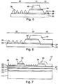
- the figures of FIGS. 3A, 3B and 3C show different embodiments of the texturing in a lateral view, wherein for the sake of simplicity all layers arranged below the upper jacket layer 20 are not shown.
- the texturing has depressions 36, the depressions extending through the current distribution layer 28 and the n + -layer 24 of the tunnel diode 26.
- a cross-section of the recesses 36 is frusto-conical or alternatively trough-shaped. According to the in the FIG. 3C illustrated embodiment, the cross section of the recesses 36 undercuts 38.
- a further embodiment of the recesses 36 of the textured third region 33 is outlined, wherein the recesses 36 each extend through the power distribution layer 28 and through the entire tunnel diode 26 to the lower cladding layer 20.
- FIG. 5 In the picture of the FIG. 5 is a section along the lines AA the FIG. 1 shown. The following are just the differences from the presentation in the FIG. 1 explained. To simplify the presentation, all Layers below the upper cladding layer 20 arranged layers not shown.
- the first region 31 is formed by the n-doped contact layer 34 on the current distribution layer 28.
- a conductor track 40 is arranged on the first region 31.
- the trace 40 is part of a front-side contact of the light-emitting diode 10.
- the third textured region 33 is formed by depressions that run through the current distribution layer and the entire tunnel diode 26.
- FIG. 6 In the picture of the FIG. 6 is a section along the lines BB the FIG. 1 shown. The following are just the differences from the presentation in the FIG. 1 explained. For ease of illustration, all layers below the upper cladding layer 20 are not shown.
- the first region 31 adjoins the textured third region 33 with depressions reaching up to the upper cladding layer 20.
- the first region 31 is formed by the n-doped contact layer 34, which is arranged on the current distribution layer 28.
- the first region 31 is adjoined by the second region 32 formed by the upper cladding layer 20, as a result of which the upper side 30 of the stacked structure has a step in the region of the transition.
- the step is part of a contact hole with a flat floor area.
- an injection barrier 27 is formed in order to suppress a current input against the stacking direction.
- the injection barrier comprises a p / n junction.
- an electrically conductive material Arranged on the first and second regions 31 and 32 is an electrically conductive material which also extends over the step and forms a further part of the front-side contact of the light-emitting diode 10.
- the contact resistance between the electrically conductive material and the second region 32 is at least 10 times greater than the contact resistance between the electrically conductive material and the contact layer 34. This suppresses an undesired current flow directed downwards in the direction of the active layer 18.
- the stack-shaped structure 12 has according to the in FIG. 2B illustrated embodiment, a mirror layer 19, the recesses 36 of the textured third region extend through the entire tunnel diode 26 to the upper cladding layer 20th
Landscapes
- Led Devices (AREA)
Applications Claiming Priority (1)
| Application Number | Priority Date | Filing Date | Title |
|---|---|---|---|
| DE102017002333.6A DE102017002333A1 (de) | 2017-03-13 | 2017-03-13 | Leuchtdiode |
Publications (2)
| Publication Number | Publication Date |
|---|---|
| EP3376547A1 true EP3376547A1 (fr) | 2018-09-19 |
| EP3376547B1 EP3376547B1 (fr) | 2019-03-27 |
Family
ID=61626876
Family Applications (1)
| Application Number | Title | Priority Date | Filing Date |
|---|---|---|---|
| EP18000236.2A Active EP3376547B1 (fr) | 2017-03-13 | 2018-03-09 | Diode électroluminescente |
Country Status (5)
| Country | Link |
|---|---|
| US (2) | US10475963B2 (fr) |
| EP (1) | EP3376547B1 (fr) |
| CN (1) | CN108574028B (fr) |
| DE (1) | DE102017002333A1 (fr) |
| TW (1) | TWI661577B (fr) |
Families Citing this family (2)
| Publication number | Priority date | Publication date | Assignee | Title |
|---|---|---|---|---|
| CN114006267B (zh) * | 2021-11-05 | 2023-10-13 | 中国科学院半导体研究所 | 波长6微米的激光器的有源区和激光器 |
| DE102022120161A1 (de) * | 2022-08-10 | 2024-02-15 | Ams-Osram International Gmbh | Optoelektronisches halbleiterbauelement mit epitaktisch gewachsener schicht und verfahren zur herstellung des optoelektronischen halbleiterbauelements |
Citations (6)
| Publication number | Priority date | Publication date | Assignee | Title |
|---|---|---|---|---|
| US20060267026A1 (en) * | 2005-05-31 | 2006-11-30 | Samsung Electro-Mechanics Co., Ltd. | White light emitting device |
| DE102007032555A1 (de) * | 2007-07-12 | 2009-01-15 | Osram Opto Semiconductors Gmbh | Halbleiterchip und Verfahren zur Herstellung eines Halbleiterchips |
| DE102007035687A1 (de) * | 2007-07-30 | 2009-02-05 | Osram Opto Semiconductors Gmbh | Optoelektronisches Bauelement mit einem Schichtenstapel |
| US20100283081A1 (en) * | 2009-05-08 | 2010-11-11 | Epistar Corporation | Light-emitting device |
| DE102015102857A1 (de) * | 2015-02-27 | 2016-09-01 | Osram Opto Semiconductors Gmbh | Optoelektronisches Halbleiterbauelement, Verfahren zur Herstellung eines elektrischen Kontakts und Verfahren zur Herstellung eines Halbleiterbauelements |
| US20170040492A1 (en) * | 2015-01-16 | 2017-02-09 | Epistar Corporation | Semiconductor light-emitting device |
Family Cites Families (8)
| Publication number | Priority date | Publication date | Assignee | Title |
|---|---|---|---|---|
| US5779924A (en) | 1996-03-22 | 1998-07-14 | Hewlett-Packard Company | Ordered interface texturing for a light emitting device |
| CN1079586C (zh) * | 1999-01-28 | 2002-02-20 | 北京工业大学 | 高效逐级增强高亮度发光二极管及其设计方法 |
| EP2843716A3 (fr) * | 2006-11-15 | 2015-04-29 | The Regents of The University of California | Diode électroluminescente à couche de conversion de phosphore texturée |
| US8058082B2 (en) * | 2008-08-11 | 2011-11-15 | Taiwan Semiconductor Manufacturing Company, Ltd. | Light-emitting diode with textured substrate |
| US8299479B2 (en) * | 2010-03-09 | 2012-10-30 | Tsmc Solid State Lighting Ltd. | Light-emitting devices with textured active layer |
| TWI429110B (zh) * | 2011-01-07 | 2014-03-01 | Nat Univ Tsing Hua | 具有自我複製式光子晶體之發光元件與其製造方法 |
| US8648328B2 (en) * | 2011-12-27 | 2014-02-11 | Sharp Laboratories Of America, Inc. | Light emitting diode (LED) using three-dimensional gallium nitride (GaN) pillar structures with planar surfaces |
| KR101967836B1 (ko) * | 2012-12-14 | 2019-04-10 | 삼성전자주식회사 | 3차원 발광 소자 및 그 제조방법 |
-
2017
- 2017-03-13 DE DE102017002333.6A patent/DE102017002333A1/de not_active Withdrawn
-
2018
- 2018-03-06 TW TW107107346A patent/TWI661577B/zh active
- 2018-03-09 EP EP18000236.2A patent/EP3376547B1/fr active Active
- 2018-03-13 CN CN201810203555.4A patent/CN108574028B/zh active Active
- 2018-03-13 US US15/919,741 patent/US10475963B2/en active Active
-
2019
- 2019-09-18 US US16/574,920 patent/US10615309B2/en active Active
Patent Citations (6)
| Publication number | Priority date | Publication date | Assignee | Title |
|---|---|---|---|---|
| US20060267026A1 (en) * | 2005-05-31 | 2006-11-30 | Samsung Electro-Mechanics Co., Ltd. | White light emitting device |
| DE102007032555A1 (de) * | 2007-07-12 | 2009-01-15 | Osram Opto Semiconductors Gmbh | Halbleiterchip und Verfahren zur Herstellung eines Halbleiterchips |
| DE102007035687A1 (de) * | 2007-07-30 | 2009-02-05 | Osram Opto Semiconductors Gmbh | Optoelektronisches Bauelement mit einem Schichtenstapel |
| US20100283081A1 (en) * | 2009-05-08 | 2010-11-11 | Epistar Corporation | Light-emitting device |
| US20170040492A1 (en) * | 2015-01-16 | 2017-02-09 | Epistar Corporation | Semiconductor light-emitting device |
| DE102015102857A1 (de) * | 2015-02-27 | 2016-09-01 | Osram Opto Semiconductors Gmbh | Optoelektronisches Halbleiterbauelement, Verfahren zur Herstellung eines elektrischen Kontakts und Verfahren zur Herstellung eines Halbleiterbauelements |
Non-Patent Citations (1)
| Title |
|---|
| JEON SEONG-RAN ET AL: "Lateral current spreading in GaN-based light-emitting diodes utilizing tunnel contact junctions", APPLIED PHYSICS LETTERS, A I P PUBLISHING LLC, US, vol. 78, no. 21, 21 May 2001 (2001-05-21), pages 3265 - 3267, XP012028099, ISSN: 0003-6951, DOI: 10.1063/1.1374483 * |
Also Published As
| Publication number | Publication date |
|---|---|
| US10615309B2 (en) | 2020-04-07 |
| US20180261726A1 (en) | 2018-09-13 |
| US20200013927A1 (en) | 2020-01-09 |
| US10475963B2 (en) | 2019-11-12 |
| CN108574028B (zh) | 2020-09-01 |
| DE102017002333A1 (de) | 2018-09-13 |
| CN108574028A (zh) | 2018-09-25 |
| EP3376547B1 (fr) | 2019-03-27 |
| TW201841386A (zh) | 2018-11-16 |
| TWI661577B (zh) | 2019-06-01 |
Similar Documents
| Publication | Publication Date | Title |
|---|---|---|
| DE102012101718B4 (de) | Optoelektronischer Halbleiterchip | |
| DE102011116232B4 (de) | Optoelektronischer Halbleiterchip und Verfahren zu dessen Herstellung | |
| DE69312360T2 (de) | Infrarotes Licht emittierende Halbleitervorrichtung mit in bezug auf die Spaltungsflächen schrägen Seitenflächen und Verfahren zu ihrer Herstellung | |
| DE112017006428T5 (de) | Lichtemittierende Halbleitervorrichtung und Verfahren zu ihrer Herstellung | |
| WO2020229043A2 (fr) | Composant optoélectronique, pixel, agencement d'affichage et procédé | |
| WO2016151112A1 (fr) | Corps semi-conducteur optoélectronique et procédé de fabrication d'un corps semi-conducteur optoélectronique | |
| DE112017000332B4 (de) | Optoelektronisches Bauelement und Verfahren zur Herstellung eines optoelektronischen Bauelements | |
| DE102013104954A1 (de) | Optoelektronisches Bauelement und Verfahren zu seiner Herstellung | |
| WO2023105036A1 (fr) | Composant optoélectronique, dispositif optoélectronique et procédé de fabrication d'un composant | |
| EP3376547B1 (fr) | Diode électroluminescente | |
| DE112015002498B4 (de) | Optoelektronischer Halbleiterchip und Verfahren zu dessen Herstellung | |
| DE102017002332B4 (de) | Leuchtdiode | |
| EP3249700B1 (fr) | Diode électroluminescente | |
| DE102024103984A1 (de) | Laservorrichtung und verfahren | |
| DE102006059612A1 (de) | Halbleiterbauelement und Verfahren zu dessen Herstellung | |
| DE19963550B4 (de) | Bipolare Beleuchtungsquelle aus einem einseitig kontaktierten, selbstbündelnden Halbleiterkörper | |
| DE102022119108A1 (de) | Optoelektronisches halbleiterbauelement und verfahren zur herstellung zumindest eines optoelektronischen halbleiterbauelements | |
| WO2014095353A1 (fr) | Procédé de fabrication d'une puce de semi-conducteur optoélectronique et puce de semi-conducteur optoélectronique | |
| WO2023041704A1 (fr) | Puce à semi-conducteur émettrice de lumière et procédé de fabrication d'une puce à semi-conducteur émettrice de lumière | |
| WO2021175635A1 (fr) | Corps semi-conducteur émetteur de rayonnement et son procédé de production | |
| DE112021007846T5 (de) | Optoelektronisches bauelement und verfahren zu dessen herstellung | |
| DE102020126442A1 (de) | Optoelektronische vorrichtung mit einer kontaktschicht und einer darüber angeordneten aufrauschicht sowie herstellungsverfahren | |
| WO2019224154A1 (fr) | Puce de semi-conducteur optoélectronique et procédé de fabrication d'une puce de semi-conducteur optoélectronique | |
| DE102020001353B3 (de) | Stapelförmiges photonisches lll-V-Halbleiterbauelement und Optokoppler | |
| WO2020234163A1 (fr) | Puce en semiconducteur optoélectronique et procédé de fabrication d'une puce en semiconducteur optoélectronique |
Legal Events
| Date | Code | Title | Description |
|---|---|---|---|
| PUAI | Public reference made under article 153(3) epc to a published international application that has entered the european phase |
Free format text: ORIGINAL CODE: 0009012 |
|
| STAA | Information on the status of an ep patent application or granted ep patent |
Free format text: STATUS: REQUEST FOR EXAMINATION WAS MADE |
|
| 17P | Request for examination filed |
Effective date: 20180731 |
|
| AK | Designated contracting states |
Kind code of ref document: A1 Designated state(s): AL AT BE BG CH CY CZ DE DK EE ES FI FR GB GR HR HU IE IS IT LI LT LU LV MC MK MT NL NO PL PT RO RS SE SI SK SM TR |
|
| AX | Request for extension of the european patent |
Extension state: BA ME |
|
| GRAP | Despatch of communication of intention to grant a patent |
Free format text: ORIGINAL CODE: EPIDOSNIGR1 |
|
| STAA | Information on the status of an ep patent application or granted ep patent |
Free format text: STATUS: GRANT OF PATENT IS INTENDED |
|
| INTG | Intention to grant announced |
Effective date: 20181210 |
|
| GRAS | Grant fee paid |
Free format text: ORIGINAL CODE: EPIDOSNIGR3 |
|
| GRAA | (expected) grant |
Free format text: ORIGINAL CODE: 0009210 |
|
| STAA | Information on the status of an ep patent application or granted ep patent |
Free format text: STATUS: THE PATENT HAS BEEN GRANTED |
|
| AK | Designated contracting states |
Kind code of ref document: B1 Designated state(s): AL AT BE BG CH CY CZ DE DK EE ES FI FR GB GR HR HU IE IS IT LI LT LU LV MC MK MT NL NO PL PT RO RS SE SI SK SM TR |
|
| REG | Reference to a national code |
Ref country code: GB Ref legal event code: FG4D Free format text: NOT ENGLISH |
|
| REG | Reference to a national code |
Ref country code: CH Ref legal event code: EP |
|
| REG | Reference to a national code |
Ref country code: AT Ref legal event code: REF Ref document number: 1114074 Country of ref document: AT Kind code of ref document: T Effective date: 20190415 |
|
| REG | Reference to a national code |
Ref country code: IE Ref legal event code: FG4D Free format text: LANGUAGE OF EP DOCUMENT: GERMAN |
|
| REG | Reference to a national code |
Ref country code: DE Ref legal event code: R096 Ref document number: 502018000010 Country of ref document: DE |
|
| PG25 | Lapsed in a contracting state [announced via postgrant information from national office to epo] |
Ref country code: LT Free format text: LAPSE BECAUSE OF FAILURE TO SUBMIT A TRANSLATION OF THE DESCRIPTION OR TO PAY THE FEE WITHIN THE PRESCRIBED TIME-LIMIT Effective date: 20190327 Ref country code: SE Free format text: LAPSE BECAUSE OF FAILURE TO SUBMIT A TRANSLATION OF THE DESCRIPTION OR TO PAY THE FEE WITHIN THE PRESCRIBED TIME-LIMIT Effective date: 20190327 Ref country code: FI Free format text: LAPSE BECAUSE OF FAILURE TO SUBMIT A TRANSLATION OF THE DESCRIPTION OR TO PAY THE FEE WITHIN THE PRESCRIBED TIME-LIMIT Effective date: 20190327 Ref country code: NO Free format text: LAPSE BECAUSE OF FAILURE TO SUBMIT A TRANSLATION OF THE DESCRIPTION OR TO PAY THE FEE WITHIN THE PRESCRIBED TIME-LIMIT Effective date: 20190627 |
|
| REG | Reference to a national code |
Ref country code: NL Ref legal event code: MP Effective date: 20190327 |
|
| PG25 | Lapsed in a contracting state [announced via postgrant information from national office to epo] |
Ref country code: BG Free format text: LAPSE BECAUSE OF FAILURE TO SUBMIT A TRANSLATION OF THE DESCRIPTION OR TO PAY THE FEE WITHIN THE PRESCRIBED TIME-LIMIT Effective date: 20190627 Ref country code: LV Free format text: LAPSE BECAUSE OF FAILURE TO SUBMIT A TRANSLATION OF THE DESCRIPTION OR TO PAY THE FEE WITHIN THE PRESCRIBED TIME-LIMIT Effective date: 20190327 Ref country code: RS Free format text: LAPSE BECAUSE OF FAILURE TO SUBMIT A TRANSLATION OF THE DESCRIPTION OR TO PAY THE FEE WITHIN THE PRESCRIBED TIME-LIMIT Effective date: 20190327 Ref country code: GR Free format text: LAPSE BECAUSE OF FAILURE TO SUBMIT A TRANSLATION OF THE DESCRIPTION OR TO PAY THE FEE WITHIN THE PRESCRIBED TIME-LIMIT Effective date: 20190628 Ref country code: HR Free format text: LAPSE BECAUSE OF FAILURE TO SUBMIT A TRANSLATION OF THE DESCRIPTION OR TO PAY THE FEE WITHIN THE PRESCRIBED TIME-LIMIT Effective date: 20190327 Ref country code: NL Free format text: LAPSE BECAUSE OF FAILURE TO SUBMIT A TRANSLATION OF THE DESCRIPTION OR TO PAY THE FEE WITHIN THE PRESCRIBED TIME-LIMIT Effective date: 20190327 |
|
| PG25 | Lapsed in a contracting state [announced via postgrant information from national office to epo] |
Ref country code: ES Free format text: LAPSE BECAUSE OF FAILURE TO SUBMIT A TRANSLATION OF THE DESCRIPTION OR TO PAY THE FEE WITHIN THE PRESCRIBED TIME-LIMIT Effective date: 20190327 Ref country code: CZ Free format text: LAPSE BECAUSE OF FAILURE TO SUBMIT A TRANSLATION OF THE DESCRIPTION OR TO PAY THE FEE WITHIN THE PRESCRIBED TIME-LIMIT Effective date: 20190327 Ref country code: RO Free format text: LAPSE BECAUSE OF FAILURE TO SUBMIT A TRANSLATION OF THE DESCRIPTION OR TO PAY THE FEE WITHIN THE PRESCRIBED TIME-LIMIT Effective date: 20190327 Ref country code: EE Free format text: LAPSE BECAUSE OF FAILURE TO SUBMIT A TRANSLATION OF THE DESCRIPTION OR TO PAY THE FEE WITHIN THE PRESCRIBED TIME-LIMIT Effective date: 20190327 Ref country code: IT Free format text: LAPSE BECAUSE OF FAILURE TO SUBMIT A TRANSLATION OF THE DESCRIPTION OR TO PAY THE FEE WITHIN THE PRESCRIBED TIME-LIMIT Effective date: 20190327 Ref country code: SK Free format text: LAPSE BECAUSE OF FAILURE TO SUBMIT A TRANSLATION OF THE DESCRIPTION OR TO PAY THE FEE WITHIN THE PRESCRIBED TIME-LIMIT Effective date: 20190327 Ref country code: PT Free format text: LAPSE BECAUSE OF FAILURE TO SUBMIT A TRANSLATION OF THE DESCRIPTION OR TO PAY THE FEE WITHIN THE PRESCRIBED TIME-LIMIT Effective date: 20190727 Ref country code: AL Free format text: LAPSE BECAUSE OF FAILURE TO SUBMIT A TRANSLATION OF THE DESCRIPTION OR TO PAY THE FEE WITHIN THE PRESCRIBED TIME-LIMIT Effective date: 20190327 |
|
| PG25 | Lapsed in a contracting state [announced via postgrant information from national office to epo] |
Ref country code: PL Free format text: LAPSE BECAUSE OF FAILURE TO SUBMIT A TRANSLATION OF THE DESCRIPTION OR TO PAY THE FEE WITHIN THE PRESCRIBED TIME-LIMIT Effective date: 20190327 Ref country code: SM Free format text: LAPSE BECAUSE OF FAILURE TO SUBMIT A TRANSLATION OF THE DESCRIPTION OR TO PAY THE FEE WITHIN THE PRESCRIBED TIME-LIMIT Effective date: 20190327 |
|
| PG25 | Lapsed in a contracting state [announced via postgrant information from national office to epo] |
Ref country code: IS Free format text: LAPSE BECAUSE OF FAILURE TO SUBMIT A TRANSLATION OF THE DESCRIPTION OR TO PAY THE FEE WITHIN THE PRESCRIBED TIME-LIMIT Effective date: 20190727 |
|
| REG | Reference to a national code |
Ref country code: DE Ref legal event code: R097 Ref document number: 502018000010 Country of ref document: DE |
|
| PG25 | Lapsed in a contracting state [announced via postgrant information from national office to epo] |
Ref country code: DK Free format text: LAPSE BECAUSE OF FAILURE TO SUBMIT A TRANSLATION OF THE DESCRIPTION OR TO PAY THE FEE WITHIN THE PRESCRIBED TIME-LIMIT Effective date: 20190327 |
|
| PLBE | No opposition filed within time limit |
Free format text: ORIGINAL CODE: 0009261 |
|
| STAA | Information on the status of an ep patent application or granted ep patent |
Free format text: STATUS: NO OPPOSITION FILED WITHIN TIME LIMIT |
|
| 26N | No opposition filed |
Effective date: 20200103 |
|
| PG25 | Lapsed in a contracting state [announced via postgrant information from national office to epo] |
Ref country code: TR Free format text: LAPSE BECAUSE OF FAILURE TO SUBMIT A TRANSLATION OF THE DESCRIPTION OR TO PAY THE FEE WITHIN THE PRESCRIBED TIME-LIMIT Effective date: 20190327 |
|
| PG25 | Lapsed in a contracting state [announced via postgrant information from national office to epo] |
Ref country code: MC Free format text: LAPSE BECAUSE OF FAILURE TO SUBMIT A TRANSLATION OF THE DESCRIPTION OR TO PAY THE FEE WITHIN THE PRESCRIBED TIME-LIMIT Effective date: 20190327 |
|
| REG | Reference to a national code |
Ref country code: BE Ref legal event code: MM Effective date: 20200331 |
|
| PG25 | Lapsed in a contracting state [announced via postgrant information from national office to epo] |
Ref country code: LU Free format text: LAPSE BECAUSE OF NON-PAYMENT OF DUE FEES Effective date: 20200309 |
|
| PG25 | Lapsed in a contracting state [announced via postgrant information from national office to epo] |
Ref country code: IE Free format text: LAPSE BECAUSE OF NON-PAYMENT OF DUE FEES Effective date: 20200309 |
|
| PG25 | Lapsed in a contracting state [announced via postgrant information from national office to epo] |
Ref country code: BE Free format text: LAPSE BECAUSE OF NON-PAYMENT OF DUE FEES Effective date: 20200331 |
|
| REG | Reference to a national code |
Ref country code: CH Ref legal event code: PL |
|
| PG25 | Lapsed in a contracting state [announced via postgrant information from national office to epo] |
Ref country code: CH Free format text: LAPSE BECAUSE OF NON-PAYMENT OF DUE FEES Effective date: 20210331 Ref country code: LI Free format text: LAPSE BECAUSE OF NON-PAYMENT OF DUE FEES Effective date: 20210331 |
|
| PG25 | Lapsed in a contracting state [announced via postgrant information from national office to epo] |
Ref country code: MT Free format text: LAPSE BECAUSE OF FAILURE TO SUBMIT A TRANSLATION OF THE DESCRIPTION OR TO PAY THE FEE WITHIN THE PRESCRIBED TIME-LIMIT Effective date: 20190327 Ref country code: CY Free format text: LAPSE BECAUSE OF FAILURE TO SUBMIT A TRANSLATION OF THE DESCRIPTION OR TO PAY THE FEE WITHIN THE PRESCRIBED TIME-LIMIT Effective date: 20190327 |
|
| PG25 | Lapsed in a contracting state [announced via postgrant information from national office to epo] |
Ref country code: MK Free format text: LAPSE BECAUSE OF FAILURE TO SUBMIT A TRANSLATION OF THE DESCRIPTION OR TO PAY THE FEE WITHIN THE PRESCRIBED TIME-LIMIT Effective date: 20190327 |
|
| PG25 | Lapsed in a contracting state [announced via postgrant information from national office to epo] |
Ref country code: SI Free format text: LAPSE BECAUSE OF FAILURE TO SUBMIT A TRANSLATION OF THE DESCRIPTION OR TO PAY THE FEE WITHIN THE PRESCRIBED TIME-LIMIT Effective date: 20190327 |
|
| REG | Reference to a national code |
Ref country code: AT Ref legal event code: MM01 Ref document number: 1114074 Country of ref document: AT Kind code of ref document: T Effective date: 20230309 |
|
| PG25 | Lapsed in a contracting state [announced via postgrant information from national office to epo] |
Ref country code: AT Free format text: LAPSE BECAUSE OF NON-PAYMENT OF DUE FEES Effective date: 20230309 |
|
| PG25 | Lapsed in a contracting state [announced via postgrant information from national office to epo] |
Ref country code: AT Free format text: LAPSE BECAUSE OF NON-PAYMENT OF DUE FEES Effective date: 20230309 |
|
| P01 | Opt-out of the competence of the unified patent court (upc) registered |
Free format text: CASE NUMBER: APP_40043/2024 Effective date: 20240704 |
|
| REG | Reference to a national code |
Ref country code: DE Ref legal event code: R079 Ref document number: 502018000010 Country of ref document: DE Free format text: PREVIOUS MAIN CLASS: H01L0033140000 Ipc: H10H0020816000 |
|
| PGFP | Annual fee paid to national office [announced via postgrant information from national office to epo] |
Ref country code: GB Payment date: 20260324 Year of fee payment: 9 |
|
| PGFP | Annual fee paid to national office [announced via postgrant information from national office to epo] |
Ref country code: DE Payment date: 20260319 Year of fee payment: 9 |
|
| PGFP | Annual fee paid to national office [announced via postgrant information from national office to epo] |
Ref country code: AT Payment date: 20260410 Year of fee payment: 5 |
|
| PGFP | Annual fee paid to national office [announced via postgrant information from national office to epo] |
Ref country code: FR Payment date: 20260320 Year of fee payment: 9 |