EP3379271A1 - Kapazitätsdetektor, elektronische vorrichtung und druckdetektor - Google Patents
Kapazitätsdetektor, elektronische vorrichtung und druckdetektor Download PDFInfo
- Publication number
- EP3379271A1 EP3379271A1 EP17849895.2A EP17849895A EP3379271A1 EP 3379271 A1 EP3379271 A1 EP 3379271A1 EP 17849895 A EP17849895 A EP 17849895A EP 3379271 A1 EP3379271 A1 EP 3379271A1
- Authority
- EP
- European Patent Office
- Prior art keywords
- switch
- capacitor
- detected
- operational amplifier
- capacitance
- Prior art date
- Legal status (The legal status is an assumption and is not a legal conclusion. Google has not performed a legal analysis and makes no representation as to the accuracy of the status listed.)
- Granted
Links
Images


Classifications
-
- G—PHYSICS
- G06—COMPUTING OR CALCULATING; COUNTING
- G06F—ELECTRIC DIGITAL DATA PROCESSING
- G06F3/00—Input arrangements for transferring data to be processed into a form capable of being handled by the computer; Output arrangements for transferring data from processing unit to output unit, e.g. interface arrangements
- G06F3/01—Input arrangements or combined input and output arrangements for interaction between user and computer
- G06F3/03—Arrangements for converting the position or the displacement of a member into a coded form
- G06F3/041—Digitisers, e.g. for touch screens or touch pads, characterised by the transducing means
- G06F3/0414—Digitisers, e.g. for touch screens or touch pads, characterised by the transducing means using force sensing means to determine a position
-
- G—PHYSICS
- G01—MEASURING; TESTING
- G01L—MEASURING FORCE, STRESS, TORQUE, WORK, MECHANICAL POWER, MECHANICAL EFFICIENCY, OR FLUID PRESSURE
- G01L1/00—Measuring force or stress, in general
- G01L1/14—Measuring force or stress, in general by measuring variations in capacitance or inductance of electrical elements, e.g. by measuring variations of frequency of electrical oscillators
- G01L1/142—Measuring force or stress, in general by measuring variations in capacitance or inductance of electrical elements, e.g. by measuring variations of frequency of electrical oscillators using capacitors
- G01L1/144—Measuring force or stress, in general by measuring variations in capacitance or inductance of electrical elements, e.g. by measuring variations of frequency of electrical oscillators using capacitors with associated circuitry
-
- G—PHYSICS
- G06—COMPUTING OR CALCULATING; COUNTING
- G06F—ELECTRIC DIGITAL DATA PROCESSING
- G06F3/00—Input arrangements for transferring data to be processed into a form capable of being handled by the computer; Output arrangements for transferring data from processing unit to output unit, e.g. interface arrangements
- G06F3/01—Input arrangements or combined input and output arrangements for interaction between user and computer
- G06F3/03—Arrangements for converting the position or the displacement of a member into a coded form
- G06F3/041—Digitisers, e.g. for touch screens or touch pads, characterised by the transducing means
- G06F3/0416—Control or interface arrangements specially adapted for digitisers
-
- G—PHYSICS
- G06—COMPUTING OR CALCULATING; COUNTING
- G06F—ELECTRIC DIGITAL DATA PROCESSING
- G06F3/00—Input arrangements for transferring data to be processed into a form capable of being handled by the computer; Output arrangements for transferring data from processing unit to output unit, e.g. interface arrangements
- G06F3/01—Input arrangements or combined input and output arrangements for interaction between user and computer
- G06F3/03—Arrangements for converting the position or the displacement of a member into a coded form
- G06F3/041—Digitisers, e.g. for touch screens or touch pads, characterised by the transducing means
- G06F3/0416—Control or interface arrangements specially adapted for digitisers
- G06F3/0418—Control or interface arrangements specially adapted for digitisers for error correction or compensation, e.g. based on parallax, calibration or alignment
-
- G—PHYSICS
- G06—COMPUTING OR CALCULATING; COUNTING
- G06F—ELECTRIC DIGITAL DATA PROCESSING
- G06F3/00—Input arrangements for transferring data to be processed into a form capable of being handled by the computer; Output arrangements for transferring data from processing unit to output unit, e.g. interface arrangements
- G06F3/01—Input arrangements or combined input and output arrangements for interaction between user and computer
- G06F3/03—Arrangements for converting the position or the displacement of a member into a coded form
- G06F3/041—Digitisers, e.g. for touch screens or touch pads, characterised by the transducing means
- G06F3/044—Digitisers, e.g. for touch screens or touch pads, characterised by the transducing means by capacitive means
-
- G—PHYSICS
- G06—COMPUTING OR CALCULATING; COUNTING
- G06F—ELECTRIC DIGITAL DATA PROCESSING
- G06F3/00—Input arrangements for transferring data to be processed into a form capable of being handled by the computer; Output arrangements for transferring data from processing unit to output unit, e.g. interface arrangements
- G06F3/01—Input arrangements or combined input and output arrangements for interaction between user and computer
- G06F3/03—Arrangements for converting the position or the displacement of a member into a coded form
- G06F3/041—Digitisers, e.g. for touch screens or touch pads, characterised by the transducing means
- G06F3/044—Digitisers, e.g. for touch screens or touch pads, characterised by the transducing means by capacitive means
- G06F3/0447—Position sensing using the local deformation of sensor cells
-
- H—ELECTRICITY
- H03—ELECTRONIC CIRCUITRY
- H03F—AMPLIFIERS
- H03F3/00—Amplifiers with only discharge tubes or only semiconductor devices as amplifying elements
- H03F3/45—Differential amplifiers
- H03F3/45071—Differential amplifiers with semiconductor devices only
- H03F3/45076—Differential amplifiers with semiconductor devices only characterised by the way of implementation of the active amplifying circuit in the differential amplifier
- H03F3/45475—Differential amplifiers with semiconductor devices only characterised by the way of implementation of the active amplifying circuit in the differential amplifier using IC blocks as the active amplifying circuit
-
- H—ELECTRICITY
- H03—ELECTRONIC CIRCUITRY
- H03F—AMPLIFIERS
- H03F2200/00—Indexing scheme relating to amplifiers
- H03F2200/261—Amplifier which being suitable for instrumentation applications
-
- H—ELECTRICITY
- H03—ELECTRONIC CIRCUITRY
- H03F—AMPLIFIERS
- H03F2203/00—Indexing scheme relating to amplifiers with only discharge tubes or only semiconductor devices as amplifying elements covered by H03F3/00
- H03F2203/45—Indexing scheme relating to differential amplifiers
- H03F2203/45116—Feedback coupled to the input of the differential amplifier
-
- H—ELECTRICITY
- H03—ELECTRONIC CIRCUITRY
- H03F—AMPLIFIERS
- H03F2203/00—Indexing scheme relating to amplifiers with only discharge tubes or only semiconductor devices as amplifying elements covered by H03F3/00
- H03F2203/45—Indexing scheme relating to differential amplifiers
- H03F2203/45138—Two or more differential amplifiers in IC-block form are combined, e.g. measuring amplifiers
-
- H—ELECTRICITY
- H03—ELECTRONIC CIRCUITRY
- H03F—AMPLIFIERS
- H03F2203/00—Indexing scheme relating to amplifiers with only discharge tubes or only semiconductor devices as amplifying elements covered by H03F3/00
- H03F2203/45—Indexing scheme relating to differential amplifiers
- H03F2203/45156—At least one capacitor being added at the input of a dif amp
-
- H—ELECTRICITY
- H03—ELECTRONIC CIRCUITRY
- H03F—AMPLIFIERS
- H03F2203/00—Indexing scheme relating to amplifiers with only discharge tubes or only semiconductor devices as amplifying elements covered by H03F3/00
- H03F2203/45—Indexing scheme relating to differential amplifiers
- H03F2203/45514—Indexing scheme relating to differential amplifiers the FBC comprising one or more switched capacitors, and being coupled between the LC and the IC
Definitions
- the present disclosure relates to the field of information technologies, and more specifically, to an apparatus for detecting capacitance, an electronic device and an apparatus for detecting a force.
- a capacitive sensor such as a capacitive touch screen, a capacitive force sensor and a capacitive displacement sensor, to detect an external physical signal.
- a capacitance detection technology is a key technology of realizing the capacitive sensor, and a capacitance change of a capacitor is detected through the capacitance detection technology so as to detect a signal to be detected.
- An accuracy of detecting capacitance decides an accuracy of signal detection. Therefore, how to improve the accuracy of detecting the capacitance is a technical problem to be solved urgently.
- Embodiments of the present disclosure provide an apparatus for detecting capacitance, an electronic device and an apparatus for detecting a force, which could improve an accuracy of capacitance detection.
- an apparatus for detecting capacitance including:
- the apparatus for detecting capacitance of the embodiments of the present disclosure may detect a slight capacitance change, and may improve the accuracy of capacitance detection.
- the at least one capacitor to be detected includes a first capacitor 101 to be detected; and a differential mode signal of voltage signals at different times which are output by the conversion circuit 120 represents a capacitance change of the first capacitor 101 to be detected.
- the signal driving circuit 110 includes a first switch 111, a second switch 112, a third switch 113 and a first direct current voltage source 115; and one end of the first capacitor 101 to be detected is connected to the first direct current voltage source 115 via the third switch 113 and the first switch 111, the one end of the first capacitor 101 to be detected is grounded via the third switch 113 and the second switch 112, and the other end of the first capacitor 101 to be detected is grounded.
- the conversion circuit 120 includes a fourth switch 121, a fifth switch 122, a first feedback capacitor 123 and a first operational amplifier 124; the fourth switch 121 is connected between one end of the first capacitor 101 to be detected and an inverting input of the first operational amplifier 124; the first feedback capacitor 123 is connected between the inverting input and an output of the first operational amplifier 124; the fifth switch 122 is connected between the inverting input and the output of the first operational amplifier 124; and a common mode voltage Vcm is input to a non-inverting input of the first operational amplifier 124.
- the cancellation circuit 130 includes a first adjustable capacitor 131, a sixth switch 132, a seventh switch 133, an eighth switch 134, a ninth switch 135 and a second direct current voltage source 139; one end of the first adjustable capacitor 131 is connected to the second direct current voltage source 139 via the sixth switch 132, the one end of the first adjustable capacitor 131 is grounded via the seventh switch 133, and the other end of the first adjustable capacitor 131 is connected to the inverting input of the first operational amplifier 124; and the eighth switch 134 and the ninth switch 135 are configured to change switch control signals controlling the sixth switch 132 and the seventh switch 133.
- the apparatus for detecting capacitance of the embodiments of the present disclosure has an excellent ability of suppressing low-band common-mode noise and 1/f noise.
- the at least one capacitor to be detected includes a first capacitor 101 to be detected and a second capacitor 102 to be detected; and a differential signal of voltage signals which are output by the conversion circuit 120 and are corresponding to the first capacitor 101 to be detected and the second capacitor 102 to be detected represents a capacitance change of the first capacitor 101 to be detected and the second capacitor 102 to be detected.
- the signal driving circuit 110 includes a first switch 111, a second switch 112, a third switch 113, a tenth switch 114 and a first direct current voltage source 115; one end of the first capacitor 101 to be detected is connected to the first direct current voltage source 115 via the third switch 113 and the first switch 111, the one end of the first capacitor 101 to be detected is grounded via the third switch 113 and the second switch 112, and the other end of the first capacitor 101 to be detected is grounded; and one end of the second capacitor 102 to be detected is connected to the first direct current voltage source 115 via the tenth switch 114 and the first switch 111, the one end of the second capacitor 102 to be detected is grounded via the tenth switch 114 and the second switch 112, and the other end of the second capacitor 102 to be detected is grounded.
- the conversion circuit 120 includes a fourth switch 121, a fifth switch 122, a first feedback capacitor 123, a first operational amplifier 124, an eleventh switch 125, a twelfth switch 126, a second feedback capacitor 127 and a second operational amplifier 128;
- the fourth switch 121 is connected between one end of the first capacitor 101 to be detected and an inverting input of the first operational amplifier 124;
- the first feedback capacitor 123 is connected between the inverting input and an output of the first operational amplifier 124;
- the fifth switch 122 is connected between the inverting input and the output of the first operational amplifier 124;
- the eleventh switch 125 is connected between one end of the second capacitor 102 to be detected and an inverting input of the second operational amplifier 128;
- the second feedback capacitor 127 is connected between the inverting input and an output of the second operational amplifier 128;
- the twelfth switch 126 is connected between the inverting input and the output of the second operational amplifier 128; and a common mode
- the cancellation circuit 130 includes a first adjustable capacitor 131, a sixth switch 132, a seventh switch 133, an eighth switch 134, a ninth switch 135, a second adjustable capacitor 136, a thirteenth switch 137, a fourteenth switch 138 and a second direct current voltage source 139; one end of the first adjustable capacitor 131 is connected to the second direct current voltage source 139 via the sixth switch 132, the one end of the first adjustable capacitor 131 is grounded via the seventh switch 133, and the other end of the first adjustable capacitor 131 is connected to the inverting input of the first operational amplifier 124; one end of the second adjustable capacitor 136 is connected to the second direct current voltage source 139 via the thirteenth switch 137, the one end of the second adjustable capacitor 136 is grounded via the fourteenth switch 138, and the other end of the second adjustable capacitor 136 is connected to the inverting input of the second operational amplifier 128; and the eighth switch 134 and the ninth switch 135 are configured to change switch control signals controlling the sixth switch 132, the
- the apparatus further includes: a programmable gain amplifier 140, configured to output a differential signal according to voltage signals corresponding to the first capacitor 101 to be detected and the second capacitor 102 to be detected.
- a programmable gain amplifier 140 configured to output a differential signal according to voltage signals corresponding to the first capacitor 101 to be detected and the second capacitor 102 to be detected.
- an output voltage of the first direct current voltage source 115 is equal to that of the second direct current voltage source 139.
- the output voltage is twice the magnitude of the common mode voltage Vcm.
- the first capacitor to be detected and the second capacitor to be detected are capacitors in a differential capacitive sensor.
- the apparatus for detecting capacitance of the embodiments of the present disclosure has an excellent ability of suppressing a temperature drift.
- an electronic device including the apparatus for detecting capacitance in the first aspect or any one of the possible implementation manners of the first aspect.
- an apparatus for detecting a force including the apparatus for detecting capacitance in the first aspect or any one of the possible implementation manners of the first aspect, where a force which is to be detected by the apparatus for detecting a force is associated with a capacitance change of a capacitor to be detected which is to be detected by the apparatus for detecting capacitance.
- inventions of the present disclosure may be applied to various devices adopting a touch technology, for example, an active pen, a capacitive pen, a mobile terminal, a computer, a home appliance, etc.
- An apparatus for detecting capacitance of the embodiments of the present disclosure may be disposed in various touch devices so as to be used to detect a touch capacitor, i.e., a capacitance change of a capacitor to be detected, and then detect a change of a force generated by a touch, etc.
- the capacitance change of the capacitor to be detected may either be a relative value, or be an absolute value, for example, in the case where initial capacitance of the capacitor to be detected is zero, the capacitance change of the capacitor to be detected is an absolute value of capacitance of the capacitor.
- capacitor may also be called “capacitance” for short, and correspondingly capacitance of the capacitor may also be called a capacitance value.
- capacitance for short, and correspondingly capacitance of the capacitor may also be called a capacitance value.
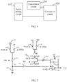
- FIG. 1 shows a schematic diagram of an apparatus for detecting capacitance of an embodiment of the present disclosure.
- the apparatus may include a signal driving circuit 110, a conversion circuit 120 and a cancellation circuit 130.
- the signal driving circuit 110 is configured to periodically charge and discharge at least one capacitor to be detected.
- the signal driving circuit 110 may also be called a driving circuit, and for example, it could realize charging and discharging of a capacitor to be detected via switchover.
- the conversion circuit 120 is configured to convert a capacitance signal of the at least one capacitor to be detected into a voltage signal.
- the conversion circuit 120 is a capacitance/voltage (C/V) converting circuit, for example, it can convert a capacitance signal into a voltage signal via an operational amplifier and a feedback circuit.
- C/V capacitance/voltage
- the cancellation circuit 130 is configured to cancel initial capacitance of the at least one capacitor to be detected, so that the voltage signal is associated with a capacitance change of the at least one capacitor to be detected.
- initial capacitance (including parasitic capacitance) of a capacitor to be detected is canceled via the cancellation circuit 130, for example, the initial capacitance of the capacitor to be detected is canceled via an adjustable capacitor, so that an output is zero when capacitance of the capacitor to be detected is not changed, thus making an output signal of the conversion circuit 120 associated with a capacitance change of the capacitor to be detected.
- An initial value is set as zero by adopting a cancellation circuit, which thus could improve a dynamic range of capacitance detection.
- the at least one capacitor to be detected includes a first capacitor to be detected; and a differential mode signal of voltage signals at different times which are output by the conversion circuit 120 represents a capacitance change of the first capacitor to be detected.
- a differential mode signal of voltage signals at different times which are output via the conversion circuit 120 reflects a capacitance change of this one capacitor to be detected.
- FIG. 2 shows a schematic diagram of a specific implementation manner of an apparatus for detecting capacitance of an embodiment of the present disclosure.
- FIG. 2 is merely an example, and is not intended to limit the scope of the embodiments of the present disclosure.
- the signal driving circuit 110 in FIG. 1 may include a first switch 111, a second switch 112, a third switch 113 and a first direct current voltage source 115.
- One end of the first capacitor 101 to be detected is connected to the first direct current voltage source 115 via the third switch 113 and the first switch 111, the one end is grounded via the third switch 113 and the second switch 112, and the other end of the first capacitor 101 to be detected is grounded.
- the first switch 111 is controlled through a first switch control signal (denoted as PNSW), the second switch 112 is controlled through an inverted signal PNSW of PNSW, and the third switch 113 is controlled through a second switch control signal (denoted as SW).
- PNSW first switch control signal
- SW second switch control signal
- the first capacitor 101 to be detected is charged by the first direct current voltage source 115.
- An output voltage of the first direct current voltage source 115 may be denoted as Vdc.
- the conversion circuit 120 in FIG. 1 may include a fourth switch 121, a fifth switch 122, a first feedback capacitor 123 and a first operational amplifier 124.
- the fourth switch 121 is controlled through an inverted signal SW of SW, and the fifth switch 122 is controlled through SW.
- the fourth switch 121 is connected between one end of the first capacitor 101 to be detected and an inverting input of the first operational amplifier 124; the first feedback capacitor 123 is connected between the inverting input and an output of the first operational amplifier 124; the fifth switch 122 is connected between the inverting input and the output of the first operational amplifier 124; and a common mode voltage Vcm is input to a non-inverting input of the first operational amplifier 124.
- the cancellation circuit 130 in FIG. 1 may include a first adjustable capacitor 131, a sixth switch 132, a seventh switch 133, an eighth switch 134, a ninth switch 135 and a second direct current voltage source 139.
- Output voltages of the second direct current voltage source 139 and the first direct current voltage source 115 are equal, i.e., both of them are Vdc.
- the eighth switch 134 is controlled through PNSW
- the ninth switch 135 is controlled through the inverted signal PNSW of PNSW
- the sixth switch 132 is controlled through a third switch control signal CSW
- the seventh switch 133 is controlled through an inverted signal CSW of CSW.
- One end of the first adjustable capacitor 131 is connected to the second direct current voltage source 139 via the sixth switch 132, the one end is grounded via the seventh switch 133, and the other end of the first adjustable capacitor 131 is connected to the inverting input of the first operational amplifier 124; and the eighth switch 134 and the ninth switch 135 are configured to change switch control signals controlling the sixth switch 132 and the seventh switch 133.
- CSW and CSW are switch control signals of the sixth switch 132 and the seventh switch 133, respectively.
- CSW is equal to SW; and when the eighth switch 34 is switched off and the ninth switch 135 is switched on, CSW is equal to SW .
- the sixth switch 132 and the seventh switch 133 are then controlled by CSW and CSW , respectively.
- the first switch control signal PNSW and the second switch control signal SW in FIG. 2 may use signals as shown in FIG. 3
- FIG. 2 A working principle of a circuit shown in FIG. 2 is described below in combination with FIG. 3 .
- a complete capacitance detection cycle consists of t1, t2, t3 and t4.
- a detecting time sequence is a time sequence of driving a signal positively and negatively.
- a subsequent stage sampling circuit may obtain a magnitude of a differential mode signal by sampling and subtracting outputs of Vout at t2 and t4:
- initial capacitance C1 0 is completely canceled, thus the magnitude of the differential mode signal output is:
- Vou t DM Vdc ⁇ ⁇ C Cfb
- ⁇ C represents a change of capacitance of the first capacitor 101 to be detected.
- the apparatus for detecting capacitance of the embodiments of the present disclosure has an excellent ability of suppressing low-band common noise and 1/f noise (also called flicker noise). That is to say, the apparatus for detecting capacitance of the embodiments of the present disclosure may improve the anti-interference performance, and in this way, capacitance to be detected may also be detected when it is changed slightly. Therefore, the apparatus for detecting capacitance of the embodiments of the present disclosure may detect a slight capacitance change, and may improve the accuracy of capacitance detection.
- the above cancellation circuit of the embodiments of the present disclosure may cancel the initial capacitance completely, and has higher cancellation efficiency.
- the at least one capacitor to be detected includes a first capacitor to be detected and a second capacitor to be detected; and a differential signal of voltage signals which are output by the conversion circuit 120 and are corresponding to the first capacitor to be detected and the second capacitor to be detected represents a capacitance change of the first capacitor to be detected and the second capacitor to be detected.
- a differential signal of voltage signals which are output via the conversion circuit 120 and are corresponding to two capacitors to be detected reflects a capacitance change of the two capacitors to be detected.
- capacitance of one of the capacitors to be detected may be changed and capacitance of the other one of the capacitors to be detected may not be changed, and the capacitance that is not changed may be standard capacitance; and the first capacitor to be detected and the second capacitor to be detected may also constitute a differential capacitive sensor, that is, they may be two capacitors in the differential capacitive sensor.
- the differential capacitive sensor may be a differential capacitive force sensor.
- FIGS. 4a-4c respectively show schematic diagrams of three types of differential capacitive force sensor.
- a force applied to the differential capacitive force sensor will cause deformation or displacement in an intermediate electrode plate, and then cause capacitance C1 to increase and C2 to decrease, thus forming a differential ⁇ C.
- ⁇ C is the sum of changes of C1 and C2.
- FIG. 5 shows a schematic diagram of another specific implementation manner of an apparatus for detecting capacitance of an embodiment of the present disclosure.
- FIG. 5 is merely an example, and is not intended to limit the scope of the embodiments of the present disclosure.
- the signal driving circuit 110 in FIG. 1 may include a first switch 111, a second switch 112, a third switch 113, a tenth switch 114 and a first direct current voltage source 115.
- the first switch 111 is controlled through a first switch control signal PNSW
- the second switch 112 is controlled through an inverted signal PNSW of PNSW
- the third switch 113 and the tenth switch 114 are controlled through a second switch control signal SW.
- One end of the first capacitor 101 to be detected is connected to the first direct current voltage source 115 via the third switch 113 and the first switch 111, the one end is grounded via the third switch 113 and the second switch 112, and the other end of the first capacitor 101 to be detected is grounded.
- One end of the second capacitor 102 to be detected is connected to the first direct current voltage source 115 via the tenth switch 114 and the first switch 111, the one end is grounded via the tenth switch 114 and the second switch 112, and the other end of the second capacitor 102 to be detected is grounded.
- the third switch 113 and the tenth switch 114 are switched on, and the first switch 111 is switched off, the first capacitor 101 to be detected and the second capacitor 102 to be detected are discharged.
- the conversion circuit 120 in FIG. 1 may include a fourth switch 121, a fifth switch 122, a first feedback capacitor 123, a first operational amplifier 124, an eleventh switch 125, a twelfth switch 126, a second feedback capacitor 127 and a second operational amplifier 128.
- the fourth switch 121 and the eleventh switch 125 are controlled through an inverted signal SW of the SW, and the fifth switch 122 and the twelfth switch 126 are controlled through SW.
- the fourth switch 121 is connected between one end of the first capacitor 101 to be detected and an inverting input of the first operational amplifier 124; the first feedback capacitor 123 is connected between the inverting input and an output of the first operational amplifier 124; the fifth switch 122 is connected between the inverting input and the output of the first operational amplifier 124; the eleventh switch 125 is connected between one end of the second capacitor 102 to be detected and an inverting input of the second operational amplifier 128; the second feedback capacitor 127 is connected between the inverting input and an output of the second operational amplifier 128; the twelfth switch 126 is connected between the inverting input and the output of the second operational amplifier 128; and a common mode voltage Vcm is input to both non-inverting inputs of the first operational amplifier 124 and the second operational amplifier 128.
- the cancellation circuit 130 in FIG. 1 includes a first adjustable capacitor 131, a sixth switch 132, a seventh switch 133, an eighth switch 134, a ninth switch 135, a second adjustable capacitor 136, a thirteenth switch 137, a fourteenth switch 138 and a second direct current voltage source 139.
- the eighth switch 134 is controlled through PNSW
- the ninth switch 135 is controlled through the inverted signal PNSW of PNSW
- the sixth switch 132 and the thirteenth switch 137 are controlled through a switch control signal CSW
- the seventh switch 133 and the fourteenth switch 138 are controlled through an inverted signal CSW of CSW.
- One end of the first adjustable capacitor 131 is connected to the second direct current voltage source 139 via the sixth switch 132, the one end is grounded via the seventh switch 133, and the other end of the first adjustable capacitor 131 is connected to the inverting input of the first operational amplifier 124; one end of the second adjustable capacitor 136 is connected to the second direct current voltage source 139 via the thirteenth switch 137, the one end is grounded via the fourteenth switch 138, and the other end of the second adjustable capacitor 136 is connected to the inverting input of the second operational amplifier 128; and the eighth switch 134 and the ninth switch 135 are configured to change switch control signals controlling the sixth switch 132, the seventh switch 133, the thirteenth switch 137 and the fourteenth switch 138.
- the first switch control signal PNSW and the second switch control signal SW in FIG. 5 may use signals as shown in FIG. 3 .
- An operation time sequence of a circuit in FIG. 5 may be the same as that in FIG. 2 .
- the apparatus shown in FIG. 5 may be applied to a force sensor.
- the first capacitor 101 to be detected and the second capacitor 102 to be detected may be two capacitors in the force sensor, for example, they may be C1 and C2 in FIGS. 4a-4c .
- capacitance changes of the first capacitor 101 to be detected and the second capacitor 102 to be detected may be detected, thus obtaining a change of a force.
- capacitance of the first adjustable capacitor 131 and the second adjustable capacitor 136 may be adjusted so that a differential output voltage is zero.
- the apparatus may further include: a programmable gain amplifier 140, configured to output a differential signal according to voltage signals corresponding to the first capacitor 101 to be detected and the second capacitor 102 to be detected.
- a programmable gain amplifier 140 configured to output a differential signal according to voltage signals corresponding to the first capacitor 101 to be detected and the second capacitor 102 to be detected.
- a common mode voltage of a differential output may be stabilized.
- the apparatus for detecting capacitance of the embodiments of the present disclosure has an excellent ability of suppressing a temperature drift.
- multiple times of integrating may also be performed on a circuit output for average, so as to effectively improve a signal to noise ratio of a system and improve the detection accuracy, in particular, in the case where capacitance of the capacitor to be detected is micro capacitance in a level of fF-pF.
- an analog integration scheme may be adopted, i.e., adding a stage of integrating circuit or changing a time sequence of a detection circuit so as to increase the number of times of integration of a C/V converting circuit, and then performing analog-to-digital converter (Analog-to-Digital Converter, ADC) sampling.
- a digital integration scheme may also be adopted, i.e., directly inputting an output of a detection circuit to an ADC for sampling, and then performing integration processing on sampled data via a digital processor.
- the apparatus for detecting capacitance of the embodiments of the present disclosure could effectively suppress low-band common noise and 1/f noise by adopting an operation time sequence of driving a signal positively and negatively, has an ability of suppressing a temperature drift and an ability of suppressing a zero point shift by adopting a differential structure, and has lower power consumption by adopting a switch capacitor circuit consisting of a switch controlled by a switch control signal and a capacitor, which thus could make the apparatus have a high signal to noise ratio for facilitating the apparatus being integrated into an integrated circuit (IC), and have a higher detection sensitivity, capable of detecting capacitance of a level of fF.
- IC integrated circuit
- An embodiment of the present disclosure further provides an electronic device, and the electronic device may include the apparatus for detecting capacitance of the above embodiments of the present disclosure.
- An embodiment of the present disclosure further provides an apparatus for detecting a force
- the apparatus for detecting a force may include the apparatus for detecting capacitance of the above embodiments of the present disclosure, where a force which is to be detected by the apparatus for detecting a force is associated with a capacitance change of a capacitor to be detected which is to be detected by the apparatus for detecting capacitance.
- the apparatus for detecting a force may specifically be a force sensor, where the force sensor may be disposed in a stylus, but the embodiment of the present disclosure is not limited to this.
- the disclosed system, apparatus and method may be implemented in other manners.
- the apparatus embodiments described above are merely exemplary, e.g., the division of the units is merely a logic function division, and other division manners may exist in practical implementation, for example, a plurality of units or components may be combined or integrated to another system, or some features may be omitted or be not executed.
- the displayed or discussed mutual coupling or direct coupling or a communication connection may be indirect coupling or a communication connection via some interfaces, apparatuses or units, and may also be a connection in electrical, mechanical or other forms.
- the units described as separate parts may be or may not be separated physically, and a component displayed as a unit may be or may not be a physical unit, namely, may be located in one place, or may be distributed on a plurality of network units. Some or all of the units may be selected to achieve the purposes of the solutions in the embodiments of the present disclosure according to actual needs.
- respective functional units may be integrated in one processing unit, or the respective units may physically exist separately, or two or more units may be integrated in one unit.
- the above integrated unit may either be implemented in the form of hardware, or be implemented in a form of a software functional unit.
- the integrated unit is implemented in the form of the software functional unit and is sold or used as an independent product, it may be stored in a computer readable storage medium.
- the technical solutions of the present disclosure substantially, or some of the technical solutions making contribution to the prior art, or all of or some of the technical solutions may be embodied in the form of a software product, and the computer software product is stored in a storage medium, which includes multiple instructions to enable a computer device (which may be a personal computer, a server, a network device or the like) to execute all of or some of the steps of the methods in the respective embodiments of the present disclosure.
- the foregoing storage medium includes a variety of media capable of storing program codes, for example, a USB disk, a mobile hard disk, a read-only memory (Read-Only Memory, ROM), a random access memory (Random Access Memory, RAM), a magnetic disk, an optical disk or the like.
Landscapes
- Engineering & Computer Science (AREA)
- General Engineering & Computer Science (AREA)
- Theoretical Computer Science (AREA)
- Physics & Mathematics (AREA)
- General Physics & Mathematics (AREA)
- Human Computer Interaction (AREA)
- Power Engineering (AREA)
- Measurement Of Resistance Or Impedance (AREA)
Applications Claiming Priority (1)
| Application Number | Priority Date | Filing Date | Title |
|---|---|---|---|
| PCT/CN2017/071490 WO2018132963A1 (zh) | 2017-01-18 | 2017-01-18 | 检测电容的装置、电子设备和检测压力的装置 |
Publications (3)
| Publication Number | Publication Date |
|---|---|
| EP3379271A1 true EP3379271A1 (de) | 2018-09-26 |
| EP3379271A4 EP3379271A4 (de) | 2019-01-23 |
| EP3379271B1 EP3379271B1 (de) | 2020-03-11 |
Family
ID=62234447
Family Applications (1)
| Application Number | Title | Priority Date | Filing Date |
|---|---|---|---|
| EP17849895.2A Active EP3379271B1 (de) | 2017-01-18 | 2017-01-18 | Kapazitätsdetektor, elektronische vorrichtung und kraftdetektor |
Country Status (4)
| Country | Link |
|---|---|
| US (1) | US10788380B2 (de) |
| EP (1) | EP3379271B1 (de) |
| CN (1) | CN108124474B (de) |
| WO (1) | WO2018132963A1 (de) |
Cited By (1)
| Publication number | Priority date | Publication date | Assignee | Title |
|---|---|---|---|---|
| US10962426B2 (en) * | 2017-03-10 | 2021-03-30 | Pixart Imaging Inc. | Calibration circuit for pressure sensing device |
Families Citing this family (13)
| Publication number | Priority date | Publication date | Assignee | Title |
|---|---|---|---|---|
| CN110275047B (zh) * | 2018-03-14 | 2021-01-22 | 京东方科技集团股份有限公司 | 加速度传感器、电容检测电路、加速度处理电路及方法 |
| CN111052054B (zh) * | 2018-08-13 | 2023-10-20 | 深圳市汇顶科技股份有限公司 | 检测电路及电子设备 |
| WO2020047844A1 (zh) * | 2018-09-07 | 2020-03-12 | 深圳市汇顶科技股份有限公司 | 电容检测电路、触控芯片及电子设备 |
| CN112602047B (zh) * | 2019-08-01 | 2022-04-22 | 深圳市汇顶科技股份有限公司 | 电容检测电路、检测芯片及电子设备 |
| US11416107B2 (en) | 2020-03-10 | 2022-08-16 | Samsung Display Co., Ltd. | Display device |
| CN111289805A (zh) * | 2020-03-23 | 2020-06-16 | 深圳市汇顶科技股份有限公司 | 测量电路 |
| JP7432419B2 (ja) * | 2020-03-27 | 2024-02-16 | ローム株式会社 | 容量検出回路、入力装置 |
| CN111726113B (zh) * | 2020-06-01 | 2025-02-07 | 芯海科技(深圳)股份有限公司 | 电容检测电路、集成电路以及电容检测方法 |
| WO2021243532A1 (zh) | 2020-06-02 | 2021-12-09 | 深圳市汇顶科技股份有限公司 | 电容检测电路、触控芯片和电子设备 |
| CN111399704B (zh) * | 2020-06-02 | 2020-09-18 | 深圳市汇顶科技股份有限公司 | 电容检测电路、触控芯片和电子设备 |
| GB2598120B (en) * | 2020-08-18 | 2024-09-25 | Crypto Quantique Ltd | Fully differential amplifier, circuit and system |
| WO2022052064A1 (zh) * | 2020-09-11 | 2022-03-17 | 深圳市汇顶科技股份有限公司 | 电容检测电路、触控芯片和电子设备 |
| TWI783808B (zh) * | 2021-12-02 | 2022-11-11 | 瑞昱半導體股份有限公司 | 訊號接收裝置及其具有模式切換機制的可程式化增益放大器 |
Family Cites Families (16)
| Publication number | Priority date | Publication date | Assignee | Title |
|---|---|---|---|---|
| JP3264884B2 (ja) * | 1998-05-11 | 2002-03-11 | 三菱電機株式会社 | 容量検出回路 |
| US7616011B2 (en) * | 2007-04-05 | 2009-11-10 | Delphi Technologies, Inc. | Detection apparatus for a capacitive proximity sensor |
| JP5104150B2 (ja) | 2007-09-14 | 2012-12-19 | オムロン株式会社 | 検知装置および方法、並びにプログラム |
| CN101551420B (zh) * | 2009-05-08 | 2010-12-08 | 北京航空航天大学 | 一种mems器件微弱电容检测电路 |
| CN102221646B (zh) * | 2010-03-15 | 2014-09-24 | 阿尔卑斯电气株式会社 | 电容检测装置和电容检测方法 |
| JP5797973B2 (ja) * | 2011-02-08 | 2015-10-21 | ローム株式会社 | 容量電圧変換回路、それを用いた入力装置、電子機器、ならびに容量電圧変換方法 |
| CN103513834A (zh) * | 2012-06-21 | 2014-01-15 | 瀚宇彩晶股份有限公司 | 触控面板的感测电路及触控面板的感测电路的操作方法 |
| US9182432B2 (en) | 2012-07-18 | 2015-11-10 | Synaptics Incorporated | Capacitance measurement |
| US9310924B2 (en) * | 2012-09-26 | 2016-04-12 | Atmel Corporation | Increasing the dynamic range of an integrator based mutual-capacitance measurement circuit |
| KR101376862B1 (ko) * | 2012-10-12 | 2014-04-01 | 삼성전기주식회사 | 정전용량 검출 제어 장치, 정전용량 검출 제어 방법, 및 터치스크린 장치 |
| CN106055183B (zh) * | 2012-12-30 | 2019-11-08 | 比亚迪股份有限公司 | 电容检测电路 |
| US8614587B1 (en) | 2013-03-12 | 2013-12-24 | Cypress Semiconductor Corp. | Capacitance sensing circuits and methods |
| CN103684408A (zh) * | 2013-12-18 | 2014-03-26 | 苏州纳芯微电子有限公司 | 电容式传感器接口电路 |
| US10156935B2 (en) * | 2015-06-22 | 2018-12-18 | Samsung Electronics Co., Ltd. | Touch screen controller, touch sensing device, and touch sensing method |
| CN106537106B (zh) * | 2016-10-31 | 2018-02-02 | 深圳市汇顶科技股份有限公司 | 电容检测装置、方法和压力检测系统 |
| CN206440771U (zh) * | 2017-01-18 | 2017-08-25 | 深圳市汇顶科技股份有限公司 | 检测电容的装置、电子设备和检测压力的装置 |
-
2017
- 2017-01-18 EP EP17849895.2A patent/EP3379271B1/de active Active
- 2017-01-18 CN CN201780003129.XA patent/CN108124474B/zh active Active
- 2017-01-18 WO PCT/CN2017/071490 patent/WO2018132963A1/zh not_active Ceased
-
2018
- 2018-03-20 US US15/925,768 patent/US10788380B2/en active Active
Cited By (1)
| Publication number | Priority date | Publication date | Assignee | Title |
|---|---|---|---|---|
| US10962426B2 (en) * | 2017-03-10 | 2021-03-30 | Pixart Imaging Inc. | Calibration circuit for pressure sensing device |
Also Published As
| Publication number | Publication date |
|---|---|
| WO2018132963A1 (zh) | 2018-07-26 |
| US10788380B2 (en) | 2020-09-29 |
| EP3379271B1 (de) | 2020-03-11 |
| CN108124474A (zh) | 2018-06-05 |
| US20180209858A1 (en) | 2018-07-26 |
| CN108124474B (zh) | 2021-02-12 |
| EP3379271A4 (de) | 2019-01-23 |
Similar Documents
| Publication | Publication Date | Title |
|---|---|---|
| US10788380B2 (en) | Apparatus for detecting capacitance, electronic device and apparatus for detecting force | |
| EP3640780B1 (de) | Schaltung, berührungschip und elektronische vorrichtung zur kapazitätserkennung | |
| US10641805B2 (en) | Capacitance detection method and capacitance detection apparatus using the same | |
| US10345980B2 (en) | Capacitive detection device, method and pressure detection system | |
| KR102693421B1 (ko) | 적분 회로 장치 및 그의 동작방법 | |
| JP5814707B2 (ja) | タッチパネルの容量検出回路、容量検出方法、およびそれを用いたタッチパネル入力装置、電子機器 | |
| CN111801584A (zh) | 电容检测电路、触控装置和终端设备 | |
| EP3971694B1 (de) | Geräuschdetektionsschaltung, eigenkapazitätsdetektionsverfahren, berührungs-chip und elektronische vorrichtung | |
| US11294504B2 (en) | Oversampled high signal to noise ratio analog front end for touch screen controllers | |
| US9710118B2 (en) | Semiconductor device and semiconductor system for producing noise differences between points of time | |
| US10324573B2 (en) | Sensing devices for sensing electrical characteristics | |
| JP5852818B2 (ja) | タッチパネルコントローラおよびそれを用いた入力装置、電子機器 | |
| CN111600590A (zh) | 电容检测电路和触控芯片 | |
| CN106775141B (zh) | 电容感测电路及触控面板 | |
| US9886130B2 (en) | Touch sensing device | |
| JP5723619B2 (ja) | タッチパネルの容量検出回路およびそれを用いたタッチパネル入力装置、電子機器 | |
| JP2011113188A (ja) | 静電容量型タッチパネルの信号処理回路 | |
| EP3839705A1 (de) | Detektionsschaltung und elektronische vorrichtung | |
| KR101209114B1 (ko) | 저주파 노이즈를 제거한 터치 패널의 전하량 감지장치 | |
| KR102199869B1 (ko) | 반도체 장치 및 반도체 시스템 | |
| CN105703775B (zh) | 一种积分模数转换器和积分模数的转换方法 | |
| US20180157367A1 (en) | Analog self capacitance sensing front end utilizing current conveyors | |
| KR20160091739A (ko) | 터치 인식 회로 |
Legal Events
| Date | Code | Title | Description |
|---|---|---|---|
| STAA | Information on the status of an ep patent application or granted ep patent |
Free format text: STATUS: UNKNOWN |
|
| STAA | Information on the status of an ep patent application or granted ep patent |
Free format text: STATUS: THE INTERNATIONAL PUBLICATION HAS BEEN MADE |
|
| PUAI | Public reference made under article 153(3) epc to a published international application that has entered the european phase |
Free format text: ORIGINAL CODE: 0009012 |
|
| STAA | Information on the status of an ep patent application or granted ep patent |
Free format text: STATUS: REQUEST FOR EXAMINATION WAS MADE |
|
| 17P | Request for examination filed |
Effective date: 20180323 |
|
| AK | Designated contracting states |
Kind code of ref document: A1 Designated state(s): AL AT BE BG CH CY CZ DE DK EE ES FI FR GB GR HR HU IE IS IT LI LT LU LV MC MK MT NL NO PL PT RO RS SE SI SK SM TR |
|
| AX | Request for extension of the european patent |
Extension state: BA ME |
|
| A4 | Supplementary search report drawn up and despatched |
Effective date: 20181220 |
|
| RIC1 | Information provided on ipc code assigned before grant |
Ipc: G06F 3/044 20060101ALI20181214BHEP Ipc: G01L 1/14 20060101ALI20181214BHEP Ipc: G01R 1/30 20060101ALI20181214BHEP Ipc: G01R 27/26 20060101AFI20181214BHEP |
|
| REG | Reference to a national code |
Ref country code: DE Ref legal event code: R079 Ref document number: 602017013082 Country of ref document: DE Free format text: PREVIOUS MAIN CLASS: G01R0027260000 Ipc: H03F0003450000 |
|
| GRAP | Despatch of communication of intention to grant a patent |
Free format text: ORIGINAL CODE: EPIDOSNIGR1 |
|
| STAA | Information on the status of an ep patent application or granted ep patent |
Free format text: STATUS: GRANT OF PATENT IS INTENDED |
|
| RIC1 | Information provided on ipc code assigned before grant |
Ipc: H03F 3/45 20060101AFI20190925BHEP Ipc: G01L 1/14 20060101ALI20190925BHEP Ipc: G06F 3/044 20060101ALI20190925BHEP Ipc: G06F 3/041 20060101ALI20190925BHEP |
|
| DAV | Request for validation of the european patent (deleted) | ||
| DAX | Request for extension of the european patent (deleted) | ||
| INTG | Intention to grant announced |
Effective date: 20191024 |
|
| GRAS | Grant fee paid |
Free format text: ORIGINAL CODE: EPIDOSNIGR3 |
|
| GRAA | (expected) grant |
Free format text: ORIGINAL CODE: 0009210 |
|
| STAA | Information on the status of an ep patent application or granted ep patent |
Free format text: STATUS: THE PATENT HAS BEEN GRANTED |
|
| AK | Designated contracting states |
Kind code of ref document: B1 Designated state(s): AL AT BE BG CH CY CZ DE DK EE ES FI FR GB GR HR HU IE IS IT LI LT LU LV MC MK MT NL NO PL PT RO RS SE SI SK SM TR |
|
| REG | Reference to a national code |
Ref country code: GB Ref legal event code: FG4D |
|
| REG | Reference to a national code |
Ref country code: CH Ref legal event code: EP |
|
| REG | Reference to a national code |
Ref country code: AT Ref legal event code: REF Ref document number: 1244423 Country of ref document: AT Kind code of ref document: T Effective date: 20200315 |
|
| REG | Reference to a national code |
Ref country code: IE Ref legal event code: FG4D |
|
| REG | Reference to a national code |
Ref country code: DE Ref legal event code: R096 Ref document number: 602017013082 Country of ref document: DE |
|
| PG25 | Lapsed in a contracting state [announced via postgrant information from national office to epo] |
Ref country code: NO Free format text: LAPSE BECAUSE OF FAILURE TO SUBMIT A TRANSLATION OF THE DESCRIPTION OR TO PAY THE FEE WITHIN THE PRESCRIBED TIME-LIMIT Effective date: 20200611 Ref country code: RS Free format text: LAPSE BECAUSE OF FAILURE TO SUBMIT A TRANSLATION OF THE DESCRIPTION OR TO PAY THE FEE WITHIN THE PRESCRIBED TIME-LIMIT Effective date: 20200311 Ref country code: FI Free format text: LAPSE BECAUSE OF FAILURE TO SUBMIT A TRANSLATION OF THE DESCRIPTION OR TO PAY THE FEE WITHIN THE PRESCRIBED TIME-LIMIT Effective date: 20200311 |
|
| REG | Reference to a national code |
Ref country code: NL Ref legal event code: MP Effective date: 20200311 |
|
| PG25 | Lapsed in a contracting state [announced via postgrant information from national office to epo] |
Ref country code: GR Free format text: LAPSE BECAUSE OF FAILURE TO SUBMIT A TRANSLATION OF THE DESCRIPTION OR TO PAY THE FEE WITHIN THE PRESCRIBED TIME-LIMIT Effective date: 20200612 Ref country code: SE Free format text: LAPSE BECAUSE OF FAILURE TO SUBMIT A TRANSLATION OF THE DESCRIPTION OR TO PAY THE FEE WITHIN THE PRESCRIBED TIME-LIMIT Effective date: 20200311 Ref country code: LV Free format text: LAPSE BECAUSE OF FAILURE TO SUBMIT A TRANSLATION OF THE DESCRIPTION OR TO PAY THE FEE WITHIN THE PRESCRIBED TIME-LIMIT Effective date: 20200311 Ref country code: HR Free format text: LAPSE BECAUSE OF FAILURE TO SUBMIT A TRANSLATION OF THE DESCRIPTION OR TO PAY THE FEE WITHIN THE PRESCRIBED TIME-LIMIT Effective date: 20200311 Ref country code: BG Free format text: LAPSE BECAUSE OF FAILURE TO SUBMIT A TRANSLATION OF THE DESCRIPTION OR TO PAY THE FEE WITHIN THE PRESCRIBED TIME-LIMIT Effective date: 20200611 |
|
| REG | Reference to a national code |
Ref country code: LT Ref legal event code: MG4D |
|
| PG25 | Lapsed in a contracting state [announced via postgrant information from national office to epo] |
Ref country code: NL Free format text: LAPSE BECAUSE OF FAILURE TO SUBMIT A TRANSLATION OF THE DESCRIPTION OR TO PAY THE FEE WITHIN THE PRESCRIBED TIME-LIMIT Effective date: 20200311 |
|
| PG25 | Lapsed in a contracting state [announced via postgrant information from national office to epo] |
Ref country code: RO Free format text: LAPSE BECAUSE OF FAILURE TO SUBMIT A TRANSLATION OF THE DESCRIPTION OR TO PAY THE FEE WITHIN THE PRESCRIBED TIME-LIMIT Effective date: 20200311 Ref country code: IS Free format text: LAPSE BECAUSE OF FAILURE TO SUBMIT A TRANSLATION OF THE DESCRIPTION OR TO PAY THE FEE WITHIN THE PRESCRIBED TIME-LIMIT Effective date: 20200711 Ref country code: CZ Free format text: LAPSE BECAUSE OF FAILURE TO SUBMIT A TRANSLATION OF THE DESCRIPTION OR TO PAY THE FEE WITHIN THE PRESCRIBED TIME-LIMIT Effective date: 20200311 Ref country code: SK Free format text: LAPSE BECAUSE OF FAILURE TO SUBMIT A TRANSLATION OF THE DESCRIPTION OR TO PAY THE FEE WITHIN THE PRESCRIBED TIME-LIMIT Effective date: 20200311 Ref country code: PT Free format text: LAPSE BECAUSE OF FAILURE TO SUBMIT A TRANSLATION OF THE DESCRIPTION OR TO PAY THE FEE WITHIN THE PRESCRIBED TIME-LIMIT Effective date: 20200805 Ref country code: SM Free format text: LAPSE BECAUSE OF FAILURE TO SUBMIT A TRANSLATION OF THE DESCRIPTION OR TO PAY THE FEE WITHIN THE PRESCRIBED TIME-LIMIT Effective date: 20200311 Ref country code: EE Free format text: LAPSE BECAUSE OF FAILURE TO SUBMIT A TRANSLATION OF THE DESCRIPTION OR TO PAY THE FEE WITHIN THE PRESCRIBED TIME-LIMIT Effective date: 20200311 Ref country code: LT Free format text: LAPSE BECAUSE OF FAILURE TO SUBMIT A TRANSLATION OF THE DESCRIPTION OR TO PAY THE FEE WITHIN THE PRESCRIBED TIME-LIMIT Effective date: 20200311 |
|
| REG | Reference to a national code |
Ref country code: AT Ref legal event code: MK05 Ref document number: 1244423 Country of ref document: AT Kind code of ref document: T Effective date: 20200311 |
|
| REG | Reference to a national code |
Ref country code: DE Ref legal event code: R097 Ref document number: 602017013082 Country of ref document: DE |
|
| PLBE | No opposition filed within time limit |
Free format text: ORIGINAL CODE: 0009261 |
|
| STAA | Information on the status of an ep patent application or granted ep patent |
Free format text: STATUS: NO OPPOSITION FILED WITHIN TIME LIMIT |
|
| PG25 | Lapsed in a contracting state [announced via postgrant information from national office to epo] |
Ref country code: ES Free format text: LAPSE BECAUSE OF FAILURE TO SUBMIT A TRANSLATION OF THE DESCRIPTION OR TO PAY THE FEE WITHIN THE PRESCRIBED TIME-LIMIT Effective date: 20200311 Ref country code: AT Free format text: LAPSE BECAUSE OF FAILURE TO SUBMIT A TRANSLATION OF THE DESCRIPTION OR TO PAY THE FEE WITHIN THE PRESCRIBED TIME-LIMIT Effective date: 20200311 Ref country code: DK Free format text: LAPSE BECAUSE OF FAILURE TO SUBMIT A TRANSLATION OF THE DESCRIPTION OR TO PAY THE FEE WITHIN THE PRESCRIBED TIME-LIMIT Effective date: 20200311 Ref country code: IT Free format text: LAPSE BECAUSE OF FAILURE TO SUBMIT A TRANSLATION OF THE DESCRIPTION OR TO PAY THE FEE WITHIN THE PRESCRIBED TIME-LIMIT Effective date: 20200311 |
|
| 26N | No opposition filed |
Effective date: 20201214 |
|
| PG25 | Lapsed in a contracting state [announced via postgrant information from national office to epo] |
Ref country code: SI Free format text: LAPSE BECAUSE OF FAILURE TO SUBMIT A TRANSLATION OF THE DESCRIPTION OR TO PAY THE FEE WITHIN THE PRESCRIBED TIME-LIMIT Effective date: 20200311 Ref country code: PL Free format text: LAPSE BECAUSE OF FAILURE TO SUBMIT A TRANSLATION OF THE DESCRIPTION OR TO PAY THE FEE WITHIN THE PRESCRIBED TIME-LIMIT Effective date: 20200311 |
|
| PG25 | Lapsed in a contracting state [announced via postgrant information from national office to epo] |
Ref country code: MC Free format text: LAPSE BECAUSE OF FAILURE TO SUBMIT A TRANSLATION OF THE DESCRIPTION OR TO PAY THE FEE WITHIN THE PRESCRIBED TIME-LIMIT Effective date: 20200311 |
|
| REG | Reference to a national code |
Ref country code: CH Ref legal event code: PL |
|
| PG25 | Lapsed in a contracting state [announced via postgrant information from national office to epo] |
Ref country code: LU Free format text: LAPSE BECAUSE OF NON-PAYMENT OF DUE FEES Effective date: 20210118 |
|
| REG | Reference to a national code |
Ref country code: BE Ref legal event code: MM Effective date: 20210131 |
|
| PG25 | Lapsed in a contracting state [announced via postgrant information from national office to epo] |
Ref country code: FR Free format text: LAPSE BECAUSE OF NON-PAYMENT OF DUE FEES Effective date: 20210131 |
|
| PG25 | Lapsed in a contracting state [announced via postgrant information from national office to epo] |
Ref country code: LI Free format text: LAPSE BECAUSE OF NON-PAYMENT OF DUE FEES Effective date: 20210131 Ref country code: CH Free format text: LAPSE BECAUSE OF NON-PAYMENT OF DUE FEES Effective date: 20210131 |
|
| PG25 | Lapsed in a contracting state [announced via postgrant information from national office to epo] |
Ref country code: IE Free format text: LAPSE BECAUSE OF NON-PAYMENT OF DUE FEES Effective date: 20210118 |
|
| PG25 | Lapsed in a contracting state [announced via postgrant information from national office to epo] |
Ref country code: BE Free format text: LAPSE BECAUSE OF NON-PAYMENT OF DUE FEES Effective date: 20210131 |
|
| PG25 | Lapsed in a contracting state [announced via postgrant information from national office to epo] |
Ref country code: CY Free format text: LAPSE BECAUSE OF FAILURE TO SUBMIT A TRANSLATION OF THE DESCRIPTION OR TO PAY THE FEE WITHIN THE PRESCRIBED TIME-LIMIT Effective date: 20200311 |
|
| PG25 | Lapsed in a contracting state [announced via postgrant information from national office to epo] |
Ref country code: HU Free format text: LAPSE BECAUSE OF FAILURE TO SUBMIT A TRANSLATION OF THE DESCRIPTION OR TO PAY THE FEE WITHIN THE PRESCRIBED TIME-LIMIT; INVALID AB INITIO Effective date: 20170118 |
|
| PG25 | Lapsed in a contracting state [announced via postgrant information from national office to epo] |
Ref country code: MK Free format text: LAPSE BECAUSE OF FAILURE TO SUBMIT A TRANSLATION OF THE DESCRIPTION OR TO PAY THE FEE WITHIN THE PRESCRIBED TIME-LIMIT Effective date: 20200311 |
|
| PG25 | Lapsed in a contracting state [announced via postgrant information from national office to epo] |
Ref country code: TR Free format text: LAPSE BECAUSE OF FAILURE TO SUBMIT A TRANSLATION OF THE DESCRIPTION OR TO PAY THE FEE WITHIN THE PRESCRIBED TIME-LIMIT Effective date: 20200311 |
|
| PG25 | Lapsed in a contracting state [announced via postgrant information from national office to epo] |
Ref country code: MT Free format text: LAPSE BECAUSE OF FAILURE TO SUBMIT A TRANSLATION OF THE DESCRIPTION OR TO PAY THE FEE WITHIN THE PRESCRIBED TIME-LIMIT Effective date: 20200311 |
|
| PGFP | Annual fee paid to national office [announced via postgrant information from national office to epo] |
Ref country code: GB Payment date: 20260119 Year of fee payment: 10 |
|
| PGFP | Annual fee paid to national office [announced via postgrant information from national office to epo] |
Ref country code: DE Payment date: 20260121 Year of fee payment: 10 |