EP3379308B1 - Verfahren zur gegenüberstellung der extremitäten von optischen fasern und von lichtwellenleitern und eine prüfstation, die zur durchführung des verfahrens geignet ist - Google Patents
Verfahren zur gegenüberstellung der extremitäten von optischen fasern und von lichtwellenleitern und eine prüfstation, die zur durchführung des verfahrens geignet ist Download PDFInfo
- Publication number
- EP3379308B1 EP3379308B1 EP18161597.2A EP18161597A EP3379308B1 EP 3379308 B1 EP3379308 B1 EP 3379308B1 EP 18161597 A EP18161597 A EP 18161597A EP 3379308 B1 EP3379308 B1 EP 3379308B1
- Authority
- EP
- European Patent Office
- Prior art keywords
- fiber
- wafer
- fibers
- elementary
- waveguide
- Prior art date
- Legal status (The legal status is an assumption and is not a legal conclusion. Google has not performed a legal analysis and makes no representation as to the accuracy of the status listed.)
- Active
Links
Images

Classifications
-
- G—PHYSICS
- G02—OPTICS
- G02B—OPTICAL ELEMENTS, SYSTEMS OR APPARATUS
- G02B6/00—Light guides; Structural details of arrangements comprising light guides and other optical elements, e.g. couplings
- G02B6/24—Coupling light guides
- G02B6/26—Optical coupling means
- G02B6/262—Optical details of coupling light into, or out of, or between fibre ends, e.g. special fibre end shapes or associated optical elements
-
- G—PHYSICS
- G02—OPTICS
- G02B—OPTICAL ELEMENTS, SYSTEMS OR APPARATUS
- G02B6/00—Light guides; Structural details of arrangements comprising light guides and other optical elements, e.g. couplings
- G02B6/10—Light guides; Structural details of arrangements comprising light guides and other optical elements, e.g. couplings of the optical waveguide type
- G02B6/12—Light guides; Structural details of arrangements comprising light guides and other optical elements, e.g. couplings of the optical waveguide type of the integrated circuit kind
-
- G—PHYSICS
- G02—OPTICS
- G02B—OPTICAL ELEMENTS, SYSTEMS OR APPARATUS
- G02B6/00—Light guides; Structural details of arrangements comprising light guides and other optical elements, e.g. couplings
- G02B6/24—Coupling light guides
- G02B6/26—Optical coupling means
- G02B6/30—Optical coupling means for use between fibre and thin-film device
-
- G—PHYSICS
- G02—OPTICS
- G02B—OPTICAL ELEMENTS, SYSTEMS OR APPARATUS
- G02B6/00—Light guides; Structural details of arrangements comprising light guides and other optical elements, e.g. couplings
- G02B6/24—Coupling light guides
- G02B6/42—Coupling light guides with opto-electronic elements
- G02B6/4201—Packages, e.g. shape, construction, internal or external details
- G02B6/4219—Mechanical fixtures for holding or positioning the elements relative to each other in the couplings; Alignment methods for the elements, e.g. measuring or observing methods especially used therefor
- G02B6/422—Active alignment, i.e. moving the elements in response to the detected degree of coupling or position of the elements
- G02B6/4221—Active alignment, i.e. moving the elements in response to the detected degree of coupling or position of the elements involving a visual detection of the position of the elements, e.g. by using a microscope or a camera
-
- G—PHYSICS
- G02—OPTICS
- G02B—OPTICAL ELEMENTS, SYSTEMS OR APPARATUS
- G02B6/00—Light guides; Structural details of arrangements comprising light guides and other optical elements, e.g. couplings
- G02B6/24—Coupling light guides
- G02B6/42—Coupling light guides with opto-electronic elements
- G02B6/4201—Packages, e.g. shape, construction, internal or external details
- G02B6/4219—Mechanical fixtures for holding or positioning the elements relative to each other in the couplings; Alignment methods for the elements, e.g. measuring or observing methods especially used therefor
- G02B6/4228—Passive alignment, i.e. without a detection of the degree of coupling or the position of the elements
-
- G—PHYSICS
- G02—OPTICS
- G02B—OPTICAL ELEMENTS, SYSTEMS OR APPARATUS
- G02B6/00—Light guides; Structural details of arrangements comprising light guides and other optical elements, e.g. couplings
- G02B6/24—Coupling light guides
- G02B6/42—Coupling light guides with opto-electronic elements
- G02B6/43—Arrangements comprising a plurality of opto-electronic elements and associated optical interconnections
-
- G—PHYSICS
- G02—OPTICS
- G02B—OPTICAL ELEMENTS, SYSTEMS OR APPARATUS
- G02B6/00—Light guides; Structural details of arrangements comprising light guides and other optical elements, e.g. couplings
- G02B6/10—Light guides; Structural details of arrangements comprising light guides and other optical elements, e.g. couplings of the optical waveguide type
- G02B6/102—Light guides; Structural details of arrangements comprising light guides and other optical elements, e.g. couplings of the optical waveguide type for infrared and ultraviolet radiation
-
- G—PHYSICS
- G02—OPTICS
- G02B—OPTICAL ELEMENTS, SYSTEMS OR APPARATUS
- G02B6/00—Light guides; Structural details of arrangements comprising light guides and other optical elements, e.g. couplings
- G02B6/24—Coupling light guides
- G02B6/36—Mechanical coupling means
- G02B6/3628—Mechanical coupling means for mounting fibres to supporting carriers
- G02B6/3632—Mechanical coupling means for mounting fibres to supporting carriers characterised by the cross-sectional shape of the mechanical coupling means
- G02B6/3636—Mechanical coupling means for mounting fibres to supporting carriers characterised by the cross-sectional shape of the mechanical coupling means the mechanical coupling means being grooves
-
- G—PHYSICS
- G02—OPTICS
- G02B—OPTICAL ELEMENTS, SYSTEMS OR APPARATUS
- G02B6/00—Light guides; Structural details of arrangements comprising light guides and other optical elements, e.g. couplings
- G02B6/24—Coupling light guides
- G02B6/42—Coupling light guides with opto-electronic elements
- G02B6/4201—Packages, e.g. shape, construction, internal or external details
- G02B6/4219—Mechanical fixtures for holding or positioning the elements relative to each other in the couplings; Alignment methods for the elements, e.g. measuring or observing methods especially used therefor
- G02B6/422—Active alignment, i.e. moving the elements in response to the detected degree of coupling or position of the elements
- G02B6/4225—Active alignment, i.e. moving the elements in response to the detected degree of coupling or position of the elements by a direct measurement of the degree of coupling, e.g. the amount of light power coupled to the fibre or the opto-electronic element
Definitions
- the present application relates to a method of facing the ends of optical fibers with waveguide ends of a semiconductor wafer.
- the present application also relates to a test station adapted to the implementation of such a method.
- Integrated optical circuits comprising waveguides are commonly fabricated from a wafer of a semiconductor material or semiconductor wafer. This wafer is then cut to obtain a plurality of individual chips.
- a light signal at the operating wavelength of the circuit is injected at an optical input of the circuit, and an output signal, light or electrical, is observed at an output corresponding circuit.
- Each optical input or output of the circuit is for example constituted by a coupling network at one end of a waveguide.
- an optical fiber is used to inject the light signal into the circuit. For this, the fiber is brought over the integrated optical circuit, the position of the end of the fiber is identified, and the fiber is displaced relative to the semiconductor wafer to roughly position the end of the fiber, that is to say the end of his heart, vis-à-vis an optical input of the circuit.
- Fine tuning is then performed by slightly moving the end of the fiber with respect to this optical input while the value of a corresponding output signal is measured. The final setting is reached when the value of this output signal is maximum.
- this output signal is a light signal, it is also necessary to position the end of an optical fiber vis-à-vis the corresponding optical output. More generally, to test a circuit, several ends of optical fibers can be placed opposite a plurality of optical inputs and / or outputs of the circuit.
- the increase in the number of optical inputs and outputs of the circuit to be tested results in an increase in the number of stages of facing optical fiber ends with these optical inputs and outputs. This results in an increase in the test time of the circuit which is not desirable.
- optical fibers are simultaneously placed opposite a plurality of waveguide ends of an integrated optical circuit.
- a parallel optical fiber bundle whose ends all belong to the same plane in which they form a network.
- the optical fiber bundle is disposed in a holding device comprising a mark for orienting the holding device, and therefore the bundle of fibers.
- a bundle of optical fibers organized in a bar of glass is used, the ends of the fibers flush at a lower face of the glass block.
- a bundle of fibers arranged in a ferrule is used, the fibers being regularly distributed around a central fiber, sharing the same sheath, and having their ends flush at a transverse face of this sheath.
- corresponding ends of the waveguides of the circuit form a network identical to that of the ends of the fibers, this network arrangement of the waveguide ends being provided during the design of the circuit to be tested.
- the fiber bundle is disposed above the upper face of the semiconductor wafer so that the ends of the fibers are facing this upper face.
- the fiber bundle and / or the wafer are then moved relative to each other to bring the network of optical fiber ends facing the array of waveguide ends, each fiber end optic being then vis-à-vis a corresponding end waveguide.
- the holding device can mask the ends of the waveguides. This poses a problem for putting the ends of the fibers opposite the ends of the waveguides.
- a usual solution is to precisely determine the positions of the ends of the fibers relative to the reference of the fiber bundle holding device, to position this mark relative to the network of waveguide ends, and then to move the holding device into position. based on the position of the marker with respect to the waveguide ends, and on the position of the ends of the fibers with respect to this marker.
- a calibration step requiring specific equipment such as a precise and calibrated microscope is then required to determine the position of the ends of the fibers with respect to this marker.
- the document US 2005/0220437 discloses a method of aligning optical axes.
- the document US 6,618,514 discloses a method for planar optical circuits.
- the document GB 2,374,156 describes the alignment of an optical fiber network with waveguides of an optical device.
- the invention provides a method of facing an array of coplanar optical fiber ends of a parallel fiber bundle with a corresponding array of waveguide ends as defined by the claim. 1.
- the characteristic point corresponds to said waveguide end, step c) comprising a step c1) of moving the wafer and the fiber bundle relative to each other in the second direction until the end of the fiber is vis-à-vis said point.
- the characteristic point corresponds to an end of an auxiliary waveguide and the the position of the characteristic point with respect to said waveguide end is known, step c) successively comprising: a step c1) of moving the wafer and the fiber bundle relative to each other in the second direction until the end of the fiber is above the characteristic point; and a step c2) of moving the wafer and the fiber bundle relative to each other based on the known position of the point with respect to said waveguide end.
- step c1) the movement is stopped when the quantity of light received at the characteristic point is maximum.
- the wafer comprises a vernier graduated in the second direction, the method further comprising: at the end of the step c1), locating the position of the fiber bundle on the vernier; and during a subsequent alignment of said fiber ends on said waveguide ends, performing steps a) and b), then a step of moving the wafer and the holding device relative to the another in the second direction to the marked position.
- step c) a light beam of a wavelength adapted to the fiber is injected into the fiber.
- the fibers and the waveguides are adapted to transmit a light signal having a wavelength of between 1.3 and 1.5 ⁇ m.
- the wavelength of the beam is between 600 and 780 nm.
- the fibers share a same sheath.
- the fibers are organized in a bar.
- the fiber bundle is disposed in a holding device comprising a reference mark orientation, step a) comprising aligning the orientation mark with the first direction.
- step a) the plane of the ends of the optical fibers can be made substantially parallel to the first and second directions.
- Another embodiment provides a test station adapted to implement the method above.
- step b) is implemented automatically in the test station.
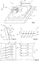
- the figure 1 is a schematic perspective view of a test station adapted to the implementation of a method of facing a network of elementary optical fiber ends with a corresponding network of guide ends wave of a semiconductor wafer.
- each elementary fiber comprises a core provided with its own sheath.
- the test station 1 comprises, in an orthogonal coordinate system defined by three directions or axes X, Y and Z, a frame 3 on which rests a mobile table 5 whose upper face is parallel to the plane defined by the X and Y directions.
- test station 1 further comprises arms 7 integral with the frame 3 and intended to carry various elements useful for testing an integrated optical circuit of a semiconductor wafer.
- a semiconductor wafer 9 comprising integrated optical circuits to be tested is placed on the upper face of the table 5.
- the ends (not represented) of the waveguides of the integrated optical circuits to be tested are on the side of the upper face 11 of the wafer 9.
- An image acquisition device 13 for example a camera possibly associated with a microscope, is mounted on the end of an arm 7, above the semiconductor wafer 9, so as to obtain images of the upper face 11 of the wafer 9.
- the device 13 is for example adapted to visible light whose length of wave is between about 380 and 780 nm.
- a parallelepipedal glass block 15 in which a bundle of elementary optical fibers 17 arranged in a strip is arranged is mounted at the end of another arm 7.
- the elementary fibers are parallel to each other and distributed according to a not regular.
- the end of the arm 7 carrying the block 15 and / or the table 5 carrying the semiconductor wafer 9 comprises means for moving the end of the arm 7 and the table 5 relative to each other in the X and Y.
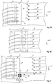
- FIGS 2A and 2B are schematic views respectively of side and bottom of the glass block 15.
- the block 15 consists of two glass plates 15a and 15b glued to each other.
- the plate 15a comprises grooves 19 at its face glued to the plate 15b, for example V-shaped grooves.
- each groove 19 is disposed one of the elementary fibers 17 of the bar.
- the bar comprises five elementary fibers 17, it being understood that a bar may comprise any number of elementary fibers greater than or equal to two.
- the ends of the elementary fibers 17 are aligned and coplanar at the lower face 21 of the block 15.
- the elementary fibers 17 extend so as to be connected, for example to sources of light beams or devices for acquiring light signals. It is considered here that these extensions of the elementary optical fibers 17 are not part of the bar.
- the angle ⁇ between the normal 25 to the lower face 21 of the block 15 and the axis of each fiber 17 of the bar is not zero.
- This angle is chosen according to the coupling networks used, and is for example between 3 and 15 °, for example 8 °. It should be noted that, in the case where the elementary fibers 17 are polarization-maintaining, their orientation in the block 15 is advantageously chosen as a function of the coupling networks used which may be sensitive to the polarization of the light.
- the core of an elementary fiber 17 adapted to transmit light at a wavelength of between 1.3 and 1.5 ⁇ m has a diameter of approximately 7 ⁇ m .
- a light signal of wavelength less than the cutoff wavelength of the elementary fiber is injected into the fiber, diffuse light or escapes from its walls.
- This cut-off wavelength depends on the elementary fiber used and corresponds to the wavelength below which the fiber is no longer monomode.
- An example of an infrared-adapted fiber is the fiber designated by the name SMF28, and this fiber has a cut-off wavelength of 1260 nm.
- the lower face 21 of the block 15 has for example a width of about 2 mm for a length of about 4.5 mm.
- FIGS. 3A to 3C are schematic top views showing the block 15 disposed above the semiconductor wafer 9, these views for example corresponding to images obtained via the image acquisition device 13 of the figure 1 .
- These figures illustrate successive steps of an embodiment of a method of facing the aligned ends of the elementary fibers 17 with aligned ends of waveguides.
- the figure 3A illustrates a preliminary stage of the process.
- the wafer 9 is disposed on the table 5 so that its upper face 11 is substantially parallel to the plane defined by the X and Y directions.
- the semiconductor wafer 9 is also arranged so that the orientation of the alignment of the ends 27 of the waveguides 28 is known, for example so that the coupling networks 27 constituting the ends aligned with waveguides 28 are aligned parallel to the direction X.
- the wafer 9 may comprise a marker, for example a flat on its peripheral edge.
- Block 15 provided with the strip of elementary optical fibers 17 is arranged so that its lower face 21 is vis-à-vis the upper surface 11 of the wafer 9, and substantially parallel thereto.
- the plane of the elementary fiber ends 17 is then substantially parallel to the semiconductor wafer 9 and the axes of the elementary fibers 17 are inclined with respect to the direction Z.
- the block 15 is arranged so that the orientation of the alignment of the ends of the elementary fibers 17 is identical to that of the alignment of the ends 27 of waveguides 28, that is to say that the alignment of the ends of the elementary fibers 17 is parallel to the direction X in this example.
- This is for example achieved by modifying the orientation of the block 15 to make a large edge 30 of its lower surface 21 parallel to the X direction, this edge 30 being visible in top view, parallel to the alignment of the ends of the elementary fibers 17 and serving as orientation reference block 15.
- the projection of the axis of each of these elementary fibers 17 on the semiconductor wafer 9 is then parallel to the Y direction.
- the implementation of these preliminary steps of orientation of the wafer 9 and the block 15 of elementary fibers 17 is within the reach of those skilled in the art.
- a light beam is injected into a, 17a, elementary fibers 17 of the bar.
- the wavelength of the injected light preferably in the form of a laser beam, is chosen outside the range of wavelengths for which the elementary fibers 17 are provided, for example less than the length of the wavelength. cut-off wave of the elementary fiber, from which it follows that this light diffuses from the walls of the elementary fiber 17a.
- the wavelength of the injected light is chosen to obtain a light power diffused from the walls of the elementary fiber 17a that is greater than 1 ⁇ W per centimeter of fiber, preferably greater than 3 ⁇ W per centimeter of fiber.
- This wavelength is furthermore chosen so that the block 15 is at least partially transparent at this wavelength so that the elementary fiber 17a can be distinguished through the block 15. It is then possible to locate the axis 31 of the elementary fiber 17a.
- the wavelength of the injected light is adapted to the image acquisition device 13. In this way, the light diffused by the elementary fiber 17a is visible on the images provided by the device 13 and the axis 31 of the elementary fiber 17a can be located directly on these images.
- the light injected into the elementary fiber 17a may have a wavelength of between 600 and 780 nm, for example 630 nm.
- the fibers are SMF28 fibers and the light signal source provides a laser signal at a wavelength of about 780 to 785 nm, and a power of 10 mW, whereby a light output of about 4 ⁇ W is scattered per centimeter of fiber.
- the semiconductor wafer 9 and the block 15 are then moved relative to each other, in the X direction, until the end 27 of a waveguide 28, referenced hereinafter 27a and 28a respectively, or in the extension of the projection of the axis 31 of the elementary fiber 17a on the upper face 11 of the semiconductor wafer 9.
- the position of the axis 31 of the elementary fiber 17a with respect to the end 27a of the waveguide 28a can be visualized on the images provided by the device 13.
- the observed output signal is a light signal
- its observation is for example carried out by means of an additional elementary optical fiber, one end of which is arranged opposite the corresponding optical output and whose other end is coupled to a photodetector.
- each of the ends of the elementary optical fibers 17 is opposite a corresponding end of the waveguide 28. It can then be realized, as has been previously described, for a single fiber and a single waveguide. wave, a fine adjustment by moving the block 15 and the slice 9 relative to each other so as to maximize the value of a corresponding output signal. The test phase can then begin.
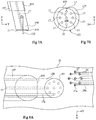
- FIG 4 is a view similar to that of FIGS. 3A to 3C and illustrates an alternative embodiment of the method described above.
- a mark 33 is present on the upper surface 11 of the semiconductor wafer 9.
- the distance x0 in the X direction between the mark 33 and the end 27a of the waveguide 28a is known.
- the mark 33 consists of four squares 35 arranged to define a cross 37, one arm is parallel to the X direction and the other arm is parallel to the Y direction.
- the block 15 and the table 5 are moved relative to each other in the direction X to align the mark 33, in this example the reference arm 33 parallel to the direction Y, in the extension of the projection of the axis 31 of the elementary fiber 17a on the semiconductor wafer 9.
- the block 15 and the wafer 9 are then moved relative to each other in the Y direction until the edge 30 of the block 15 is at the above the mark 33, that is to say above the reference arm 33 parallel to the X direction in this example.
- the figure 4 represents the position of the block 15 above the slice 9 after these steps.
- the block 15 and the semiconductor wafer 9 are then moved relative to each other in the X direction of the known distance x0, the end 27a of the waveguide 28a then being aligned in the extension of the projection of the axis 31 on the semiconductor wafer 9.
- the wafer 9 and the block 15 are then moved relative to each other in the Y direction in the manner described in connection with FIG. figure 3C , until the end of the elementary fiber 17a is vis-à-vis the end 27a of the waveguide 28a.
- the distance y0 of the last displacement Y is stored so that, in a subsequent implementation of the method, after the block 15 has been aligned with the mark 33 as shown in FIG. figure 4 , just move block 15 and the slice 9 relative to each other of the known distance x0 in the direction X and the stored distance y0 in the direction Y to bring the ends of the elementary fibers 17 opposite with the ends 27 of the Waveguides 28.
- the alignment of the mark 33 in the extension of the projection of the axis 31 on the upper face 11 of the semiconductor wafer 9 is generally more accurate than the alignment of the end 27a in this extension.
- the figure 5 is a view similar to that of the figure 3C and illustrates another alternative embodiment of the method described above.
- a vernier 39 graduated in the Y direction is present on the upper surface 11 of the semiconductor wafer 9.
- the method described in connection with the FIGS. 3A to 3C is implemented a first time. Once the stage of the figure 3C completed, the position of the edge 30 of the block 15, and therefore of the elementary fiber bundle 17, is located on the vernier 39.
- the step of the figure 3C is replaced by a step of moving the semiconductor wafer 9 and the block 15 relative to each other in the Y direction until the edge 30 is in the previously marked position. This results in a saving of time for the subsequent implementation of the method.
- the end 27a of the waveguide 28a constitutes a characteristic point of the upper face 11 of the semiconductor wafer 9 and the end of the elementary fiber 17a is directly exposed. with respect to this end 27a of the waveguide 28a, possibly using a reference mark 33.
- the end of the elementary fiber 17a is first brought into view with respect to a characteristic point intermediate, separate from the end 27a of the waveguide 28a, before being placed opposite this end 27a.
- the figure 6 is a view similar to that of the figure 3B and illustrates this alternative embodiment.
- the characteristic point 41 of the upper face 11 of the semiconductor wafer 9 corresponds to an end 41 of an auxiliary waveguide 43.
- the distance x1 in the direction X and the distance y1 in the direction Y which separate this characteristic point 41 of the end 27a of the guide 28a are known.
- the other end 45 of the waveguide 43 is aligned with the characteristic point 41, parallel to the direction X, and the ends 41 and 45 of the waveguide 43 are separated from each other. the other a distance corresponding to that separating two elementary fibers 17 of the bar.
- the semiconductor wafer 9 and the block 15 are then moved relative to each other by the distance x1 in the direction X and the distance y1 in the direction Y to put the end of the elementary fiber 17a vis-à-vis the end 27a of the waveguide 28a.
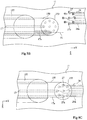
- the Figures 7A and 7B schematically represent another example of a bundle of elementary fibers 17 in the case where the elementary fibers share a same sheath 150, for example glass, and are regularly distributed around a central elemental fiber.
- the Figure 7A is a side view of the beam, a single elementary fiber 17 being represented in dotted line in Figure 7A
- the Figure 7B is a bottom view of an outlet face 153 of the sheath 150 at which the ends of the elementary fibers 17 are flush with the ends 17.
- the elementary fibers 17 are parallel to each other, their ends are coplanar at the face 153 and the axes of the elementary fibers 17 are inclined at an angle ⁇ relative to the normal 155 to this face 153.
- the holding device in which the sheath 150 is disposed is a metal ferrule 157, the end the sheath 150 protruding out of this metal ferrule 157.
- the metal ferrule 157 comprises an orientation mark, in this example a flat 159, so as to be able to orient the elementary fiber bundle 17.
- FIGS. 8A to 8C are schematic top views showing the elementary fiber bundle 17 when the metal ferrule 157 is mounted in place of the block 15 in the test station 1. These figures illustrate successive steps of the method of putting vis-à-vis ends of the elementary fibers 17 with the ends 27 of the waveguides 28 and correspond for example to images obtained via the image acquisition device 13 of the figure 1 . In these figures, only two elementary fibers 17 are shown in dashed lines.
- the figure 8A illustrates the preliminary orientation steps described in relation to the figure 3A applied to the elementary fiber bundle 17 of the Figures 7A and 7B .
- the metal ferrule 157 is arranged so that the ends of the elementary fibers 17 are facing the upper face 11 of the semiconductor wafer 9, the upper face 11 of the wafer 9 being substantially parallel to the face 153 of the sheath 150, so at the plane of the ends of the elementary fibers 17.
- the ends 27 of the waveguides 28 form a network identical to the the network of the ends of the elementary fibers 17 at the face 153 of the sheath 150.
- the semiconductor wafer 9 and the ferrule 157 are arranged so that the network of the ends 27 of the waveguides 28 is oriented in the same way as the the network of the ends of the elementary fibers 17, and that the projection of the axis of each of the elementary fibers 17 on the semiconductor wafer 9 is parallel to the direction Y.
- the flat 159 of the metal ferrule 157 is made parallel to the direction X, and the slice 9 is oriented accordingly as shown in FIG. figure 8A .
- a light beam is injected into an elementary fiber 17a so that light diffuses from its walls, and the axis 31 of the elementary fiber 17a is located at the portion of the sheath 150 protruding out of the ferrule 157.
- the semiconductor wafer 9 and the elementary fiber bundle 17 are then moved relative to each other, in the X direction, until the end 27a of a waveguide 28a is in the extension of the projection of the axis 31 on the upper face 11 of the semiconductor wafer 9.
- the position of the end 27a of the waveguide 28a in the network of the ends 27 of the waveguides 28 corresponds to that of the end of the fiber 17a in the network of the ends of the elementary fibers 17.
- Steps described in relation to the FIGS. 3A to 3C , 4 to 6 and 8A to 8C can be implemented automatically by the test station 1 represented in figure 1 .
- the arm 7 adapted to carry the holding device 15 or 157 of the elementary fiber bundle 17 and / or the table 5 adapted to carry the semiconductor wafer 9 comprise displacement devices (not shown), for example motors stepwise or cylinders, to move the end of the arm 7 and the table 5 relative to each other in the X and Y directions.
- the test station 1 further comprises an image processing device (not shown).
- This image processing device is adapted to locate, thanks to the light diffused by the walls of the elementary fiber 17a, the axis 31 of this elementary fiber 17a on the images supplied by the image acquisition device 13.
- the image processing device is also adapted to identify the position of a characteristic point 41 or 27a, and possibly of the mark 33, on these images.
- the test station 1 also comprises a computing device (not shown) adapted to determine and supply, from the various positions identified and provided by the image processing device and possibly from the knowledge of the distances x0, y0, x1 and y1, control signals of the moving devices of the table 5 and the arm 7 carrying the holding device 15 or 157 of the elementary fiber bundle 17.
- a computing device (not shown) adapted to determine and supply, from the various positions identified and provided by the image processing device and possibly from the knowledge of the distances x0, y0, x1 and y1, control signals of the moving devices of the table 5 and the arm 7 carrying the holding device 15 or 157 of the elementary fiber bundle 17.
- test station 1 may comprise a signal acquisition and processing device (not shown).
- the light and / or electrical signals acquired by this device are processed to identify the moment when the end of the elementary fiber 17a is vis-à-vis the characteristic point 41 or 27a.
- the signal acquisition and processing device provides, possibly via the computing device, control signals for the devices for moving the table 5 and the arm 7 carrying the holding device 15 or 157 of the fiber bundle.
- the computing device, the image processing device, the image acquisition device and, if appropriate, the signal acquisition and processing device each comprise a dedicated circuit or a circuit comprising a microprocessor associated with an instruction memory in which are stored instructions which, when read by the microprocessor, allow the implementation of the functions associated with this device.
- a microprocessor and an instruction memory may be shared by the computing device, the image processing device and / or the signal acquisition and processing device.
- test station 1 allows the automatic implementation of at least some of the steps of the alignment method described above, in particular the step of aligning a characteristic point 41 or 27a of the semiconductor wafer 9 in FIG. the extension of the projection of the axis 31 of the elementary fiber 17a on the semiconductor wafer 9.
- integrated optical circuit covers integrated circuits comprising only optical components, optoelectronic integrated circuits, and more generally integrated circuits comprising at least one integrated optical portion connected to at least one optical input of the circuit.
- the image acquisition device can be oriented so that its optical axis is inclined with respect to the direction Z, for example so that this optical axis is substantially orthogonal to the axis 31 of the fiber 17a.
Landscapes
- Physics & Mathematics (AREA)
- General Physics & Mathematics (AREA)
- Optics & Photonics (AREA)
- Engineering & Computer Science (AREA)
- Microelectronics & Electronic Packaging (AREA)
- Optical Couplings Of Light Guides (AREA)
Claims (14)
- Verfahren zum Anordnen eines Netzwerks koplanarer Enden von Lichtwellenleitern bzw. optischen Fasern (17, 17a) eines Bündels paralleler Fasern, das bezüglich der Normalen zur Ebene der Faserenden geneigt ist, gegenüber einem entsprechenden Netzwerk von Enden (27, 27a) von Wellenleitern (28, 28a) eines Halbleiterwafers (9), wobei das Faserbündel und der Wafer in ersten und zweiten orthogonalen Richtungen (X, Y) zueinander versetzbar sind, wobei das Verfahren die folgenden aufeinanderfolgenden Schritte aufweist:a) Anordnen des Wafers, so dass die Oberseite des Wafers im Wesentlichen parallel zu einer durch die erste und zweite Richtung definierten Ebene ist, und Anordnen des Faserbündels über dem Wafer (9), so dass die Endnetzwerke die gleiche Ausrichtung in Bezug auf die erste und zweite Richtung aufweisen und die Projektion der Achse (31) jeder der Fasern (17, 17a) auf dem Wafer (9) parallel zur zweiten Richtung (Y) ist;b) Einführen in eine (17a) der Fasern (17) eines Lichtstrahls mit einer Wellenlänge so dass Licht von den Seitenwänden der Faser (17a) mit einer Leistung von mehr als 1 µW, vorzugsweise mehr als 3 µW, pro Faserzentimeter gestreut wird, Positionieren der Faserachse (31) basierend auf dem gestreuten Licht von den Seitenwänden der Faser, und Versetzen des Faserbündels und des Wafers (9) zueinander in die erste Richtung (X), um einen charakteristischen Punkt (41, 27a) des Wafers (9) mit einer Linie der Projektion der Achse (31) der Faser (17a) auf dem Wafer (9) auszurichten; undc) Versetzen des Faserbündels und des Wafers (9) relativ zueinander, bis das Ende der Faser (17a) gegenüber einem entsprechenden Ende (27a) eines Wellenleiters (28a) angeordnet ist.
- Verfahren nach Anspruch 1, wobei der charakteristische Punkt (27a) dem Ende (27a) eines Wellenleiters (28a) entspricht, wobei der Schritt c) einen Schritt c1) des Versetzens des Wafers (9) und des Faserbündels relativ zueinander in der zweiten Richtung (Y) aufweist, bis das Ende der Faser (17a) gegenüber dem Punkt (27a) angeordnet ist.
- Verfahren nach Anspruch 1, wobei der charakteristische Punkt (41) einem Ende eines Hilfs-Wellenleiters (43) entspricht und die Position des charakteristischen Punktes (41) relativ zu dem Ende (27a) eines Wellenleiters (28a) bekannt und wobei Schritt c) nacheinander Folgendes aufweist:einen Schritt c1) des Versetzens des Wafers (9) und des Faserbündels relativ zueinander in die zweite Richtung (Y), bis das Ende der Faser (17a) oberhalb des charakteristischen Punktes (41) liegt; undeinen Schritt c2) des Versetzens des Wafers (9) und des Faserbündels relativ zueinander basierend auf der bekannten Position des Punktes (41) relativ zu dem Ende (27a) eines Wellenleiters (28a).
- Verfahren nach Anspruch 2 oder 3, wobei im Schritt c1) das Versetzen gestoppt wird, wenn die auf der Höhe des charakteristischen Punktes (27a, 41) empfangene Lichtmenge maximal ist.
- Verfahren nach einem der Ansprüche 2 bis 4, wobei der Wafer (9) einen Mess-Nonius (39) in der zweiten Richtung (Y) aufweiwst, wobei das Verfahren ferner Folgendes saufweist:am Ende von Schritt c1), Lokalisieren der Position des Faserbündels auf dem Nonius (39); undwährend einer nachfolgenden Ausrichtung der Enden der Fasern (17) auf den Enden (27) der Wellenleiter (28), Ausführen der Schritte a) und b) und dann eines Schrittes des Versetzens des Wafers (9) und des Faserbündels relativ zueinander in der zweiten Richtung (Y) bis zur lokalisierten Position.
- Verfahren nach einem der Ansprüche 1 bis 5, wobei im Schritt c) ein Lichtstrahl mit einer an die Faser (17a) angepassten Wellenlänge in die Faser (17a) eingeführt wird.
- Verfahren nach einem der Ansprüche 1 bis 6, wobei die Fasern (17) und die Wellenleiter (28) in der Lage sind, ein Lichtsignal mit einer Wellenlänge im Bereich von 1,3 bis 1,5 µm zu übertragen.
- Verfahren nach Anspruch 7, wobei im Schritt b) die Wellenlänge des Strahls im Bereich von 600 bis 780 nm liegt.
- Verfahren nach einem der Ansprüche 1 bis 8, wobei die Fasern (17) eine gleiche Umhüllung (150) teilen.
- Verfahren nach einem der Ansprüche 1 bis 8, wobei die Fasern (17) in einem Stab angeordnet sind.
- Verfahren nach einem der Ansprüche 1 bis 10, wobei das Faserbündel in einer Haltevorrichtung (15, 157) angeordnet ist, die eine Orientierungsmarke (30, 159) aufweist, wobei der Schritt a) das Ausrichten der Orientierungsmarke mit der ersten Richtung (X) aufweist.
- Verfahren nach einem der Ansprüche 1 bis 11, wobei im Schritt a) die Ebene der Enden der optischen Fasern (17) parallel zur ersten und zweiten Richtung ausgerichtet wird.
- Prüfstation (1), die in der Lage ist, das Verfahren nach einem der Ansprüche 1 bis 12 durchzuführen, wobei die Prüfstation (1) Folgendes aufweist:einen Arm (7), der die Haltevorrichtung (15, 157) des Faserbündels (17) tragen kann, und einen Tisch (5), der einen Halbleiterwafer (9) tragen kann,der Arm (7) und/oder der Tisch (5) weisen Versatzvorrichtungen zum Versetzen des Endes des Arms (7) und des Tisches (5) relativ zueinander in einer ersten und zweiten orthogonalen Richtung (X, Y) auf, undMittel, die in der Lage sind, in eine (17a) der Fasern (17) einen Lichtstrahl mit einer Wellenlänge einzubringen, so dass Licht von den Seitenwänden der Faser (17a) mit einer Leistung von mehr als 1 µW, vorzugsweise mehr als 3 µW, pro Faserzentimeter gestreut wird.
- Prüfstation nach Anspruch 13, wobei Schritt b) nach Anspruch 1 in automatischer Weist implementiert wird.
Applications Claiming Priority (1)
| Application Number | Priority Date | Filing Date | Title |
|---|---|---|---|
| FR1752269A FR3064077B1 (fr) | 2017-03-20 | 2017-03-20 | Procede de mise en vis-a-vis des extremites de fibres optiques avec des extremites de guides d'onde |
Publications (2)
| Publication Number | Publication Date |
|---|---|
| EP3379308A1 EP3379308A1 (de) | 2018-09-26 |
| EP3379308B1 true EP3379308B1 (de) | 2019-10-30 |
Family
ID=59031128
Family Applications (1)
| Application Number | Title | Priority Date | Filing Date |
|---|---|---|---|
| EP18161597.2A Active EP3379308B1 (de) | 2017-03-20 | 2018-03-13 | Verfahren zur gegenüberstellung der extremitäten von optischen fasern und von lichtwellenleitern und eine prüfstation, die zur durchführung des verfahrens geignet ist |
Country Status (3)
| Country | Link |
|---|---|
| US (1) | US10330865B2 (de) |
| EP (1) | EP3379308B1 (de) |
| FR (1) | FR3064077B1 (de) |
Families Citing this family (3)
| Publication number | Priority date | Publication date | Assignee | Title |
|---|---|---|---|---|
| US12092658B2 (en) * | 2021-08-18 | 2024-09-17 | Mpi Corporation | Optical detection system and alignment method for a predetermined target object |
| US12687672B2 (en) | 2023-06-30 | 2026-07-21 | IonQ Inc. | Alignment of adiabatic optical interfaces |
| JP2026525184A (ja) * | 2023-06-30 | 2026-07-29 | イオンキュー インコーポレイテッド | 光活性化リソグラフィを用いて固定された断熱光学インターフェース |
Family Cites Families (10)
| Publication number | Priority date | Publication date | Assignee | Title |
|---|---|---|---|---|
| US5770125A (en) * | 1995-11-27 | 1998-06-23 | Mentor Corporation | Haptic attachment system for intraocular lenses using diode laser |
| JP3401420B2 (ja) * | 1997-11-12 | 2003-04-28 | 沖電気工業株式会社 | 光フィルタの位置合わせ装置および光フィルタの位置合わせ方法 |
| GB2374156A (en) * | 2001-04-02 | 2002-10-09 | Kamelian Ltd | Aligning array of optical fibres with waveguides of optical device |
| US6618514B1 (en) * | 2001-10-11 | 2003-09-09 | Lightwave Microsystems Corporation | Passive pigtail attachment apparatus and method for planar lightwave circuits |
| US7184626B1 (en) | 2003-04-07 | 2007-02-27 | Luxtera, Inc | Wafer-level testing of optical and optoelectronic chips |
| US7263256B2 (en) * | 2004-04-02 | 2007-08-28 | Samsung Electronics Co., Ltd. | Optical connection block, optical module, and optical axis alignment method using the same |
| JP6082523B2 (ja) * | 2011-08-01 | 2017-02-15 | 古河電気工業株式会社 | マルチコアファイバの接続方法、マルチコアファイバ、マルチコアファイバの製造方法 |
| US8620123B2 (en) * | 2012-02-13 | 2013-12-31 | Corning Cable Systems Llc | Visual tracer system for fiber optic cable |
| US9372304B2 (en) * | 2013-03-28 | 2016-06-21 | Ofs Fitel, Llc | Apparatus for alignment of a multicore fiber in a multifiber connector and method of using same |
| US9213134B2 (en) * | 2013-08-06 | 2015-12-15 | Verizon Patent And Licensing Inc. | Alignment for splicing multi-core optical fibers |
-
2017
- 2017-03-20 FR FR1752269A patent/FR3064077B1/fr not_active Expired - Fee Related
-
2018
- 2018-03-13 EP EP18161597.2A patent/EP3379308B1/de active Active
- 2018-03-19 US US15/924,987 patent/US10330865B2/en active Active
Non-Patent Citations (1)
| Title |
|---|
| None * |
Also Published As
| Publication number | Publication date |
|---|---|
| US20180267244A1 (en) | 2018-09-20 |
| FR3064077B1 (fr) | 2019-08-09 |
| EP3379308A1 (de) | 2018-09-26 |
| US10330865B2 (en) | 2019-06-25 |
| FR3064077A1 (fr) | 2018-09-21 |
Similar Documents
| Publication | Publication Date | Title |
|---|---|---|
| EP2198273B1 (de) | Modulares bildgebungssystem und bildgebungsverfahren | |
| EP0825464B1 (de) | Verfahren zur Herstellung und Montage von einem kollektiven optischen Kopplungselement am Ende eines Bündels von mehreren Monomodenfasern | |
| EP2805133B1 (de) | Geführter optische router, faseroptisches interferometer mit einem solchen optischer router und verfahren für geführtes optisches routing | |
| FR3049719B1 (fr) | Dispositifs et methodes de transport et de controle de faisceaux lumineux pour l'imagerie endo-microscopique sans lentille | |
| FR2947347A1 (fr) | Structure et procede d'alignement d'une fibre optique et d'un guide d'ondes submicronique | |
| FR3064077B1 (fr) | Procede de mise en vis-a-vis des extremites de fibres optiques avec des extremites de guides d'onde | |
| EP3234666A1 (de) | Vorrichtung zum transport und zur steuerung der lichtimpulse zur linsenlosen endomikroskopischen bildgebung | |
| WO2020254760A1 (fr) | Procédé de fixation d'une fibre optique monomode et d'une fibre optique multimode, équipement de couplage optique | |
| FR3077887A1 (fr) | Puce optoelectronique et procede de test de circuits photoniques d'une telle puce | |
| FR2937426A1 (fr) | Structure et procede d'alignement d'une fibre optique sur un guide d'ondes optique | |
| FR2745082A1 (fr) | Procede et dispositif de mesure de la dispersion de polarisation d'une fibre optique | |
| FR3077888A1 (fr) | Puce optoelectronique et procede de test de circuits photoniques d'une telle puce | |
| FR2768814A1 (fr) | Procede et dispositif optiques d'analyse de surface d'onde | |
| EP0840158B1 (de) | Vorrichtung zur Bestimmung von Phasenfehlern elektromagnetischer Wellen | |
| EP4302148B1 (de) | System zur kompensation der verzerrung einer wellenfront eines einfallenden lichtstrahls | |
| EP0018873A1 (de) | Kompakte optische Koppelungsvorrichtung und solch eine Vorrichtung enthaltender interferometrischer Gyrometer mit einer optischen Faser | |
| EP0077259B1 (de) | Verfahren und Vorrichtung zum Messen des effektiven Diameters des Leitmodus in einer monomoden optischen Faser | |
| EP0384828B1 (de) | Anordnung zur Kontrolle der modalen Ausrichtung optischer Fasern | |
| FR3139626A1 (fr) | Dispositif de mesure de front d'onde optique et procédé de mesure associé | |
| EP1910797B1 (de) | Verfahren und einrichtung zur messung der konzentrizität eines optischen faserkerns | |
| FR3143111A1 (fr) | Dispositif de mesure d’une grandeur physique | |
| EP0926529B1 (de) | Verfahren und Vorrichtung zur automatischen Positionskorrektur von optischen Elementen in einem optischen Aufbau | |
| EP4372435B1 (de) | Photonischer chip und infrarot-abbildungssystem mit einem solchen photonischen chip | |
| FR2584811A1 (fr) | Dispositif de mesure de deformations d'un corps, notamment d'une maquette en soufflerie aerodynamique | |
| EP0503558B1 (de) | Einrichtung zur Sichtbarmachung des Kerns einer Glasfaser |
Legal Events
| Date | Code | Title | Description |
|---|---|---|---|
| PUAI | Public reference made under article 153(3) epc to a published international application that has entered the european phase |
Free format text: ORIGINAL CODE: 0009012 |
|
| STAA | Information on the status of an ep patent application or granted ep patent |
Free format text: STATUS: REQUEST FOR EXAMINATION WAS MADE |
|
| 17P | Request for examination filed |
Effective date: 20180313 |
|
| AK | Designated contracting states |
Kind code of ref document: A1 Designated state(s): AL AT BE BG CH CY CZ DE DK EE ES FI FR GB GR HR HU IE IS IT LI LT LU LV MC MK MT NL NO PL PT RO RS SE SI SK SM TR |
|
| AX | Request for extension of the european patent |
Extension state: BA ME |
|
| STAA | Information on the status of an ep patent application or granted ep patent |
Free format text: STATUS: EXAMINATION IS IN PROGRESS |
|
| 17Q | First examination report despatched |
Effective date: 20181109 |
|
| RIC1 | Information provided on ipc code assigned before grant |
Ipc: G02B 6/36 20060101ALN20190424BHEP Ipc: G02B 6/30 20060101AFI20190424BHEP Ipc: G02B 6/42 20060101ALI20190424BHEP |
|
| RIC1 | Information provided on ipc code assigned before grant |
Ipc: G02B 6/30 20060101AFI20190605BHEP Ipc: G02B 6/36 20060101ALN20190605BHEP Ipc: G02B 6/42 20060101ALI20190605BHEP |
|
| GRAP | Despatch of communication of intention to grant a patent |
Free format text: ORIGINAL CODE: EPIDOSNIGR1 |
|
| STAA | Information on the status of an ep patent application or granted ep patent |
Free format text: STATUS: GRANT OF PATENT IS INTENDED |
|
| INTG | Intention to grant announced |
Effective date: 20190711 |
|
| GRAJ | Information related to disapproval of communication of intention to grant by the applicant or resumption of examination proceedings by the epo deleted |
Free format text: ORIGINAL CODE: EPIDOSDIGR1 |
|
| STAA | Information on the status of an ep patent application or granted ep patent |
Free format text: STATUS: EXAMINATION IS IN PROGRESS |
|
| GRAR | Information related to intention to grant a patent recorded |
Free format text: ORIGINAL CODE: EPIDOSNIGR71 |
|
| GRAS | Grant fee paid |
Free format text: ORIGINAL CODE: EPIDOSNIGR3 |
|
| STAA | Information on the status of an ep patent application or granted ep patent |
Free format text: STATUS: GRANT OF PATENT IS INTENDED |
|
| GRAA | (expected) grant |
Free format text: ORIGINAL CODE: 0009210 |
|
| STAA | Information on the status of an ep patent application or granted ep patent |
Free format text: STATUS: THE PATENT HAS BEEN GRANTED |
|
| INTC | Intention to grant announced (deleted) | ||
| RIC1 | Information provided on ipc code assigned before grant |
Ipc: G02B 6/30 20060101AFI20190906BHEP Ipc: G02B 6/36 20060101ALN20190906BHEP Ipc: G02B 6/42 20060101ALI20190906BHEP |
|
| RIC1 | Information provided on ipc code assigned before grant |
Ipc: G02B 6/42 20060101ALI20190916BHEP Ipc: G02B 6/36 20060101ALN20190916BHEP Ipc: G02B 6/30 20060101AFI20190916BHEP |
|
| AK | Designated contracting states |
Kind code of ref document: B1 Designated state(s): AL AT BE BG CH CY CZ DE DK EE ES FI FR GB GR HR HU IE IS IT LI LT LU LV MC MK MT NL NO PL PT RO RS SE SI SK SM TR |
|
| INTG | Intention to grant announced |
Effective date: 20190923 |
|
| REG | Reference to a national code |
Ref country code: GB Ref legal event code: FG4D Free format text: NOT ENGLISH |
|
| RIC1 | Information provided on ipc code assigned before grant |
Ipc: G02B 6/30 20060101AFI20190923BHEP Ipc: G02B 6/36 20060101ALN20190923BHEP Ipc: G02B 6/42 20060101ALI20190923BHEP |
|
| REG | Reference to a national code |
Ref country code: CH Ref legal event code: EP |
|
| REG | Reference to a national code |
Ref country code: AT Ref legal event code: REF Ref document number: 1196771 Country of ref document: AT Kind code of ref document: T Effective date: 20191115 |
|
| REG | Reference to a national code |
Ref country code: DE Ref legal event code: R096 Ref document number: 602018001003 Country of ref document: DE |
|
| REG | Reference to a national code |
Ref country code: IE Ref legal event code: FG4D Free format text: LANGUAGE OF EP DOCUMENT: FRENCH |
|
| REG | Reference to a national code |
Ref country code: LT Ref legal event code: MG4D |
|
| PG25 | Lapsed in a contracting state [announced via postgrant information from national office to epo] |
Ref country code: NO Free format text: LAPSE BECAUSE OF FAILURE TO SUBMIT A TRANSLATION OF THE DESCRIPTION OR TO PAY THE FEE WITHIN THE PRESCRIBED TIME-LIMIT Effective date: 20200130 Ref country code: PL Free format text: LAPSE BECAUSE OF FAILURE TO SUBMIT A TRANSLATION OF THE DESCRIPTION OR TO PAY THE FEE WITHIN THE PRESCRIBED TIME-LIMIT Effective date: 20191030 Ref country code: GR Free format text: LAPSE BECAUSE OF FAILURE TO SUBMIT A TRANSLATION OF THE DESCRIPTION OR TO PAY THE FEE WITHIN THE PRESCRIBED TIME-LIMIT Effective date: 20200131 Ref country code: FI Free format text: LAPSE BECAUSE OF FAILURE TO SUBMIT A TRANSLATION OF THE DESCRIPTION OR TO PAY THE FEE WITHIN THE PRESCRIBED TIME-LIMIT Effective date: 20191030 Ref country code: BG Free format text: LAPSE BECAUSE OF FAILURE TO SUBMIT A TRANSLATION OF THE DESCRIPTION OR TO PAY THE FEE WITHIN THE PRESCRIBED TIME-LIMIT Effective date: 20200130 Ref country code: LT Free format text: LAPSE BECAUSE OF FAILURE TO SUBMIT A TRANSLATION OF THE DESCRIPTION OR TO PAY THE FEE WITHIN THE PRESCRIBED TIME-LIMIT Effective date: 20191030 Ref country code: SE Free format text: LAPSE BECAUSE OF FAILURE TO SUBMIT A TRANSLATION OF THE DESCRIPTION OR TO PAY THE FEE WITHIN THE PRESCRIBED TIME-LIMIT Effective date: 20191030 Ref country code: LV Free format text: LAPSE BECAUSE OF FAILURE TO SUBMIT A TRANSLATION OF THE DESCRIPTION OR TO PAY THE FEE WITHIN THE PRESCRIBED TIME-LIMIT Effective date: 20191030 Ref country code: PT Free format text: LAPSE BECAUSE OF FAILURE TO SUBMIT A TRANSLATION OF THE DESCRIPTION OR TO PAY THE FEE WITHIN THE PRESCRIBED TIME-LIMIT Effective date: 20200302 Ref country code: NL Free format text: LAPSE BECAUSE OF FAILURE TO SUBMIT A TRANSLATION OF THE DESCRIPTION OR TO PAY THE FEE WITHIN THE PRESCRIBED TIME-LIMIT Effective date: 20191030 |
|
| REG | Reference to a national code |
Ref country code: NL Ref legal event code: MP Effective date: 20191030 |
|
| PG25 | Lapsed in a contracting state [announced via postgrant information from national office to epo] |
Ref country code: IS Free format text: LAPSE BECAUSE OF FAILURE TO SUBMIT A TRANSLATION OF THE DESCRIPTION OR TO PAY THE FEE WITHIN THE PRESCRIBED TIME-LIMIT Effective date: 20200229 Ref country code: HR Free format text: LAPSE BECAUSE OF FAILURE TO SUBMIT A TRANSLATION OF THE DESCRIPTION OR TO PAY THE FEE WITHIN THE PRESCRIBED TIME-LIMIT Effective date: 20191030 Ref country code: RS Free format text: LAPSE BECAUSE OF FAILURE TO SUBMIT A TRANSLATION OF THE DESCRIPTION OR TO PAY THE FEE WITHIN THE PRESCRIBED TIME-LIMIT Effective date: 20191030 |
|
| PG25 | Lapsed in a contracting state [announced via postgrant information from national office to epo] |
Ref country code: AL Free format text: LAPSE BECAUSE OF FAILURE TO SUBMIT A TRANSLATION OF THE DESCRIPTION OR TO PAY THE FEE WITHIN THE PRESCRIBED TIME-LIMIT Effective date: 20191030 |
|
| PG25 | Lapsed in a contracting state [announced via postgrant information from national office to epo] |
Ref country code: ES Free format text: LAPSE BECAUSE OF FAILURE TO SUBMIT A TRANSLATION OF THE DESCRIPTION OR TO PAY THE FEE WITHIN THE PRESCRIBED TIME-LIMIT Effective date: 20191030 Ref country code: DK Free format text: LAPSE BECAUSE OF FAILURE TO SUBMIT A TRANSLATION OF THE DESCRIPTION OR TO PAY THE FEE WITHIN THE PRESCRIBED TIME-LIMIT Effective date: 20191030 Ref country code: EE Free format text: LAPSE BECAUSE OF FAILURE TO SUBMIT A TRANSLATION OF THE DESCRIPTION OR TO PAY THE FEE WITHIN THE PRESCRIBED TIME-LIMIT Effective date: 20191030 Ref country code: RO Free format text: LAPSE BECAUSE OF FAILURE TO SUBMIT A TRANSLATION OF THE DESCRIPTION OR TO PAY THE FEE WITHIN THE PRESCRIBED TIME-LIMIT Effective date: 20191030 Ref country code: CZ Free format text: LAPSE BECAUSE OF FAILURE TO SUBMIT A TRANSLATION OF THE DESCRIPTION OR TO PAY THE FEE WITHIN THE PRESCRIBED TIME-LIMIT Effective date: 20191030 |
|
| REG | Reference to a national code |
Ref country code: DE Ref legal event code: R097 Ref document number: 602018001003 Country of ref document: DE |
|
| REG | Reference to a national code |
Ref country code: AT Ref legal event code: MK05 Ref document number: 1196771 Country of ref document: AT Kind code of ref document: T Effective date: 20191030 |
|
| PG25 | Lapsed in a contracting state [announced via postgrant information from national office to epo] |
Ref country code: IT Free format text: LAPSE BECAUSE OF FAILURE TO SUBMIT A TRANSLATION OF THE DESCRIPTION OR TO PAY THE FEE WITHIN THE PRESCRIBED TIME-LIMIT Effective date: 20191030 Ref country code: SM Free format text: LAPSE BECAUSE OF FAILURE TO SUBMIT A TRANSLATION OF THE DESCRIPTION OR TO PAY THE FEE WITHIN THE PRESCRIBED TIME-LIMIT Effective date: 20191030 Ref country code: SK Free format text: LAPSE BECAUSE OF FAILURE TO SUBMIT A TRANSLATION OF THE DESCRIPTION OR TO PAY THE FEE WITHIN THE PRESCRIBED TIME-LIMIT Effective date: 20191030 |
|
| PLBE | No opposition filed within time limit |
Free format text: ORIGINAL CODE: 0009261 |
|
| STAA | Information on the status of an ep patent application or granted ep patent |
Free format text: STATUS: NO OPPOSITION FILED WITHIN TIME LIMIT |
|
| 26N | No opposition filed |
Effective date: 20200731 |
|
| PG25 | Lapsed in a contracting state [announced via postgrant information from national office to epo] |
Ref country code: MC Free format text: LAPSE BECAUSE OF FAILURE TO SUBMIT A TRANSLATION OF THE DESCRIPTION OR TO PAY THE FEE WITHIN THE PRESCRIBED TIME-LIMIT Effective date: 20191030 |
|
| PG25 | Lapsed in a contracting state [announced via postgrant information from national office to epo] |
Ref country code: AT Free format text: LAPSE BECAUSE OF FAILURE TO SUBMIT A TRANSLATION OF THE DESCRIPTION OR TO PAY THE FEE WITHIN THE PRESCRIBED TIME-LIMIT Effective date: 20191030 Ref country code: SI Free format text: LAPSE BECAUSE OF FAILURE TO SUBMIT A TRANSLATION OF THE DESCRIPTION OR TO PAY THE FEE WITHIN THE PRESCRIBED TIME-LIMIT Effective date: 20191030 |
|
| REG | Reference to a national code |
Ref country code: BE Ref legal event code: MM Effective date: 20200331 |
|
| PG25 | Lapsed in a contracting state [announced via postgrant information from national office to epo] |
Ref country code: LU Free format text: LAPSE BECAUSE OF NON-PAYMENT OF DUE FEES Effective date: 20200313 |
|
| PG25 | Lapsed in a contracting state [announced via postgrant information from national office to epo] |
Ref country code: IE Free format text: LAPSE BECAUSE OF NON-PAYMENT OF DUE FEES Effective date: 20200313 |
|
| PG25 | Lapsed in a contracting state [announced via postgrant information from national office to epo] |
Ref country code: BE Free format text: LAPSE BECAUSE OF NON-PAYMENT OF DUE FEES Effective date: 20200331 |
|
| REG | Reference to a national code |
Ref country code: CH Ref legal event code: PL |
|
| PG25 | Lapsed in a contracting state [announced via postgrant information from national office to epo] |
Ref country code: CH Free format text: LAPSE BECAUSE OF NON-PAYMENT OF DUE FEES Effective date: 20210331 Ref country code: LI Free format text: LAPSE BECAUSE OF NON-PAYMENT OF DUE FEES Effective date: 20210331 |
|
| PG25 | Lapsed in a contracting state [announced via postgrant information from national office to epo] |
Ref country code: TR Free format text: LAPSE BECAUSE OF FAILURE TO SUBMIT A TRANSLATION OF THE DESCRIPTION OR TO PAY THE FEE WITHIN THE PRESCRIBED TIME-LIMIT Effective date: 20191030 Ref country code: MT Free format text: LAPSE BECAUSE OF FAILURE TO SUBMIT A TRANSLATION OF THE DESCRIPTION OR TO PAY THE FEE WITHIN THE PRESCRIBED TIME-LIMIT Effective date: 20191030 Ref country code: CY Free format text: LAPSE BECAUSE OF FAILURE TO SUBMIT A TRANSLATION OF THE DESCRIPTION OR TO PAY THE FEE WITHIN THE PRESCRIBED TIME-LIMIT Effective date: 20191030 |
|
| PG25 | Lapsed in a contracting state [announced via postgrant information from national office to epo] |
Ref country code: MK Free format text: LAPSE BECAUSE OF FAILURE TO SUBMIT A TRANSLATION OF THE DESCRIPTION OR TO PAY THE FEE WITHIN THE PRESCRIBED TIME-LIMIT Effective date: 20191030 |
|
| PGFP | Annual fee paid to national office [announced via postgrant information from national office to epo] |
Ref country code: GB Payment date: 20260324 Year of fee payment: 9 |
|
| PGFP | Annual fee paid to national office [announced via postgrant information from national office to epo] |
Ref country code: DE Payment date: 20260320 Year of fee payment: 9 |
|
| PGFP | Annual fee paid to national office [announced via postgrant information from national office to epo] |
Ref country code: FR Payment date: 20260324 Year of fee payment: 9 |