EP3379557A1 - Microscope électronique à transmission et à balayage et procédé d'acquisition à haut rendement des images de la distribution de l'angle de diffusion d'électrons - Google Patents
Microscope électronique à transmission et à balayage et procédé d'acquisition à haut rendement des images de la distribution de l'angle de diffusion d'électrons Download PDFInfo
- Publication number
- EP3379557A1 EP3379557A1 EP17000450.1A EP17000450A EP3379557A1 EP 3379557 A1 EP3379557 A1 EP 3379557A1 EP 17000450 A EP17000450 A EP 17000450A EP 3379557 A1 EP3379557 A1 EP 3379557A1
- Authority
- EP
- European Patent Office
- Prior art keywords
- detector
- electron
- scattering angle
- angle distribution
- electron beam
- Prior art date
- Legal status (The legal status is an assumption and is not a legal conclusion. Google has not performed a legal analysis and makes no representation as to the accuracy of the status listed.)
- Withdrawn
Links
- 238000009826 distribution Methods 0.000 title claims abstract description 75
- 238000001803 electron scattering Methods 0.000 title claims abstract description 54
- 238000000034 method Methods 0.000 title claims abstract description 26
- 230000005540 biological transmission Effects 0.000 title claims description 14
- 238000010894 electron beam technology Methods 0.000 claims abstract description 56
- 238000002524 electron diffraction data Methods 0.000 claims description 11
- 238000012805 post-processing Methods 0.000 claims description 3
- 230000010354 integration Effects 0.000 claims 1
- 239000000463 material Substances 0.000 abstract description 5
- 239000002086 nanomaterial Substances 0.000 abstract description 2
- 230000003287 optical effect Effects 0.000 description 18
- 238000002003 electron diffraction Methods 0.000 description 10
- 238000011144 upstream manufacturing Methods 0.000 description 6
- 238000002441 X-ray diffraction Methods 0.000 description 4
- 238000010586 diagram Methods 0.000 description 4
- 230000000694 effects Effects 0.000 description 4
- 239000002245 particle Substances 0.000 description 4
- 230000035945 sensitivity Effects 0.000 description 4
- 238000004458 analytical method Methods 0.000 description 2
- 230000008901 benefit Effects 0.000 description 2
- 239000013078 crystal Substances 0.000 description 2
- 230000001360 synchronised effect Effects 0.000 description 2
- 230000008685 targeting Effects 0.000 description 2
- 238000000333 X-ray scattering Methods 0.000 description 1
- 230000008859 change Effects 0.000 description 1
- 238000001514 detection method Methods 0.000 description 1
- 239000000835 fiber Substances 0.000 description 1
- 238000003384 imaging method Methods 0.000 description 1
- 230000003993 interaction Effects 0.000 description 1
- 238000005259 measurement Methods 0.000 description 1
- 239000002159 nanocrystal Substances 0.000 description 1
- 239000002707 nanocrystalline material Substances 0.000 description 1
- 230000008569 process Effects 0.000 description 1
- 230000001902 propagating effect Effects 0.000 description 1
- 239000011343 solid material Substances 0.000 description 1
- 238000012916 structural analysis Methods 0.000 description 1
Images


Classifications
-
- H—ELECTRICITY
- H01—ELECTRIC ELEMENTS
- H01J—ELECTRIC DISCHARGE TUBES OR DISCHARGE LAMPS
- H01J37/00—Discharge tubes with provision for introducing objects or material to be exposed to the discharge, e.g. for the purpose of examination or processing thereof
- H01J37/26—Electron or ion microscopes; Electron or ion diffraction tubes
- H01J37/28—Electron or ion microscopes; Electron or ion diffraction tubes with scanning beams
-
- G—PHYSICS
- G01—MEASURING; TESTING
- G01N—INVESTIGATING OR ANALYSING MATERIALS BY DETERMINING THEIR CHEMICAL OR PHYSICAL PROPERTIES
- G01N23/00—Investigating or analysing materials by the use of wave or particle radiation, e.g. X-rays or neutrons, not covered by groups G01N3/00 – G01N17/00, G01N21/00 or G01N22/00
- G01N23/20—Investigating or analysing materials by the use of wave or particle radiation, e.g. X-rays or neutrons, not covered by groups G01N3/00 – G01N17/00, G01N21/00 or G01N22/00 by using diffraction of the radiation by the materials, e.g. for investigating crystal structure; by using scattering of the radiation by the materials, e.g. for investigating non-crystalline materials; by using reflection of the radiation by the materials
- G01N23/20058—Measuring diffraction of electrons, e.g. low energy electron diffraction [LEED] method or reflection high energy electron diffraction [RHEED] method
-
- H—ELECTRICITY
- H01—ELECTRIC ELEMENTS
- H01J—ELECTRIC DISCHARGE TUBES OR DISCHARGE LAMPS
- H01J37/00—Discharge tubes with provision for introducing objects or material to be exposed to the discharge, e.g. for the purpose of examination or processing thereof
- H01J37/02—Details
- H01J37/244—Detectors; Associated components or circuits therefor
-
- H—ELECTRICITY
- H01—ELECTRIC ELEMENTS
- H01J—ELECTRIC DISCHARGE TUBES OR DISCHARGE LAMPS
- H01J2237/00—Discharge tubes exposing object to beam, e.g. for analysis treatment, etching, imaging
- H01J2237/15—Means for deflecting or directing discharge
- H01J2237/1506—Tilting or rocking beam around an axis substantially at an angle to optical axis
-
- H—ELECTRICITY
- H01—ELECTRIC ELEMENTS
- H01J—ELECTRIC DISCHARGE TUBES OR DISCHARGE LAMPS
- H01J2237/00—Discharge tubes exposing object to beam, e.g. for analysis treatment, etching, imaging
- H01J2237/26—Electron or ion microscopes
- H01J2237/28—Scanning microscopes
- H01J2237/2802—Transmission microscopes
-
- H—ELECTRICITY
- H01—ELECTRIC ELEMENTS
- H01J—ELECTRIC DISCHARGE TUBES OR DISCHARGE LAMPS
- H01J2237/00—Discharge tubes exposing object to beam, e.g. for analysis treatment, etching, imaging
- H01J2237/26—Electron or ion microscopes
- H01J2237/28—Scanning microscopes
- H01J2237/2803—Scanning microscopes characterised by the imaging method
- H01J2237/2804—Scattered primary beam
- H01J2237/2805—Elastic scattering
Definitions
- the present invention is a method and device in the field of structural determination of materials using techniques that are suitable for high-throughput structural analysis, and which can be applied to nanoscale structures.
- X-Ray diffraction is a technique providing an average structure, usually of a volume no less than about 1 micrometer cubed.
- XRD X-Ray diffraction
- Electron diffraction has some advantages over XRD for nanocrystalline materials.
- the strength of scattering of electrons from atoms is several orders of magnitude higher than the strength of X-Ray scattering, which makes the ED signal much higher intensity than the XRD signal for small particles.
- ED can happen from a volume as small as 1 nanometer cubed without any of the artifacts seen in XRD patterns from nanocrystals.
- PED Precession Electron Diffraction
- the electron beam To determine the variation in atomic structure or crystal orientation within a specimen, the electron beam must be moved to multiple positions, and an ED or PED pattern must be recorded from each position.
- the quality of the measurement is affected by the quality of the recorded diffraction patterns, and also by the number of positions recorded.
- the number of positions is limited mainly by the recording speed of the camera used for recording the ED patterns, but increasing the recording speed can also reduce the quality of the ED patterns. Therefore, it is critical to select a configuration for recording the ED patterns that optimizes both the recording speed and the detector sensitivity.
- On-axis cameras can also be used for recording PED patterns. These cameras have their own scintillator (instead of the microscope fluorescent screen) usually coupled to the camera sensor using fiber optics (instead of a lens), so they can gather virtually all of the light produced by the scintillator. These cameras are very sensitive, but they can typically read out only 10-100 PED patterns per second.
- the embodiment of the invention is a method and device for high throughput electron scattering angle distribution acquisition from an electron transparent sample.
- the method and device provide for fast analysis of the structure of crystalline and amorphous materials based on fast acquisition of a transmitted signal using one or more detectors.
- the transmitted signal may produce electron diffraction (ED) patterns, precession electron diffraction (PED) patterns or bright field (BF) and dark field (DF) images.
- ED electron diffraction
- PED precession electron diffraction
- BF bright field
- DF dark field
- the device is an electron beam system, preferably a (scanning) transmission electron microscope (STEM) comprising an electron beam source producing a primary electron beam with energy typically up to 300keV propagating along an optical axis. Downstream of the electron beam source follows a condenser lens system for defining the beam shape, size and convergence angle.
- the condenser lens system may be followed by a condenser objective lens system that may comprise Fourier lenses or common condenser objective lenses typically with at least an upper pole piece and a lower pole piece.
- the condenser objective Fourier lenses compared to common condenser objective lenses generate two diffraction images which are positioned before the virtual image generated by the condenser objective Fourier lens.
- the field of the condenser objective Fourier lens upstream of the object generates a finely focused spot from the primary electron beam in the object plane.
- the field below the object generates in the back focal plane an electron scattering angle distribution image, in general a diffraction pattern, of the electrons scattered by the object.
- the objective lens system is followed by a projection lens system.
- the projection lens system may be positioned between the object situated in object plane and detector plane and may be optimized for transferring the image of the electron scattering angle distribution in the back focal plane of the objective lens system onto a detector plane with low magnification.
- the magnification may be in the range between 1.5 and 15.
- the projection lens system may consist of three projection lenses.
- the first projection lens may create a virtual scattering angle distribution image behind the second projection lens which in combination with the third projection lens is used to adjust the desired size of the scattering angle distribution image projected on the detector plane.
- At the detector plane may be a detector optimized for digitally recording two-dimensional intensity distributions of electrons.
- the size of the electron scattering angle distribution image at the detector plane may be such that a range of scattering angles up to 120 mrad covers an area of 256x256 pixels on the detector.
- the electron scattering angle distribution image may have a different size but must have enough pixels to be able to analyse the scattering angle distribution image.
- each projection lens may generate a real image. In this case the magnification range may be between 10 and 300 times.
- the device may further comprise a scan and descan system and a precession and deprecession system that may comprise electromagnetic or electrostatic deflectors and may be operated independently or simultaneously in a synchronized manner.
- the scan system may be arranged upstream of the object plane closer to electron source and is optimized for step by step scanning of the primary electron beam over the object plane.
- the descan system positioned downstream of the object may deflect the transmitted electron beam back to the optical axis of the device.
- the precession system positioned upstream of the object plane may be used to tilt the electron beam by a small angle with respect to the optical axis or the shifted axis, typically 0.3-3.0 degrees, and then rotate around the optical axis or the shifted axis targeting a point at the object plane where the shifted axis is approximately parallel with the optical axis.
- the deprecession system placed downstream of the object may be used to compensate the precession after the beam has passed through the object in order to achieve a stationary electron scattering angle distribution image (diffraction pattern).
- the device may further comprise a detector scan system positioned upstream from the detector and downstream the objective lens system preferably underneath the projection lens system.
- the detector scan system is dedicated for deflection of the electron scattering angle distribution image off of the optical axis of the device and for shifting the electron scattering angle distribution image stepwise over the detector with a step size preferably one diameter of the scattering angle distribution image.
- the device may include a beam blanker which is responsible for fast (in range of nanoseconds) beam blanking while the detector scan system moves the transmitted electron beam between subfields and during the readout of detector.
- the detector may be at least one two-dimensional, multi-pixel detector (eg. CMOS, CCD, image plate, multichannel plate) or a combination of two or more single- or multi-pixel detectors.
- the detector may be positioned downstream of the detector scan system.
- the detector may have a readout interval longer than the time needed to scan at least two electron scattering angle distribution images with the detector scan system so that more than one electron scattering angle distribution image can be exposed on the detector plane within one readout interval of the detector.
- the electron scattering angle distribution image may be formed and scanned over the detector plane by a beam scanning protocol controlled by a control unit.
- This protocol may define: the setup of the condenser, objective and projection lens systems for achieving low magnification of the electron scattering angle distribution image at the detector plane; the setup of beam blanker and the scan and/or precession system and the the descan and/or deprecession system for selecting the scan mode (for example raster or line), scan speed, scan area and precession angle and precession speed; the setup of the detector scan system for selecting the distance and direction between positions of the electron scattering angle distribution images on the detector; and synchronization of the beam blanker, scan, descan, precession, deprecession and detector scan systems with each other and with the detector readout.
- the setup of the condenser, objective and projection lens systems for achieving low magnification of the electron scattering angle distribution image at the detector plane
- the setup of beam blanker and the scan and/or precession system and the the descan and/or deprecession system for selecting the scan mode (for example raster or line), scan speed, scan area and precession angle and precession speed
- the possibility to acquire a multiple or a large number of electron scattering angle distribution images in a short time and the possibility to store the raw data in a storage device allows post processing of the data.
- Specific areas from the electron scattering angle distribution images may be selectively evaluated.
- Selected areas in the scattering angle distribution images may be extracted or integrated by software and so called dark field, bright field, annular dark field, annular bright field, high angle annular dark field images or any other available image may be generated from the raw data.
- the method according to the invention allows high throughput acquisition of electron scattering angle distribution images of electron transparent objects and comprises the steps of: providing an object comprising particles which may be in random orientations and may generate a characteristic electron scattering angle distribution; acquiring electron scattering angle distributions from at least two discrete locations within an object plane, wherein the electron beam used to obtain the electron scattering angle distribution image may be scanned across the object plane and the related electron scattering angle distribution may be deflected from the optical axis after transmission through the sample by a detector scan system according the beam scanning protocol and scanned over discrete areas on the detector plane so that at least two electron scattering angle distribution images are exposed before the readout of the detector takes place.
- a detector scan system according the beam scanning protocol and scanned over discrete areas on the detector plane so that at least two electron scattering angle distribution images are exposed before the readout of the detector takes place.
- the obtained scattering angle distribution images may be post processed and dark field, bright field, annular dark field, annular bright field, high angle annular dark field images or any other type of acquired images may be extracted and evaluated with software or the intensities of diffraction spots may by integrated to get the overall intensity of selected area.
- the method may be applied to the STEM described above or any other device containing the detector scan system according to the invention and which is able to create the electron scattering angle distribution image with low magnification.
- the method according to the invention further uses a scanning protocol for controlling and setup of the device and the detector scan system which may operate in raster scan mode, meander scan mode, spiral scan mode or may use any combination of these scan modes.
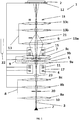
- Figure 1 schematically shows an electron beam system 1 suitable for acquiring multiple low magnification electron scattering angle distribution images 16 (not shown).
- the electron beam system 1 is a scanning transmission electron microscope (STEM) comprising a primary electron beam source 2 generating a primary electron beam 3 .
- the primary electron beam source may be a field emission, Schottky, thermionic emission type or others.
- the electron beam system further comprises a means for guiding the primary electron beam 3 and transmitted electron beam 6 containing a condenser lens system 8 , objective lens system 9 and projection lens system 13 .
- the shown condenser lens system 8 includes three lenses 8a , 8b and 8c for defining the size and convergence angle of the primary electron beam 3 .
- the objective lens system 9 is a Fourier type lens system where the object (not shown) situated in the object plane 5 lies above the center of the pole piece gap and the magnetic field of the objective lens 9 is strong enough to have the effect of three lenses.
- the lens 9a above the sample focuses the primary electron beam 3 and targets a point in the object plane 10 .
- the two objective lenses 9b and 9c downstream of the sample generates a first and second electron scattering angle distribution image 16 which is transferred by the projection lens system 13 to the detector 12.
- the projection lens system 13 is shown as three lenses 13a , 13b and 13c for creating a low magnification electron scattering angle distribution image 16 to illuminate a reduced subfield 19 (not shown) of the detector 12 .
- the electron beam system 1 further comprises a condenser aperture 20 and field limiting aperture 21 .
- the condenser aperture 20 is positioned upstream of the object plane 5 preferably below the first condenser 8a and depending on the position of the source image provided by condenser 8a defines the beam current.
- the condenser lenses 8b and 8c are then used to adjust the size and the convergence angle of the focused spot.
- the field limiting aperture 21 is positioned downstream of the object plane 10 and together with the projection lens system 13 can be used to restrict the electron scattering angle range and to give a sharp cut-off of the electron scattering angle distribution image 16 to limit the interaction from the adjacent subfields 19 (not shown).
- the electron beam system 1 further comprises a scan system 4 for scanning of the primary electron beam 3 over the object plane 5 , where the primary electron beam 3 interacts with the object in object plane 5 , and forms the transmitted electron beam 6 in the form of an electron scattering angle distribution image 16 . Downstream of the objective lens 9 the transmitted electron beam 6 is deflected by a descan system 7 back to the optical axis 10 of the electron beam system 1 .
- the scan system 4 may be further combined with a precession system 11 used to tilt the primary electron beam 3 by a small angle with respect to the optical axis 10 or shifted axis approximately parallel with the optical axis 10 , typically 0.3-3.0 degrees, and then rotate the tilted primary electron beam 3 around the optical axis 10 or shifted axis targeting a single point in the object plane 5 (respectively around the central ray if the primary electron beam 3 is scanned).
- the deprecession system 15 positioned downstream of the object plane 5 is used to compensate the effect of the precession system 11 , in order to achieve a stationary electron scattering angle distribution image 16 (diffraction pattern) at the detector plane 14 of the detector 12 .
- the scan system 4 along with the precession system 11 as well as the descan system 7 along with the deprecession system 15 may be situated in shared housing 17 .
- the transmitted electron beam 6 is deflected by a detector scan system 18 .
- the detector scan system 18 is dedicated for deflecting the transmitted electron beam 6 out of the optical axis 10 , creating a scattering angle distribution image 16 which may be positioned away from the optical axis 10 and the detector scan may be shifted stepwise over the detector 12 .
- the readout interval of the detector 12 is set up to be long enough for scanning at least two electron scattering angle distribution images 16 on the detector 12 during one readout interval. In the period of stepwise move and readout interval the beam is blanked with a beam blanker 23 .
- the beam blanker is able to shift the primary electron beam 3 or transmitted electron beam 6 so that no electron scattering angle distribution image 16 is reaching the detector 12 .
- the detector 12 is a multi-pixel detector (e.g. CMOS, CCD, image plate, multichannel plate) with a detector plane 14 facing the detector scan system 18 .
- the images captured on the detector 12 are stored in image storage device 24 .
- the electron scattering angle distribution image 16 may be formed and scanned over the detector plane 14 (not shown) according a beam scanning protocol controlled by the control unit 22 .
- This protocol may define: the setup of the condenser lens system 8 , objective lens system 9 and projection lens system 13 for achieving low magnification of the electron scattering angle distribution image 16 at the detector plane 12 ; the setup of the scan system 4 and/or the precession system 11 and the descan system 7 and/or the deprecession system 15 for selecting the scan mode (for example raster or line), scan speed, scan area and precession angle and precession speed; the setup of the detector scan system 18 for selecting the distance and direction between positions of the electron scattering angle distribution images 16 on the detector 12 ; and synchronization of the beam blanker 23 , the scan system 4 , descan system 7 , precession system 11 , deprecession system 15 and detector scan systems 18 with each other and with the detector 12 readout.
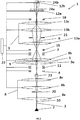
- Figure 2 schematically shows another example of an electron beam system 1 suitable for acquiring multiple low magnification electron scattering angle distribution images 16 .
- the objective lens system 9 is designed as common condenser objective lens type. In this type compares to the Fourier type lens, the sample is arranged in the center of the pole piece gap, and the field below the sample only has the effect of one objective lens and therefore only generates a single diffraction image (and a real image close to the first projector lens 13a ).
- the scan system 4 , descan system 7 , precession system 11 and deprecession system 15 are designed as independent systems.
- the electron beam system 1 is equipped with another detection system comprising at least two detectors 12a and 12b from which at least one is a two-dimensional detector 12 .
- Detectors 12a , 12b detect transmitted electrons which have scattered at different ranges of angles or are deflected by detector deflection system 18 at different range of angles.
- the images captured on the detectors 12a and 12b are stored in image storage devices 24a and 24b .
- FIG 3 schematically shows a preferred embodiment of a detector scan system 18 .
- the detector scan system 18 is positioned downstream of the projection lens system 13 .
- Application of a voltage to the detector scan systems 18 deflects the transmitted electron beam 6 by an angle a from the optical axis 10 and creates a scattering angle distribution image 16 on the detector plane 14 which may be positioned off of the optical axis.
- a stepwise change of the voltage on the detector scan system 18 will scan the scattering angle distribution image 16 stepwise over the detector plane 14 . Multiple images are then created by two or more electron scattering angle distribution images 16 .
- FIG. 4 schematically shows a top down view of the detector 12 .
- the detector plane 14 may be an imaging surface of a CMOS chip with a pixel resolution of 2560 x 2160 pixels.
- This detector plane 14 may be subdivided into subfields 19 of a size that may optimally correspond with the diameter of the scattering angle distribution image 16 so that the diameter of the scattering angle distribution image 16 fits into a subfield 19 .
- the diameter of the scattering angle distribution image 16 is 256 pixels, up to 80 scattering angle distribution images 16 may be placed side by side on a detector 14 with 2560 x 2160 pixels before readout takes place.
- the diameter of the scattering angle distribution image 16 may be adjusted to another size so that more than one scattering angle distribution image 16 may be recorded on the detector 14 before readout takes place.
- FIG. 5 Shows an example of the sub-field scan strategy.
- Fig. 5a is a raster scan strategy where the detector scan system 18 deflects the scattering angle distribution image 16 stepwise over the subfields 19 in straight parallel lines with all lines in the same direction.
- FIG. 5b shows the meander scan strategy where the scattering angle distribution image 16 is not moved to the beginning of the next line but is moved to the line just below the current line and continues to move in the opposite direction to the current line.
- FIG. 5c shows the spiral scan strategy where the scattering angle distribution image 16 is moved in a spiral manner. These strategies are applied until more than two subfields 19 are exposed.
Landscapes
- Chemical & Material Sciences (AREA)
- Analytical Chemistry (AREA)
- Crystallography & Structural Chemistry (AREA)
- Physics & Mathematics (AREA)
- Health & Medical Sciences (AREA)
- Life Sciences & Earth Sciences (AREA)
- Biochemistry (AREA)
- General Health & Medical Sciences (AREA)
- General Physics & Mathematics (AREA)
- Immunology (AREA)
- Pathology (AREA)
- Analysing Materials By The Use Of Radiation (AREA)
Priority Applications (2)
| Application Number | Priority Date | Filing Date | Title |
|---|---|---|---|
| EP17000450.1A EP3379557A1 (fr) | 2017-03-20 | 2017-03-20 | Microscope électronique à transmission et à balayage et procédé d'acquisition à haut rendement des images de la distribution de l'angle de diffusion d'électrons |
| EP18162997.3A EP3392900B1 (fr) | 2017-03-20 | 2018-03-20 | Procédé d'alignement automatique d'un microscope électronique par transmission à balayage pour le mappage de données de diffraction d'électrons par précession |
Applications Claiming Priority (1)
| Application Number | Priority Date | Filing Date | Title |
|---|---|---|---|
| EP17000450.1A EP3379557A1 (fr) | 2017-03-20 | 2017-03-20 | Microscope électronique à transmission et à balayage et procédé d'acquisition à haut rendement des images de la distribution de l'angle de diffusion d'électrons |
Publications (1)
| Publication Number | Publication Date |
|---|---|
| EP3379557A1 true EP3379557A1 (fr) | 2018-09-26 |
Family
ID=58401323
Family Applications (1)
| Application Number | Title | Priority Date | Filing Date |
|---|---|---|---|
| EP17000450.1A Withdrawn EP3379557A1 (fr) | 2017-03-20 | 2017-03-20 | Microscope électronique à transmission et à balayage et procédé d'acquisition à haut rendement des images de la distribution de l'angle de diffusion d'électrons |
Country Status (1)
| Country | Link |
|---|---|
| EP (1) | EP3379557A1 (fr) |
Cited By (4)
| Publication number | Priority date | Publication date | Assignee | Title |
|---|---|---|---|---|
| CN109166781A (zh) * | 2018-09-11 | 2019-01-08 | 镇江乐华电子科技有限公司 | 扫描透射电子显微成像方法和系统 |
| JP2024540800A (ja) * | 2021-09-01 | 2024-11-06 | フィジカルニ ウースタヴ アーヴェー チェーエル ヴェーヴェーイー | 結晶構造を決定する方法及びそれを実施するための装置 |
| EP4528257A1 (fr) * | 2023-09-22 | 2025-03-26 | Fei Company | Imagerie par moiré améliorée par un dispositif de suppression |
| US12417893B2 (en) | 2019-05-20 | 2025-09-16 | Eldico Scientific Ag | Diffractometer for charged-particle crystallography |
Citations (3)
| Publication number | Priority date | Publication date | Assignee | Title |
|---|---|---|---|---|
| US4514629A (en) * | 1982-07-07 | 1985-04-30 | National Research Development Corporation | Scanning transmission electron microscopes |
| US20070023659A1 (en) * | 2003-09-02 | 2007-02-01 | Sergeevich Avilov A | Method for measuring diffraction patterns from a transmission electron microscopy to determine crystal structures and a device therefor |
| US8253099B2 (en) | 2008-11-06 | 2012-08-28 | Nanomegas Sprl | Methods and devices for high throughput crystal structure analysis by electron diffraction |
-
2017
- 2017-03-20 EP EP17000450.1A patent/EP3379557A1/fr not_active Withdrawn
Patent Citations (3)
| Publication number | Priority date | Publication date | Assignee | Title |
|---|---|---|---|---|
| US4514629A (en) * | 1982-07-07 | 1985-04-30 | National Research Development Corporation | Scanning transmission electron microscopes |
| US20070023659A1 (en) * | 2003-09-02 | 2007-02-01 | Sergeevich Avilov A | Method for measuring diffraction patterns from a transmission electron microscopy to determine crystal structures and a device therefor |
| US8253099B2 (en) | 2008-11-06 | 2012-08-28 | Nanomegas Sprl | Methods and devices for high throughput crystal structure analysis by electron diffraction |
Cited By (4)
| Publication number | Priority date | Publication date | Assignee | Title |
|---|---|---|---|---|
| CN109166781A (zh) * | 2018-09-11 | 2019-01-08 | 镇江乐华电子科技有限公司 | 扫描透射电子显微成像方法和系统 |
| US12417893B2 (en) | 2019-05-20 | 2025-09-16 | Eldico Scientific Ag | Diffractometer for charged-particle crystallography |
| JP2024540800A (ja) * | 2021-09-01 | 2024-11-06 | フィジカルニ ウースタヴ アーヴェー チェーエル ヴェーヴェーイー | 結晶構造を決定する方法及びそれを実施するための装置 |
| EP4528257A1 (fr) * | 2023-09-22 | 2025-03-26 | Fei Company | Imagerie par moiré améliorée par un dispositif de suppression |
Similar Documents
| Publication | Publication Date | Title |
|---|---|---|
| US9449789B2 (en) | Apparatus and method for inspecting a surface of a sample | |
| JP4597207B2 (ja) | 走査電子顕微鏡 | |
| JP7105647B2 (ja) | 透過型荷電粒子顕微鏡における回折パターン検出 | |
| EP1453077A2 (fr) | Microscope électronique à balayage et méthode d'observation d'un échantillon | |
| EP3258477B1 (fr) | Microscope électronique et procédé d'acquisition d'image | |
| JP4800211B2 (ja) | 走査型電子顕微鏡用の検出器システムおよび対応する検出器システムを備える走査型電子顕微鏡 | |
| EP4067886A1 (fr) | Procédé et système pour déterminer la structure cristalline | |
| JP6876418B2 (ja) | 画像取得方法および電子顕微鏡 | |
| US10699872B2 (en) | Discriminative imaging technique in scanning transmission charged particle microscopy | |
| JP2005235665A (ja) | 暗視野走査透過電子顕微鏡および観察方法 | |
| US20220181117A1 (en) | Method and system for generating reciprocal space map | |
| JP2006153894A (ja) | 電子線を用いた観察装置及び観察方法 | |
| JP7852821B2 (ja) | 三次元電子回折データを取得するための方法およびシステム | |
| JP3571561B2 (ja) | 走査顕微鏡 | |
| Holm et al. | STEM in SEM: Introduction to Scanning Transmission Electron Microscopy for Microelectronics Failure Analysis | |
| JP2006331901A (ja) | 位相回復方式の電子顕微鏡による観察方法 | |
| EP4632787A1 (fr) | Procédé d'obtention d'une série d'images à inclinaison d'un échantillon à une pluralité d'angles d'inclinaison | |
| JPH1167138A (ja) | 微小領域観察装置 | |
| JP2003317654A (ja) | 電子顕微方法及びそれを用いた電子顕微鏡並び生体試料検査方法及び生体検査装置 | |
| JP2025080553A (ja) | 観察方法および観察装置 | |
| Holm et al. | Imaging and Diffraction with a Programmable Pixelated Detector | |
| JP2006302523A (ja) | 走査像観察機能を有した透過電子顕微鏡 | |
| JP2007287561A (ja) | 荷電粒子線装置 | |
| JPH06123720A (ja) | 表面観察装置 | |
| JPH02204954A (ja) | 走査型透過電子顕微鏡法 |
Legal Events
| Date | Code | Title | Description |
|---|---|---|---|
| PUAI | Public reference made under article 153(3) epc to a published international application that has entered the european phase |
Free format text: ORIGINAL CODE: 0009012 |
|
| STAA | Information on the status of an ep patent application or granted ep patent |
Free format text: STATUS: REQUEST FOR EXAMINATION WAS MADE |
|
| 17P | Request for examination filed |
Effective date: 20180222 |
|
| AK | Designated contracting states |
Kind code of ref document: A1 Designated state(s): AL AT BE BG CH CY CZ DE DK EE ES FI FR GB GR HR HU IE IS IT LI LT LU LV MC MK MT NL NO PL PT RO RS SE SI SK SM TR |
|
| AX | Request for extension of the european patent |
Extension state: BA ME |
|
| RBV | Designated contracting states (corrected) |
Designated state(s): AL AT BE BG CH CY CZ DE DK EE ES FI FR GB GR HR HU IE IS IT LI LT LU LV MC MK MT NL NO PL PT RO RS SE SI SK SM TR |
|
| STAA | Information on the status of an ep patent application or granted ep patent |
Free format text: STATUS: THE APPLICATION IS DEEMED TO BE WITHDRAWN |
|
| 18D | Application deemed to be withdrawn |
Effective date: 20201001 |