EP3379580A1 - Dispositif à semi-conducteur en diamant - Google Patents
Dispositif à semi-conducteur en diamant Download PDFInfo
- Publication number
- EP3379580A1 EP3379580A1 EP17162272.3A EP17162272A EP3379580A1 EP 3379580 A1 EP3379580 A1 EP 3379580A1 EP 17162272 A EP17162272 A EP 17162272A EP 3379580 A1 EP3379580 A1 EP 3379580A1
- Authority
- EP
- European Patent Office
- Prior art keywords
- substrate
- electrically conductive
- conductive portion
- diamond
- semiconducting
- Prior art date
- Legal status (The legal status is an assumption and is not a legal conclusion. Google has not performed a legal analysis and makes no representation as to the accuracy of the status listed.)
- Withdrawn
Links
Images




Classifications
-
- H—ELECTRICITY
- H10—SEMICONDUCTOR DEVICES; ELECTRIC SOLID-STATE DEVICES NOT OTHERWISE PROVIDED FOR
- H10D—INORGANIC ELECTRIC SEMICONDUCTOR DEVICES
- H10D8/00—Diodes
-
- H—ELECTRICITY
- H01—ELECTRIC ELEMENTS
- H01J—ELECTRIC DISCHARGE TUBES OR DISCHARGE LAMPS
- H01J1/00—Details of electrodes, of magnetic control means, of screens, or of the mounting or spacing thereof, common to two or more basic types of discharge tubes or lamps
- H01J1/02—Main electrodes
- H01J1/30—Cold cathodes, e.g. field-emissive cathode
- H01J1/304—Field-emissive cathodes
- H01J1/3042—Field-emissive cathodes microengineered, e.g. Spindt-type
- H01J1/3044—Point emitters
-
- H—ELECTRICITY
- H01—ELECTRIC ELEMENTS
- H01J—ELECTRIC DISCHARGE TUBES OR DISCHARGE LAMPS
- H01J1/00—Details of electrodes, of magnetic control means, of screens, or of the mounting or spacing thereof, common to two or more basic types of discharge tubes or lamps
- H01J1/02—Main electrodes
- H01J1/30—Cold cathodes, e.g. field-emissive cathode
- H01J1/308—Semiconductor cathodes, e.g. cathodes with PN junction layers
-
- H—ELECTRICITY
- H01—ELECTRIC ELEMENTS
- H01J—ELECTRIC DISCHARGE TUBES OR DISCHARGE LAMPS
- H01J9/00—Apparatus or processes specially adapted for the manufacture, installation, removal, maintenance of electric discharge tubes, discharge lamps, or parts thereof; Recovery of material from discharge tubes or lamps
- H01J9/02—Manufacture of electrodes or electrode systems
- H01J9/022—Manufacture of electrodes or electrode systems of cold cathodes
- H01J9/025—Manufacture of electrodes or electrode systems of cold cathodes of field emission cathodes
-
- H—ELECTRICITY
- H10—SEMICONDUCTOR DEVICES; ELECTRIC SOLID-STATE DEVICES NOT OTHERWISE PROVIDED FOR
- H10D—INORGANIC ELECTRIC SEMICONDUCTOR DEVICES
- H10D62/00—Semiconductor bodies, or regions thereof, of devices having potential barriers
- H10D62/10—Shapes, relative sizes or dispositions of the regions of the semiconductor bodies; Shapes of the semiconductor bodies
- H10D62/102—Constructional design considerations for preventing surface leakage or controlling electric field concentration
-
- H—ELECTRICITY
- H10—SEMICONDUCTOR DEVICES; ELECTRIC SOLID-STATE DEVICES NOT OTHERWISE PROVIDED FOR
- H10D—INORGANIC ELECTRIC SEMICONDUCTOR DEVICES
- H10D62/00—Semiconductor bodies, or regions thereof, of devices having potential barriers
- H10D62/80—Semiconductor bodies, or regions thereof, of devices having potential barriers characterised by the materials
- H10D62/83—Semiconductor bodies, or regions thereof, of devices having potential barriers characterised by the materials being Group IV materials, e.g. B-doped Si or undoped Ge
- H10D62/8303—Diamond
-
- H—ELECTRICITY
- H10—SEMICONDUCTOR DEVICES; ELECTRIC SOLID-STATE DEVICES NOT OTHERWISE PROVIDED FOR
- H10D—INORGANIC ELECTRIC SEMICONDUCTOR DEVICES
- H10D8/00—Diodes
- H10D8/01—Manufacture or treatment
-
- H—ELECTRICITY
- H10—SEMICONDUCTOR DEVICES; ELECTRIC SOLID-STATE DEVICES NOT OTHERWISE PROVIDED FOR
- H10P—GENERIC PROCESSES OR APPARATUS FOR THE MANUFACTURE OR TREATMENT OF DEVICES COVERED BY CLASS H10
- H10P50/00—Etching of wafers, substrates or parts of devices
-
- H—ELECTRICITY
- H01—ELECTRIC ELEMENTS
- H01J—ELECTRIC DISCHARGE TUBES OR DISCHARGE LAMPS
- H01J2201/00—Electrodes common to discharge tubes
- H01J2201/30—Cold cathodes
- H01J2201/304—Field emission cathodes
- H01J2201/30403—Field emission cathodes characterised by the emitter shape
- H01J2201/30407—Microengineered point emitters
- H01J2201/30411—Microengineered point emitters conical shaped, e.g. Spindt type
-
- H—ELECTRICITY
- H01—ELECTRIC ELEMENTS
- H01J—ELECTRIC DISCHARGE TUBES OR DISCHARGE LAMPS
- H01J2201/00—Electrodes common to discharge tubes
- H01J2201/30—Cold cathodes
- H01J2201/304—Field emission cathodes
- H01J2201/30446—Field emission cathodes characterised by the emitter material
- H01J2201/30453—Carbon types
- H01J2201/30457—Diamond
-
- H—ELECTRICITY
- H01—ELECTRIC ELEMENTS
- H01J—ELECTRIC DISCHARGE TUBES OR DISCHARGE LAMPS
- H01J2201/00—Electrodes common to discharge tubes
- H01J2201/30—Cold cathodes
- H01J2201/304—Field emission cathodes
- H01J2201/30446—Field emission cathodes characterised by the emitter material
- H01J2201/3048—Semiconductor materials
Definitions
- the present invention relates to an electrical device, and relates particularly to an electrical device adapted to generate free electrons by means of solid-state field emission.
- Silicon has limitations when used as a base electronic material for switching and amplification applications in high power, high frequency and extreme environments. It is known that diamond is a more suitable material than silicon in such environments because of its thermal, dielectric and carrier mobility properties, and devices made from diamond offer the possibility of significantly reducing complexity by reducing the number of discrete devices needed to carry out an application.
- boron doped diamond is a reasonably effective p type semiconductor
- no effective n type dopant has yet been found, since both dopant species are deep donors with activation energies of 0.7 eV and 4.5 eV respectively, leading to the requirement for heating to assist the release of charge carriers in order to realise effective device operation.
- the process of heating also causes a reduction in carrier mobility and electric field breakdown strength, thereby compromising two of the main features that make diamond suitable for the fabrication of high power switches.
- the arrangement described by Geis et al uses substitutional nitrogen as an n type dopant in the diamond layer, which enhances the electric field in the vicinity of the tip of the electron emitter.
- this arrangement suffers from the drawback that the n type dopant in the diamond substrate further away from the metal-diamond interface at the tip of the electron emitter inhibits conduction of electrons through the diamond substrate.
- EP 2605282 A further known device is disclosed in EP 2605282 , which uses a unipolar structure which enables the material properties of diamond to be exploited, and in effect replaces the vacuum described above with diamond.
- this arrangement suffers from the drawback that its performance is limited by the low n type dopant densities that can be achieved with nitrogen in diamond and the associated high activation energy.
- Preferred embodiments of the present invention seek to overcome one or more of the above disadvantages of the prior art.
- an electrical device comprising:
- this provides the advantage of enhancing the local electric field at the interface with the conductive portion, by creating a highly defined region of positive space charge around the conductive portion that greatly improves the efficiency by which electrons are transferred from the conductive medium into the diamond substrate, thereby enabling larger current conduction.
- the invention has the further advantage that by making the semiconducting region sufficiently thin, the lattice stress caused by introduction of the dopant is relatively insignificant, and a wider choice of dopant materials is available.
- the advantage is provided that the diamond substrate can remain undoped, as a result of which the inhibiting effect of doped diamond on electron conduction can be minimised.
- At least one said semiconducting region may include diamond.
- At least one said semiconducting region may include at least one donor dopant to impart an n-type semiconducting characteristic to said region.
- At least one said semiconducting region may include a plurality of dopant materials so as to impart an n-type semiconducting characteristic to said region.
- At least one said dopant may be a group I element.
- At least one said dopant may be a group V element.
- At least one said dopant may be a group VI element.
- At least one said first electrically conductive portion may be adapted to locally enhance said electric field.
- At least one said first electrically conductive portion may include at least one metal that forms a Schottky junction with the semiconducting region.
- the device may further comprise at least one second electrically conductive portion connected to at least one said first electrically conductive portion.
- This provides the advantage of enabling suitable conductive tracking of the material to be selected.
- the device may further comprise at least one first terminating material terminating at least part of a surface of at least one said semiconducting region to impart positive electron affinity thereto.
- At least one said first terminating material may comprise oxygen.
- At least one said first terminating material may comprise fluorine.
- At least one said semiconducting region may include diamond.
- At least one said semiconducting region may include at least one donor dopant to impart an n-type semiconducting characteristic to said region.
- At least one said semiconducting region may include a plurality of dopant materials to impart an n-type semiconducting characteristic to said region.
- At least one said dopant may be a group I element.
- At least one said dopant may be a group V element.
- At least one said dopant may be a group VI element.
- At least one said first electrically conductive portion may be adapted to locally enhance said electric field.
- the method may further comprise applying at least one second electrically conductive portion to at least one said first electrically conductive portion.
- the method may further comprise terminating at least part of a surface of at least one said semiconducting region to impart positive electron affinity thereto.
- the step of forming at least one recess in a substrate of diamond material may comprise arranging at least one catalytic material on a surface of said substrate, causing said catalytic material to convert diamond in contact therewith into non-diamond carbon material, and causing said catalytic material to penetrate said substrate.
- a diode type electrical switching device 2 has a diamond substrate 4, in a surface of which recesses 6 are formed by means of an etching process that yields a point with low radius of curvature, for example as defined in EP 2605282 .
- the recesses 6 are preferably elongate in shape, and preferably have side walls 8 generally perpendicular to an upper surface 10 of the substrate 4 and to further decrease the radius of curvature feature inclined distal surfaces 12. This shape of recesses 6 contributes significantly to electric field enhancement in the completed device 2, as will be described in further detail below.
- the semiconductor layer 14 can be made sufficiently thin that the addition of the dopant to the semiconductor layer 14 does not cause significant lattice stress in the diamond semiconductor layer 14.
- a surface 16 of the semiconductor layer 14 facing away from the substrate 4 is modified to impart positive electron affinity to the semiconductor layer 14.
- a very heavily oxidising solution such as a mixture of concentrated sulphuric acid and hydrogen peroxide at more than 100°C for at least 30 minutes
- treatment in a plasma chamber containing an inert gas and oxygen or heating the diamond layer 14 in a low pressure oxygen atmosphere to 400°C for 30 minutes, or any combination of the above steps.
- the surface can be terminated using fluorine.
- the recesses 6 are filled with a first electrically conductive material in the form of elongate metal protrusions 18.
- the protrusions 18 are formed from a metal which exhibits the Schottky effect when in contact with diamond, for example gold, platinum, ruthenium or silver, but generally includes any metal that does not naturally form a carbide with diamond when annealed.
- the surface termination 16 of the diamond semiconductor layer 14 causes the barrier height between the conductive metal protrusions 18 and the semiconductor diamond layer 14 to be reduced, thereby improving the efficiency with which electrons can tunnel into the conduction band of the bulk diamond substrate 4.
- a second electrically conductive material in the form of a further metal layer 20 is applied to the conductive metal protrusions 18 to provide additional electrical current carrying capacity and to facilitate easier bonding of the contacts in a device package.
- An electrode 22 of suitable metal is applied to the opposite surface of the substrate 4 to the metal protrusions 18.
- the electric field in the metal protrusions 18 is strongest at the distal ends of the protrusions 18.
- the n type diamond semiconductor layer 14 loses spare electrons from the dopant material in the layer 14, thereby becoming depleted and creating a region of positive space charge around the distal ends of the metal protrusions 18, as illustrated in Figure 3 . This significantly enhances the local electric field, such that conditions for Fowler-Nordheim quantum mechanical tunnelling can be met.
- the semiconductor layer 14 is fully thermally and electrically compatible with the diamond substrate 4, although it will be appreciated by persons skilled in the art that materials other than diamond can be used to create a depletion effect. Electrons are emitted from the distal ends of the metal protrusions 18, and the enhanced electric field created by the semiconductor layer 14 provides sufficient potential to accelerate electrons through the positively charged semiconductor layer 14 into the diamond substrate 4.
- the semiconductor layer can be made of sufficiently small thickness (typically in the region of 20 nm) that the layer 14 does not develop lattice stress, thereby enabling use of elements such as nitrogen and phosphorous as dopants.
- the semiconductor layer 14 loses excess electrons into the bulk diamond substrate 4, and this process is enhanced by the high electric field generated by the elongate structure of the metal protrusions 18. Because the electrons are close to the conduction band of diamond, this process requires lower voltages than would be required to cause an electron to move directly from a metal protrusion 18 into the diamond substrate 4.
- the semiconductor layer 14 becomes depleted of electrons and becomes highly positively space charged, which causes the electric field across the semiconductor layer 14 to exceed the approximately 10 7 Vmm -1 field condition necessary to stimulate Fowler-Nordheim tunnelling from the junction of the metal protrusions 18 and the semiconductor layer 14.
- the metal protrusions 18 are caused to inject electrons to neutralise the positive space charge, but because the semiconductor layer 14 is so thin, electrons pass directly through the semiconductor layer 14 into the diamond substrate 4 without significantly neutralising the space charge.
- the thickness of the semiconductor layer 14 By suitable choice of the thickness of the semiconductor layer 14, it can be ensured that the local electric field is sufficiently concentrated that the 10 7 Vmm -1 criterion for tunnelling emission is met, but that the field also rapidly diminishes so that emitted electrons are not accelerated to the extent that electrons then collide inelastically with carbon atoms in the lattice of the bulk diamond 4, which could cause the atoms to become ionised, which in turn could cause an avalanche process that could destroy the device 2.
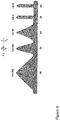
- Figure 4 shows the effect of the shape of the conductive metal protrusions 18 on electric field enhancement.
- the level of field intensification relative to an expected uniform field referred to as the ⁇ factor, is related to the ratio of the protrusion height above the plane at its base, and its diameter, although the geometric shape also has an effect.
- the shape of the protrusions 18 shown in Figure 1 has a significantly enhanced effect on the electric field.
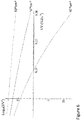
- Figure 5 shows the effect of dopant concentration in the semiconductor layer 14 on electric field enhancement.
- the level of dopant concentration has an effect both on the amplification of the electric field around a metal protrusion 18, and the current emitted from each protrusion 18.
- the dopant level in the semiconductor layer 14 also has an effect on the current density of electron emission from the tip of each protrusion 18. This is shown in Figure 6 .
- the thickness of the semiconductor layer 14 also has an effect on the effectiveness of the device 2.
- the high electric fields generated within the depletion layer formed at the point of emission at the tips of the protrusions 18 exceeds the insulation strength of the base diamond material.
- the layer thickness needs to be restricted so that the energy imparted to the electrons during transit is insufficient to accelerate them to the velocities which would cause this effect. This is expressed in terms of the Debye length, which is itself determined by the dopant concentration in the semiconductor layer 14, as shown in Figure 5 .
- the dopant concentration level should be in excess of 10 18 atoms per cm 3 , and preferably in excess of 10 20 atoms per cm 3 to maximise field enhancement. This suggests a thickness of the semiconductor layer 14 in the region of 1-10 Debye lengths.
- the diamond substrate 4 used in the present invention can be made from single crystal diamond, but the principles of the invention described above could also be applied to nano-crystalline diamond. In the latter case, the shape of the hole is more likely to be an elongate cylinder.
Landscapes
- Engineering & Computer Science (AREA)
- Manufacturing & Machinery (AREA)
- Cold Cathode And The Manufacture (AREA)
- Electrodes Of Semiconductors (AREA)
- Crystals, And After-Treatments Of Crystals (AREA)
- Electrical Discharge Machining, Electrochemical Machining, And Combined Machining (AREA)
- Control Of Electric Motors In General (AREA)
Priority Applications (8)
| Application Number | Priority Date | Filing Date | Title |
|---|---|---|---|
| EP17162272.3A EP3379580A1 (fr) | 2017-03-22 | 2017-03-22 | Dispositif à semi-conducteur en diamant |
| CN201880019196.5A CN110431670A (zh) | 2017-03-22 | 2018-02-28 | 金刚石半导体器件 |
| KR1020197027225A KR102414061B1 (ko) | 2017-03-22 | 2018-02-28 | 다이아몬드 반도체 장치 |
| PCT/EP2018/054929 WO2018172029A1 (fr) | 2017-03-22 | 2018-02-28 | Dispositif à semiconducteur au diamant |
| US16/495,784 US11011605B2 (en) | 2017-03-22 | 2018-02-28 | Diamond semiconductor device |
| JP2019551710A JP7069203B2 (ja) | 2017-03-22 | 2018-02-28 | ダイヤモンド半導体装置 |
| EP18709312.5A EP3602634A1 (fr) | 2017-03-22 | 2018-02-28 | Dispositif à semiconducteur au diamant |
| TW107109099A TWI782961B (zh) | 2017-03-22 | 2018-03-16 | 電氣裝置及形成電氣裝置的方法 |
Applications Claiming Priority (1)
| Application Number | Priority Date | Filing Date | Title |
|---|---|---|---|
| EP17162272.3A EP3379580A1 (fr) | 2017-03-22 | 2017-03-22 | Dispositif à semi-conducteur en diamant |
Publications (1)
| Publication Number | Publication Date |
|---|---|
| EP3379580A1 true EP3379580A1 (fr) | 2018-09-26 |
Family
ID=58410130
Family Applications (2)
| Application Number | Title | Priority Date | Filing Date |
|---|---|---|---|
| EP17162272.3A Withdrawn EP3379580A1 (fr) | 2017-03-22 | 2017-03-22 | Dispositif à semi-conducteur en diamant |
| EP18709312.5A Withdrawn EP3602634A1 (fr) | 2017-03-22 | 2018-02-28 | Dispositif à semiconducteur au diamant |
Family Applications After (1)
| Application Number | Title | Priority Date | Filing Date |
|---|---|---|---|
| EP18709312.5A Withdrawn EP3602634A1 (fr) | 2017-03-22 | 2018-02-28 | Dispositif à semiconducteur au diamant |
Country Status (7)
| Country | Link |
|---|---|
| US (1) | US11011605B2 (fr) |
| EP (2) | EP3379580A1 (fr) |
| JP (1) | JP7069203B2 (fr) |
| KR (1) | KR102414061B1 (fr) |
| CN (1) | CN110431670A (fr) |
| TW (1) | TWI782961B (fr) |
| WO (1) | WO2018172029A1 (fr) |
Families Citing this family (3)
| Publication number | Priority date | Publication date | Assignee | Title |
|---|---|---|---|---|
| WO2020230520A1 (fr) * | 2019-05-10 | 2020-11-19 | 国立研究開発法人産業技術総合研究所 | Corps composite comprenant un corps de cristal de diamant |
| CN112133752B (zh) * | 2020-08-27 | 2021-11-19 | 西安电子科技大学 | 一种复合终端表面金刚石高压场效应晶体管及其制作方法 |
| EP3989260A1 (fr) | 2020-10-22 | 2022-04-27 | Evince Technology Ltd | Appareil de production de matières gazeuses ou de vapeur ionisées |
Citations (3)
| Publication number | Priority date | Publication date | Assignee | Title |
|---|---|---|---|---|
| JP2000106435A (ja) * | 1998-09-29 | 2000-04-11 | Toshiba Corp | 電力用素子 |
| EP2605282A2 (fr) | 2006-06-13 | 2013-06-19 | Evince Technology Limited | Dispositif de commutation électrique en diamant. |
| US20140145210A1 (en) * | 2012-11-28 | 2014-05-29 | Kabushiki Kaisha Toshiba | Semiconductor device |
Family Cites Families (11)
| Publication number | Priority date | Publication date | Assignee | Title |
|---|---|---|---|---|
| US5713775A (en) * | 1995-05-02 | 1998-02-03 | Massachusetts Institute Of Technology | Field emitters of wide-bandgap materials and methods for their fabrication |
| US6554673B2 (en) * | 2001-07-31 | 2003-04-29 | The United States Of America As Represented By The Secretary Of The Navy | Method of making electron emitters |
| JP4539011B2 (ja) * | 2002-02-20 | 2010-09-08 | 富士電機システムズ株式会社 | 半導体装置 |
| WO2003106743A1 (fr) * | 2002-06-01 | 2003-12-24 | 住友電気工業株式会社 | Procede de production de diamant semi-conducteur de type n et diamant semi-conducteur |
| EP2790207B1 (fr) * | 2005-06-20 | 2016-01-06 | Nippon Telegraph And Telephone Corporation | Élément semi-conducteur en diamant et son procédé de fabrication |
| US8637386B2 (en) * | 2009-05-12 | 2014-01-28 | Cree, Inc. | Diffused junction termination structures for silicon carbide devices and methods of fabricating silicon carbide devices incorporating same |
| US8264047B2 (en) * | 2010-05-10 | 2012-09-11 | Infineon Technologies Austria Ag | Semiconductor component with a trench edge termination |
| US9318623B2 (en) * | 2011-04-05 | 2016-04-19 | Cree, Inc. | Recessed termination structures and methods of fabricating electronic devices including recessed termination structures |
| US9219020B2 (en) * | 2012-03-08 | 2015-12-22 | Infineon Technologies Ag | Semiconductor device, wafer assembly and methods of manufacturing wafer assemblies and semiconductor devices |
| JP6203074B2 (ja) * | 2014-02-17 | 2017-09-27 | 株式会社東芝 | 半導体装置およびその製造方法 |
| US10700165B2 (en) * | 2016-06-17 | 2020-06-30 | Adamantite Technologies LLC | Doped diamond SemiConductor and method of manufacture using laser abalation |
-
2017
- 2017-03-22 EP EP17162272.3A patent/EP3379580A1/fr not_active Withdrawn
-
2018
- 2018-02-28 JP JP2019551710A patent/JP7069203B2/ja not_active Expired - Fee Related
- 2018-02-28 US US16/495,784 patent/US11011605B2/en not_active Expired - Fee Related
- 2018-02-28 CN CN201880019196.5A patent/CN110431670A/zh active Pending
- 2018-02-28 EP EP18709312.5A patent/EP3602634A1/fr not_active Withdrawn
- 2018-02-28 KR KR1020197027225A patent/KR102414061B1/ko not_active Expired - Fee Related
- 2018-02-28 WO PCT/EP2018/054929 patent/WO2018172029A1/fr not_active Ceased
- 2018-03-16 TW TW107109099A patent/TWI782961B/zh not_active IP Right Cessation
Patent Citations (3)
| Publication number | Priority date | Publication date | Assignee | Title |
|---|---|---|---|---|
| JP2000106435A (ja) * | 1998-09-29 | 2000-04-11 | Toshiba Corp | 電力用素子 |
| EP2605282A2 (fr) | 2006-06-13 | 2013-06-19 | Evince Technology Limited | Dispositif de commutation électrique en diamant. |
| US20140145210A1 (en) * | 2012-11-28 | 2014-05-29 | Kabushiki Kaisha Toshiba | Semiconductor device |
Non-Patent Citations (2)
| Title |
|---|
| M. W. GEIS ET AL.: "Diamond emitters fabrication and theory", J. VAC. SCI. TECHNOL., B, vol. 14, no. 3, May 1996 (1996-05-01), XP000621834, DOI: doi:10.1116/1.588986 |
| RIETWYK K J ET AL: "Work function and electron affinity of the fluorine-terminated (100) diamond surface", APPLIED PHYSICS LETTERS, A I P PUBLISHING LLC, US, vol. 102, no. 9, 4 March 2013 (2013-03-04), pages 91604 - 91604, XP012170290, ISSN: 0003-6951, [retrieved on 20130308], DOI: 10.1063/1.4793999 * |
Also Published As
| Publication number | Publication date |
|---|---|
| US20200027683A1 (en) | 2020-01-23 |
| CN110431670A (zh) | 2019-11-08 |
| EP3602634A1 (fr) | 2020-02-05 |
| JP7069203B2 (ja) | 2022-05-17 |
| WO2018172029A1 (fr) | 2018-09-27 |
| JP2020511798A (ja) | 2020-04-16 |
| KR102414061B1 (ko) | 2022-06-28 |
| TWI782961B (zh) | 2022-11-11 |
| TW201907571A (zh) | 2019-02-16 |
| KR20190129047A (ko) | 2019-11-19 |
| US11011605B2 (en) | 2021-05-18 |
Similar Documents
| Publication | Publication Date | Title |
|---|---|---|
| JP4857769B2 (ja) | 電子放出素子 | |
| WO1997039469A1 (fr) | Emetteurs d'electrons de grande energie | |
| US11011605B2 (en) | Diamond semiconductor device | |
| US20180374669A1 (en) | Electron transparent membrane for cold cathode devices | |
| JP5315236B2 (ja) | 電気スイッチングデバイス、及びダイヤモンド基板に触媒材料を埋め込む方法 | |
| US6008502A (en) | Diamond electron emitting device having an insulative electron supply layer | |
| US11177104B2 (en) | Device for controlling electron flow and method for manufacturing said device | |
| CN108615768B (zh) | 一种抗辐射vdmos器件及其制备方法 | |
| US11456175B2 (en) | Method of making a silicon carbide electronic device | |
| Li et al. | Study of ballasting carbon nanotube field emitter arrays with coaxial gate using doped silicon resistor | |
| TW202232545A (zh) | 用於產生電離氣體或蒸氣材料的設備 | |
| Parameswaran et al. | Field-Emitter-Array Cold Cathode Arc-Protection Methods-A Theoretical Study | |
| WO2016024878A1 (fr) | Dispositif permettant l'extraction d'électrons dans des systèmes d'émission par effet de champ, et procédé de formation du dispositif |
Legal Events
| Date | Code | Title | Description |
|---|---|---|---|
| PUAI | Public reference made under article 153(3) epc to a published international application that has entered the european phase |
Free format text: ORIGINAL CODE: 0009012 |
|
| AK | Designated contracting states |
Kind code of ref document: A1 Designated state(s): AL AT BE BG CH CY CZ DE DK EE ES FI FR GB GR HR HU IE IS IT LI LT LU LV MC MK MT NL NO PL PT RO RS SE SI SK SM TR |
|
| AX | Request for extension of the european patent |
Extension state: BA ME |
|
| STAA | Information on the status of an ep patent application or granted ep patent |
Free format text: STATUS: THE APPLICATION IS DEEMED TO BE WITHDRAWN |
|
| 18D | Application deemed to be withdrawn |
Effective date: 20190327 |