EP3379662A1 - Amplificateur optique - Google Patents
Amplificateur optique Download PDFInfo
- Publication number
- EP3379662A1 EP3379662A1 EP15908762.6A EP15908762A EP3379662A1 EP 3379662 A1 EP3379662 A1 EP 3379662A1 EP 15908762 A EP15908762 A EP 15908762A EP 3379662 A1 EP3379662 A1 EP 3379662A1
- Authority
- EP
- European Patent Office
- Prior art keywords
- gain
- unit
- signal beam
- optical amplifier
- wavelength
- Prior art date
- Legal status (The legal status is an assumption and is not a legal conclusion. Google has not performed a legal analysis and makes no representation as to the accuracy of the status listed.)
- Granted
Links
Images




Classifications
-
- H—ELECTRICITY
- H01—ELECTRIC ELEMENTS
- H01S—DEVICES USING THE PROCESS OF LIGHT AMPLIFICATION BY STIMULATED EMISSION OF RADIATION [LASER] TO AMPLIFY OR GENERATE LIGHT; DEVICES USING STIMULATED EMISSION OF ELECTROMAGNETIC RADIATION IN WAVE RANGES OTHER THAN OPTICAL
- H01S3/00—Lasers, i.e. devices using stimulated emission of electromagnetic radiation in the infrared, visible or ultraviolet wave range
- H01S3/10—Controlling the intensity, frequency, phase, polarisation or direction of the emitted radiation, e.g. switching, gating, modulating or demodulating
- H01S3/13—Stabilisation of laser output parameters, e.g. frequency or amplitude
- H01S3/1305—Feedback control systems
-
- H—ELECTRICITY
- H01—ELECTRIC ELEMENTS
- H01S—DEVICES USING THE PROCESS OF LIGHT AMPLIFICATION BY STIMULATED EMISSION OF RADIATION [LASER] TO AMPLIFY OR GENERATE LIGHT; DEVICES USING STIMULATED EMISSION OF ELECTROMAGNETIC RADIATION IN WAVE RANGES OTHER THAN OPTICAL
- H01S3/00—Lasers, i.e. devices using stimulated emission of electromagnetic radiation in the infrared, visible or ultraviolet wave range
- H01S3/05—Construction or shape of optical resonators; Accommodation of active medium therein; Shape of active medium
- H01S3/06—Construction or shape of active medium
- H01S3/063—Waveguide lasers, i.e. whereby the dimensions of the waveguide are of the order of the light wavelength
- H01S3/067—Fibre lasers
- H01S3/06754—Fibre amplifiers
-
- H—ELECTRICITY
- H01—ELECTRIC ELEMENTS
- H01S—DEVICES USING THE PROCESS OF LIGHT AMPLIFICATION BY STIMULATED EMISSION OF RADIATION [LASER] TO AMPLIFY OR GENERATE LIGHT; DEVICES USING STIMULATED EMISSION OF ELECTROMAGNETIC RADIATION IN WAVE RANGES OTHER THAN OPTICAL
- H01S3/00—Lasers, i.e. devices using stimulated emission of electromagnetic radiation in the infrared, visible or ultraviolet wave range
- H01S3/09—Processes or apparatus for excitation, e.g. pumping
- H01S3/091—Processes or apparatus for excitation, e.g. pumping using optical pumping
- H01S3/094—Processes or apparatus for excitation, e.g. pumping using optical pumping by coherent light
- H01S3/0941—Processes or apparatus for excitation, e.g. pumping using optical pumping by coherent light of a laser diode
-
- H—ELECTRICITY
- H01—ELECTRIC ELEMENTS
- H01S—DEVICES USING THE PROCESS OF LIGHT AMPLIFICATION BY STIMULATED EMISSION OF RADIATION [LASER] TO AMPLIFY OR GENERATE LIGHT; DEVICES USING STIMULATED EMISSION OF ELECTROMAGNETIC RADIATION IN WAVE RANGES OTHER THAN OPTICAL
- H01S3/00—Lasers, i.e. devices using stimulated emission of electromagnetic radiation in the infrared, visible or ultraviolet wave range
- H01S3/10—Controlling the intensity, frequency, phase, polarisation or direction of the emitted radiation, e.g. switching, gating, modulating or demodulating
- H01S3/10007—Controlling the intensity, frequency, phase, polarisation or direction of the emitted radiation, e.g. switching, gating, modulating or demodulating in optical amplifiers
- H01S3/10015—Controlling the intensity, frequency, phase, polarisation or direction of the emitted radiation, e.g. switching, gating, modulating or demodulating in optical amplifiers by monitoring or controlling, e.g. attenuating, the input signal
-
- H—ELECTRICITY
- H01—ELECTRIC ELEMENTS
- H01S—DEVICES USING THE PROCESS OF LIGHT AMPLIFICATION BY STIMULATED EMISSION OF RADIATION [LASER] TO AMPLIFY OR GENERATE LIGHT; DEVICES USING STIMULATED EMISSION OF ELECTROMAGNETIC RADIATION IN WAVE RANGES OTHER THAN OPTICAL
- H01S3/00—Lasers, i.e. devices using stimulated emission of electromagnetic radiation in the infrared, visible or ultraviolet wave range
- H01S3/10—Controlling the intensity, frequency, phase, polarisation or direction of the emitted radiation, e.g. switching, gating, modulating or demodulating
- H01S3/10007—Controlling the intensity, frequency, phase, polarisation or direction of the emitted radiation, e.g. switching, gating, modulating or demodulating in optical amplifiers
- H01S3/10023—Controlling the intensity, frequency, phase, polarisation or direction of the emitted radiation, e.g. switching, gating, modulating or demodulating in optical amplifiers by functional association of additional optical elements, e.g. filters, gratings, reflectors
- H01S3/1003—Controlling the intensity, frequency, phase, polarisation or direction of the emitted radiation, e.g. switching, gating, modulating or demodulating in optical amplifiers by functional association of additional optical elements, e.g. filters, gratings, reflectors tunable optical elements, e.g. acousto-optic filters, tunable gratings
-
- H—ELECTRICITY
- H01—ELECTRIC ELEMENTS
- H01S—DEVICES USING THE PROCESS OF LIGHT AMPLIFICATION BY STIMULATED EMISSION OF RADIATION [LASER] TO AMPLIFY OR GENERATE LIGHT; DEVICES USING STIMULATED EMISSION OF ELECTROMAGNETIC RADIATION IN WAVE RANGES OTHER THAN OPTICAL
- H01S3/00—Lasers, i.e. devices using stimulated emission of electromagnetic radiation in the infrared, visible or ultraviolet wave range
- H01S3/10—Controlling the intensity, frequency, phase, polarisation or direction of the emitted radiation, e.g. switching, gating, modulating or demodulating
- H01S3/13—Stabilisation of laser output parameters, e.g. frequency or amplitude
- H01S3/1301—Stabilisation of laser output parameters, e.g. frequency or amplitude in optical amplifiers
-
- H—ELECTRICITY
- H01—ELECTRIC ELEMENTS
- H01S—DEVICES USING THE PROCESS OF LIGHT AMPLIFICATION BY STIMULATED EMISSION OF RADIATION [LASER] TO AMPLIFY OR GENERATE LIGHT; DEVICES USING STIMULATED EMISSION OF ELECTROMAGNETIC RADIATION IN WAVE RANGES OTHER THAN OPTICAL
- H01S3/00—Lasers, i.e. devices using stimulated emission of electromagnetic radiation in the infrared, visible or ultraviolet wave range
- H01S3/10—Controlling the intensity, frequency, phase, polarisation or direction of the emitted radiation, e.g. switching, gating, modulating or demodulating
- H01S3/13—Stabilisation of laser output parameters, e.g. frequency or amplitude
- H01S3/1301—Stabilisation of laser output parameters, e.g. frequency or amplitude in optical amplifiers
- H01S3/13013—Stabilisation of laser output parameters, e.g. frequency or amplitude in optical amplifiers by controlling the optical pumping
-
- H—ELECTRICITY
- H01—ELECTRIC ELEMENTS
- H01S—DEVICES USING THE PROCESS OF LIGHT AMPLIFICATION BY STIMULATED EMISSION OF RADIATION [LASER] TO AMPLIFY OR GENERATE LIGHT; DEVICES USING STIMULATED EMISSION OF ELECTROMAGNETIC RADIATION IN WAVE RANGES OTHER THAN OPTICAL
- H01S3/00—Lasers, i.e. devices using stimulated emission of electromagnetic radiation in the infrared, visible or ultraviolet wave range
- H01S3/10—Controlling the intensity, frequency, phase, polarisation or direction of the emitted radiation, e.g. switching, gating, modulating or demodulating
- H01S3/13—Stabilisation of laser output parameters, e.g. frequency or amplitude
- H01S3/131—Stabilisation of laser output parameters, e.g. frequency or amplitude by controlling the active medium, e.g. by controlling the processes or apparatus for excitation
- H01S3/1312—Stabilisation of laser output parameters, e.g. frequency or amplitude by controlling the active medium, e.g. by controlling the processes or apparatus for excitation by controlling the optical pumping
-
- H—ELECTRICITY
- H01—ELECTRIC ELEMENTS
- H01S—DEVICES USING THE PROCESS OF LIGHT AMPLIFICATION BY STIMULATED EMISSION OF RADIATION [LASER] TO AMPLIFY OR GENERATE LIGHT; DEVICES USING STIMULATED EMISSION OF ELECTROMAGNETIC RADIATION IN WAVE RANGES OTHER THAN OPTICAL
- H01S3/00—Lasers, i.e. devices using stimulated emission of electromagnetic radiation in the infrared, visible or ultraviolet wave range
- H01S3/14—Lasers, i.e. devices using stimulated emission of electromagnetic radiation in the infrared, visible or ultraviolet wave range characterised by the material used as the active medium
- H01S3/16—Solid materials
- H01S3/1601—Solid materials characterised by an active (lasing) ion
- H01S3/1603—Solid materials characterised by an active (lasing) ion rare earth
- H01S3/1608—Solid materials characterised by an active (lasing) ion rare earth erbium
-
- H—ELECTRICITY
- H04—ELECTRIC COMMUNICATION TECHNIQUE
- H04B—TRANSMISSION
- H04B10/00—Transmission systems employing electromagnetic waves other than radio-waves, e.g. infrared, visible or ultraviolet light, or employing corpuscular radiation, e.g. quantum communication
- H04B10/29—Repeaters
- H04B10/291—Repeaters in which processing or amplification is carried out without conversion of the main signal from optical form
- H04B10/293—Signal power control
- H04B10/294—Signal power control in a multiwavelength system, e.g. gain equalisation
-
- H—ELECTRICITY
- H01—ELECTRIC ELEMENTS
- H01S—DEVICES USING THE PROCESS OF LIGHT AMPLIFICATION BY STIMULATED EMISSION OF RADIATION [LASER] TO AMPLIFY OR GENERATE LIGHT; DEVICES USING STIMULATED EMISSION OF ELECTROMAGNETIC RADIATION IN WAVE RANGES OTHER THAN OPTICAL
- H01S2301/00—Functional characteristics
- H01S2301/04—Gain spectral shaping, flattening
-
- H—ELECTRICITY
- H01—ELECTRIC ELEMENTS
- H01S—DEVICES USING THE PROCESS OF LIGHT AMPLIFICATION BY STIMULATED EMISSION OF RADIATION [LASER] TO AMPLIFY OR GENERATE LIGHT; DEVICES USING STIMULATED EMISSION OF ELECTROMAGNETIC RADIATION IN WAVE RANGES OTHER THAN OPTICAL
- H01S3/00—Lasers, i.e. devices using stimulated emission of electromagnetic radiation in the infrared, visible or ultraviolet wave range
- H01S3/005—Optical devices external to the laser cavity, specially adapted for lasers, e.g. for homogenisation of the beam or for manipulating laser pulses, e.g. pulse shaping
- H01S3/0078—Frequency filtering
-
- H—ELECTRICITY
- H01—ELECTRIC ELEMENTS
- H01S—DEVICES USING THE PROCESS OF LIGHT AMPLIFICATION BY STIMULATED EMISSION OF RADIATION [LASER] TO AMPLIFY OR GENERATE LIGHT; DEVICES USING STIMULATED EMISSION OF ELECTROMAGNETIC RADIATION IN WAVE RANGES OTHER THAN OPTICAL
- H01S3/00—Lasers, i.e. devices using stimulated emission of electromagnetic radiation in the infrared, visible or ultraviolet wave range
- H01S3/05—Construction or shape of optical resonators; Accommodation of active medium therein; Shape of active medium
- H01S3/06—Construction or shape of active medium
- H01S3/063—Waveguide lasers, i.e. whereby the dimensions of the waveguide are of the order of the light wavelength
- H01S3/067—Fibre lasers
- H01S3/06754—Fibre amplifiers
- H01S3/06758—Tandem amplifiers
-
- H—ELECTRICITY
- H01—ELECTRIC ELEMENTS
- H01S—DEVICES USING THE PROCESS OF LIGHT AMPLIFICATION BY STIMULATED EMISSION OF RADIATION [LASER] TO AMPLIFY OR GENERATE LIGHT; DEVICES USING STIMULATED EMISSION OF ELECTROMAGNETIC RADIATION IN WAVE RANGES OTHER THAN OPTICAL
- H01S3/00—Lasers, i.e. devices using stimulated emission of electromagnetic radiation in the infrared, visible or ultraviolet wave range
- H01S3/09—Processes or apparatus for excitation, e.g. pumping
- H01S3/091—Processes or apparatus for excitation, e.g. pumping using optical pumping
- H01S3/094—Processes or apparatus for excitation, e.g. pumping using optical pumping by coherent light
- H01S3/094003—Processes or apparatus for excitation, e.g. pumping using optical pumping by coherent light the pumped medium being a fibre
-
- H—ELECTRICITY
- H01—ELECTRIC ELEMENTS
- H01S—DEVICES USING THE PROCESS OF LIGHT AMPLIFICATION BY STIMULATED EMISSION OF RADIATION [LASER] TO AMPLIFY OR GENERATE LIGHT; DEVICES USING STIMULATED EMISSION OF ELECTROMAGNETIC RADIATION IN WAVE RANGES OTHER THAN OPTICAL
- H01S3/00—Lasers, i.e. devices using stimulated emission of electromagnetic radiation in the infrared, visible or ultraviolet wave range
- H01S3/09—Processes or apparatus for excitation, e.g. pumping
- H01S3/091—Processes or apparatus for excitation, e.g. pumping using optical pumping
- H01S3/094—Processes or apparatus for excitation, e.g. pumping using optical pumping by coherent light
- H01S3/094003—Processes or apparatus for excitation, e.g. pumping using optical pumping by coherent light the pumped medium being a fibre
- H01S3/094011—Processes or apparatus for excitation, e.g. pumping using optical pumping by coherent light the pumped medium being a fibre with bidirectional pumping, i.e. with injection of the pump light from both two ends of the fibre
-
- H—ELECTRICITY
- H01—ELECTRIC ELEMENTS
- H01S—DEVICES USING THE PROCESS OF LIGHT AMPLIFICATION BY STIMULATED EMISSION OF RADIATION [LASER] TO AMPLIFY OR GENERATE LIGHT; DEVICES USING STIMULATED EMISSION OF ELECTROMAGNETIC RADIATION IN WAVE RANGES OTHER THAN OPTICAL
- H01S3/00—Lasers, i.e. devices using stimulated emission of electromagnetic radiation in the infrared, visible or ultraviolet wave range
- H01S3/09—Processes or apparatus for excitation, e.g. pumping
- H01S3/091—Processes or apparatus for excitation, e.g. pumping using optical pumping
- H01S3/094—Processes or apparatus for excitation, e.g. pumping using optical pumping by coherent light
- H01S3/0941—Processes or apparatus for excitation, e.g. pumping using optical pumping by coherent light of a laser diode
- H01S3/09415—Processes or apparatus for excitation, e.g. pumping using optical pumping by coherent light of a laser diode the pumping beam being parallel to the lasing mode of the pumped medium, e.g. end-pumping
-
- H—ELECTRICITY
- H01—ELECTRIC ELEMENTS
- H01S—DEVICES USING THE PROCESS OF LIGHT AMPLIFICATION BY STIMULATED EMISSION OF RADIATION [LASER] TO AMPLIFY OR GENERATE LIGHT; DEVICES USING STIMULATED EMISSION OF ELECTROMAGNETIC RADIATION IN WAVE RANGES OTHER THAN OPTICAL
- H01S3/00—Lasers, i.e. devices using stimulated emission of electromagnetic radiation in the infrared, visible or ultraviolet wave range
- H01S3/10—Controlling the intensity, frequency, phase, polarisation or direction of the emitted radiation, e.g. switching, gating, modulating or demodulating
- H01S3/10069—Memorized or pre-programmed characteristics, e.g. look-up table [LUT]
Definitions
- the present invention relates to an optical amplifier used for optical wavelength-multiplexing communication.
- optical wavelength-multiplexing communication systems are becoming further widespread.
- an optical amplifier is used in order to compensate signal beam power reduced due to long-distance and multi-span transmission.
- an erbium-doped fiber (EDF) is normally used, through which the multiple-wavelength signal beam is propagated, and which is irradiated with excitation light to collectively amplify multiple signal beams.
- EDF erbium-doped fiber
- Optical add-drop multiplexers to diverge or insert a signal beam on a per-wavelength basis are introduced, which results in a complicated network.
- OADM Optical add-drop multiplexers
- gain variation causes wavelength-dependence of gain, i.e. signal beam gain deviations at respective wavelengths.
- the gain's wavelength-dependence has been a cause of signal beam degradation.
- a technique to suppress the above-mentioned gain's wavelength-dependence a technique is disclosed (for example, refer to Patent Document 1) in which signal beam power is measured at individual wavelengths by using an optical channel monitor (OCM) and the gain's wavelength-dependence is suppressed by using a signal beam power control device which can change the signal beam power of the individual wavelength components.
- OCM optical channel monitor
- Patent Document 1 Japanese Patent Laid-Open Publication JP 2006-286 918 A
- a complex component such as an OCM to measure signal beam power at individual wavelengths is needed, causing a problem in that the configuration of the optical amplifier becomes more complex.
- the present invention is devised to solve the problem mentioned above and to provide an optical amplifier which can suppress the gain's wavelength-dependence even with its simple configuration.
- An optical amplifier includes: a signal beam propagation path including a beam input unit to receive an input signal beam into which multiple signal beams having respective wavelengths different from each other are multiplexed, a first beam amplification unit to amplify the input signal beam and to output the amplified input signal beam as an amplified signal beam, a beam output unit to output the amplified signal beam, and a variable tilt equalizer which is provided between the first beam amplification unit and the beam output unit and gives loss to the amplified signal beam in accordance with a linear-loss slope, the variable tilt equalizer varying a loss slope value being a value of the linear-loss slope; a first photodetector to measure input signal beam power at the beam input unit; an excitation light source to excite the first beam amplification unit; a second photodetector to measure output signal beam power at the beam output unit; a first control unit to control the excitation light source; and a second control unit to control the loss slope value of the variable tilt equalizer.
- An optical amplifier can be obtained which can suppress, in a case where its gain is fluctuated, wavelength-dependence of the gain without measuring signal beam power at individual wavelengths.
- FIG. 1 is a configuration diagram of an optical amplifier 100 according to Embodiment 1.
- the optical amplifier 100 includes a signal beam propagation path 10 including a beam amplification unit to amplify an inputted signal beam; multiple optical components including a light source element and a light receiving element; and control units to control the components of the optical amplifier 100.
- the signal beam propagation path 10 is a transmission path to propagate a signal beam from a beam input unit 1 toward a beam output unit 2 and amplify the signal beam.
- an optical splitter 4a is provided near the beam input unit 1 to split the signal beam at the beam input unit 1
- an optical splitter 4b is provided near the beam output unit 2 to split the signal beam at the beam output unit 2.
- an EDF 3a serving as a first beam amplification unit in the signal beam propagation path 10 is provided between the optical splitters 4a and 4b to amplify the inputted signal beam.
- a variable tilt equalizer (VTEQ) 11 is provided between the EDF 3a and the optical splitter 4b, and a wavelength-selective optical coupler 5a serving as a first optical coupling unit is further provided between the optical splitter 4a and the EDF 3a.
- interval A an interval between the beam input unit 1 and the beam output unit 2 is called interval A (indicated by a solid double arrow line).
- a signal beam is inputted as an input signal beam, to the beam input unit 1.
- the input signal beam is a signal beam to which multiple signal beams having respective wavelengths different from each other are multiplexed.
- the beam output unit 2 outputs a signal beam amplified at the EDF 3a, as an output signal beam.
- the optical splitters 4a and 4b split a portion of the signal beam passing through the signal beam propagation path 10.
- the wavelength-selective optical coupler 5a combines a beam only in a specific wavelength band.
- the VTEQ 11 suppresses the wavelength-dependence of the gain in the EDF 3a.
- the VTEQ 11 is a component which gives signal beam power loss at individual wavelengths according to a linear loss slope.
- a current-control type element using magneto-optical effect or a temperature-control type planar lightwave circuit (PLC) can be used for the component.
- a photodiode (PD) 6a serving as a first photodetector is connected to the signal beam propagation path 10 via the optical splitter 4a. Also, the PD 6a serving as a light receiving element measures input signal beam power inputted at the beam input unit 1. Similarly, a PD 6b serving as a second photodetector is connected to the signal beam propagation path 10 via the optical splitter 4b. The PD 6b measures output signal beam power outputted at the beam output unit 2.
- a laser diode (LD) 7a serving an excitation light source is connected to the signal beam propagation path 10 via the wavelength-selective optical coupler 5a.
- the LD 7a irradiates the EDF 3a with specific-wavelength light to amplify the inputted signal beam.
- EDF excitation light light with 980nm or 1480nm wavelength is generally used.
- an impurity-doped optical fiber an optical fiber may be used that is doped with another rare earth element such as thulium, as a replacement of erbium.
- the optical amplifier 100 includes an excitation light control unit 21 as a first control unit, and a tilt control unit 22 as a second control unit.
- the excitation light control unit 21 obtains the input signal beam power measured by the PD 6a and the output signal beam power measured by the PD 6b to compare the input signal beam power with the output signal beam power and calculates the operating gain.
- the excitation light control unit 21 controls the excitation light intensity of the LD 7a so that the operating gain will take a value within a predetermined range against an externally-set target gain. In other words, the excitation light control unit 21 controls so that the operating gain, which is an average gain in interval A, will become close to the target gain G1.
- the average gain does not mean gains at individual wavelengths, but means a gain with respect to the whole signal beam.
- the tilt control unit 22 controls the VTEQ 11 so as to suppress the wavelength-dependence in the amplified signal beam using the target gain inputted from the excitation light control unit 21.
- the LD 7a is controlled so as to lower its excitation light intensity in order to decrease the operating gain. As the result, the output signal beam power Po decreases.
- the LD 7a is controlled so as to raise its excitation light intensity. As the result, the output signal beam power Po increases.
- the wavelength-dependence of the gain is almost linear in a narrow wavelength range and has linear characteristics.
- a part of the gain's wavelength-dependence which is almost linear is defined as a gain slope.
- FIG. 2 is an example of a measurement graph indicating a gain slope characteristic when the EDF 3a is used.
- the horizontal axis represents the average gain [dB] and the vertical axis represents the gain slope value.
- the gain slope value is defined as ((the gain at a longest wavelength) - (the gain at a shortest wavelength)), and the relation between the average gain and the gain slope value is defined as a gain slope characteristic.
- gain means an optical gain at each wavelength
- target gain or “operating gain” means an average gain of a signal beam.
- the average gain is 18[dB] and the gain slope value is (-0.4) [dBpp]. Also, at (b) shown in FIG. 2 , the average gain is 13[dB] and the gain slope value is 0.4 [dBpp]. This relation between the average gain and the gain slope value is measured in advance with respect to the EDF 3a to be used.
- the average gain is varied successively within a predetermined setting range of the average gain to obtain gain slope values corresponding to respective average gains, thereby deriving a gain slope characteristic as shown in FIG. 2 .
- a data table generated by measuring the relation between the average gain and the gain slope value may be stored as the gain slope characteristic in advance in the tilt control unit 22.
- the gain slope characteristic may also be formulated as a one-valued function which expresses the gain slope value using the average gain.
- FIGS. 3 are explanatory graphs each showing the gain slope of a signal beam containing multiple signal beams having respective wavelengths different from each other.
- the vertical axis represents the gain at each wavelength.
- the horizontal axis represents the wavelength of each of signal beams composing a signal beam.
- FIGS. 3 each show gains of a signal beam having five different wavelengths of CH1 to CH5. Also, the gain slopes are shown as dotted lines. Although in the optical amplifier of the present invention, the gains at the respective wavelengths are not measured, the gains at the respective wavelengths will be used for explanation.
- wavelength-dependence of the gain occurs when the excitation light intensity is varied to vary the gain.
- gains are raised in a shorter wavelength side, so that the gain slope goes down to the right as shown in FIG. 3 (a) .
- FIG. 3(a) corresponds to the case (a) in FIG. 2 and shows gain slopes at individual wavelengths, indicating that the gain slope value is (-0.4) [dBpp].
- FIG. 3(b) corresponds to the case (b) in FIG. 2 and shows gain slopes, indicating that the gain slope value is (0.4) [dBpp].
- gains are raised in a longer wavelength side, so that the gain slope goes up to the right as shown in FIG. 3(b) .
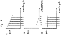
- FIGS. 4 are graphs for explaining a method to suppress the gain slope indicated in FIG. 3 (a) .
- FIG. 4(a) is a graph showing the gains at respective wavelengths before applying the VTEQ 11.
- the vertical axis represents gains at respective wavelengths.
- the horizontal axis represents the wavelength of each of signal beams composing a signal beam.
- a gain slope is represented by a dotted line.
- FIG. 4 (b) is a graph showing a loss slope derived from a gain slope value.
- the horizontal axis represents the wavelength of the signal beam; the vertical axis represents the loss to be given to each of signal beams of respective wavelengths; and a dotted line indicates the loss slope.
- FIG. 4(c) is a graph showing gains at the respective wavelengths after applying the VTEQ 11.
- the vertical axis represents gains at respective wavelengths.
- the horizontal axis represents the wavelength of each of signal beams composing a signal beam. Also, a dotted line indicates a gain slope.
- the tilt control unit 22 uses the gain slope characteristic shown in FIG. 2 to estimate a gain slope value corresponding to the target gain obtained from the excitation light control unit 21. That is to say, if the target gain is 18 [dB] as indicated at (a) of Fig.2 , the gain slope value can be estimated as (-0.4) [dBpp], whereby it can be estimated that the gain slope goes down to the right as shown in FIG. 4(a) .
- the VTEQ 11 is controlled by the tilt control unit 22, so that the VTEQ 11 gives signal beams the losses according to the loss slope indicated in FIG. 4(b) .
- this line segment is referred to as a loss slope, and the slope of the line segment is defined as a loss slope value for explanation.
- the VTEQ 11 attenuates signal beam power by a loss amount corresponding to the loss slope of each wavelength.
- a maximum loss is given to the gain at a shortest wavelength CH1 and a minimum loss is given to the gain at a longest wavelength CH5.
- Each of CH2 to CH4 is given a corresponding loss defined on a line segment passing a point corresponding to CH1 in FIG. 4(b) and a point corresponding to CH5 therein.
- the VTEQ 11 gives the signal beam, losses of the loss slope values each of which is a calculated gain slope value.
- the loss at CH5 should be preferably close to zero as shown in FIG. 4(b) .
- any loss is acceptable as long as the loss slope is obtained from the loss slope value corresponding to the gain slope value and the gains at respective wavelengths are to be flattened.
- the loss gain slope value is defined as gain slope value; however, the correspondence relation between the loss slope and the gain slope may be expressed as a formula or the correspondence relation may be stored as a data table obtained by measuring.
- the tilt control unit 22 may use the operating gain to control the VTEQ 11. Even in a case where the operating gain differs from the target gain, the gain slope value can be obtained accurately by using the operating gain.
- the LD 7a may be controlled so that the output signal beam power detected by the PD 6b will be within a setting range.
- the loss slope of the VTEQ 11 is adjusted according to the operating gain calculated from the input signal beam power using (Formula 1).
- a control time constant of the VTEQ 11 is set to be longer than a control time constant of the LD controlled by the excitation light control unit 21. It is because there is a limitation on a response speed when the loss slope of the VTEQ 11 is varied, and also because it is necessary to prevent failure in a stable convergence control, which is to be caused when the loss slope control competes with the control for varying the excitation light intensity of the LD.
- the optical amplifier 100 according to Embodiment 1 suppresses the gain slope by using the VTEQ 11; therefore, even with its simple configuration, the optical amplifier 100 can suppress the gain's wavelength-dependence.
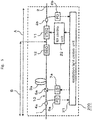
- FIG. 5 is a configuration diagram of an optical amplifier 200 according to Embodiment 2.
- a shape equalizer (SEQ) 12 is newly provided between the EDF 3a and the VTEQ 11.
- SEQ shape equalizer
- interval A indicated by a solid double arrow line is the same as that in FIG. 1 .
- Interval B indicated by another solid double arrow line is an interval between the beam input unit 1 and a downward broken line arrow.
- the downward broken line arrow indicates a portion between an output end of the SEQ 12 and an input end of the VTEQ 11. Interval A and interval B will be used later when comparing the optical amplifier 200 according to the present Embodiment with the conventional optical amplifier.
- the SEQ 12 is a component which has a loss characteristic to correct a non-linear characteristic portions that the VTEQ 11 cannot correct in the wavelength-dependence of the amplified-signal beam gain and that, so as to make the wavelength-dependence be linear. Whereas the loss slope of the tilt equalizer 11 is variable, the SEQ 12 has an inherent loss characteristic.
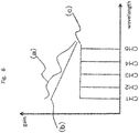
- FIG. 6 is an explanatory graph showing a gain slope suppression method using the VTEQ 11 and the SEQ 12.
- (a) indicates gains at respective wavelengths before the SEQ 12 is applied;
- (b) indicates gains at the respective wavelengths after the SEQ 12 is applied;
- (c) indicates gains at the respective wavelengths after the SEQ 12 and the VTEQ 11 are applied.
- the SEQ 12 corrects non-linear portions of the gain's wavelength-dependence so that the gain slope will become almost linear.
- (a) which includes non-linear components is varied to (b) which is almost linear.
- the VTEQ 11 decreases the gain slope as shown in (c) to make the gain slope flat.
- a diffraction grating such as a fiber grading, etalon filter, or dielectric multilayer filter is used.
- the VTEQ 11 suppresses the gain slope, and the non-linear components in the gain's wavelength-dependence are eliminated by the SEQ 12. Therefore, even if the gain's wavelength-dependence is not linear, the gain's wavelength-dependence can be suppressed.
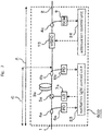
- FIG. 7 is a configuration diagram showing a conventional optical amplifier 600.
- a variable shape equalizer 13 (VSEQ) is provided instead of the VTEQ 11, and an optical splitter 4c and an OCM 8 are provided.
- a solid double arrow line A indicates an interval from the beam input unit 1 to the beam output unit 2.
- a solid double arrow line C indicates an interval from the beam input unit 1 to an input end (shown by a downward broken line arrow in the figure) of the VSEQ 13.
- An excitation light control unit 23 controls the LD 7a so that the average gain of the signal beam in interval C will become close to the target gain G1.
- the signal beam is split by the optical splitter 4c and inputted to the OCM 8.
- the OCM 8 measures power of a wavelength-multiplexed signal beam at individual wavelengths.
- the VSEQ 13 makes adjustment so that power levels at the respective wavelengths of the signal beam outputted from the beam output unit 2 will become the same.
- the attenuation control unit 24 controls the VSEQ 13 on the basis of the signal beam power levels obtained by the OCM 8 at the respective wavelengths so that each of the signal beam power levels at the respective wavelengths will become a same value.
- the conventional optical amplifier 600 shown in FIG. 7 has a problem that in a case where the wavelength-dependence of the EDF gains causes gain deviations between wavelengths, the gain deviations cause gain fluctuation at each wavelength when the number of wavelengths varies. The problem will be explained below in detail.
- FIG. 8 includes explanatory graphs showing control results when the conventional optical amplifier 600 is used.
- row (a1) shows a five-wavelength input state where a signal beam having five wavelengths of CH1 to CH5 is inputted
- row (b1) shows a single-wavelength input state.
- column (i) indicates average gains in interval C (illustrated in FIG. 7 ) which is the interval between the beam input unit 1 and the VSEQ 13; column (ii) indicates losses which the VSEQ 13 gives to the signal beam. Also, column (iii) indicates average gains in interval A (illustrated in FIG. 7 ) which is the interval between the beam input unit 1 and the beam output unit 2.
- horizontal broken lines indicate an externally-set target gain G1; and horizontal dash-dotted lines indicate G2 which is a gain of CH1 in interval C in the five-wavelength input state.
- row (a1) in FIG. 8 On the basis of the target gain G1, the excitation light control unit 23 controls the operating gain which is the average gain in interval C . Therefore, a graph in row (a1) of column (i) shows that the gain at CH3 almost agrees with the target gain G1. This is because, in the graph in FIG. 8 , the gain at CH3 almost agrees with an average gain of all the five wavelengths CH1 to CH5 in the signal beam, and also the average gain in interval C is controlled so as to become close to the target gain G1.
- a graph in column (iii) shows a state where, after passing the VSEQ 13, the gains at CH1 to CH5 are the same specific value. Because the VSEQ 13 is a component for giving losses, an operating gain G01 which is an average gain in interval A in the five-wavelength input state becomes lower than the target gain G1.
- the gain at CH1 is controlled so as to take the same value as the target gain G1. Therefore, as indicated by a solid downward arrow in the graph, the gain at CH1 decreases from G2.
- the average gain in interval A namely the operating gain, significantly decreases from G01 to G02 as shown in the graphs.
- the conventional optical amplifier 600 has a problem in that in a case where the number of wavelengths of the signal beam fluctuates, the operating gain significantly varies.
- the gain reduction can be compensated through adjustment of the VSEQ 13.
- the control of the VSEQ 13 is generally performed slower than the constant gain control performed by the EDF. This is due to a response speed limitation about an attenuating component used in the VSEQ 13.
- the response speed of the VSEQ 13 controlled by the attenuation control unit 24 is slow (a millisecond or more), and the response speed of the EDF 3a controlled by the excitation light control unit 23 is fast (a millisecond or less).
- the operating gain remains in a varied state, namely in a state where the signal beam power is deviated from the target gain.
- such deviation accumulates as the signal beam passes through a large number of optical amplifiers, causing degradation of communication quality. Consequently, in such an optical transmission system, a temporary degradation in communication quality is not acceptable; it is not acceptable that the communication quality is damaged until the VSEQ 13 completes adjustment.
- FIG. 9 includes explanatory graphs showing the control results when the optical amplifier 200 according to Embodiment 2 is used.
- Row (b1) shows a state where a signal beam having five wavelengths of CH1 to CH5 is inputted.
- Row (b2) shows a state where a signal beam having a single wavelength is inputted. Also, column (i) shows gains at CH1 to CH5 in interval B shown in FIG. 5 . Column (ii) shows losses given by the VTEQ 11. Also, column (iii) shows gains at CH1 to CH5 in interval A shown in FIG. 5 . In the figure, broken lines indicate an externally-set target gain G1.
- the operating gain G01 in interval A in the five-wavelength input state is the same as the operating gain G02 which is the average gain in the single-wavelength input state. That is, even when the number of wavelengths fluctuates, the average gain of the signal beam in interval A does not vary.
- This effect is achieved by a configuration which differs from that of the conventional optical amplifier 600 shown in FIG. 8 and in which the optical splitter 4b is provided not at the input side of the VTEQ 11 but at the output side thereof, and the PD 6b measures the signal beam power at the output side of the VTEQ 11.
- the optical amplifier 200 when the number of wavelengths in the signal beam varies from five to one, the optical amplifier 200 produces less fluctuation in the average gain in interval A than the conventional optical amplifier 600.
- the optical amplifier 200 has a configuration in which the PD 6b for measuring the signal beam power is not arranged at the input side of the VTEQ 11 but is properly arranged at the output side thereof, and in which instead of the VSEQ 13 for uniforming signal beam power at each wavelength, the VTEQ 11 is used for making the respective gains equal between wavelengths.
- the operating gain G01 in interval A in the five-wavelength input state varies little, from the operating gain G02 in the single-wavelength input state. That is to say, when the number of wavelengths fluctuates, a proper control can be performed in which the gain's wavelength-dependence is suppressed and the significant fluctuation of the operating gain is suppressed.
- the communication quality can be maintained stable.
- the conventional optical amplifier 600 As described above, in the conventional optical amplifier 600, the constant gain control method and the method for suppressing gain deviation between wavelengths are introduced; therefore, the conventional optical amplifier 600 is generally at an acceptable level for a desired operation and performance. However, detailed analysis into the operation reveals that constant gain control with sufficiently high accuracy has not exactly been realized.
- the optical amplifier 200 according to Embodiment 2 of the present invention realizes a constant gain control with high accuracy on the basis of accurate analysis. Furthermore, even in a case where the gain's wavelength-dependence occurs, the optical amplifier 200 can maintain flatness in gains among respective wavelengths without using an excitation light source with excessively high output power and high cost, which thereby realizes a highly-accurate constant gain control.
- the optical splitter 4b is properly arranged at the output side of the VTEQ 11 to perform constant gain control using the output-side signal beam power measured by the PD 6b and to make gains equal between different wavelengths of the signal beam instead of uniforming power at different wavelengths of the signal beam. This can perform proper control even in a case where the number of wavelengths fluctuates.
- FIG. 10 is a configuration diagram of an optical amplifier 300 according to Embodiment 3.
- the optical amplifier 300 according to Embodiment 3 is different in that a wavelength-selective optical coupler 5b serving as a second optical coupling unit and an LD 7b are provided at a stage subsequent to the EDF 3a.
- the LD 7b excites the EDF 3a at the stage subsequent to the EDF 3a.
- the SEQ 12 may be provided between the wavelength-selective optical coupler 5b and the VTEQ 11.
- FIG. 11 is a configuration diagram of an optical amplifier 400 according to Embodiment 4.
- an LD 7b as an excitation light source and a wavelength-selective optical coupler 5b are further provided at a stage subsequent to the EDF 3a.
- the EDF 3a is excited from both of the prior and subsequent stages.
- a SEQ 12 may be provided between the wavelength-selective optical coupler 5b and the VTEQ 11.
- components which are the same as or correspond to those shown in FIG. 1 are given the same symbols and the description therefor will be omitted.
- FIG. 12 is a configuration diagram of an optical amplifier 500 according to Embodiment 5.
- the optical amplifier 500 according to Embodiment 5 is different in that an EDF 3b serving as a second beam amplification unit is further provided at a stage prior to the VTEQ 11, and instead of the wavelength-selective optical coupler 5b, a wavelength-selective optical coupler 5c serving as a third optical coupling unit is provided between the EDFs 3a and 3b.
- the LD 7b performs forward excitation of the EDF 3b through the wavelength-selective optical coupler 5c.
- a SEQ 12 may be provided between the wavelength-selective optical coupler 5c and the VTEQ 11.
- components which are the same as or correspond to those shown in FIG. 11 are given the same symbols and the description will be omitted.
- VTEQs are used for suppressing the wavelength-dependence of EDFs
- the gain of the EDF is fixed to a specific value that produces no wavelength-dependence.
- the EDF is to be initially excited so that the gain will have no wavelength-dependence, and then, attenuated down to the required gain.
- This configuration requires a high-output and expensive excitation light source, making the optical amplifier more expensive and excessively power-consuming.
- the input signal beam power of the optical amplifier and the output signal beam power thereof are measured and the excitation light intensity of the excitation light source is controlled so that the optical amplifier gain will become equal to the target gain.
- the amplified-signal beam power is measured right after the beam amplification unit, so that the excitation light intensity of excitation light source is controlled using the input signal beam power and the amplified-signal beam power, and then the gain's wavelength-dependence is suppressed.
- the suppression of the gain's wavelength-dependence causes attenuation of the signal beam, making the optical amplifier gain lowered than the target gain.
- the optical amplifier of the present invention can suppress the fluctuation of the gain more effectively than the conventional optical amplifier and, even when the number of the wavelengths decreases, the communication quality can be maintained stable. It is needless to say that this effect can be achieved not only with the configuration of Embodiment 2, but also with any configuration described in Embodiment 1 or Embodiments 3 to 5 of the present invention.
- any configuration produced by combining these embodiments may be used. Also, it is needless to say that a configuration obtained by combining the embodiments may be properly modified to configure an optical amplifier.
Landscapes
- Physics & Mathematics (AREA)
- Electromagnetism (AREA)
- Engineering & Computer Science (AREA)
- Plasma & Fusion (AREA)
- Optics & Photonics (AREA)
- Computer Networks & Wireless Communication (AREA)
- Signal Processing (AREA)
- Automation & Control Theory (AREA)
- Lasers (AREA)
Applications Claiming Priority (1)
| Application Number | Priority Date | Filing Date | Title |
|---|---|---|---|
| PCT/JP2015/082484 WO2017085822A1 (fr) | 2015-11-19 | 2015-11-19 | Amplificateur optique |
Publications (3)
| Publication Number | Publication Date |
|---|---|
| EP3379662A1 true EP3379662A1 (fr) | 2018-09-26 |
| EP3379662A4 EP3379662A4 (fr) | 2018-12-05 |
| EP3379662B1 EP3379662B1 (fr) | 2025-04-09 |
Family
ID=58718625
Family Applications (1)
| Application Number | Title | Priority Date | Filing Date |
|---|---|---|---|
| EP15908762.6A Active EP3379662B1 (fr) | 2015-11-19 | 2015-11-19 | Amplificateur optique |
Country Status (5)
| Country | Link |
|---|---|
| US (1) | US10971888B2 (fr) |
| EP (1) | EP3379662B1 (fr) |
| JP (1) | JPWO2017085822A1 (fr) |
| CN (1) | CN108352672A (fr) |
| WO (1) | WO2017085822A1 (fr) |
Cited By (1)
| Publication number | Priority date | Publication date | Assignee | Title |
|---|---|---|---|---|
| EP3952142A4 (fr) * | 2019-03-25 | 2022-05-25 | NEC Corporation | Égaliseur optique, procédé et support non transitoire lisible par ordinateur |
Families Citing this family (2)
| Publication number | Priority date | Publication date | Assignee | Title |
|---|---|---|---|---|
| CN110601766B (zh) * | 2019-09-10 | 2020-11-13 | 武汉光迅科技股份有限公司 | 一种控制方法及光纤放大器 |
| US20240258758A1 (en) * | 2023-01-26 | 2024-08-01 | Fujitsu Limited | Optical signal amplification |
Family Cites Families (18)
| Publication number | Priority date | Publication date | Assignee | Title |
|---|---|---|---|---|
| JP3306700B2 (ja) | 1996-05-02 | 2002-07-24 | 富士通株式会社 | 光増幅装置及び波長多重光伝送システム |
| US6728026B2 (en) * | 1998-07-14 | 2004-04-27 | Novera Optics, Inc. | Dynamically tunable optical amplifier and fiber optic light source |
| JP3844902B2 (ja) * | 1999-03-02 | 2006-11-15 | 富士通株式会社 | 波長多重用光増幅器及び光通信システム |
| US6456428B1 (en) * | 1999-09-02 | 2002-09-24 | Sumitomo Electric Industries, Ltd. | Optical amplifier |
| US6535329B1 (en) * | 1999-12-20 | 2003-03-18 | Jds Uniphase Inc. | Temperature tuning an optical amplifier |
| EP1130819A1 (fr) | 2000-03-03 | 2001-09-05 | Telefonaktiebolaget Lm Ericsson | Détermination de la pente de gain d'amplificateurs optiques par la mesure du gain total |
| US6731424B1 (en) * | 2001-03-15 | 2004-05-04 | Onetta, Inc. | Dynamic gain flattening in an optical communication system |
| US6611371B2 (en) | 2001-03-16 | 2003-08-26 | Corning Incorporated | Single parameter gain slope adjuster for an optical system |
| US6535330B1 (en) * | 2001-03-31 | 2003-03-18 | Corning Incorporated | Dynamic controller for a multi-channel optical amplifier |
| US6483631B1 (en) * | 2001-06-05 | 2002-11-19 | Onetta, Inc. | Optical amplifier spectral tilt controllers |
| GB0124258D0 (en) | 2001-10-09 | 2001-11-28 | Marconi Comm Ltd | Optical amplifier control in WDM communications systems |
| JP3903830B2 (ja) * | 2002-04-05 | 2007-04-11 | 株式会社日立製作所 | 利得補償装置及びそれを用いた伝送システム |
| JP3551418B2 (ja) | 2003-05-27 | 2004-08-04 | 富士通株式会社 | 光伝送装置及び波長多重光通信システム |
| JP4298570B2 (ja) * | 2004-04-13 | 2009-07-22 | 富士通株式会社 | 光ファイバ増幅器の制御方法および光伝送システム |
| JP2006108499A (ja) | 2004-10-07 | 2006-04-20 | Furukawa Electric Co Ltd:The | 光信号増幅装置及びロススペクトルの決定方法。 |
| JP2006286918A (ja) * | 2005-03-31 | 2006-10-19 | Furukawa Electric Co Ltd:The | 光増幅装置 |
| US8233214B2 (en) * | 2008-02-13 | 2012-07-31 | Maxim Bolshtyansky | Optical fiber amplifier and a control method therefor |
| JP2012156285A (ja) * | 2011-01-26 | 2012-08-16 | Fujitsu Ltd | 光増幅装置 |
-
2015
- 2015-11-19 US US15/774,019 patent/US10971888B2/en active Active
- 2015-11-19 WO PCT/JP2015/082484 patent/WO2017085822A1/fr not_active Ceased
- 2015-11-19 CN CN201580084532.0A patent/CN108352672A/zh active Pending
- 2015-11-19 EP EP15908762.6A patent/EP3379662B1/fr active Active
- 2015-11-19 JP JP2017551453A patent/JPWO2017085822A1/ja active Pending
Cited By (1)
| Publication number | Priority date | Publication date | Assignee | Title |
|---|---|---|---|---|
| EP3952142A4 (fr) * | 2019-03-25 | 2022-05-25 | NEC Corporation | Égaliseur optique, procédé et support non transitoire lisible par ordinateur |
Also Published As
| Publication number | Publication date |
|---|---|
| US20180358775A1 (en) | 2018-12-13 |
| EP3379662A4 (fr) | 2018-12-05 |
| CN108352672A (zh) | 2018-07-31 |
| WO2017085822A1 (fr) | 2017-05-26 |
| JPWO2017085822A1 (ja) | 2018-06-28 |
| EP3379662B1 (fr) | 2025-04-09 |
| US10971888B2 (en) | 2021-04-06 |
Similar Documents
| Publication | Publication Date | Title |
|---|---|---|
| US7715092B2 (en) | Dynamic raman tilt compensation | |
| JP3527627B2 (ja) | 光ファイバ増幅器 | |
| US7898732B2 (en) | Fast dynamic gain control in a bidirectionally-pumped Raman fiber amplifier | |
| US7554719B2 (en) | Fast dynamic gain control in an optical fiber amplifier | |
| US7142356B2 (en) | Fast dynamic gain control in an optical fiber amplifier | |
| EP3379662B1 (fr) | Amplificateur optique | |
| WO2004077700A1 (fr) | Controleur d'amplificateur de raman a pompage a plusieurs longueurs d'onde, procede de controle, et programme de controle | |
| JP2002208758A (ja) | 光増幅装置 | |
| JP2001094181A (ja) | 光増幅器 | |
| US7400444B2 (en) | Optical amplifier and control method for optical amplifier | |
| JP4337545B2 (ja) | 光通信システム | |
| EP1696524B1 (fr) | Contrôle rapide de gain dynamique dans un amplificateur à fibre optique | |
| JP3811134B2 (ja) | 光増幅器 | |
| US20070109628A1 (en) | Fast Dynamic Gain Control in Cascaded Raman Fiber Amplifiers | |
| US20080088915A1 (en) | Optical amplification characteristics simulation apparatus and optical amplification characteristics simulation method | |
| US8379299B2 (en) | Optical amplifier | |
| JP2006286918A (ja) | 光増幅装置 | |
| US20070109623A1 (en) | Fast Dynamic Gain Control in a Bidirectionally-Pumped Raman Fiber Amplifier | |
| US7280269B2 (en) | Fast dynamic gain control in cascaded Raman fiber amplifiers | |
| US7280271B2 (en) | Fast dynamic gain control in cascaded Raman fiber amplifiers | |
| JP3902214B2 (ja) | 光伝送装置 | |
| JP2001308421A (ja) | 光ファイバ増幅器の特性評価方法及び特性評価装置、ならびに波長多重光増幅装置及び波長多重光伝送装置 | |
| US20070109625A1 (en) | Fast Dynamic Gain Control in Cascaded Raman Fiber Amplifiers | |
| HK1092596B (en) | Fast dynamic gain control in an optical fiber amplifier |
Legal Events
| Date | Code | Title | Description |
|---|---|---|---|
| STAA | Information on the status of an ep patent application or granted ep patent |
Free format text: STATUS: THE INTERNATIONAL PUBLICATION HAS BEEN MADE |
|
| PUAI | Public reference made under article 153(3) epc to a published international application that has entered the european phase |
Free format text: ORIGINAL CODE: 0009012 |
|
| STAA | Information on the status of an ep patent application or granted ep patent |
Free format text: STATUS: REQUEST FOR EXAMINATION WAS MADE |
|
| 17P | Request for examination filed |
Effective date: 20180515 |
|
| AK | Designated contracting states |
Kind code of ref document: A1 Designated state(s): AL AT BE BG CH CY CZ DE DK EE ES FI FR GB GR HR HU IE IS IT LI LT LU LV MC MK MT NL NO PL PT RO RS SE SI SK SM TR |
|
| AX | Request for extension of the european patent |
Extension state: BA ME |
|
| A4 | Supplementary search report drawn up and despatched |
Effective date: 20181029 |
|
| RIC1 | Information provided on ipc code assigned before grant |
Ipc: H04B 10/296 20130101ALN20181023BHEP Ipc: H01S 3/10 20060101AFI20181023BHEP Ipc: H01S 3/067 20060101ALN20181023BHEP Ipc: H01S 3/0941 20060101ALN20181023BHEP Ipc: H01S 3/094 20060101ALN20181023BHEP Ipc: H04B 10/077 20130101ALN20181023BHEP Ipc: H04B 10/293 20130101ALN20181023BHEP Ipc: H01S 3/13 20060101ALI20181023BHEP Ipc: H01S 3/00 20060101ALN20181023BHEP Ipc: H01S 3/16 20060101ALN20181023BHEP |
|
| DAV | Request for validation of the european patent (deleted) | ||
| DAX | Request for extension of the european patent (deleted) | ||
| STAA | Information on the status of an ep patent application or granted ep patent |
Free format text: STATUS: EXAMINATION IS IN PROGRESS |
|
| 17Q | First examination report despatched |
Effective date: 20200420 |
|
| GRAP | Despatch of communication of intention to grant a patent |
Free format text: ORIGINAL CODE: EPIDOSNIGR1 |
|
| STAA | Information on the status of an ep patent application or granted ep patent |
Free format text: STATUS: GRANT OF PATENT IS INTENDED |
|
| RIC1 | Information provided on ipc code assigned before grant |
Ipc: H04B 10/294 20130101ALI20241104BHEP Ipc: H01S 3/16 20060101ALI20241104BHEP Ipc: H01S 3/0941 20060101ALI20241104BHEP Ipc: H01S 3/094 20060101ALI20241104BHEP Ipc: H01S 3/067 20060101ALI20241104BHEP Ipc: H01S 3/00 20060101ALI20241104BHEP Ipc: H01S 3/13 20060101ALI20241104BHEP Ipc: H01S 3/10 20060101AFI20241104BHEP |
|
| INTG | Intention to grant announced |
Effective date: 20241204 |
|
| GRAS | Grant fee paid |
Free format text: ORIGINAL CODE: EPIDOSNIGR3 |
|
| GRAA | (expected) grant |
Free format text: ORIGINAL CODE: 0009210 |
|
| STAA | Information on the status of an ep patent application or granted ep patent |
Free format text: STATUS: THE PATENT HAS BEEN GRANTED |
|
| AK | Designated contracting states |
Kind code of ref document: B1 Designated state(s): AL AT BE BG CH CY CZ DE DK EE ES FI FR GB GR HR HU IE IS IT LI LT LU LV MC MK MT NL NO PL PT RO RS SE SI SK SM TR |
|
| REG | Reference to a national code |
Ref country code: GB Ref legal event code: FG4D |
|
| REG | Reference to a national code |
Ref country code: CH Ref legal event code: EP |
|
| REG | Reference to a national code |
Ref country code: DE Ref legal event code: R096 Ref document number: 602015091426 Country of ref document: DE |
|
| REG | Reference to a national code |
Ref country code: IE Ref legal event code: FG4D |
|
| REG | Reference to a national code |
Ref country code: NL Ref legal event code: MP Effective date: 20250409 |
|
| PG25 | Lapsed in a contracting state [announced via postgrant information from national office to epo] |
Ref country code: NL Free format text: LAPSE BECAUSE OF FAILURE TO SUBMIT A TRANSLATION OF THE DESCRIPTION OR TO PAY THE FEE WITHIN THE PRESCRIBED TIME-LIMIT Effective date: 20250409 |
|
| REG | Reference to a national code |
Ref country code: AT Ref legal event code: MK05 Ref document number: 1784434 Country of ref document: AT Kind code of ref document: T Effective date: 20250409 |
|
| PG25 | Lapsed in a contracting state [announced via postgrant information from national office to epo] |
Ref country code: PT Free format text: LAPSE BECAUSE OF FAILURE TO SUBMIT A TRANSLATION OF THE DESCRIPTION OR TO PAY THE FEE WITHIN THE PRESCRIBED TIME-LIMIT Effective date: 20250811 Ref country code: FI Free format text: LAPSE BECAUSE OF FAILURE TO SUBMIT A TRANSLATION OF THE DESCRIPTION OR TO PAY THE FEE WITHIN THE PRESCRIBED TIME-LIMIT Effective date: 20250409 Ref country code: ES Free format text: LAPSE BECAUSE OF FAILURE TO SUBMIT A TRANSLATION OF THE DESCRIPTION OR TO PAY THE FEE WITHIN THE PRESCRIBED TIME-LIMIT Effective date: 20250409 |
|
| REG | Reference to a national code |
Ref country code: LT Ref legal event code: MG9D |
|
| PG25 | Lapsed in a contracting state [announced via postgrant information from national office to epo] |
Ref country code: GR Free format text: LAPSE BECAUSE OF FAILURE TO SUBMIT A TRANSLATION OF THE DESCRIPTION OR TO PAY THE FEE WITHIN THE PRESCRIBED TIME-LIMIT Effective date: 20250710 Ref country code: NO Free format text: LAPSE BECAUSE OF FAILURE TO SUBMIT A TRANSLATION OF THE DESCRIPTION OR TO PAY THE FEE WITHIN THE PRESCRIBED TIME-LIMIT Effective date: 20250709 |
|
| PG25 | Lapsed in a contracting state [announced via postgrant information from national office to epo] |
Ref country code: PL Free format text: LAPSE BECAUSE OF FAILURE TO SUBMIT A TRANSLATION OF THE DESCRIPTION OR TO PAY THE FEE WITHIN THE PRESCRIBED TIME-LIMIT Effective date: 20250409 |
|
| PG25 | Lapsed in a contracting state [announced via postgrant information from national office to epo] |
Ref country code: BG Free format text: LAPSE BECAUSE OF FAILURE TO SUBMIT A TRANSLATION OF THE DESCRIPTION OR TO PAY THE FEE WITHIN THE PRESCRIBED TIME-LIMIT Effective date: 20250409 |
|
| PG25 | Lapsed in a contracting state [announced via postgrant information from national office to epo] |
Ref country code: HR Free format text: LAPSE BECAUSE OF FAILURE TO SUBMIT A TRANSLATION OF THE DESCRIPTION OR TO PAY THE FEE WITHIN THE PRESCRIBED TIME-LIMIT Effective date: 20250409 |
|
| PG25 | Lapsed in a contracting state [announced via postgrant information from national office to epo] |
Ref country code: AT Free format text: LAPSE BECAUSE OF FAILURE TO SUBMIT A TRANSLATION OF THE DESCRIPTION OR TO PAY THE FEE WITHIN THE PRESCRIBED TIME-LIMIT Effective date: 20250409 |
|
| PGFP | Annual fee paid to national office [announced via postgrant information from national office to epo] |
Ref country code: FR Payment date: 20250930 Year of fee payment: 11 |
|
| PG25 | Lapsed in a contracting state [announced via postgrant information from national office to epo] |
Ref country code: RS Free format text: LAPSE BECAUSE OF FAILURE TO SUBMIT A TRANSLATION OF THE DESCRIPTION OR TO PAY THE FEE WITHIN THE PRESCRIBED TIME-LIMIT Effective date: 20250709 |
|
| PG25 | Lapsed in a contracting state [announced via postgrant information from national office to epo] |
Ref country code: IS Free format text: LAPSE BECAUSE OF FAILURE TO SUBMIT A TRANSLATION OF THE DESCRIPTION OR TO PAY THE FEE WITHIN THE PRESCRIBED TIME-LIMIT Effective date: 20250809 |
|
| PG25 | Lapsed in a contracting state [announced via postgrant information from national office to epo] |
Ref country code: LV Free format text: LAPSE BECAUSE OF FAILURE TO SUBMIT A TRANSLATION OF THE DESCRIPTION OR TO PAY THE FEE WITHIN THE PRESCRIBED TIME-LIMIT Effective date: 20250409 |
|
| PGFP | Annual fee paid to national office [announced via postgrant information from national office to epo] |
Ref country code: DE Payment date: 20250930 Year of fee payment: 11 |
|
| REG | Reference to a national code |
Ref country code: DE Ref legal event code: R097 Ref document number: 602015091426 Country of ref document: DE |
|
| PG25 | Lapsed in a contracting state [announced via postgrant information from national office to epo] |
Ref country code: SM Free format text: LAPSE BECAUSE OF FAILURE TO SUBMIT A TRANSLATION OF THE DESCRIPTION OR TO PAY THE FEE WITHIN THE PRESCRIBED TIME-LIMIT Effective date: 20250409 Ref country code: DK Free format text: LAPSE BECAUSE OF FAILURE TO SUBMIT A TRANSLATION OF THE DESCRIPTION OR TO PAY THE FEE WITHIN THE PRESCRIBED TIME-LIMIT Effective date: 20250409 |
|
| PG25 | Lapsed in a contracting state [announced via postgrant information from national office to epo] |
Ref country code: CZ Free format text: LAPSE BECAUSE OF FAILURE TO SUBMIT A TRANSLATION OF THE DESCRIPTION OR TO PAY THE FEE WITHIN THE PRESCRIBED TIME-LIMIT Effective date: 20250409 |
|
| PG25 | Lapsed in a contracting state [announced via postgrant information from national office to epo] |
Ref country code: EE Free format text: LAPSE BECAUSE OF FAILURE TO SUBMIT A TRANSLATION OF THE DESCRIPTION OR TO PAY THE FEE WITHIN THE PRESCRIBED TIME-LIMIT Effective date: 20250409 |
|
| PG25 | Lapsed in a contracting state [announced via postgrant information from national office to epo] |
Ref country code: SK Free format text: LAPSE BECAUSE OF FAILURE TO SUBMIT A TRANSLATION OF THE DESCRIPTION OR TO PAY THE FEE WITHIN THE PRESCRIBED TIME-LIMIT Effective date: 20250409 |
|
| PG25 | Lapsed in a contracting state [announced via postgrant information from national office to epo] |
Ref country code: IT Free format text: LAPSE BECAUSE OF FAILURE TO SUBMIT A TRANSLATION OF THE DESCRIPTION OR TO PAY THE FEE WITHIN THE PRESCRIBED TIME-LIMIT Effective date: 20250409 |
|
| PLBE | No opposition filed within time limit |
Free format text: ORIGINAL CODE: 0009261 |
|
| STAA | Information on the status of an ep patent application or granted ep patent |
Free format text: STATUS: NO OPPOSITION FILED WITHIN TIME LIMIT |
|
| REG | Reference to a national code |
Ref country code: CH Ref legal event code: L10 Free format text: ST27 STATUS EVENT CODE: U-0-0-L10-L00 (AS PROVIDED BY THE NATIONAL OFFICE) Effective date: 20260218 |
|
| PG25 | Lapsed in a contracting state [announced via postgrant information from national office to epo] |
Ref country code: RO Free format text: LAPSE BECAUSE OF FAILURE TO SUBMIT A TRANSLATION OF THE DESCRIPTION OR TO PAY THE FEE WITHIN THE PRESCRIBED TIME-LIMIT Effective date: 20250409 |
|
| 26N | No opposition filed |
Effective date: 20260112 |