EP3380889B1 - Gebogene anzeigetafel und gebogene anzeigevorrichtung - Google Patents
Gebogene anzeigetafel und gebogene anzeigevorrichtung Download PDFInfo
- Publication number
- EP3380889B1 EP3380889B1 EP16852870.1A EP16852870A EP3380889B1 EP 3380889 B1 EP3380889 B1 EP 3380889B1 EP 16852870 A EP16852870 A EP 16852870A EP 3380889 B1 EP3380889 B1 EP 3380889B1
- Authority
- EP
- European Patent Office
- Prior art keywords
- domain
- subpixel
- branches
- black matrix
- region
- Prior art date
- Legal status (The legal status is an assumption and is not a legal conclusion. Google has not performed a legal analysis and makes no representation as to the accuracy of the status listed.)
- Active
Links
Images



Classifications
-
- G—PHYSICS
- G02—OPTICS
- G02F—OPTICAL DEVICES OR ARRANGEMENTS FOR THE CONTROL OF LIGHT BY MODIFICATION OF THE OPTICAL PROPERTIES OF THE MEDIA OF THE ELEMENTS INVOLVED THEREIN; NON-LINEAR OPTICS; FREQUENCY-CHANGING OF LIGHT; OPTICAL LOGIC ELEMENTS; OPTICAL ANALOGUE/DIGITAL CONVERTERS
- G02F1/00—Devices or arrangements for the control of the intensity, colour, phase, polarisation or direction of light arriving from an independent light source, e.g. switching, gating or modulating; Non-linear optics
- G02F1/01—Devices or arrangements for the control of the intensity, colour, phase, polarisation or direction of light arriving from an independent light source, e.g. switching, gating or modulating; Non-linear optics for the control of the intensity, phase, polarisation or colour
- G02F1/13—Devices or arrangements for the control of the intensity, colour, phase, polarisation or direction of light arriving from an independent light source, e.g. switching, gating or modulating; Non-linear optics for the control of the intensity, phase, polarisation or colour based on liquid crystals, e.g. single liquid crystal display cells
- G02F1/133—Constructional arrangements; Operation of liquid crystal cells; Circuit arrangements
- G02F1/1333—Constructional arrangements; Manufacturing methods
- G02F1/1343—Electrodes
- G02F1/134309—Electrodes characterised by their geometrical arrangement
- G02F1/134336—Matrix
-
- G—PHYSICS
- G02—OPTICS
- G02F—OPTICAL DEVICES OR ARRANGEMENTS FOR THE CONTROL OF LIGHT BY MODIFICATION OF THE OPTICAL PROPERTIES OF THE MEDIA OF THE ELEMENTS INVOLVED THEREIN; NON-LINEAR OPTICS; FREQUENCY-CHANGING OF LIGHT; OPTICAL LOGIC ELEMENTS; OPTICAL ANALOGUE/DIGITAL CONVERTERS
- G02F1/00—Devices or arrangements for the control of the intensity, colour, phase, polarisation or direction of light arriving from an independent light source, e.g. switching, gating or modulating; Non-linear optics
- G02F1/01—Devices or arrangements for the control of the intensity, colour, phase, polarisation or direction of light arriving from an independent light source, e.g. switching, gating or modulating; Non-linear optics for the control of the intensity, phase, polarisation or colour
- G02F1/13—Devices or arrangements for the control of the intensity, colour, phase, polarisation or direction of light arriving from an independent light source, e.g. switching, gating or modulating; Non-linear optics for the control of the intensity, phase, polarisation or colour based on liquid crystals, e.g. single liquid crystal display cells
- G02F1/133—Constructional arrangements; Operation of liquid crystal cells; Circuit arrangements
- G02F1/1333—Constructional arrangements; Manufacturing methods
- G02F1/1335—Structural association of cells with optical devices, e.g. polarisers or reflectors
- G02F1/133509—Filters, e.g. light shielding masks
- G02F1/133512—Light shielding layers, e.g. black matrix
-
- G—PHYSICS
- G02—OPTICS
- G02F—OPTICAL DEVICES OR ARRANGEMENTS FOR THE CONTROL OF LIGHT BY MODIFICATION OF THE OPTICAL PROPERTIES OF THE MEDIA OF THE ELEMENTS INVOLVED THEREIN; NON-LINEAR OPTICS; FREQUENCY-CHANGING OF LIGHT; OPTICAL LOGIC ELEMENTS; OPTICAL ANALOGUE/DIGITAL CONVERTERS
- G02F1/00—Devices or arrangements for the control of the intensity, colour, phase, polarisation or direction of light arriving from an independent light source, e.g. switching, gating or modulating; Non-linear optics
- G02F1/01—Devices or arrangements for the control of the intensity, colour, phase, polarisation or direction of light arriving from an independent light source, e.g. switching, gating or modulating; Non-linear optics for the control of the intensity, phase, polarisation or colour
- G02F1/13—Devices or arrangements for the control of the intensity, colour, phase, polarisation or direction of light arriving from an independent light source, e.g. switching, gating or modulating; Non-linear optics for the control of the intensity, phase, polarisation or colour based on liquid crystals, e.g. single liquid crystal display cells
- G02F1/133—Constructional arrangements; Operation of liquid crystal cells; Circuit arrangements
- G02F1/1333—Constructional arrangements; Manufacturing methods
- G02F1/1343—Electrodes
- G02F1/134309—Electrodes characterised by their geometrical arrangement
-
- G—PHYSICS
- G02—OPTICS
- G02F—OPTICAL DEVICES OR ARRANGEMENTS FOR THE CONTROL OF LIGHT BY MODIFICATION OF THE OPTICAL PROPERTIES OF THE MEDIA OF THE ELEMENTS INVOLVED THEREIN; NON-LINEAR OPTICS; FREQUENCY-CHANGING OF LIGHT; OPTICAL LOGIC ELEMENTS; OPTICAL ANALOGUE/DIGITAL CONVERTERS
- G02F1/00—Devices or arrangements for the control of the intensity, colour, phase, polarisation or direction of light arriving from an independent light source, e.g. switching, gating or modulating; Non-linear optics
- G02F1/01—Devices or arrangements for the control of the intensity, colour, phase, polarisation or direction of light arriving from an independent light source, e.g. switching, gating or modulating; Non-linear optics for the control of the intensity, phase, polarisation or colour
- G02F1/13—Devices or arrangements for the control of the intensity, colour, phase, polarisation or direction of light arriving from an independent light source, e.g. switching, gating or modulating; Non-linear optics for the control of the intensity, phase, polarisation or colour based on liquid crystals, e.g. single liquid crystal display cells
- G02F1/133—Constructional arrangements; Operation of liquid crystal cells; Circuit arrangements
- G02F1/1333—Constructional arrangements; Manufacturing methods
- G02F1/1343—Electrodes
- G02F1/13439—Electrodes characterised by their electrical, optical, physical properties; materials therefor; method of making
-
- G—PHYSICS
- G02—OPTICS
- G02F—OPTICAL DEVICES OR ARRANGEMENTS FOR THE CONTROL OF LIGHT BY MODIFICATION OF THE OPTICAL PROPERTIES OF THE MEDIA OF THE ELEMENTS INVOLVED THEREIN; NON-LINEAR OPTICS; FREQUENCY-CHANGING OF LIGHT; OPTICAL LOGIC ELEMENTS; OPTICAL ANALOGUE/DIGITAL CONVERTERS
- G02F1/00—Devices or arrangements for the control of the intensity, colour, phase, polarisation or direction of light arriving from an independent light source, e.g. switching, gating or modulating; Non-linear optics
- G02F1/01—Devices or arrangements for the control of the intensity, colour, phase, polarisation or direction of light arriving from an independent light source, e.g. switching, gating or modulating; Non-linear optics for the control of the intensity, phase, polarisation or colour
- G02F1/13—Devices or arrangements for the control of the intensity, colour, phase, polarisation or direction of light arriving from an independent light source, e.g. switching, gating or modulating; Non-linear optics for the control of the intensity, phase, polarisation or colour based on liquid crystals, e.g. single liquid crystal display cells
- G02F1/133—Constructional arrangements; Operation of liquid crystal cells; Circuit arrangements
- G02F1/1333—Constructional arrangements; Manufacturing methods
- G02F1/1343—Electrodes
- G02F1/134309—Electrodes characterised by their geometrical arrangement
- G02F1/134345—Subdivided pixels, e.g. for grey scale or redundancy
-
- G—PHYSICS
- G02—OPTICS
- G02F—OPTICAL DEVICES OR ARRANGEMENTS FOR THE CONTROL OF LIGHT BY MODIFICATION OF THE OPTICAL PROPERTIES OF THE MEDIA OF THE ELEMENTS INVOLVED THEREIN; NON-LINEAR OPTICS; FREQUENCY-CHANGING OF LIGHT; OPTICAL LOGIC ELEMENTS; OPTICAL ANALOGUE/DIGITAL CONVERTERS
- G02F2201/00—Constructional arrangements not provided for in groups G02F1/00 - G02F7/00
- G02F2201/12—Constructional arrangements not provided for in groups G02F1/00 - G02F7/00 electrode
- G02F2201/123—Constructional arrangements not provided for in groups G02F1/00 - G02F7/00 electrode pixel
-
- G—PHYSICS
- G02—OPTICS
- G02F—OPTICAL DEVICES OR ARRANGEMENTS FOR THE CONTROL OF LIGHT BY MODIFICATION OF THE OPTICAL PROPERTIES OF THE MEDIA OF THE ELEMENTS INVOLVED THEREIN; NON-LINEAR OPTICS; FREQUENCY-CHANGING OF LIGHT; OPTICAL LOGIC ELEMENTS; OPTICAL ANALOGUE/DIGITAL CONVERTERS
- G02F2203/00—Function characteristic
- G02F2203/64—Normally black display, i.e. the off state being black
Definitions
- the present invention relates to display technology, more particularly, to a curved display panel and a curved display apparatus.
- the present invention provides a curved display panel as defined in claim 1.
- the present invention provides a curved display apparatus as defined in claim 2.
- the display panel is curved with respect to an axis.
- the array substrate and the counter substrate in the display panel offset from each other.
- the black matrix layer is designed to be large enough to compensate the offset.
- the array substrate shifts away from the counter substrate towards two different directions with respect to the axis.
- the black matrix layer patterns are different on two different sides of the curved display apparatus. Typically, the black matrix layer on both sides is designed to be large enough to at least cover any offset between the array substrate and the counter substrate.
- the black matrix layer is disposed on the counter substrate, with each black matrix opening aligned with the center of a pixel electrode.
- the black matrix opening is not aligned with the center of the corresponding pixel electrode, resulting in a loss of aperture ration.
- the black matrix layer is disposed on the array substrate.
- the color filter on the counter substrate is not aligned with a corresponding pixel electrode, affecting display quality.
- FIG. 1 is a diagram illustrating the structure of a display panel in a conventional curved display apparatus.
- the pixel electrode in the display panel has a rectangular shape.
- the display panel is curved with respect to an axis L.
- each rectangular shaped pixel electrode has a long side and a short side.
- the long side has a length d
- the short side has a width w.
- the rectangular shaped pixel electrodes are arranged so that a long side of each rectangular shaped pixel electrode is parallel to the axis L.
- each pixel electrode is shifted relative to the counter substrate by a distance ⁇ w.
- each pixel electrode is offset with respect to the counter substrate by an offset region (see the shaded region in FIG. 1 ).
- the offset region has an area of ⁇ w ⁇ d.
- the offset region has a relatively large area, affecting display quality in the conventional curved display apparatus.
- the present invention provides, inter alia, a curved display panel and a curved display apparatus that substantially obviate one or more of the problems due to limitations and disadvantages of the related art.
- the present disclosure provides a curved display panel having an array substrate including an array of subpixels arranged in rows and columns.
- the curved display panel is curved with respect to an axis substantially parallel to the column direction.
- the array substrate includes a plurality of pixel electrodes corresponding to the array of subpixels; each of the plurality of pixel electrodes is in a subpixel and has a first dimension along a row direction and a second dimension along a column direction. The first dimension is larger than the second dimension.
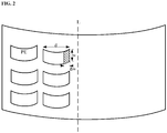
- FIG. 2 is a diagram illustrating the structure of an array substrate.
- the display panel is curved with respect to an axis L.
- the array substrate includes an array of subpixels arranged in rows and columns including a plurality of pixel electrodes PE corresponding to the array of subpixels, each pixel electrode PE in a subpixel.
- the pixel electrode PE has a first dimension d along the row direction and a second dimension w along the column direction.
- the first dimension d in FIG. 2 is a length of a long side of the pixel electrode
- the second dimension w is a width of a short side of the pixel electrode.
- the short side is substantially parallel to the axis L
- the long side is substantially perpendicular to the axis L.
- the first dimension d is larger than the second dimension w.
- each pixel electrode is shifted relative to the counter substrate by a distance ⁇ w.
- each pixel electrode is offset with respect to the counter substrate by an offset region (see the shaded region in FIG. 2 ).
- the offset region has an area of ⁇ w ⁇ w. Because w is much smaller than d, the offset region has an area much smaller than that in the conventional curved display panel. The effects of the offset region on the display quality are minimized, thus the display quality in the present curved display panel is much improved as compared to the conventional curved display panel.
- the black matrix layer is disposed on the counter substrate.
- the offset area between the black matrix layer and the pixel electrode and its effect on aperture ratio of the display apparatus can be minimized.
- the black matrix layer is disposed on the array substrate.
- the pixel electrode has a rectangular shape having a long side along the row direction and a short side along the column direction.
- the short side is substantially parallel to the axis L
- the long side is substantially perpendicular to the axis L.
- the pixel electrode may be made of any appropriate shape, e.g., a parallelogram shape, a trapezoidal shape, an irregular shape, or a shape having protrusions or cut-off portions.
- the pixel electrodes in the present curved display panel are arranged so that a first dimension of the pixel electrode along a row direction is larger than a second dimension of the pixel electrode along a column direction when the curved display panel is curved with respect to an axis substantially parallel to the column direction.
- the first dimension is a maximal dimension of the pixel electrode along the row direction.
- the second dimension is a maximal dimension of the pixel electrode along the column direction.
- each pixel electrode has multiple domains.
- Each domain includes a plurality of branches (e.g., rod-shaped electrodes) extending along a substantially the same direction.
- the plurality of branches in each domain are spaced apart from each other, e.g., adjacent branches are spaced apart from each other by a slit.
- the plurality of branches in each domain are substantially parallel to each other.
- a pattern of a plurality of branches in a domain is axisymmetrical to that in an adjacent domain in a same pixel electrode of a same subpixel.
- the plurality of branches in one domain form an included angle with the plurality of branches in the adjacent domain in the same pixel electrode of the same subpixel.
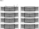
- FIG. 3 is a diagram illustrating the structure of an array substrate according to the present disclosure.
- the array substrate is in a state when the display panel is in a substantially flat state (e.g., not yet curved).
- the black matrix opening 2 is aligned to the center of the pixel electrode 1.
- the position of the black matrix opening 2 also corresponds to the color filter on the counter substrate.
- the plurality of branches of two domains in an area corresponding to the black matrix opening 2 have an axisymmetry with respect to an axis between two domains.
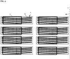
- FIG. 4 is a diagram illustrating the structure of an array substrate according to the present disclosure.
- the array substrate is in a state when the display panel is in a curved with respect to an axis L.
- an offset occurs between the black matrix opening 2 offsets with the pixel electrode 1.
- the plurality of branches of two domains in an area corresponding to the black matrix opening 2 no longer have an axisymmetry, resulting in color shift and a decreased aperture ratio.
- each of the plurality of pixel electrodes has a plurality of domains and has at least a plurality of first branches extending along a first direction and a plurality of second branches extending along a second direction; the first direction being different from the second direction.
- a sum of areas occupied by first branches in a first region of a first subpixel is substantially equal to a sum of area occupied by second branches in a second region of a second subpixel; and a sum of areas occupied by second branches in a first region of a first subpixel is substantially equal to a sum of area occupied by first branches in a second region of a second subpixel; the first subpixel and the second subpixel being two adjacent subpixels along the row direction; and the first region and the second region are two equivalent regions in the first subpixel and the second subpixel, respectively; the first region and the second region are small than a pixel electrode.
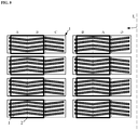
- FIG. 5 is a diagram illustrating the structure of an array substrate according to the present disclosure.
- each pixel electrode includes a first domain A and a second domain B.
- the first domain A includes a plurality of first branches 11 extending along a first direction D1
- the second domain B includes a plurality of second branches 12 extending along a second direction D2; the second direction D2 being different from the first direction D1.
- a first subpixel SP1 on the top left side of the array substrate includes a first domain A on the left and a second domain B on the right
- a second subpixel SP2 adjacent to the first subpixel SP1 along the row direction (on the top right side of the array substrate) includes a second domain B on the left and a first domain A on the right.
- Adjacent domains between the first subpixel SP1 and the second subpixel SP2 extend along difference directions.
- the second domain B in the first subpixel SP1 is adjacent to the second domain B in the second subpixel SP2 along the row direction.
- the first domain A in the first subpixel SP1 is adjacent to the first domain A in the second subpixel SP2 along the row direction.
- the plurality of first branches 11 in the first domain A and the plurality of second branches 12 in the second domain B in a same subpixel have a substantially mirror symmetry with respect to each other.
- the plurality of first branches 11 in the first domain A and the plurality of second branches 12 in the second domain B in a same subpixel have an axisymmetry with respect to an axis located between the first domain A and the second domain B.
- a first pattern including the first domain A and the second domain B in the first subpixel SP1 and a second pattern including the first domain A and the second domain B in the second subpixel SP2 have a substantially two-fold rotational symmetry in plan view of the array of subpixels.
- the first subpixel SP1 has more first branches 11 in an area corresponding to the black matrix opening 2, however, the second subpixel SP2 has more second branches 12 in the area corresponding to the black matrix opening 2. As shown in FIG.
- a sum of areas occupied by first branches 11 in a first region (e.g., a region corresponding to the black matrix opening 2) of a first subpixel SP1 is substantially equal to a sum of area occupied by second branches 12 in a second region (e.g., a region corresponding to the black matrix opening 2) of a second subpixel SP2; and a sum of areas occupied by second branches 12 in a first region of a first subpixel SP1 is substantially equal to a sum of area occupied by first branches 11 in a second region of a second subpixel SP2.
- the first region and the second region may be any equivalent regions in the first subpixel SP1 and the second subpixel SP2, respectively, and are small that a pixel electrode.
- the first region and the second region may be two regions in the first subpixel SP1 and the second subpixel SP2, respectively, that are located at equivalent positions in the first subpixel SP1 and the second subpixel SP2.
- the first region is a region in the first subpixel SP1 corresponding to the black matrix opening 2 in the first subpixel SP1
- the second region is a region in the second subpixel SP2 corresponding to the black matrix opening 2 in the second subpixel SP2.
- a sum of areas occupied by first branches 11 in two equivalent regions in two adjacent subpixels along the row direction is substantially equal to a sum of areas occupied by second branches 12 in the two equivalent regions.
- the first region is a region in the first subpixel SP1 corresponding to the black matrix opening 2 in the first subpixel SP1
- the second region is a region in the second subpixel SP2 corresponding to the black matrix opening 2 in the second subpixel SP2
- the sum of areas occupied by first branches 11 in two adjacent regions along the row direction is X1 + X2
- the sum of areas occupied by second branches 12 in the two adjacent regions is Y1 + Y2.
- a first pattern including the first domain A and the second domain B in the first subpixel SP1 and a second pattern including the first domain A and the second domain B in the second subpixel SP2 have a substantially two-fold rotational symmetry in plan view of the array of subpixels.
- the pixel electrodes in the present array substrate may be made to have various alternative patterns.
- the first pattern and the second pattern may not have a two-fold rotational symmetry, but still the sum of areas occupied by first branches 11 in two equivalent regions in two adjacent subpixels along the row direction is maintained to be substantially equal to the sum of areas occupied by second branches 12 in the two equivalent regions, color shift may be substantially prevented or reduced.
- the array substrate includes one or more vias in the pixel electrodes. Due to the presence of the vias in the pixel electrodes, the first subpixel and the second subpixel along the row direction may not have branch patterns having perfect two-fold rotational symmetry in plan view of the array of subpixels. However, in two adjacent first subpixel and second subpixel along the row direction in such an array substrate, the second domain in the first subpixel is adjacent to the second domain in the second subpixel along the row direction. For example, the first domain in the first subpixel is on a side of the second domain in the first subpixel distal to the second subpixel, and the first domain in the second subpixel is on a side of the second domain in the second subpixel distal to the first subpixel. Referring to FIG.
- the first branches 11 and the second branches 12 in the first subpixel SP1 (top left side of the array of subpixels in FIG. 5 ) form an included angle, the opening of which points upwards.
- the first branches 11 and the second branches 12 in the second subpixel SP2 (top right side of the array of subpixels in FIG. 5 ) form an included angle, the opening of which points downwards.
- the openings of the included angles in the first subpixel SP1 and the second subpixel SP2 are oriented in two opposite directions.
- the offset between the black matrix opening 2 and the pixel electrode 1 is shifted to the left with respect to the center of the pixel electrode.
- the offset between the black matrix opening 2 and the pixel electrode 1 is shifted to the right with respect to the center of the pixel electrode.
- the area occupied by the first branches 11 is larger than the area occupied by the second branches 12.
- the area occupied by the second branches 12 is larger than the area occupied by the first branches 11.
- the pixel electrodes in the array substrate can be arranged so that a sum of areas occupied by first branches in a first region of a first subpixel and a second region of a second subpixel is substantially equal to a sum of area occupied by second branches in the first region of the first subpixel and the second region of the second subpixel.
- the first region and the second region may be any equivalent regions in the first subpixel and the second subpixel, respectively, that are small that a pixel electrode.
- the first region and the second region may be two regions in the first subpixel and the second subpixel, respectively, that are located at equivalent positions in the first subpixel and the second subpixel.
- the first region is a region in the first subpixel corresponding to the black matrix opening in the first subpixel
- the second region is a region in the second subpixel corresponding to the black matrix opening in the second subpixel.
- a sum of areas occupied by first branches in a first region of a first subpixel is substantially equal to a sum of area occupied by second branches in a second region of a second subpixel; a sum of areas occupied by second branches in a first region of a first subpixel is substantially equal to a sum of area occupied by first branches in a second region of a second subpixel; the first subpixel and the second subpixel being two adjacent subpixels along the column direction.
- FIG. 6 is a diagram illustrating the structure of an array substrate according to the present disclosure.
- each pixel electrode includes a first domain A and a second domain B.
- the first domain A includes a plurality of first branches 11 extending along a first direction D1
- the second domain B includes a plurality of second branches 12 extending along a second direction D2; the second direction D2 being different from the first direction D1.
- a first subpixel SP1 includes a first domain A on the left and a second domain B on the right
- a second subpixel SP2 adjacent to the first subpixel SP1 along the column direction includes a second domain B on the left and a first domain A on the right.
- a first pattern including the first domain A and the second domain B in the first subpixel SP1 and a second pattern including the first domain A and the second domain B in the second subpixel SP2 have a substantially mirror symmetry with respect to each other.
- a first pattern including the first domain A and the second domain B in the first subpixel SP1 and a second pattern including the first domain A and the second domain B in the second subpixel SP2 have a substantially two-fold rotational symmetry in plan view of the array of subpixels.
- the array substrate includes one or more vias in the pixel electrodes. Due to the presence of the vias in the pixel electrodes, the first subpixel and the second subpixel along the column direction may not have branch patterns having perfect two-fold rotational symmetry in plan view of the array of subpixels. However, in two adjacent first subpixel and second subpixel along the column direction in such an array substrate, the first domain in the first subpixel is adjacent to the second domain in the second subpixel along the column direction, and the second domain in the first subpixel is adjacent to the first domain in the second subpixel along the column direction.
- the first branches 11 and the second branches 12 in the first subpixel SP1 form an included angle, the opening of which points upwards.
- the first branches 11 and the second branches 12 in the second subpixel SP2 form an included angle, the opening of which points downwards.
- the openings of the included angles in the first subpixel SP1 and the second subpixel SP2 are oriented in two opposite directions.
- each pixel electrode in the present array substrate includes more than two domains.
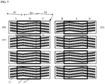
- FIG. 7 is a diagram illustrating the structure of an array substrate according to the present disclosure. Referring to FIG. 7 , each pixel electrode includes three domains.
- the first subpixel SP1 includes a first domain A, a second domain B, and a third domain C.
- the first domain A includes a plurality of first branches 11 extending along a first direction D1
- the second domain B includes a plurality of second branches 12 extending along a second direction D2
- the third domain C includes a plurality of first branches 11 extending along a first direction D1; the second direction D2 being different from the first direction D1.
- the first domain A, the second domain B, and the third domain C are sequentially arranged substantially along the row direction.
- the plurality of first branches 11 in the first domain A and the plurality of second branches 12 in the second domain B in a same subpixel SP1 have mirror symmetry with respect to each other, and the plurality of second branches 12 in the second domain B and the plurality of first branches 11 in the third domain C in the same subpixel SP1 have a substantially mirror symmetry with respect to each other.
- the plurality of first branches 11 in the first domain A and the plurality of second branches 12 in the second domain B in a same subpixel SP1 have an axisymmetry with respect to the axis between the first domain A and the second domain B
- the plurality of second branches 12 in the second domain B and the plurality of first branches 11 in the third domain C in the same subpixel SP1 have an axisymmetry with respect to the axis between the second domain B and the third domain C.
- a second subpixel SP2 adjacent to the first subpixel SP1 includes a second domain B, a first domain A, and a fourth domain D.
- the second domain B includes a plurality of second branches 12 extending along a second direction D2;
- the first domain A includes a plurality of first branches 11 extending along a first direction D1
- the fourth domain D includes a plurality of second branches 12 extending along a second direction D2; the second direction D2 being different from the first direction D1.
- the second domain B, the first domain A, and the fourth domain D are sequentially arranged substantially along the row direction. Branches in adjacent domains between the first subpixel SP1 and the second subpixel SP2 extend along difference directions.
- the third domain C in the first subpixel SP1 is adjacent to the second domain B in the second subpixel SP2 along the row direction.
- the first domain A in the first subpixel SP1 is adjacent to the fourth domain D in the second subpixel SP2 along the row direction.
- a third subpixel SP3 adjacent to the first subpixel SP1 includes a second domain B, a first domain A, and a fourth domain D.
- the second domain B includes a plurality of second branches 12 extending along a second direction D2;
- the first domain A includes a plurality of first branches 11 extending along a first direction D1
- the fourth domain D includes a plurality of second branches 12 extending along a second direction D2; the second direction D2 being different from the first direction D1.
- the second domain B, the first domain A, and the fourth domain D are sequentially arranged substantially along the row direction. Branches in adjacent domains between the first subpixel SP1 and the third subpixel SP3 extend along difference directions.
- the first domain A in the first subpixel SP1 is adjacent to the second domain B in the third subpixel SP3 along the column direction; the second domain B in the first subpixel SP1 is adjacent to the first domain A in the third subpixel SP3 along the column direction; and the third domain C in the first subpixel SP1 is adjacent to the fourth domain D in the third subpixel SP3 along the column direction.
- FIG. 7 the array substrate is in a state in which the display apparatus is in a substantially flat state (e.g., not curved).
- the black matrix opening 2 is aligned with the center of each pixel electrode 1.
- FIG. 8 is a diagram illustrating the structure of an array substrate in some embodiments according to the present disclosure.
- FIG. 8 shown the array substrate in a state in which the display apparatus is curved.
- the black matrix opening 2 is offset with respect to the pixel electrode 1.
- the black matrix opening 2 is substantially aligned with the interface between the first domain A and the second domain B.
- the pattern of first branches 1 and second branches 2 in an area corresponding to the black matrix opening 2 has a substantially mirror symmetry or substantially an axisymmetry with respect to an axis along the interface between the first domain A and the second domain B.
- the size of each domain of the pixel electrode can be determined based on the offset width.
- the array substrate can be designed so that, when the display apparatus is in a curved state, the pattern of branches in an area corresponding to the black matrix opening has a substantially mirror symmetry or substantially an axisymmetry. By having this design, color shift in the display apparatus can be improved.
- the black matrix layer is disposed on the counter substrate.
- the pattern of branches in an area corresponding to the black matrix opening has a substantially mirror symmetry or substantially an axisymmetry.
- the black matrix layer is disposed on the array substrate.
- the pattern of branches in an area corresponding to the color filter block has a substantially mirror symmetry or substantially an axisymmetry.
- the curved display panel further includes a black matrix layer in an inter-subpixel region of the curved display panel.
- the curved display panel further includes a counter substrate facing the array substrate. Furthermore, the black matrix is disposed in the counter substrate.
- the curved display panel further includes a liquid crystal layer between the array substrate and the counter substrate.
- each of the plurality of pixel electrodes includes a first domain having a plurality of first branches extending along the first direction; a second domain having a plurality of second branches extending along the second direction; and a third domain having a plurality of first branches extending along the first direction; the first domain; the second domain, and a third domain being sequentially arranged substantially along the row direction.
- the plurality of first branches in the first domain and the plurality of second branches in the second domain in a same subpixel have a substantially mirror symmetry with respect to each other
- the plurality of second branches in the second domain and the plurality of first branches in the third domain in the same subpixel have a substantially mirror symmetry with respect to each other.
- a projection of the third domain on the curved display panel overlaps with that of the black matrix layer.
- a projection of the first domain and the second domain on the curved display panel is at least partially outside that of the black matrix layer.
- the portion of the first domain and the second domain whose projection is outside that of the black matrix layer has a pattern of first branches and second branches having a substantially mirror symmetry or substantially an axisymmetry.
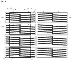
- FIG. 9 illustrates a pixel electrode structure in which each pixel electrode has a plurality of domains A and B, and includes at least a plurality of first branches 11 in domain A extending along a first direction D1 and a plurality of second branches 12 in domain B extending along a second direction D2, the first direction D1 is different from the second direction D2.
- the first branches 11 and the second branches 12 in each pixel electrode offset from each other, thereby destroying any mirror symmetry or axisymmetry.
- a sum of areas occupied by first branches 11 in a first region of a first subpixel SP1 and a second region of a second subpixel SP2 is substantially equal to a sum of area occupied by second branches 12 in the first region of the first subpixel SP1 and the second region of the second subpixel SP2, the first subpixel SP1 and the second subpixel SP2 are two adjacent subpixels along the row direction.
- the first region and the second region are two equivalent regions in the first subpixel SP1 and the second subpixel SP2, respectively; the first region and the second region are small than a pixel electrode.
- the first region and the second region are black matrix opening 2 in the first subpixel SP1 and the second subpixel SP2.
- a first pattern including the first domain A and the second domain B in the first subpixel SP1 and a second pattern including the first domain A and the second domain B in the second subpixel SP2 have a substantially two-fold rotational symmetry in plan view of the array of subpixels.
- a sum of areas occupied by first branches in a first region of a first subpixel SP1 and a third region of a third subpixel SP3 is substantially equal to a sum of area occupied by second branches 12 in the first region of the first subpixel SP1 and the third region of the third subpixel SP3, the first subpixel SP1 and the third subpixel SP3 are two adjacent subpixels along the column direction.
- the first region and the second region are two equivalent regions in the first subpixel SP1 and the third subpixel SP3, respectively; the first region and the third region are small than a pixel electrode.
- the first region and the third region are black matrix opening 2 in the first subpixel SP1 and the third subpixel SP3.
- the present disclosure provides an array substrate in which the black matrix layer and the pixel electrode do not offset with each other along the row direction of the array substrate.
- the black matrix layer is absent in an inter-subpixel region between adjacent subpixels along the row direction, and liquid crystal molecules in the liquid crystal layer in the inter-subpixel region between adjacent subpixels along the row direction have a rotation angle corresponding to a normally black mode.
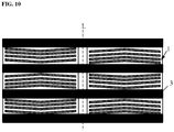
- FIG. 10 is a diagram illustrating the structure of a black matrix layer and an array substrate in a display apparatus according to the present disclosure.
- the curved display panel includes a black matrix layer 3.
- the black matrix layer 3 is disposed in an inter-subpixel region between adjacent subpixels along the column direction, but is absent in the inter-subpixel region between adjacent subpixels along the row direction.
- an offset occurs between the black matrix layer 3 and the array substrate.
- the black matrix layer 3 does not overlap with the pixel electrode 1, and no offset occurs between the black matrix layer 3 and the pixel electrode 1.
- the liquid crystal molecules in the liquid crystal layer in the inter-subpixel region between adjacent subpixels along the row direction have a rotation angle corresponding to a normally black mode.
- the present disclosure provides a curved display apparatus having a curved display panel described herein.
- appropriate curved display apparatuses include, but are not limited to, an electronic paper, a mobile phone, a tablet computer, a television, a monitor, a notebook computer, a digital album, a GPS, etc.
- the curved display apparatus is a liquid crystal display apparatus.
- the curved display apparatus is an organic light emitting display apparatus.
- the term "the invention”, “the present invention” or the like does not necessarily limit the claim scope to a specific embodiment, and the reference to exemplary embodiments of the invention does not imply a limitation on the invention, and no such limitation is to be inferred.
- the invention is limited only by the scope of the appended claims. Moreover, these claims may refer to use "first”, “second”, etc. following with noun or element. Such terms should be understood as a nomenclature and should not be construed as giving the limitation on the number of the elements modified by such nomenclature unless specific number has been given. Any advantages and benefits described may not apply to all embodiments of the invention.
Landscapes
- Physics & Mathematics (AREA)
- Nonlinear Science (AREA)
- Mathematical Physics (AREA)
- Chemical & Material Sciences (AREA)
- Crystallography & Structural Chemistry (AREA)
- General Physics & Mathematics (AREA)
- Optics & Photonics (AREA)
- Geometry (AREA)
- Devices For Indicating Variable Information By Combining Individual Elements (AREA)
- Liquid Crystal (AREA)
Claims (2)
- Gebogene Anzeigetafel mit einem Arraysubstrat, das ein Array von Subpixeln aufweist, die in Zeilen und Spalten angeordnet sind, wobei das Arraysubstrat aufweist:mehrere Pixelelektroden, die dem Array von Subpixeln entsprechen; wobei jede der mehreren Pixelelektroden sich in einem entsprechenden Subpixel befindet und eine erste Abmessung entlang einer Zeilenrichtung und eine zweite Abmessung entlang einer Spaltenrichtung hat;wobei die gebogene Anzeigetafel entlang der Zeilenrichtung in Bezug auf eine Achse, die im Wesentlichen parallel zu der Spaltenrichtung ist, gebogen ist; unddie erste Abmessung größer als die zweite Abmessung ist,wobei die gebogene Anzeigetafel ferner eine schwarze Matrixschicht in einem Zwischen-Subpixelbereich der gebogenen Anzeigetafel, wobei die schwarze Matrix Öffnungen (2) hat, die den Subpixeln entsprechen, und ein Gegensubstrat, das dem Arraysubstrat zugewandt ist, aufweist; wobei sich die schwarze Matrixschicht auf dem Gegensubstrat befindet, undjede der mehreren Pixelelektroden eine erste Domäne (A), die mehrere erste Zweige (11) aufweist, die sich entlang einer ersten Richtung erstrecken; eine zweite Domäne (B), die mehrere zweite Zweige (12) aufweist, die sich entlang einer zweiten Richtung erstrecken, wobei sich die zweite Richtung von der ersten Richtung unterscheidet; und eine dritte Domäne (C), die mehrere ersten Zweige (11) aufweist, die sich entlang der ersten Richtung erstrecken, umfasst; wobei die erste Domäne (A); die zweite Domäne (B) und die dritte Domäne (C) im Wesentlichen entlang der Zeilenrichtung in dieser Reihenfolge aufeinanderfolgend angeordnet sind;die mehreren ersten Zweige (11) in der ersten Domäne (A) und die mehreren zweiten Zweige (12) in der zweiten Domäne (B) in einem gleichen Subpixel zueinander im Wesentlichen spiegelsymmetrisch sind;die mehreren zweiten Zweige (12) in der zweiten Domäne (B) und die mehreren ersten Zweige (11) in der dritten Domäne (C) in dem gleichen Subpixel zueinander im Wesentlichen spiegelsymmetrisch sind;wobei die schwarze Matrixöffnung, die einem Subpixel entspricht, in Bezug auf sein entsprechendes Subpixel versetzt ist, so dass die Projektion der dritten Domäne (C) auf dem Arraysubstrat mit derjenigen der schwarzen Matrixschicht bedeckt ist; unddie Projektion der ersten Domäne (A) und der zweiten Domäne (B) auf dem Arraysubstrat zumindest teilweise nicht mit derjenigen der schwarzen Matrixschicht bedeckt ist.
- Gebogene Anzeigevorrichtung, eine gebogene Anzeigetafel nach Anspruch 1 aufweisend.
Applications Claiming Priority (2)
| Application Number | Priority Date | Filing Date | Title |
|---|---|---|---|
| CN201510824572.6A CN105259716B (zh) | 2015-11-24 | 2015-11-24 | 一种阵列基板、曲面显示面板及曲面显示装置 |
| PCT/CN2016/104916 WO2017088636A1 (en) | 2015-11-24 | 2016-11-07 | Curved display panel and curved display apparatus |
Publications (3)
| Publication Number | Publication Date |
|---|---|
| EP3380889A1 EP3380889A1 (de) | 2018-10-03 |
| EP3380889A4 EP3380889A4 (de) | 2019-04-24 |
| EP3380889B1 true EP3380889B1 (de) | 2021-04-07 |
Family
ID=55099466
Family Applications (1)
| Application Number | Title | Priority Date | Filing Date |
|---|---|---|---|
| EP16852870.1A Active EP3380889B1 (de) | 2015-11-24 | 2016-11-07 | Gebogene anzeigetafel und gebogene anzeigevorrichtung |
Country Status (4)
| Country | Link |
|---|---|
| US (1) | US10678102B2 (de) |
| EP (1) | EP3380889B1 (de) |
| CN (1) | CN105259716B (de) |
| WO (1) | WO2017088636A1 (de) |
Families Citing this family (10)
| Publication number | Priority date | Publication date | Assignee | Title |
|---|---|---|---|---|
| CN105259716B (zh) * | 2015-11-24 | 2018-08-03 | 京东方科技集团股份有限公司 | 一种阵列基板、曲面显示面板及曲面显示装置 |
| TW201734605A (zh) * | 2016-03-18 | 2017-10-01 | 友達光電股份有限公司 | 陣列基板以及曲面液晶顯示面板 |
| CN105789264A (zh) | 2016-05-06 | 2016-07-20 | 京东方科技集团股份有限公司 | 一种曲面显示面板及其制备方法、显示装置 |
| CN105929616B (zh) * | 2016-07-06 | 2020-03-10 | 深圳市华星光电技术有限公司 | 异形显示屏及其像素单元结构 |
| JP6921509B2 (ja) * | 2016-11-30 | 2021-08-18 | 株式会社ジャパンディスプレイ | 液晶表示装置 |
| TWI589972B (zh) * | 2016-12-28 | 2017-07-01 | 友達光電股份有限公司 | 主動元件陣列基板及應用其之液晶面板 |
| CN107067984A (zh) * | 2017-06-09 | 2017-08-18 | 京东方科技集团股份有限公司 | 曲面显示面板的制作方法、曲面显示面板及曲面显示装置 |
| KR102436563B1 (ko) * | 2017-12-27 | 2022-08-26 | 엘지디스플레이 주식회사 | 표시장치 |
| CN108563079B (zh) * | 2018-03-22 | 2021-07-09 | 厦门天马微电子有限公司 | 曲面显示面板及显示装置 |
| CN111668241B (zh) * | 2020-06-30 | 2023-07-18 | 京东方科技集团股份有限公司 | 有机发光显示面板、显示装置 |
Family Cites Families (20)
| Publication number | Priority date | Publication date | Assignee | Title |
|---|---|---|---|---|
| JP2003322867A (ja) * | 2002-05-08 | 2003-11-14 | Hitachi Ltd | アクティブマトリクス型液晶表示装置 |
| JP4049639B2 (ja) * | 2002-08-30 | 2008-02-20 | シャープ株式会社 | 液晶表示装置用基板及びそれを備えた液晶表示装置 |
| CN100495180C (zh) * | 2006-09-07 | 2009-06-03 | 瀚宇彩晶股份有限公司 | 液晶显示器装置 |
| CN100545725C (zh) | 2006-12-28 | 2009-09-30 | 中华映管股份有限公司 | 像素结构与液晶显示面板 |
| CN101290410B (zh) | 2007-04-17 | 2011-06-15 | 北京京东方光电科技有限公司 | 液晶面板阵列结构 |
| JP5322427B2 (ja) * | 2007-12-19 | 2013-10-23 | 三菱電機株式会社 | 液晶表示装置 |
| KR101644525B1 (ko) * | 2009-07-20 | 2016-08-02 | 삼성디스플레이 주식회사 | 표시 기판 및 이를 갖는 표시 장치 |
| TWI471670B (zh) * | 2010-09-29 | 2015-02-01 | Au Optronics Corp | 液晶顯示面板 |
| TW201241529A (en) * | 2011-04-11 | 2012-10-16 | Hannstar Display Corp | Liquid crystal display panel |
| CN102768445B (zh) | 2012-07-18 | 2015-04-22 | 深圳市华星光电技术有限公司 | 子像素显示结构及其应用的液晶显示面板 |
| KR20140141364A (ko) * | 2013-05-31 | 2014-12-10 | 삼성디스플레이 주식회사 | 표시 장치 및 그 제조 방법 |
| KR20150068156A (ko) | 2013-12-11 | 2015-06-19 | 삼성디스플레이 주식회사 | 액정 표시 장치 |
| TWI542932B (zh) * | 2014-07-22 | 2016-07-21 | 友達光電股份有限公司 | 顯示面板及曲面顯示器 |
| KR20160045186A (ko) * | 2014-10-16 | 2016-04-27 | 삼성디스플레이 주식회사 | 표시 장치 |
| CN104375339B (zh) | 2014-11-13 | 2017-07-18 | 深圳市华星光电技术有限公司 | 曲面液晶显示面板及曲面液晶显示装置 |
| CN104503156A (zh) * | 2014-12-11 | 2015-04-08 | 深圳市华星光电技术有限公司 | 显示基板及其制造方法 |
| KR102289275B1 (ko) * | 2015-01-09 | 2021-08-12 | 삼성디스플레이 주식회사 | 액정 표시 장치 |
| TWI561890B (en) * | 2015-08-10 | 2016-12-11 | Au Optronics Corp | Pixel array, display panel and curved display panel |
| CN205121121U (zh) * | 2015-11-24 | 2016-03-30 | 京东方科技集团股份有限公司 | 一种显示面板及显示装置 |
| CN105259716B (zh) * | 2015-11-24 | 2018-08-03 | 京东方科技集团股份有限公司 | 一种阵列基板、曲面显示面板及曲面显示装置 |
-
2015
- 2015-11-24 CN CN201510824572.6A patent/CN105259716B/zh active Active
-
2016
- 2016-11-07 EP EP16852870.1A patent/EP3380889B1/de active Active
- 2016-11-07 WO PCT/CN2016/104916 patent/WO2017088636A1/en not_active Ceased
- 2016-11-07 US US15/519,621 patent/US10678102B2/en active Active
Non-Patent Citations (1)
| Title |
|---|
| None * |
Also Published As
| Publication number | Publication date |
|---|---|
| CN105259716A (zh) | 2016-01-20 |
| EP3380889A1 (de) | 2018-10-03 |
| CN105259716B (zh) | 2018-08-03 |
| US20170357132A1 (en) | 2017-12-14 |
| US10678102B2 (en) | 2020-06-09 |
| EP3380889A4 (de) | 2019-04-24 |
| WO2017088636A1 (en) | 2017-06-01 |
Similar Documents
| Publication | Publication Date | Title |
|---|---|---|
| EP3380889B1 (de) | Gebogene anzeigetafel und gebogene anzeigevorrichtung | |
| US9858870B2 (en) | Pixel unit, pixel array and liquid crystal display panel | |
| US10459302B2 (en) | Array substrate, display panel and display device | |
| EP3453051B1 (de) | Gekrümmte anzeigetafel, gekrümmte anzeigevorrichtung und herstellungsverfahren dafür | |
| TWI551921B (zh) | 顯示面板 | |
| TWI464491B (zh) | 顯示裝置 | |
| US9846327B2 (en) | Liquid crystal display with reduced color mixing | |
| TWI581043B (zh) | 畫素結構 | |
| US10203569B2 (en) | Array substrate and display panel | |
| WO2016201928A1 (en) | Array substrate, display panel and display device having the same, and method thereof | |
| WO2019041910A1 (zh) | 显示面板以及显示装置 | |
| US20140111749A1 (en) | Transparent display panel and transparent display apparatus having the same | |
| US20130271683A1 (en) | Display apparatus | |
| KR20150086829A (ko) | 액정 표시 장치 | |
| JP6374144B2 (ja) | 液晶表示装置 | |
| EP2562592A1 (de) | Flüssigkristallanzeigevorrichtung | |
| US7978271B2 (en) | Multi-domain liquid crystal display and array substrate thereof comprising a storage capacitor having an auxiliary electrode controlled by a preceding scan line or signal line | |
| WO2016138721A1 (zh) | 液晶屏及显示装置 | |
| TW201911433A (zh) | 畫素結構 | |
| CN110543039B (zh) | 显示面板和显示装置 | |
| US9442329B2 (en) | Liquid crystal display | |
| US11294250B2 (en) | Display device | |
| US10444573B2 (en) | Liquid crystal array substrate, liquid crystal display panel, and liquid crystal display apparatus | |
| US20160004134A1 (en) | Array substrate, method for fabricating the same and display device | |
| JP2007058155A (ja) | マルチドメイン垂直配向液晶表示パネル、薄膜トランジスタアレイ、およびその製造方法 |
Legal Events
| Date | Code | Title | Description |
|---|---|---|---|
| STAA | Information on the status of an ep patent application or granted ep patent |
Free format text: STATUS: UNKNOWN |
|
| STAA | Information on the status of an ep patent application or granted ep patent |
Free format text: STATUS: THE INTERNATIONAL PUBLICATION HAS BEEN MADE |
|
| PUAI | Public reference made under article 153(3) epc to a published international application that has entered the european phase |
Free format text: ORIGINAL CODE: 0009012 |
|
| STAA | Information on the status of an ep patent application or granted ep patent |
Free format text: STATUS: REQUEST FOR EXAMINATION WAS MADE |
|
| 17P | Request for examination filed |
Effective date: 20170412 |
|
| AK | Designated contracting states |
Kind code of ref document: A1 Designated state(s): AL AT BE BG CH CY CZ DE DK EE ES FI FR GB GR HR HU IE IS IT LI LT LU LV MC MK MT NL NO PL PT RO RS SE SI SK SM TR |
|
| AX | Request for extension of the european patent |
Extension state: BA ME |
|
| DAV | Request for validation of the european patent (deleted) | ||
| DAX | Request for extension of the european patent (deleted) | ||
| A4 | Supplementary search report drawn up and despatched |
Effective date: 20190327 |
|
| RIC1 | Information provided on ipc code assigned before grant |
Ipc: G02F 1/1335 20060101ALI20190321BHEP Ipc: G02F 1/1343 20060101AFI20190321BHEP |
|
| STAA | Information on the status of an ep patent application or granted ep patent |
Free format text: STATUS: EXAMINATION IS IN PROGRESS |
|
| 17Q | First examination report despatched |
Effective date: 20200128 |
|
| GRAP | Despatch of communication of intention to grant a patent |
Free format text: ORIGINAL CODE: EPIDOSNIGR1 |
|
| STAA | Information on the status of an ep patent application or granted ep patent |
Free format text: STATUS: GRANT OF PATENT IS INTENDED |
|
| INTG | Intention to grant announced |
Effective date: 20201023 |
|
| GRAS | Grant fee paid |
Free format text: ORIGINAL CODE: EPIDOSNIGR3 |
|
| GRAA | (expected) grant |
Free format text: ORIGINAL CODE: 0009210 |
|
| STAA | Information on the status of an ep patent application or granted ep patent |
Free format text: STATUS: THE PATENT HAS BEEN GRANTED |
|
| AK | Designated contracting states |
Kind code of ref document: B1 Designated state(s): AL AT BE BG CH CY CZ DE DK EE ES FI FR GB GR HR HU IE IS IT LI LT LU LV MC MK MT NL NO PL PT RO RS SE SI SK SM TR |
|
| REG | Reference to a national code |
Ref country code: GB Ref legal event code: FG4D |
|
| REG | Reference to a national code |
Ref country code: AT Ref legal event code: REF Ref document number: 1380460 Country of ref document: AT Kind code of ref document: T Effective date: 20210415 Ref country code: CH Ref legal event code: EP |
|
| REG | Reference to a national code |
Ref country code: DE Ref legal event code: R096 Ref document number: 602016055833 Country of ref document: DE |
|
| REG | Reference to a national code |
Ref country code: IE Ref legal event code: FG4D |
|
| REG | Reference to a national code |
Ref country code: LT Ref legal event code: MG9D |
|
| REG | Reference to a national code |
Ref country code: NL Ref legal event code: MP Effective date: 20210407 Ref country code: AT Ref legal event code: MK05 Ref document number: 1380460 Country of ref document: AT Kind code of ref document: T Effective date: 20210407 |
|
| PG25 | Lapsed in a contracting state [announced via postgrant information from national office to epo] |
Ref country code: FI Free format text: LAPSE BECAUSE OF FAILURE TO SUBMIT A TRANSLATION OF THE DESCRIPTION OR TO PAY THE FEE WITHIN THE PRESCRIBED TIME-LIMIT Effective date: 20210407 Ref country code: LT Free format text: LAPSE BECAUSE OF FAILURE TO SUBMIT A TRANSLATION OF THE DESCRIPTION OR TO PAY THE FEE WITHIN THE PRESCRIBED TIME-LIMIT Effective date: 20210407 Ref country code: HR Free format text: LAPSE BECAUSE OF FAILURE TO SUBMIT A TRANSLATION OF THE DESCRIPTION OR TO PAY THE FEE WITHIN THE PRESCRIBED TIME-LIMIT Effective date: 20210407 Ref country code: BG Free format text: LAPSE BECAUSE OF FAILURE TO SUBMIT A TRANSLATION OF THE DESCRIPTION OR TO PAY THE FEE WITHIN THE PRESCRIBED TIME-LIMIT Effective date: 20210707 Ref country code: AT Free format text: LAPSE BECAUSE OF FAILURE TO SUBMIT A TRANSLATION OF THE DESCRIPTION OR TO PAY THE FEE WITHIN THE PRESCRIBED TIME-LIMIT Effective date: 20210407 Ref country code: NL Free format text: LAPSE BECAUSE OF FAILURE TO SUBMIT A TRANSLATION OF THE DESCRIPTION OR TO PAY THE FEE WITHIN THE PRESCRIBED TIME-LIMIT Effective date: 20210407 |
|
| PG25 | Lapsed in a contracting state [announced via postgrant information from national office to epo] |
Ref country code: SE Free format text: LAPSE BECAUSE OF FAILURE TO SUBMIT A TRANSLATION OF THE DESCRIPTION OR TO PAY THE FEE WITHIN THE PRESCRIBED TIME-LIMIT Effective date: 20210407 Ref country code: RS Free format text: LAPSE BECAUSE OF FAILURE TO SUBMIT A TRANSLATION OF THE DESCRIPTION OR TO PAY THE FEE WITHIN THE PRESCRIBED TIME-LIMIT Effective date: 20210407 Ref country code: PT Free format text: LAPSE BECAUSE OF FAILURE TO SUBMIT A TRANSLATION OF THE DESCRIPTION OR TO PAY THE FEE WITHIN THE PRESCRIBED TIME-LIMIT Effective date: 20210809 Ref country code: NO Free format text: LAPSE BECAUSE OF FAILURE TO SUBMIT A TRANSLATION OF THE DESCRIPTION OR TO PAY THE FEE WITHIN THE PRESCRIBED TIME-LIMIT Effective date: 20210707 Ref country code: PL Free format text: LAPSE BECAUSE OF FAILURE TO SUBMIT A TRANSLATION OF THE DESCRIPTION OR TO PAY THE FEE WITHIN THE PRESCRIBED TIME-LIMIT Effective date: 20210407 Ref country code: LV Free format text: LAPSE BECAUSE OF FAILURE TO SUBMIT A TRANSLATION OF THE DESCRIPTION OR TO PAY THE FEE WITHIN THE PRESCRIBED TIME-LIMIT Effective date: 20210407 Ref country code: GR Free format text: LAPSE BECAUSE OF FAILURE TO SUBMIT A TRANSLATION OF THE DESCRIPTION OR TO PAY THE FEE WITHIN THE PRESCRIBED TIME-LIMIT Effective date: 20210708 Ref country code: IS Free format text: LAPSE BECAUSE OF FAILURE TO SUBMIT A TRANSLATION OF THE DESCRIPTION OR TO PAY THE FEE WITHIN THE PRESCRIBED TIME-LIMIT Effective date: 20210807 |
|
| REG | Reference to a national code |
Ref country code: DE Ref legal event code: R097 Ref document number: 602016055833 Country of ref document: DE |
|
| PG25 | Lapsed in a contracting state [announced via postgrant information from national office to epo] |
Ref country code: RO Free format text: LAPSE BECAUSE OF FAILURE TO SUBMIT A TRANSLATION OF THE DESCRIPTION OR TO PAY THE FEE WITHIN THE PRESCRIBED TIME-LIMIT Effective date: 20210407 Ref country code: ES Free format text: LAPSE BECAUSE OF FAILURE TO SUBMIT A TRANSLATION OF THE DESCRIPTION OR TO PAY THE FEE WITHIN THE PRESCRIBED TIME-LIMIT Effective date: 20210407 Ref country code: DK Free format text: LAPSE BECAUSE OF FAILURE TO SUBMIT A TRANSLATION OF THE DESCRIPTION OR TO PAY THE FEE WITHIN THE PRESCRIBED TIME-LIMIT Effective date: 20210407 Ref country code: EE Free format text: LAPSE BECAUSE OF FAILURE TO SUBMIT A TRANSLATION OF THE DESCRIPTION OR TO PAY THE FEE WITHIN THE PRESCRIBED TIME-LIMIT Effective date: 20210407 Ref country code: CZ Free format text: LAPSE BECAUSE OF FAILURE TO SUBMIT A TRANSLATION OF THE DESCRIPTION OR TO PAY THE FEE WITHIN THE PRESCRIBED TIME-LIMIT Effective date: 20210407 Ref country code: SK Free format text: LAPSE BECAUSE OF FAILURE TO SUBMIT A TRANSLATION OF THE DESCRIPTION OR TO PAY THE FEE WITHIN THE PRESCRIBED TIME-LIMIT Effective date: 20210407 Ref country code: SM Free format text: LAPSE BECAUSE OF FAILURE TO SUBMIT A TRANSLATION OF THE DESCRIPTION OR TO PAY THE FEE WITHIN THE PRESCRIBED TIME-LIMIT Effective date: 20210407 |
|
| PLBE | No opposition filed within time limit |
Free format text: ORIGINAL CODE: 0009261 |
|
| STAA | Information on the status of an ep patent application or granted ep patent |
Free format text: STATUS: NO OPPOSITION FILED WITHIN TIME LIMIT |
|
| 26N | No opposition filed |
Effective date: 20220110 |
|
| PG25 | Lapsed in a contracting state [announced via postgrant information from national office to epo] |
Ref country code: IS Free format text: LAPSE BECAUSE OF FAILURE TO SUBMIT A TRANSLATION OF THE DESCRIPTION OR TO PAY THE FEE WITHIN THE PRESCRIBED TIME-LIMIT Effective date: 20210807 Ref country code: AL Free format text: LAPSE BECAUSE OF FAILURE TO SUBMIT A TRANSLATION OF THE DESCRIPTION OR TO PAY THE FEE WITHIN THE PRESCRIBED TIME-LIMIT Effective date: 20210407 |
|
| PG25 | Lapsed in a contracting state [announced via postgrant information from national office to epo] |
Ref country code: MC Free format text: LAPSE BECAUSE OF FAILURE TO SUBMIT A TRANSLATION OF THE DESCRIPTION OR TO PAY THE FEE WITHIN THE PRESCRIBED TIME-LIMIT Effective date: 20210407 |
|
| REG | Reference to a national code |
Ref country code: CH Ref legal event code: PL |
|
| PG25 | Lapsed in a contracting state [announced via postgrant information from national office to epo] |
Ref country code: LU Free format text: LAPSE BECAUSE OF NON-PAYMENT OF DUE FEES Effective date: 20211107 Ref country code: IT Free format text: LAPSE BECAUSE OF FAILURE TO SUBMIT A TRANSLATION OF THE DESCRIPTION OR TO PAY THE FEE WITHIN THE PRESCRIBED TIME-LIMIT Effective date: 20210407 Ref country code: BE Free format text: LAPSE BECAUSE OF NON-PAYMENT OF DUE FEES Effective date: 20211130 |
|
| REG | Reference to a national code |
Ref country code: BE Ref legal event code: MM Effective date: 20211130 |
|
| PG25 | Lapsed in a contracting state [announced via postgrant information from national office to epo] |
Ref country code: IE Free format text: LAPSE BECAUSE OF NON-PAYMENT OF DUE FEES Effective date: 20211107 |
|
| PG25 | Lapsed in a contracting state [announced via postgrant information from national office to epo] |
Ref country code: FR Free format text: LAPSE BECAUSE OF NON-PAYMENT OF DUE FEES Effective date: 20211130 |
|
| PG25 | Lapsed in a contracting state [announced via postgrant information from national office to epo] |
Ref country code: HU Free format text: LAPSE BECAUSE OF FAILURE TO SUBMIT A TRANSLATION OF THE DESCRIPTION OR TO PAY THE FEE WITHIN THE PRESCRIBED TIME-LIMIT; INVALID AB INITIO Effective date: 20161107 |
|
| PG25 | Lapsed in a contracting state [announced via postgrant information from national office to epo] |
Ref country code: CY Free format text: LAPSE BECAUSE OF FAILURE TO SUBMIT A TRANSLATION OF THE DESCRIPTION OR TO PAY THE FEE WITHIN THE PRESCRIBED TIME-LIMIT Effective date: 20210407 |
|
| PG25 | Lapsed in a contracting state [announced via postgrant information from national office to epo] |
Ref country code: LI Free format text: LAPSE BECAUSE OF NON-PAYMENT OF DUE FEES Effective date: 20220630 Ref country code: CH Free format text: LAPSE BECAUSE OF NON-PAYMENT OF DUE FEES Effective date: 20220630 |
|
| PG25 | Lapsed in a contracting state [announced via postgrant information from national office to epo] |
Ref country code: MK Free format text: LAPSE BECAUSE OF FAILURE TO SUBMIT A TRANSLATION OF THE DESCRIPTION OR TO PAY THE FEE WITHIN THE PRESCRIBED TIME-LIMIT Effective date: 20210407 |
|
| PG25 | Lapsed in a contracting state [announced via postgrant information from national office to epo] |
Ref country code: MT Free format text: LAPSE BECAUSE OF FAILURE TO SUBMIT A TRANSLATION OF THE DESCRIPTION OR TO PAY THE FEE WITHIN THE PRESCRIBED TIME-LIMIT Effective date: 20210407 |
|
| PG25 | Lapsed in a contracting state [announced via postgrant information from national office to epo] |
Ref country code: TR Free format text: LAPSE BECAUSE OF FAILURE TO SUBMIT A TRANSLATION OF THE DESCRIPTION OR TO PAY THE FEE WITHIN THE PRESCRIBED TIME-LIMIT Effective date: 20210407 |
|
| PGFP | Annual fee paid to national office [announced via postgrant information from national office to epo] |
Ref country code: DE Payment date: 20251121 Year of fee payment: 10 |
|
| PGFP | Annual fee paid to national office [announced via postgrant information from national office to epo] |
Ref country code: GB Payment date: 20251121 Year of fee payment: 10 |