EP3382893B1 - Râtelier comprenant un amplificateur hf de haute puissance - Google Patents
Râtelier comprenant un amplificateur hf de haute puissance Download PDFInfo
- Publication number
- EP3382893B1 EP3382893B1 EP17163058.5A EP17163058A EP3382893B1 EP 3382893 B1 EP3382893 B1 EP 3382893B1 EP 17163058 A EP17163058 A EP 17163058A EP 3382893 B1 EP3382893 B1 EP 3382893B1
- Authority
- EP
- European Patent Office
- Prior art keywords
- rack
- power
- combiner
- vertical posts
- power combiner
- Prior art date
- Legal status (The legal status is an assumption and is not a legal conclusion. Google has not performed a legal analysis and makes no representation as to the accuracy of the status listed.)
- Active
Links
Images




Classifications
-
- H—ELECTRICITY
- H05—ELECTRIC TECHNIQUES NOT OTHERWISE PROVIDED FOR
- H05K—PRINTED CIRCUITS; CASINGS OR CONSTRUCTIONAL DETAILS OF ELECTRIC APPARATUS; MANUFACTURE OF ASSEMBLAGES OF ELECTRICAL COMPONENTS
- H05K7/00—Constructional details common to different types of electric apparatus
- H05K7/18—Construction of rack or frame
-
- H—ELECTRICITY
- H03—ELECTRONIC CIRCUITRY
- H03F—AMPLIFIERS
- H03F1/00—Details of amplifiers with only discharge tubes, only semiconductor devices or only unspecified devices as amplifying elements
-
- H—ELECTRICITY
- H03—ELECTRONIC CIRCUITRY
- H03F—AMPLIFIERS
- H03F3/00—Amplifiers with only discharge tubes or only semiconductor devices as amplifying elements
- H03F3/20—Power amplifiers, e.g. Class B amplifiers, Class C amplifiers
- H03F3/21—Power amplifiers, e.g. Class B amplifiers, Class C amplifiers with semiconductor devices only
- H03F3/211—Power amplifiers, e.g. Class B amplifiers, Class C amplifiers with semiconductor devices only using a combination of several amplifiers
-
- H—ELECTRICITY
- H03—ELECTRONIC CIRCUITRY
- H03F—AMPLIFIERS
- H03F3/00—Amplifiers with only discharge tubes or only semiconductor devices as amplifying elements
- H03F3/189—High-frequency amplifiers, e.g. radio frequency amplifiers
-
- H—ELECTRICITY
- H03—ELECTRONIC CIRCUITRY
- H03F—AMPLIFIERS
- H03F3/00—Amplifiers with only discharge tubes or only semiconductor devices as amplifying elements
- H03F3/60—Amplifiers in which coupling networks have distributed constants, e.g. with waveguide resonators
- H03F3/602—Combinations of several amplifiers
-
- H—ELECTRICITY
- H05—ELECTRIC TECHNIQUES NOT OTHERWISE PROVIDED FOR
- H05K—PRINTED CIRCUITS; CASINGS OR CONSTRUCTIONAL DETAILS OF ELECTRIC APPARATUS; MANUFACTURE OF ASSEMBLAGES OF ELECTRICAL COMPONENTS
- H05K7/00—Constructional details common to different types of electric apparatus
- H05K7/14—Mounting supporting structure in casing or on frame or rack
- H05K7/1422—Printed circuit boards receptacles, e.g. stacked structures, electronic circuit modules or box like frames
- H05K7/1424—Card cages
-
- H—ELECTRICITY
- H05—ELECTRIC TECHNIQUES NOT OTHERWISE PROVIDED FOR
- H05K—PRINTED CIRCUITS; CASINGS OR CONSTRUCTIONAL DETAILS OF ELECTRIC APPARATUS; MANUFACTURE OF ASSEMBLAGES OF ELECTRICAL COMPONENTS
- H05K7/00—Constructional details common to different types of electric apparatus
- H05K7/20—Modifications to facilitate cooling, ventilating, or heating
- H05K7/20536—Modifications to facilitate cooling, ventilating, or heating for racks or cabinets of standardised dimensions, e.g. electronic racks for aircraft or telecommunication equipment
- H05K7/207—Thermal management, e.g. cabinet temperature control
-
- H—ELECTRICITY
- H03—ELECTRONIC CIRCUITRY
- H03F—AMPLIFIERS
- H03F2203/00—Indexing scheme relating to amplifiers with only discharge tubes or only semiconductor devices as amplifying elements covered by H03F3/00
- H03F2203/20—Indexing scheme relating to power amplifiers, e.g. Class B amplifiers, Class C amplifiers
- H03F2203/21—Indexing scheme relating to power amplifiers, e.g. Class B amplifiers, Class C amplifiers with semiconductor devices only
- H03F2203/211—Indexing scheme relating to power amplifiers, e.g. Class B amplifiers, Class C amplifiers with semiconductor devices only using a combination of several amplifiers
- H03F2203/21142—Output signals of a plurality of power amplifiers are parallel combined to a common output
Definitions
- the invention relates to a rack comprising a high power RF amplifier, more specifically to a rack comprising a plurality of interconnected RF amplifier modules whose outputs are combined to deliver a high power RF output.
- Radio-Frequency (RF) power amplifiers make more and more use of solid state devices (SSD) such as power semiconductors instead of electronic vacuum tubes (triodes, tetrodes, ...) for amplifying RF signals to high powers.
- SSD solid state devices
- Known SSDs are however not capable of delivering power levels of tens or even hundreds of kilowatts, which are for example required to generate accelerating electric fields in particle accelerators. It is therefore known to combine outputs of multiple SSD amplifier modules to achieve the desired high power output. It is further known to mount SSD amplifier modules in racks and to combine their respective outputs to achieve the desired high power output.
- Patent publication number US2011/149526 discloses a rack comprising SSD amplifier modules and power combiners. The power combiners occupy a certain volume at a back side of the rack which can therefore not be used for SSD amplifier modules and/or for other equipment.
- Patent publication number WO2015023203A1 discloses a power combiner which is adapted to be mounted in a 19 inch rack. Such a power combiner occupies useful volume in the rack, which cannot be used for SSD amplifier modules and/or for other equipment.
- this combiner with two times six horizontally aligned power inputs makes it furthermore necessary to use a plurality of cable connections to the power outputs of the SSD amplifier modules, so that when one wants to remove one SSD amplifier module from the rack, it is most likely that such cable connections to other SSD amplifier modules must first be dismantled, which is inconvenient.
- a rack for mounting multiple equipment modules said rack presenting a left side, a right side a front side, a back side, a top side and a bottom side.
- Said rack comprises a frame having left-side vertical posts and right-side vertical posts, and a plurality of RF amplifier modules, mounted to the frame between the left-side vertical posts on the one hand and the right-side vertical posts on the other hand, each amplifier module comprising an RF amplifier circuit having an RF input and an amplified RF output.
- the rack further comprises a first RF power combiner having first combiner inputs which are connected respectively to the amplified RF outputs of the plurality of RF amplifier modules to deliver a first combined RF power output.
- the first RF power combiner is mounted in the rack, at least partially in a volume comprised between the left-side vertical posts of the frame or at least partially in a volume comprised between the right-side vertical posts of the frame.
- Each RF amplifier module has a front face located at the front side of the rack, and said front face comprises an electrical circuit linking the amplified RF output of the RF amplifier module to the first RF power combiner. Thanks to this arrangement, volume which is conventionally not used for placing equipment in a rack, is now used for placing at least a part of the first RF power combiner. Hence, compared to conventional arrangements, the overall system will occupy less volume and/or present less footprint.
- the front face has both a mechanical and an electrical function, which saves cost and volume.
- each RF amplifier module is removably mounted in the rack, and its front face comprises a first connector to removably connect the electrical circuit to the first RF power combiner, said first connector being arranged at a distal left side and/or at a distal right side of the said front face.
- This facilitates the removal and re-insertion of an RF amplifier module into the rack, without having to use loose cables or other components to link each RF amplifier module to the first power combiner.
- This also provides for a more accurate connection between an RF amplifier module and the first RF power combiner, because an operator can better see the said connection while it is being established.
- each RF amplifier module comprises a printed circuit board with an RF amplifier circuit, its front face is removably mounted to the printed circuit board, and the electrical circuit of its front face is connected to the amplified RF output of said RF amplifier module via a second connector. This allows to an RF amplifier module without the presence of the electrical circuit of its front face.
- the first RF power combiner is completely contained in the volume comprised between the left-side vertical posts of the frame or completely contained in the volume comprised between the right-side vertical posts of the frame.
- the first RF power combiner is partially contained in the volume comprised between the left-side vertical posts of the frame and/or partially contained in the volume comprised between the right-side vertical posts of the frame, and the remaining part of the first RF power combiner is at least partially arranged on the front face of each RF amplifier module.
- the first RF power combiner is a Gysel type combiner (see " A new N-way power divider/combiner suitable for High power applications” - Ulrich H. Gysel - Stanford Research Institute - Menlo Park, California 94025 ),.
- a nominal frequency range of each RF amplifier module is comprised in the range of 3 MHz to 3 GHz. More preferably, the nominal frequency range of each RF amplifier module is comprised in the range of 10 MHz to 300 MHz.
- a nominal output power of each RF amplifier module is comprised in the range of 1 KW to 100 KW. More preferably, a nominal output power of each RF amplifier module is comprised in the range of 3 KW to 30 KW.
- Fig.1 shows an exemplary embodiment of a rack (1) according to the invention.
- the rack (1) has an overall parallelepiped shape and presents a left side (2), a right side (3) a front side (4), a back side (5), a top side and a bottom side.
- the rack (1) comprises a frame having two (extreme) left-side vertical posts (7) and two (extreme) right-side vertical posts (8), and a plurality of RF amplifier modules (10).
- Each RF amplifier module (10) is mounted to the frame between the two left-side vertical posts (7) on the one hand and the two right-side vertical posts (8) on the other hand.
- the RF amplifier modules (10) are each mounted horizontally in the rack (1), in a vertically stacked configuration.
- each RF amplifier module (10) may be mounted vertically in the rack (1), in a horizontally stacked configuration.
- Each RF amplifier module (10) comprises an RF amplifier circuit having an RF input (11) and an amplified RF output (12).
- the RF input (11) is for connecting a signal to be amplified and to be output to the amplified RF output (12) of the module.
- each RF amplifier module (10) is designed in such a way that, when it is rack (1) mounted, its RF input (11) is at the back side (5) of the rack (1) and its amplified RF output (12) is at the front side (4) of the rack (1).
- Such an RF amplifier module (10) may for example comprise a printed circuit board defining a solid state amplifier circuit having solid-state devices for signal amplification purposes, such as RF power transistors for example.
- the rack (1) further comprises a first RF power combiner (100) having first combiner inputs (101) which are connected respectively to the amplified RF outputs (12) of the plurality of RF amplifier modules (10) to deliver a first combined RF power output (102).
- the first RF power combiner (100) is mounted in the rack (1) in a volume comprised between the left-side vertical posts (7) of the frame.
- the first RF power combiner (100) is mounted in the rack (1) in a volume comprised between the right-side vertical posts (8) of the frame.
- the rack (1) comprises four RF amplifier modules (10) whose four amplified RF outputs (12) are connected to respectively four first combiner inputs (101) of the first RF power combiner (100), the latter being mounted in the rack (1) in a volume comprised between the left-side vertical posts (7) of the frame. It will be obvious for the skilled person that other combinations and/or arrangements are possible.
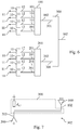
- Fig.2 shows a simplified circuit diagram for the rack (1) of Fig.1 . Going from the left side to the right side of Fig.2 , one can see:
- the rack (1) comprises four RF amplifier modules (10) and their four RF inputs (11) may for example be connected respectively to the four outputs of a 1-to-4 RF power splitter (not shown) which may or may not be mounted in or to the rack (1).
- the input of said RF power splitter may be fed with an RF signal to be amplified.
- the optional impedance adapter (50) is preferably also mounted in a volume comprised between the left-side vertical posts (7) or in a volume comprised between the right-side vertical posts (8), and at the same side (left or right) as the first RF power combiner (100), as shown in Fig.1 .
- the first combiner inputs (101) are arranged vertically, one on top of the other, and towards the front side (4) of the rack (1).
- Through holes in the front left-side post may be foreseen in order to give access to the first combiner inputs (101).
- the first combined RF power output (102) is then arranged at the back side (5) of the rack (1).
- a through hole in the rear left-side post may be foreseen in order to give access to the first combined RF power output (102).
- each RF amplifier module (10) has a front face (31) located at the front side (4) of the rack (1), and said front face (31) comprises an electrical circuit linking the amplified RF output (12) of the RF amplifier module (10) to the first RF power combiner (100).
- the said electrical circuit is a simple transmission line having a characteristic impedance Zo.
- each RF amplifier module (10) is removably mounted in the rack (1), and its front face comprises a first connector (30) to removably connect the electrical circuit to the first RF power combiner (100).
- said first connector is arranged at a distal left side of the said front face (31), in front of a corresponding first combiner input (101) having a mating connector. This allows to easily insert and remove an RF amplifier module (10) from the rack (1), for example for replacement or repair.
- each first connector (30) is preferably arranged at a distal right side of the front face of each RF amplifier module (10).
- each front face (31) is protected by a cover made of an electrically insulating material such as plastic for example.
- each RF amplifier module (10) comprises a printed circuit board with an RF amplifier circuit and a front face (31)
- said front face (31) is preferably removably mounted to said printed circuit board, and the electrical circuit of said front face (31) is connected to the amplified RF output (12) of said RF amplifier module (10) via a second connector (32).
- a second connector (32) This allows for example to test an RF amplifier module (10) without removing it from the rack (1) and without it being connected to the first power combiner.
- the first RF power combiner (100) is completely contained in the volume comprised between the left-side vertical posts (7) of the frame.
- the first RF power combiner (100) is completely contained in the volume comprised between the right-side vertical posts (8) of the frame, in which case the first connectors (30) will of course be arranged a distal right side of each RF amplifier module (10)
- Fig.3 shows an exemplary preferred embodiment of a rack according to the invention. It is similar to the rack (1) of Fig.1 , except that, in this case, the first RF power combiner (100) is spatially divided in several parts:
- Fig.4 shows a simplified circuit diagram of the rack of Fig.3 , whereon appear again the impedances (A1, A2, B, C1, C2, R1) cited hereinabove as well as the links between them and with the RF amplifier modules (10).
- the first RF power combiner (100) is a 4-to-1 "Gysel" type combiner, as described in relation to Fig.2 .
- each RF amplifier module (10) preferably comprises a third connector (33) arranged at the distal right side of the said front face (31), in addition to the first connector (30) arranged at the distal left side of the said front face, so as to be able to easily insert and remove each RF amplifier module (10) from the rack (1).
- each first connector (30) makes a link between impedances A1 and A2
- each third connector (33) makes a link between impedances C1 and C2.
- each front face (31) of each RF amplifier module (10) preferably further comprises a connection to a load R1.
- Load R1 serves as a balancing load of the Gysel combiner.
- each load R1 is part of respectively each RF amplifier module (10), which allows to save volume for the other parts of the Gysel combiner and/or for other components in the volume comprised between the left-side vertical posts (7) of the frame or in the volume comprised between the right-side vertical posts (8) of the frame.
- R1 is over-dimensioned in order to be able to test an RF amplifier module (10) on its own internal load when it is isolated from the other RF amplifier modules.
- a front face (31) comprises the second connector (32)
- said front face (31) also comprises a fourth connector (34) for connecting the load R1 to a point between impedances B and C1, as shown on Fig.3 .
- a nominal frequency range of each RF amplifier module (10) is comprised in the range of 3 MHz to 3 GHz. More preferably, a nominal frequency range of each RF amplifier module (10) is comprised in the range of 10 MHz to 300 MHz. Even more preferably, the nominal frequency of each RF amplifier module (10) is equal to 176 MHz +/- 5%.
- a nominal output power of each RF amplifier module (10) is comprised in the range of 1 KW to 100 KW. More preferably, a nominal output power of each RF amplifier module (10) is comprised in the range of 3 KW to 30 KW. Even more preferably, a nominal output power of each RF amplifier module (10) is equal to 6 KW +/- 5%.
- the first RF power combiner (100) has a number of first combiner inputs (101) which is comprised between two and ten, said first combiner inputs (101) being connected to the amplified RF outputs (12) of respectively between two and ten rack-mounted RF amplifier modules (10) to deliver the first combined RF power output (102).
- Fig.5 shows an exemplary preferred embodiment of a rack (1) according to the invention. It is similar to the rack (1) of Fig.1 , except that the rack (1) further comprises a second RF power combiner (200) whose second combiner inputs (201) are connected to the amplified RF outputs (12) of further RF amplifier modules (10) of the rack (1) to deliver a second combined RF power output (202).
- the second RF power combiner (200) is also mounted in the rack (1) in a volume comprised between the left-side vertical posts (7) of the frame, but it may alternatively be mounted in a volume comprised between the right-side vertical posts (8) of the frame or be divided as shown in Fig.3 and Fig.4 for example.
- the rack (1) then further comprises a third RF power combiner (300) whose third combiner inputs (301, 302) are connected to respectively the first and second combined RF power outputs (102, 202) of respectively the first and second RF power combiners (100, 200) to deliver a third combined RF power output (302).
- the third RF power combiner (300) is preferably mounted at the back left side or at the back right side of the rack (1), depending on where the first and second RF power combiners have their outputs.
- the third RF power combiner (300) is mounted at the back left side (2) of the rack (1) because the first and second RF power combiners (100, 200) are both mounted in a volume comprised between the left-side vertical posts (7) of the frame.
- the third RF power combiner (300) may alternatively be mounted at the back right side (3) of the rack (1) in case the first and second RF power combiners (100, 200) are mounted in a volume comprised between the right-side vertical posts (8) of the frame.
- Fig.6 shows a simplified circuit diagram for the rack (1) of Fig.5 . Going from the left side to the right side of Fig.6 , one can see:
- the third RF power combiner (300) preferably comprises a hybrid coupled line, as shown in more detail on Fig.7 .
- a hybrid coupled line is well known in the art and will therefore not be described further.
- Fig.8 shows a simplified circuit diagram of a more preferred embodiment of a rack (1) according to the invention. It is similar to the rack (1) of Fig.5 , except that the rack (1) further comprises a fourth and a fifth RF power combiner (400, 500) whose fourth and fifth combiner inputs (401, 501) are respectively connected to the amplified RF outputs (12) of further RF amplifier modules (10) of the rack (1) to deliver respectively a fourth and a fifth combined RF power output (402, 502).
- the rack (1) comprises sixteen RF amplifier modules (10) and their sixteen inputs may for example be connected respectively to the sixteen outputs of a 1 -to-16 RF power splitter (not shown) which may or may not be mounted in the rack (1). The input of said RF power splitter may be fed with a low power RF signal to be amplified.
- the fourth and fifth RF power combiners (400, 500) are mounted in the rack (1) in a volume comprised between the left-side vertical posts (7) of the frame or in a volume comprised between the right-side vertical posts (8) of the frame, or are divided as shown in Fig.3 and Fig.4 for example.
- the fourth and fifth RF power combiners (400, 500) are each for example a 4-to-1 "Gysel" type combiner as described hereinabove.
- the rack (1) further comprises a sixth RF power combiner (600) whose sixth combiner inputs (601) are connected to the fourth and fifth combined RF power outputs (402, 502) of respectively the fourth and fifth RF power combiners (400, 500) to deliver a sixth combined RF power output (602).
- the sixth RF power combiner (600) is also mounted at a back side (5) of the rack (1) and is preferably a hybrid coupled line as described hereinabove in relation to Fig.7 .
- the sixth RF power combiner (600) is mounted at a back right side (5) of the rack (1) when the third RF power combiner (300) is mounted at the back left side of the rack, and vice-versa.
- the rack (1) further comprises a seventh RF power combiner (700) whose seventh combiner inputs (701) are connected to the third and sixth combined RF power outputs (302, 602) to deliver a seventh combined RF power output (702).
- the seventh RF power combiner (700) is preferably mounted on a top of the rack (1).
- the seventh RF power combiner (700) preferably comprises a 90° hybrid power combiner of the branch line type, as schematically shown on Fig.9 . Such a power combiner is well known in the art and will therefore not be described further.
- each RF amplifier module (10) may for example have a nominal output power 6 KW for a nominal input power of 600mW.
- the indicated impedances and rated powers may - in such a 96 KW case - for example be as follows:
- the rack (1) may have any kind of suitable dimensions.
- the rack (1) according to the invention is a standard 19 inch rack (as for example defined in one of following standards : EIA 310-D, IEC 60297, CEA-310-E, DIN 41494), or a standard 21 inch rack (as for example defined in the following ETSI standard : ETS 300119), or 23 inch rack (Western Electric 23-inch standard).
- the RF amplifier modules (10) are grouped by four and there are no other types of modules between any two RF amplifier modules (10) of any group of four RF amplifier modules (10).
- a rack (1) comprising a frame having left side vertical posts (2) and right side vertical posts (3) between which a plurality of RF amplifier modules (10) are mounted.
- the RF power outputs (12) of the RF amplifier modules (10) are connected respectively to inputs (101) of an RF power combiner (100) to deliver a combined RF power output (102).
- the RF power combiner (100) is arranged at least partially in a volume comprised between the left-side vertical posts (7) of the frame or in a volume comprised between the right-side vertical posts (8) of the frame, thereby reducing the footprint of the rack (1).
Landscapes
- Engineering & Computer Science (AREA)
- Power Engineering (AREA)
- Microelectronics & Electronic Packaging (AREA)
- Aviation & Aerospace Engineering (AREA)
- Physics & Mathematics (AREA)
- Thermal Sciences (AREA)
- Amplifiers (AREA)
- Transmitters (AREA)
Claims (14)
- Rack (1) pour monter de multiples modules d'équipement, ledit rack (1) présentant un côté gauche (2), un côté droit (3) un côté avant (4), un côté arrière (5), un côté supérieur et un côté inférieur, ledit rack (1) comprenant:- un cadre présentant des montants verticaux de côté gauche (7) et des montants verticaux de côté droit (8),- une pluralité de modules d'amplificateur RF (10), qui sont montés sur le cadre entre les montants verticaux de côté gauche (7) d'une part et les montants verticaux de côté droit (8) d'autre part, chaque module d'amplificateur RF (10) comprenant un circuit d'amplificateur RF comportant une entrée RF (11) et une sortie RF amplifiée (12), et- un premier combineur de puissance RF (100) dont les premières entrées de combineur (101) sont connectées aux sorties RF amplifiées (12) des modules d'amplificateur RF (10) afin de produire une première sortie de puissance RF combinée (102),
caractérisé en ce que le premier combineur de puissance RF (100) est monté au moins partiellement à l'intérieur d'un espace qui est défini entre les montants verticaux de côté gauche (7) du cadre, ou au moins partiellement à l'intérieur d'un espace qui est défini entre les montants verticaux de côté droit (8) du cadre, en ce que chaque module d'amplificateur RF (10) présente une face avant (31) qui est située sur le côté avant (4) du rack (1), et en ce que ladite face avant (31) comprend un circuit électrique qui relie la sortie RF amplifiée (12) du module d'amplificateur RF (10) au combineur de puissance RF (100). - Rack (1) selon la revendication 1, caractérisé en ce que chaque module d'amplificateur RF (10) est monté de façon amovible dans le rack (1), et en ce que sa face avant comprend un premier connecteur (30) pour connecter de façon détachable le circuit électrique au premier combineur de puissance RF (100), ledit premier connecteur étant agencé au niveau d'un côté gauche distal ou au niveau d'un côté droit distal de ladite face avant (31).
- Rack (1) selon la revendication 1 ou 2, caractérisé en ce que chaque module d'amplificateur RF (10) comprend une carte de circuit imprimé comportant un circuit d'amplificateur RF, en ce que sa face avant (31) est montée de façon amovible sur la carte de circuit imprimé, et en ce que le circuit électrique de sa face avant (31) est connecté à la sortie RF amplifiée (12) dudit module d'amplificateur RF (10) par l'intermédiaire d'un deuxième connecteur (32).
- Rack (1) selon l'une quelconque des revendications précédentes, caractérisé en ce que le premier combineur de puissance RF (100) est contenu complètement à l'intérieur de l'espace qui est défini entre les montants verticaux de côté gauche (7) du cadre ou est contenu complètement à l'intérieur de l'espace qui est défini entre les montants verticaux de côté droit (8) du cadre.
- Rack (1) selon l'une quelconque des revendications 1 à 3, caractérisé en ce que le premier combineur de puissance RF (100) est contenu partiellement à l'intérieur de l'espace qui est défini entre les montants verticaux de côté gauche (7) du cadre et/ou est contenu partiellement à l'intérieur de l'espace qui est défini entre les montants verticaux de côté droit (8) du cadre, et en ce que la partie restante du premier combineur de puissance RF (100) est au moins partiellement agencée sur la face avant de chaque module d'amplificateur RF (10).
- Rack (1) selon l'une quelconque des revendications précédentes, caractérisé en ce que le premier combineur de puissance RF (100) est un combineur de type Gysel.
- Rack (1) selon l'une quelconque des revendications précédentes, caractérisé en ce qu'une plage de fréquence nominale de chaque module d'amplificateur RF (10) est comprise dans la gamme de 3 MHz à 3 GHz.
- Rack (1) selon l'une quelconque des revendications précédentes, caractérisé en ce qu'une puissance de sortie nominale de chaque module d'amplificateur RF (10) est comprise dans la gamme de 1 KW à 100 KW.
- Rack (1) selon la revendication 8, caractérisé en ce qu'une puissance de sortie nominale de chaque module d'amplificateur RF (10) est comprise dans la gamme de 3 KW à 30 KW.
- Rack (1) selon l'une quelconque des revendications précédentes, caractérisé en ce que le premier combineur de puissance RF (100) présente un nombre de premières entrées de combineur (101) qui est défini entre deux et dix, lesdites premières entrées de combineur (101) étant connectées aux sorties RF amplifiées (12) de respectivement entre deux et dix modules d'amplificateur RF (10) montés sur le rack afin de produire la première sortie de puissance RF combinée (102).
- Rack (1) selon l'une quelconque des revendications précédentes, caractérisé en ce que le rack (1) comprend en outre un deuxième combineur de puissance RF (200) dont les deuxièmes entrées de combineur (201) sont connectées aux sortie RF amplifiées (12) de modules d'amplificateur RF supplémentaires (10) du rack (1) afin de produire une deuxième sortie de puissance RF combinée (202), en ce que le deuxième combineur de puissance RF (200) est monté au moins partiellement à l'intérieur d'un espace qui est défini entre les montants verticaux de côté gauche (7) du cadre ou au moins partiellement à l'intérieur d'un espace qui est défini entre les montants verticaux de côté droit (8) du cadre, en ce que le rack (1) comprend en outre un troisième combineur de puissance RF (300) dont les troisièmes entrées de combineur (301) sont connectées respectivement aux première et deuxième sorties de puissance RF combinées (101, 202) de respectivement les premier et deuxième combineurs de puissance RF (100, 200) afin de produire une troisième sortie de puissance RF combinée (302), et en ce que le troisième combineur de puissance RF (300) est monté sur le côté arrière (5) du rack (1).
- Rack (1) selon la revendication 12, caractérisé en ce que le troisième combineur de puissance RF (300) comprend une ligne couplée hybride.
- Rack (1) selon la revendication 11 ou 12, caractérisé en ce que le rack (1) comprend en outre un quatrième et un cinquième combineurs de puissance RF (400, 500) dont les quatrièmes et cinquièmes entrées de combineur (401, 501) sont respectivement connectées aux sorties RF amplifiées (12) de modules d'amplificateur RF supplémentaires (10) du rack (1) afin de produire respectivement une quatrième et une cinquième sorties de puissance RF combinées (402, 502), en ce que les quatrième et cinquième combineurs de puissance RF (400, 500) sont montées au moins partiellement à l'intérieur d'un espace qui est défini entre les montants verticaux de côté gauche (7) du cadre ou au moins partiellement à l'intérieur d'un espace qui est défini entre les montants verticaux de côté droit (8) du cadre, en ce que le rack (1) comprend en outre un sixième combineur de puissance RF (600) dont les sixièmes entrées de combineur (601) sont connectées aux quatrième et cinquième sorties de puissance RF combinées (402, 502) de respectivement les quatrième et cinquième combineurs de puissance RF (400, 500) afin de produire une sixième sortie de puissance RF combinée (602), en ce que le sixième combineur de puissance RF (600) est monté sur le côté arrière (5) du rack (1), en ce que le rack (1) comprend en outre un septième combineur de puissance RF (700) dont les septièmes entrées de combineur (701) sont connectées aux troisième et sixième sorties de puissance RF combinées (302, 602) afin de produire une septième sortie de puissance RF combinée (702), et en ce que le septième combineur de puissance RF (700) est monté au sommet du rack (1).
- Rack (1) selon la revendication 13, caractérisé en ce que le sixième combineur de puissance RF (600) comprend une ligne couplée hybride, et en ce que le septième combineur de puissance RF (700) comprend un combineur de puissance hybride en quadrature (90°) du type à lignes de ramification.
Priority Applications (6)
| Application Number | Priority Date | Filing Date | Title |
|---|---|---|---|
| EP17163058.5A EP3382893B1 (fr) | 2017-03-27 | 2017-03-27 | Râtelier comprenant un amplificateur hf de haute puissance |
| ES17163058T ES2826298T3 (es) | 2017-03-27 | 2017-03-27 | Bastidor que comprende un amplificador de RF de alta potencia |
| US15/903,609 US10779433B2 (en) | 2017-03-27 | 2018-02-23 | Rack comprising a high power RF amplifier |
| JP2018058184A JP7120782B2 (ja) | 2017-03-27 | 2018-03-26 | 大電力rf増幅器を備えるラック |
| CN201810250938.7A CN108667429B (zh) | 2017-03-27 | 2018-03-26 | 包括高功率rf放大器的机架 |
| US16/943,769 US11277934B2 (en) | 2017-03-27 | 2020-07-30 | Rack comprising a high power RF amplifier |
Applications Claiming Priority (1)
| Application Number | Priority Date | Filing Date | Title |
|---|---|---|---|
| EP17163058.5A EP3382893B1 (fr) | 2017-03-27 | 2017-03-27 | Râtelier comprenant un amplificateur hf de haute puissance |
Publications (2)
| Publication Number | Publication Date |
|---|---|
| EP3382893A1 EP3382893A1 (fr) | 2018-10-03 |
| EP3382893B1 true EP3382893B1 (fr) | 2020-09-16 |
Family
ID=58428186
Family Applications (1)
| Application Number | Title | Priority Date | Filing Date |
|---|---|---|---|
| EP17163058.5A Active EP3382893B1 (fr) | 2017-03-27 | 2017-03-27 | Râtelier comprenant un amplificateur hf de haute puissance |
Country Status (5)
| Country | Link |
|---|---|
| US (2) | US10779433B2 (fr) |
| EP (1) | EP3382893B1 (fr) |
| JP (1) | JP7120782B2 (fr) |
| CN (1) | CN108667429B (fr) |
| ES (1) | ES2826298T3 (fr) |
Families Citing this family (5)
| Publication number | Priority date | Publication date | Assignee | Title |
|---|---|---|---|---|
| EP3382893B1 (fr) * | 2017-03-27 | 2020-09-16 | Ion Beam Applications | Râtelier comprenant un amplificateur hf de haute puissance |
| WO2018216073A1 (fr) * | 2017-05-22 | 2018-11-29 | 三菱電機株式会社 | Machine électronique |
| KR200495933Y1 (ko) * | 2021-03-09 | 2022-09-26 | 주식회사 한진전자산업 | 이로란 신호 송신 장치 |
| CN114630531B (zh) * | 2022-03-24 | 2024-03-26 | 石家庄信科微波技术有限公司 | 一种新型功率放大器 |
| KR102598866B1 (ko) * | 2023-07-31 | 2023-11-07 | ㈜알에프피티 | 판상형 전력증폭기 |
Citations (1)
| Publication number | Priority date | Publication date | Assignee | Title |
|---|---|---|---|---|
| JPS57125505A (en) * | 1981-01-29 | 1982-08-04 | Fujitsu Ltd | Ultrahigh frequency amplifier |
Family Cites Families (28)
| Publication number | Priority date | Publication date | Assignee | Title |
|---|---|---|---|---|
| JPS63158905A (ja) * | 1986-12-23 | 1988-07-01 | Tokyo Keiki Co Ltd | 高周波電力増幅装置 |
| JP2830664B2 (ja) * | 1992-12-11 | 1998-12-02 | 富士通株式会社 | 通信ユニット |
| JPH06350274A (ja) * | 1993-06-04 | 1994-12-22 | Fujitsu Ltd | 通信装置 |
| JPH08330769A (ja) * | 1995-05-31 | 1996-12-13 | Fujitsu Ltd | 通信装置のキャビネット構造 |
| US5737194A (en) * | 1996-07-29 | 1998-04-07 | Cray Research, Inc. | Input/output module assembly |
| US6185109B1 (en) * | 1999-02-26 | 2001-02-06 | 3Com Corporation | Electronic chassis apparatus and method |
| US6195493B1 (en) * | 1999-05-21 | 2001-02-27 | Scientific-Atlanta, Inc. | Universal chassis for CATV headends or telecommunications company central office for optical electronic equipment |
| US6549405B2 (en) * | 2000-06-09 | 2003-04-15 | Vertex Electronic Products, Inc. | Electronic chassis |
| US7046101B2 (en) * | 2001-06-29 | 2006-05-16 | L-3 Communications | Switchable RF power divider/combiner with switchable impedance matching elements |
| US6842348B2 (en) * | 2002-05-31 | 2005-01-11 | Pci Technologies, Inc. | RF circuit modules and integrated chassis with power interface for RF circuit modules |
| JP2006286301A (ja) * | 2005-03-31 | 2006-10-19 | Toshiba Corp | 高周波電力増幅装置 |
| US7719848B2 (en) * | 2005-04-27 | 2010-05-18 | Motorola, Inc. | Base radios with interchangeable modules |
| US7647044B2 (en) * | 2005-08-24 | 2010-01-12 | Atx Networks Corp. | RF switching device |
| JP4831000B2 (ja) * | 2007-07-20 | 2011-12-07 | ヤマハ株式会社 | ラックマウント用電子機器 |
| JP4528838B2 (ja) * | 2008-02-22 | 2010-08-25 | 株式会社東芝 | 電力増幅装置及びこの電力増幅装置を用いた送信機 |
| US8411447B2 (en) * | 2009-12-18 | 2013-04-02 | Teledyne Paradise Datacom, Llc | Power amplifier chassis |
| US8189338B2 (en) * | 2009-12-18 | 2012-05-29 | Paradise Datacom, LLC | Power amplifier system |
| JP2012100020A (ja) * | 2010-11-01 | 2012-05-24 | Toshiba Corp | 電力増幅装置 |
| CN201966924U (zh) * | 2011-04-20 | 2011-09-07 | 嘉兴市科讯电子有限公司 | 公共广播主机 |
| CN103376824B (zh) * | 2012-04-23 | 2016-05-18 | 纬创资通股份有限公司 | 储存装置组装模块及电子装置 |
| EP2980990B1 (fr) * | 2013-03-26 | 2019-01-02 | Nec Corporation | Amplificateur de puissance |
| EP3011632A1 (fr) * | 2013-08-15 | 2016-04-27 | Siemens, LLC | Dispositif pour couplage de puissance par radiofréquence et son procédé d'utilisation |
| EP3011633A1 (fr) | 2013-08-15 | 2016-04-27 | Siemens, LLC | Ensemble pour couplage de puissance par radiofréquence (rf) et son procédé d'utilisation |
| US9496831B2 (en) * | 2014-10-17 | 2016-11-15 | Daico Industries, Inc. | Combined high power rf/microwave amplifier with multiple power amplifier units and automatic failure protection |
| WO2016089245A1 (fr) * | 2014-12-05 | 2016-06-09 | Siemens Research Center Limited Liability Company | Combinateur de puissance rf modifié |
| CN115932685A (zh) * | 2015-08-21 | 2023-04-07 | 皇家飞利浦有限公司 | 用于磁共振系统中的核激励的rf信号的生成 |
| CN205754223U (zh) * | 2016-06-18 | 2016-11-30 | 上海觉浅广播器材有限公司 | 一种小型化调频大功率放大器 |
| EP3382893B1 (fr) * | 2017-03-27 | 2020-09-16 | Ion Beam Applications | Râtelier comprenant un amplificateur hf de haute puissance |
-
2017
- 2017-03-27 EP EP17163058.5A patent/EP3382893B1/fr active Active
- 2017-03-27 ES ES17163058T patent/ES2826298T3/es active Active
-
2018
- 2018-02-23 US US15/903,609 patent/US10779433B2/en active Active
- 2018-03-26 CN CN201810250938.7A patent/CN108667429B/zh active Active
- 2018-03-26 JP JP2018058184A patent/JP7120782B2/ja active Active
-
2020
- 2020-07-30 US US16/943,769 patent/US11277934B2/en active Active
Patent Citations (1)
| Publication number | Priority date | Publication date | Assignee | Title |
|---|---|---|---|---|
| JPS57125505A (en) * | 1981-01-29 | 1982-08-04 | Fujitsu Ltd | Ultrahigh frequency amplifier |
Also Published As
| Publication number | Publication date |
|---|---|
| US20200359522A1 (en) | 2020-11-12 |
| ES2826298T3 (es) | 2021-05-18 |
| CN108667429A (zh) | 2018-10-16 |
| JP2018164256A (ja) | 2018-10-18 |
| JP7120782B2 (ja) | 2022-08-17 |
| US11277934B2 (en) | 2022-03-15 |
| US20180279499A1 (en) | 2018-09-27 |
| EP3382893A1 (fr) | 2018-10-03 |
| US10779433B2 (en) | 2020-09-15 |
| CN108667429B (zh) | 2023-05-09 |
Similar Documents
| Publication | Publication Date | Title |
|---|---|---|
| US11277934B2 (en) | Rack comprising a high power RF amplifier | |
| US9595930B2 (en) | Solid state microwave generator and power amplifier | |
| US6069797A (en) | Power distribution assembly | |
| FI90812C (fi) | Elektroninen järjestelmä | |
| EP3249811A1 (fr) | Amplificateurs d'hyperfréquences/rf combinés comportant des alimentations individuelles | |
| US7555309B2 (en) | Radio frequency router | |
| US9647958B2 (en) | Radio frequency signal router | |
| US9477851B2 (en) | LCL high power combiner | |
| KR101841723B1 (ko) | 무선-주파수(rf) 전력 커플링을 위한 어셈블리 및 그 어셈블리를 사용하는 방법 | |
| KR20160058775A (ko) | 라디오-주파수 전력 커플링을 위한 디바이스 및 상기 디바이스를 사용하는 방법 | |
| CN217823210U (zh) | 一种650MHz Gysel多路径向功率合成器 | |
| US20240195061A1 (en) | Advanced antenna architecture with low pim | |
| CN109361362A (zh) | 一种固态高功率放大器 | |
| US7570132B1 (en) | Switch matrix | |
| US20170346150A1 (en) | Modified Radio Frequency (RF) Combiner | |
| JP7565085B2 (ja) | 増幅モジュールが外側導体上に配置された高周波増幅ユニット | |
| RU181024U1 (ru) | Конструкция радиочастотного объединителя с ключами | |
| US20020030980A1 (en) | Densely arranged electrically shielded communication panels | |
| KR20250023115A (ko) | 평형 증폭기 | |
| PL64791Y1 (pl) | Konstrukcja modułu nadawczego |
Legal Events
| Date | Code | Title | Description |
|---|---|---|---|
| PUAI | Public reference made under article 153(3) epc to a published international application that has entered the european phase |
Free format text: ORIGINAL CODE: 0009012 |
|
| STAA | Information on the status of an ep patent application or granted ep patent |
Free format text: STATUS: THE APPLICATION HAS BEEN PUBLISHED |
|
| AK | Designated contracting states |
Kind code of ref document: A1 Designated state(s): AL AT BE BG CH CY CZ DE DK EE ES FI FR GB GR HR HU IE IS IT LI LT LU LV MC MK MT NL NO PL PT RO RS SE SI SK SM TR |
|
| AX | Request for extension of the european patent |
Extension state: BA ME |
|
| STAA | Information on the status of an ep patent application or granted ep patent |
Free format text: STATUS: REQUEST FOR EXAMINATION WAS MADE |
|
| STAA | Information on the status of an ep patent application or granted ep patent |
Free format text: STATUS: EXAMINATION IS IN PROGRESS |
|
| 17P | Request for examination filed |
Effective date: 20190221 |
|
| RBV | Designated contracting states (corrected) |
Designated state(s): AL AT BE BG CH CY CZ DE DK EE ES FI FR GB GR HR HU IE IS IT LI LT LU LV MC MK MT NL NO PL PT RO RS SE SI SK SM TR |
|
| 17Q | First examination report despatched |
Effective date: 20190319 |
|
| GRAP | Despatch of communication of intention to grant a patent |
Free format text: ORIGINAL CODE: EPIDOSNIGR1 |
|
| STAA | Information on the status of an ep patent application or granted ep patent |
Free format text: STATUS: GRANT OF PATENT IS INTENDED |
|
| INTG | Intention to grant announced |
Effective date: 20200428 |
|
| GRAS | Grant fee paid |
Free format text: ORIGINAL CODE: EPIDOSNIGR3 |
|
| GRAA | (expected) grant |
Free format text: ORIGINAL CODE: 0009210 |
|
| STAA | Information on the status of an ep patent application or granted ep patent |
Free format text: STATUS: THE PATENT HAS BEEN GRANTED |
|
| AK | Designated contracting states |
Kind code of ref document: B1 Designated state(s): AL AT BE BG CH CY CZ DE DK EE ES FI FR GB GR HR HU IE IS IT LI LT LU LV MC MK MT NL NO PL PT RO RS SE SI SK SM TR |
|
| REG | Reference to a national code |
Ref country code: GB Ref legal event code: FG4D |
|
| REG | Reference to a national code |
Ref country code: CH Ref legal event code: EP |
|
| REG | Reference to a national code |
Ref country code: DE Ref legal event code: R096 Ref document number: 602017023606 Country of ref document: DE |
|
| REG | Reference to a national code |
Ref country code: IE Ref legal event code: FG4D |
|
| REG | Reference to a national code |
Ref country code: AT Ref legal event code: REF Ref document number: 1315065 Country of ref document: AT Kind code of ref document: T Effective date: 20201015 |
|
| REG | Reference to a national code |
Ref country code: SE Ref legal event code: TRGR |
|
| PG25 | Lapsed in a contracting state [announced via postgrant information from national office to epo] |
Ref country code: FI Free format text: LAPSE BECAUSE OF FAILURE TO SUBMIT A TRANSLATION OF THE DESCRIPTION OR TO PAY THE FEE WITHIN THE PRESCRIBED TIME-LIMIT Effective date: 20200916 Ref country code: GR Free format text: LAPSE BECAUSE OF FAILURE TO SUBMIT A TRANSLATION OF THE DESCRIPTION OR TO PAY THE FEE WITHIN THE PRESCRIBED TIME-LIMIT Effective date: 20201217 Ref country code: HR Free format text: LAPSE BECAUSE OF FAILURE TO SUBMIT A TRANSLATION OF THE DESCRIPTION OR TO PAY THE FEE WITHIN THE PRESCRIBED TIME-LIMIT Effective date: 20200916 Ref country code: NO Free format text: LAPSE BECAUSE OF FAILURE TO SUBMIT A TRANSLATION OF THE DESCRIPTION OR TO PAY THE FEE WITHIN THE PRESCRIBED TIME-LIMIT Effective date: 20201216 Ref country code: BG Free format text: LAPSE BECAUSE OF FAILURE TO SUBMIT A TRANSLATION OF THE DESCRIPTION OR TO PAY THE FEE WITHIN THE PRESCRIBED TIME-LIMIT Effective date: 20201216 |
|
| REG | Reference to a national code |
Ref country code: AT Ref legal event code: MK05 Ref document number: 1315065 Country of ref document: AT Kind code of ref document: T Effective date: 20200916 |
|
| REG | Reference to a national code |
Ref country code: NL Ref legal event code: MP Effective date: 20200916 |
|
| PG25 | Lapsed in a contracting state [announced via postgrant information from national office to epo] |
Ref country code: LV Free format text: LAPSE BECAUSE OF FAILURE TO SUBMIT A TRANSLATION OF THE DESCRIPTION OR TO PAY THE FEE WITHIN THE PRESCRIBED TIME-LIMIT Effective date: 20200916 Ref country code: RS Free format text: LAPSE BECAUSE OF FAILURE TO SUBMIT A TRANSLATION OF THE DESCRIPTION OR TO PAY THE FEE WITHIN THE PRESCRIBED TIME-LIMIT Effective date: 20200916 |
|
| REG | Reference to a national code |
Ref country code: LT Ref legal event code: MG4D |
|
| PG25 | Lapsed in a contracting state [announced via postgrant information from national office to epo] |
Ref country code: EE Free format text: LAPSE BECAUSE OF FAILURE TO SUBMIT A TRANSLATION OF THE DESCRIPTION OR TO PAY THE FEE WITHIN THE PRESCRIBED TIME-LIMIT Effective date: 20200916 Ref country code: SM Free format text: LAPSE BECAUSE OF FAILURE TO SUBMIT A TRANSLATION OF THE DESCRIPTION OR TO PAY THE FEE WITHIN THE PRESCRIBED TIME-LIMIT Effective date: 20200916 Ref country code: LT Free format text: LAPSE BECAUSE OF FAILURE TO SUBMIT A TRANSLATION OF THE DESCRIPTION OR TO PAY THE FEE WITHIN THE PRESCRIBED TIME-LIMIT Effective date: 20200916 Ref country code: PT Free format text: LAPSE BECAUSE OF FAILURE TO SUBMIT A TRANSLATION OF THE DESCRIPTION OR TO PAY THE FEE WITHIN THE PRESCRIBED TIME-LIMIT Effective date: 20210118 Ref country code: RO Free format text: LAPSE BECAUSE OF FAILURE TO SUBMIT A TRANSLATION OF THE DESCRIPTION OR TO PAY THE FEE WITHIN THE PRESCRIBED TIME-LIMIT Effective date: 20200916 Ref country code: CZ Free format text: LAPSE BECAUSE OF FAILURE TO SUBMIT A TRANSLATION OF THE DESCRIPTION OR TO PAY THE FEE WITHIN THE PRESCRIBED TIME-LIMIT Effective date: 20200916 |
|
| REG | Reference to a national code |
Ref country code: ES Ref legal event code: FG2A Ref document number: 2826298 Country of ref document: ES Kind code of ref document: T3 Effective date: 20210518 |
|
| PG25 | Lapsed in a contracting state [announced via postgrant information from national office to epo] |
Ref country code: IS Free format text: LAPSE BECAUSE OF FAILURE TO SUBMIT A TRANSLATION OF THE DESCRIPTION OR TO PAY THE FEE WITHIN THE PRESCRIBED TIME-LIMIT Effective date: 20210116 Ref country code: PL Free format text: LAPSE BECAUSE OF FAILURE TO SUBMIT A TRANSLATION OF THE DESCRIPTION OR TO PAY THE FEE WITHIN THE PRESCRIBED TIME-LIMIT Effective date: 20200916 Ref country code: AL Free format text: LAPSE BECAUSE OF FAILURE TO SUBMIT A TRANSLATION OF THE DESCRIPTION OR TO PAY THE FEE WITHIN THE PRESCRIBED TIME-LIMIT Effective date: 20200916 Ref country code: AT Free format text: LAPSE BECAUSE OF FAILURE TO SUBMIT A TRANSLATION OF THE DESCRIPTION OR TO PAY THE FEE WITHIN THE PRESCRIBED TIME-LIMIT Effective date: 20200916 |
|
| REG | Reference to a national code |
Ref country code: DE Ref legal event code: R097 Ref document number: 602017023606 Country of ref document: DE |
|
| PG25 | Lapsed in a contracting state [announced via postgrant information from national office to epo] |
Ref country code: SK Free format text: LAPSE BECAUSE OF FAILURE TO SUBMIT A TRANSLATION OF THE DESCRIPTION OR TO PAY THE FEE WITHIN THE PRESCRIBED TIME-LIMIT Effective date: 20200916 |
|
| PLBE | No opposition filed within time limit |
Free format text: ORIGINAL CODE: 0009261 |
|
| STAA | Information on the status of an ep patent application or granted ep patent |
Free format text: STATUS: NO OPPOSITION FILED WITHIN TIME LIMIT |
|
| 26N | No opposition filed |
Effective date: 20210617 |
|
| PG25 | Lapsed in a contracting state [announced via postgrant information from national office to epo] |
Ref country code: DK Free format text: LAPSE BECAUSE OF FAILURE TO SUBMIT A TRANSLATION OF THE DESCRIPTION OR TO PAY THE FEE WITHIN THE PRESCRIBED TIME-LIMIT Effective date: 20200916 Ref country code: SI Free format text: LAPSE BECAUSE OF FAILURE TO SUBMIT A TRANSLATION OF THE DESCRIPTION OR TO PAY THE FEE WITHIN THE PRESCRIBED TIME-LIMIT Effective date: 20200916 |
|
| PG25 | Lapsed in a contracting state [announced via postgrant information from national office to epo] |
Ref country code: MC Free format text: LAPSE BECAUSE OF FAILURE TO SUBMIT A TRANSLATION OF THE DESCRIPTION OR TO PAY THE FEE WITHIN THE PRESCRIBED TIME-LIMIT Effective date: 20200916 |
|
| GBPC | Gb: european patent ceased through non-payment of renewal fee |
Effective date: 20210327 |
|
| PG25 | Lapsed in a contracting state [announced via postgrant information from national office to epo] |
Ref country code: GB Free format text: LAPSE BECAUSE OF NON-PAYMENT OF DUE FEES Effective date: 20210327 Ref country code: IE Free format text: LAPSE BECAUSE OF NON-PAYMENT OF DUE FEES Effective date: 20210327 Ref country code: LU Free format text: LAPSE BECAUSE OF NON-PAYMENT OF DUE FEES Effective date: 20210327 |
|
| P01 | Opt-out of the competence of the unified patent court (upc) registered |
Effective date: 20230427 |
|
| PG25 | Lapsed in a contracting state [announced via postgrant information from national office to epo] |
Ref country code: NL Free format text: LAPSE BECAUSE OF NON-PAYMENT OF DUE FEES Effective date: 20200923 Ref country code: CY Free format text: LAPSE BECAUSE OF FAILURE TO SUBMIT A TRANSLATION OF THE DESCRIPTION OR TO PAY THE FEE WITHIN THE PRESCRIBED TIME-LIMIT Effective date: 20200916 |
|
| PG25 | Lapsed in a contracting state [announced via postgrant information from national office to epo] |
Ref country code: HU Free format text: LAPSE BECAUSE OF FAILURE TO SUBMIT A TRANSLATION OF THE DESCRIPTION OR TO PAY THE FEE WITHIN THE PRESCRIBED TIME-LIMIT; INVALID AB INITIO Effective date: 20170327 |
|
| PG25 | Lapsed in a contracting state [announced via postgrant information from national office to epo] |
Ref country code: MK Free format text: LAPSE BECAUSE OF FAILURE TO SUBMIT A TRANSLATION OF THE DESCRIPTION OR TO PAY THE FEE WITHIN THE PRESCRIBED TIME-LIMIT Effective date: 20200916 |
|
| PG25 | Lapsed in a contracting state [announced via postgrant information from national office to epo] |
Ref country code: MT Free format text: LAPSE BECAUSE OF FAILURE TO SUBMIT A TRANSLATION OF THE DESCRIPTION OR TO PAY THE FEE WITHIN THE PRESCRIBED TIME-LIMIT Effective date: 20200916 |
|
| PGFP | Annual fee paid to national office [announced via postgrant information from national office to epo] |
Ref country code: ES Payment date: 20250401 Year of fee payment: 9 |
|
| PGFP | Annual fee paid to national office [announced via postgrant information from national office to epo] |
Ref country code: CH Payment date: 20250401 Year of fee payment: 9 |
|
| PG25 | Lapsed in a contracting state [announced via postgrant information from national office to epo] |
Ref country code: TR Free format text: LAPSE BECAUSE OF FAILURE TO SUBMIT A TRANSLATION OF THE DESCRIPTION OR TO PAY THE FEE WITHIN THE PRESCRIBED TIME-LIMIT Effective date: 20200916 |
|
| REG | Reference to a national code |
Ref country code: CH Ref legal event code: U11 Free format text: ST27 STATUS EVENT CODE: U-0-0-U10-U11 (AS PROVIDED BY THE NATIONAL OFFICE) Effective date: 20260401 |
|
| PGFP | Annual fee paid to national office [announced via postgrant information from national office to epo] |
Ref country code: SE Payment date: 20260327 Year of fee payment: 10 |
|
| PGFP | Annual fee paid to national office [announced via postgrant information from national office to epo] |
Ref country code: DE Payment date: 20260327 Year of fee payment: 10 |
|
| PGFP | Annual fee paid to national office [announced via postgrant information from national office to epo] |
Ref country code: BE Payment date: 20260327 Year of fee payment: 10 Ref country code: IT Payment date: 20260319 Year of fee payment: 10 |
|
| PGFP | Annual fee paid to national office [announced via postgrant information from national office to epo] |
Ref country code: FR Payment date: 20260325 Year of fee payment: 10 |