EP3386101A1 - Multimodales leistungsverstärkermodul, chip und kommunikationsendgerät - Google Patents
Multimodales leistungsverstärkermodul, chip und kommunikationsendgerät Download PDFInfo
- Publication number
- EP3386101A1 EP3386101A1 EP16870015.1A EP16870015A EP3386101A1 EP 3386101 A1 EP3386101 A1 EP 3386101A1 EP 16870015 A EP16870015 A EP 16870015A EP 3386101 A1 EP3386101 A1 EP 3386101A1
- Authority
- EP
- European Patent Office
- Prior art keywords
- frequency
- power amplifier
- signal
- low
- offset
- Prior art date
- Legal status (The legal status is an assumption and is not a legal conclusion. Google has not performed a legal analysis and makes no representation as to the accuracy of the status listed.)
- Ceased
Links
Images


Classifications
-
- H—ELECTRICITY
- H03—ELECTRONIC CIRCUITRY
- H03F—AMPLIFIERS
- H03F1/00—Details of amplifiers with only discharge tubes, only semiconductor devices or only unspecified devices as amplifying elements
- H03F1/32—Modifications of amplifiers to reduce non-linear distortion
-
- H—ELECTRICITY
- H03—ELECTRONIC CIRCUITRY
- H03F—AMPLIFIERS
- H03F1/00—Details of amplifiers with only discharge tubes, only semiconductor devices or only unspecified devices as amplifying elements
- H03F1/02—Modifications of amplifiers to raise the efficiency, e.g. gliding Class A stages, use of an auxiliary oscillation
- H03F1/0205—Modifications of amplifiers to raise the efficiency, e.g. gliding Class A stages, use of an auxiliary oscillation in transistor amplifiers
- H03F1/0211—Modifications of amplifiers to raise the efficiency, e.g. gliding Class A stages, use of an auxiliary oscillation in transistor amplifiers with control of the supply voltage or current
- H03F1/0216—Continuous control
-
- H—ELECTRICITY
- H03—ELECTRONIC CIRCUITRY
- H03F—AMPLIFIERS
- H03F1/00—Details of amplifiers with only discharge tubes, only semiconductor devices or only unspecified devices as amplifying elements
- H03F1/02—Modifications of amplifiers to raise the efficiency, e.g. gliding Class A stages, use of an auxiliary oscillation
- H03F1/0205—Modifications of amplifiers to raise the efficiency, e.g. gliding Class A stages, use of an auxiliary oscillation in transistor amplifiers
- H03F1/0211—Modifications of amplifiers to raise the efficiency, e.g. gliding Class A stages, use of an auxiliary oscillation in transistor amplifiers with control of the supply voltage or current
- H03F1/0244—Stepped control
-
- H—ELECTRICITY
- H03—ELECTRONIC CIRCUITRY
- H03F—AMPLIFIERS
- H03F1/00—Details of amplifiers with only discharge tubes, only semiconductor devices or only unspecified devices as amplifying elements
- H03F1/02—Modifications of amplifiers to raise the efficiency, e.g. gliding Class A stages, use of an auxiliary oscillation
- H03F1/0205—Modifications of amplifiers to raise the efficiency, e.g. gliding Class A stages, use of an auxiliary oscillation in transistor amplifiers
- H03F1/0261—Modifications of amplifiers to raise the efficiency, e.g. gliding Class A stages, use of an auxiliary oscillation in transistor amplifiers with control of the polarisation voltage or current, e.g. gliding Class A
-
- H—ELECTRICITY
- H03—ELECTRONIC CIRCUITRY
- H03F—AMPLIFIERS
- H03F1/00—Details of amplifiers with only discharge tubes, only semiconductor devices or only unspecified devices as amplifying elements
- H03F1/02—Modifications of amplifiers to raise the efficiency, e.g. gliding Class A stages, use of an auxiliary oscillation
- H03F1/0205—Modifications of amplifiers to raise the efficiency, e.g. gliding Class A stages, use of an auxiliary oscillation in transistor amplifiers
- H03F1/0277—Selecting one or more amplifiers from a plurality of amplifiers
-
- H—ELECTRICITY
- H03—ELECTRONIC CIRCUITRY
- H03F—AMPLIFIERS
- H03F1/00—Details of amplifiers with only discharge tubes, only semiconductor devices or only unspecified devices as amplifying elements
- H03F1/42—Modifications of amplifiers to extend the bandwidth
-
- H—ELECTRICITY
- H03—ELECTRONIC CIRCUITRY
- H03F—AMPLIFIERS
- H03F1/00—Details of amplifiers with only discharge tubes, only semiconductor devices or only unspecified devices as amplifying elements
- H03F1/56—Modifications of input or output impedances, not otherwise provided for
-
- H—ELECTRICITY
- H03—ELECTRONIC CIRCUITRY
- H03F—AMPLIFIERS
- H03F3/00—Amplifiers with only discharge tubes or only semiconductor devices as amplifying elements
- H03F3/189—High-frequency amplifiers, e.g. radio frequency amplifiers
- H03F3/19—High-frequency amplifiers, e.g. radio frequency amplifiers with semiconductor devices only
- H03F3/195—High-frequency amplifiers, e.g. radio frequency amplifiers with semiconductor devices only in integrated circuits
-
- H—ELECTRICITY
- H03—ELECTRONIC CIRCUITRY
- H03F—AMPLIFIERS
- H03F3/00—Amplifiers with only discharge tubes or only semiconductor devices as amplifying elements
- H03F3/20—Power amplifiers, e.g. Class B amplifiers, Class C amplifiers
- H03F3/21—Power amplifiers, e.g. Class B amplifiers, Class C amplifiers with semiconductor devices only
- H03F3/213—Power amplifiers, e.g. Class B amplifiers, Class C amplifiers with semiconductor devices only in integrated circuits
-
- H—ELECTRICITY
- H03—ELECTRONIC CIRCUITRY
- H03F—AMPLIFIERS
- H03F3/00—Amplifiers with only discharge tubes or only semiconductor devices as amplifying elements
- H03F3/20—Power amplifiers, e.g. Class B amplifiers, Class C amplifiers
- H03F3/24—Power amplifiers, e.g. Class B amplifiers, Class C amplifiers of transmitter output stages
- H03F3/245—Power amplifiers, e.g. Class B amplifiers, Class C amplifiers of transmitter output stages with semiconductor devices only
-
- H—ELECTRICITY
- H03—ELECTRONIC CIRCUITRY
- H03G—CONTROL OF AMPLIFICATION
- H03G1/00—Details of arrangements for controlling amplification
- H03G1/0005—Circuits characterised by the type of controlling devices operated by a controlling current or voltage signal
- H03G1/0088—Circuits characterised by the type of controlling devices operated by a controlling current or voltage signal using discontinuously variable devices, e.g. switch-operated
-
- H—ELECTRICITY
- H03—ELECTRONIC CIRCUITRY
- H03G—CONTROL OF AMPLIFICATION
- H03G3/00—Gain control in amplifiers or frequency changers
- H03G3/20—Automatic control
- H03G3/30—Automatic control in amplifiers having semiconductor devices
- H03G3/3036—Automatic control in amplifiers having semiconductor devices in high-frequency amplifiers or in frequency-changers
- H03G3/3042—Automatic control in amplifiers having semiconductor devices in high-frequency amplifiers or in frequency-changers in modulators, frequency-changers, transmitters or power amplifiers
-
- H—ELECTRICITY
- H04—ELECTRIC COMMUNICATION TECHNIQUE
- H04B—TRANSMISSION
- H04B1/00—Details of transmission systems, not covered by a single one of groups H04B3/00 - H04B13/00; Details of transmission systems not characterised by the medium used for transmission
- H04B1/02—Transmitters
- H04B1/04—Circuits
-
- H—ELECTRICITY
- H03—ELECTRONIC CIRCUITRY
- H03F—AMPLIFIERS
- H03F2200/00—Indexing scheme relating to amplifiers
- H03F2200/111—Indexing scheme relating to amplifiers the amplifier being a dual or triple band amplifier, e.g. 900 and 1800 MHz, e.g. switched or not switched, simultaneously or not
-
- H—ELECTRICITY
- H03—ELECTRONIC CIRCUITRY
- H03F—AMPLIFIERS
- H03F2200/00—Indexing scheme relating to amplifiers
- H03F2200/222—A circuit being added at the input of an amplifier to adapt the input impedance of the amplifier
-
- H—ELECTRICITY
- H03—ELECTRONIC CIRCUITRY
- H03F—AMPLIFIERS
- H03F2200/00—Indexing scheme relating to amplifiers
- H03F2200/387—A circuit being added at the output of an amplifier to adapt the output impedance of the amplifier
-
- H—ELECTRICITY
- H03—ELECTRONIC CIRCUITRY
- H03F—AMPLIFIERS
- H03F2200/00—Indexing scheme relating to amplifiers
- H03F2200/429—Two or more amplifiers or one amplifier with filters for different frequency bands are coupled in parallel at the input or output
-
- H—ELECTRICITY
- H03—ELECTRONIC CIRCUITRY
- H03F—AMPLIFIERS
- H03F2200/00—Indexing scheme relating to amplifiers
- H03F2200/451—Indexing scheme relating to amplifiers the amplifier being a radio frequency amplifier
-
- H—ELECTRICITY
- H03—ELECTRONIC CIRCUITRY
- H03G—CONTROL OF AMPLIFICATION
- H03G2201/00—Indexing scheme relating to subclass H03G
- H03G2201/40—Combined gain and bias control
-
- H—ELECTRICITY
- H04—ELECTRIC COMMUNICATION TECHNIQUE
- H04B—TRANSMISSION
- H04B1/00—Details of transmission systems, not covered by a single one of groups H04B3/00 - H04B13/00; Details of transmission systems not characterised by the medium used for transmission
- H04B1/02—Transmitters
- H04B1/04—Circuits
- H04B2001/0408—Circuits with power amplifiers
Definitions
- the present invention relates to a multimode power amplifier module, a method for controlling the multimode power amplifier module, and a chip and a communication terminal that include the multimode power amplifier module, and belongs to the field of wireless communication technologies.
- VoLTE relates to relatively many new technologies and requires necessary tests and experiments, and on the other hand, deployment and integration of an IMS (IP multimedia subsystem) takes some time, and a device of an existing network also needs to be upgraded and improved step by step.
- IMS IP multimedia subsystem
- an LTE network cannot provide an audio service.
- An audio part needs to use a 3G/2G network.
- 3GWCDMA/CDMA relates to a problem of patent fees of Qualcomm, a platform manufacturer, for example, Media Tek, Spreadtrum, and Leadcore Technology all launch a solution of applying 2G to an audio part. Therefore, 2GGSM is indispensable within quite a long time in 4G communication.
- mobile operators are making great efforts to promote three-mode and five-mode solutions.
- Three modes are mainly GSM/TD_SCDMA/TDD_LTE.
- Five modes are mainly GSM/TD_SCDMA/TDD_LTE/WCDMA/FDD_LTE. It is not hard to see that three modes and five modes are both inseparable from several modes: GSM/EDGE/TD_SCDMA/TDD_LTE.
- TD-SCDMA and TDD-LTE are mainly used for data transmission. Therefore, power consumption is a relatively serious problem.
- Power consumption of a multimode power amplifier module mainly focuses on a power amplifier. If performance and power consumption optimization of a power amplification chip can be performed in the two time-division multiplexing modes, performance and power consumption of the multimode power amplifier module can be optimized.
- a primary technical solution to be resolved by the present invention is to provide a multimode power amplifier module.
- Another technical solution to be resolved by the present invention is to provide a method for controlling a multimode power amplifier module.
- Still another technical solution to be resolved by the present invention is to provide a chip and a communication terminal that include a multimode power amplifier module.
- the multimode power amplifier module supports a GSM, EDGE, TD_SCDMA, and/or a TDD_LTE working mode; and the low-frequency input matching network is used to access a low-frequency GSM signal or a low-frequency EDGE signal; and the high-frequency input matching network is used to access a high-frequency GSM signal, a high-frequency EDGE signal, a TD_SCDMA signal, or a TDD_LTE signal.
- the amplifier control signal sent by the control circuit to the low-frequency power amplifier or the high-frequency power amplifier includes: a logic signal Vmode, an offset signal Reg, and/or a collector voltage Vcc.
- a feedback circuit is disposed in the low-frequency power amplifier or the high-frequency power amplifier; the logic signal Vmode is used to control a feedback switch on the feedback circuit to be opened or closed; when the logic signal Vmode controls the feedback switch to be opened, the low-frequency power amplifier or the high-frequency power amplifier works in a high gain mode; and when the logic signal Vmode controls the feedback switch to be closed, the low-frequency power amplifier or the high-frequency power amplifier works in a low gain mode.
- the collector voltage Vcc is used to supply power to the low-frequency power amplifier or the high-frequency power amplifier, to control an output power of the low-frequency radio frequency signal or the high-frequency radio frequency signal amplified by the low-frequency power amplifier or the high-frequency power amplifier; and the control circuit selects a corresponding basis voltage according to the working mode selection signal and generates the collector voltage Vcc according to the basis voltage.
- the control circuit selects the baseband signal Vramp as the basis voltage, to generate the collector voltage Vcc; and when the working mode selection signal is in an EDGE, TD_SCDMA, or TDD_LTE mode, the control circuit selects a reference voltage Vref as the basis voltage, to generate the collector voltage Vcc, where the reference voltage Vref and the control power supply Vbat linearly change.
- the offset signal Reg is used to adjust a current of the low-frequency power amplifier or the high-frequency power amplifier; and the control circuit closes a corresponding switch in an offset signal switch group according to the working mode selection signal, to generate an offset signal Reg corresponding to a working mode; and switches corresponding to the working modes are disposed in the offset signal switch group.
- the control circuit includes an offset signal generation circuit;
- the offset signal generation circuit includes: an operational amplifier, a p-channel metal-oxide-semiconductor field-effect transistor (PMOS), and the offset signal switch group; a positive input end of the operational amplifier accesses the reference voltage Vref; an output end of the operational amplifier is connected to a gate of the p-channel metal-oxide-semiconductor field-effect transistor (PMOS); a source of the PMOS accesses the control power supply Vbat; and a drain of the PMOS is an output end of the offset signal generation circuit and is used to output the offset signal Reg;
- the offset signal switch group is connected between a negative input end of the operational amplifier and a resistor; and resistors are connected in series between the switches in the offset signal switch group.
- the offset signals Reg corresponding to the GSM, EDGE, TDD_LTE, and TD_SCDMA working modes are sequentially reduced.
- the offset signal Reg accesses an offset circuit of a power amplifier;
- the offset circuit includes R71, D71, D72, and a collector of a Q71 biopolar transistor; the diodes D71 and D72 and the resistor R71 are used to generate a voltage V71 through voltage division; the voltage V71 generates a voltage V72 through voltage drop; current control over a biopolar transistor Q71 is implemented according to V72 and V73; and the biopolar transistor Q72 is a power amplifier tube of the power amplifier.
- a time-division-multiplexing-oriented multimode power amplifier module includes: a low-frequency power amplifier channel, a high-frequency power amplifier channel, a control circuit, and a transmit-receive switch, where the low-frequency power amplifier channel includes a low-frequency input matching network, a low-frequency power amplifier, and a low-frequency output matching network that are connected in series and in sequence; the low-frequency input matching network is used to access a low-frequency radio frequency signal, to implement impedance matching; the low-frequency power amplifier is used to amplify the low-frequency radio frequency signal; the low-frequency output matching network is used to implement low-frequency impedance conversion, to output a low-frequency output power according to the amplified low-frequency radio frequency signal; the high-frequency power amplifier channel includes a high-frequency input matching network, a high-frequency power amplifier, and a high-frequency output matching network
- the time-division multiplexing working mode is a TD_SCDMA and/or TDD_LTE working mode.
- the baseband signal is input to a negative input end of an operational amplifier, and an output end of the operational amplifier is connected to a gate of the transistor; and a source of the transistor accesses a control power supply, and a drain outputs the offset signal.
- the baseband signal and the reference voltage respectively access a positive input end and a negative input end of a multi-channel analog switch, and an output end of the multi-channel analog switch accesses a negative input end of the operational amplifier.
- the multi-channel analog switch has at least two channels, and opening or closing of the channels are determined by the baseband signal and the working mode.
- the drain of the transistor is connected to the ground by using a first resistor and a second resistor that are connected in series, and a connection point of the first resistor and the second resistor is connected to a positive input end of the operational amplifier.
- a gating switch is disposed between a connection point of adjacent resistors and the positive input end of the operational amplifier, and the gating switch changes an on-off state according to the baseband signal or the working mode.
- the drain of the transistor is connected to the ground by using a plurality of resistors that are mutually connected in series, and a connection point of adjacent resistors is connected to a positive input end of the operational amplifier.
- the low-frequency power amplifier channel has at least a one-stage amplification circuit
- the high-frequency power amplifier channel has at least a one-stage amplification circuit
- a method for controlling a multimode power amplifier module including the following steps:
- the offset signal is controlled by the baseband signal and the working mode and linearly or nearly linearly changes with the baseband signal.
- the offset signal is controlled by the baseband signal and the working mode and changes with the baseband signal in a stair step manner.
- the offset signal is controlled by the baseband signal and the working mode and linearly changes with the baseband signal in a step manner.
- a chip having a multimode power amplifier module is provided.
- the chip includes any multimode power amplifier module described above.
- a communication terminal having a multimode power amplifier module is provided.
- the communication terminal includes any multimode power amplifier module described above.
- a power amplifier channel is fully multiplexed, so that different working modes of high and low frequency bands can share the power amplifier channel through adjustment of the control circuit, and in a time-division multiplexing mode, an offset voltage or offset current is made to implement a plurality of values as the baseband signal varies, so as to simplify design complexity of the power amplifier module and reduce costs of implementation of a related design.
- the involved communication terminal refers to a computer device that may be used in a mobile environment and supports a plurality of communication systems such as GSM, EDGE, TD_SCDMA, TDD_LTE, and FDD_LTE.
- the communication terminal includes but is not limited to a mobile phone, a notebook computer, a tablet computer, and an on-board computer.
- the multimode power amplifier module is also applicable to scenarios to which other multi-mode technologies are applied, for example, a communication base station compatible with multiple communication systems.
- a three-mode solution or a five-mode solution includes three modes GSM/TD_SCDMA/TDD_LTE. Due to limitation of LTE network coverage, in a current three-mode/five-mode solution, it is still required to be compatible with an EDGE mode.
- a frequency of a PCS band in high-frequency GSM is 1850 MHz to 1910 MHz
- a frequency band of TD_SCDMA is 1880 MHz to 1920 MHz and 2010 MHz to 2025 MHz
- a B39 frequency band of TD_LTE is 1880 MHz to 1920 MHz. Frequencies in the three modes are relatively close.
- frequency bands of GSM and EDGE completely overlap. These provide a possibility for circuit multiplexing.
- a power amplifier module has different requirements on an output power, a gain, linearity, and a working current when working in different modes.
- the foregoing indexes of the power amplifier module are determined by a power amplifier in the module. Therefore, the output power, gain, current, and linearity can be optimized by optimizing a gain network, a collector voltage, and an offset voltage (current) of the power amplifier in different modes.
- FIG. 1 is a structural block diagram of a multimode power amplifier module according to an embodiment.
- the multimode powder amplifier module includes: a low-frequency power amplifier channel, a high-frequency power amplifier channel, a control circuit, and a transmit-receive switch.
- the low-frequency power amplifier channel has at least a one-stage amplification circuit
- the high-frequency power amplifier channel also has at least a one-stage amplification circuit.
- the low-frequency power amplifier channel includes a low-frequency input matching network, a low-frequency power amplifier, and a low-frequency output matching network that are connected in series and in sequence.
- the low-frequency input matching network is provided with a low-frequency input end and is used to access a low-frequency radio frequency signal, to implement impedance matching.
- the low-frequency power amplifier accesses the low-frequency radio frequency signal output by the low-frequency input matching network and is used to amplify the low-frequency radio frequency signal.
- the low-frequency output matching network is used to implement low-frequency impedance conversion, to output a low-frequency output power according to the amplified low-frequency radio frequency signal.
- the high-frequency power amplifier channel includes a high-frequency input matching network, a high-frequency power amplifier, and a high-frequency output matching network that are connected in series and in sequence.
- the high-frequency input matching network is provided with a high-frequency input end and is used to access a high-frequency radio frequency signal, to implement impedance matching.
- the high-frequency power amplifier accesses the high-frequency radio frequency signal output by the high-frequency input matching network and is used to amplify the high-frequency radio frequency signal.
- the high-frequency output matching network is used to implement high-frequency impedance conversion, to output a high-frequency output power according to the amplified high-frequency radio frequency signal.
- the control circuit is a core control component of the multimode power amplifier module.
- the control circuit is provided with at least three input ends, which are respectively used to access a control power supply Vbat, a baseband signal Vramp, and a working mode selection signal.
- the control circuit is connected to the low-frequency power amplifier and the high-frequency power amplifier and sends an amplifier control signal to the low-frequency power amplifier or the high-frequency power amplifier according to the baseband signal Vramp and the working mode selection signal.
- the control signal By using the control signal, the low-frequency power amplifier or the high-frequency power amplifier is controlled to amplify and optimize the accessed low-frequency radio frequency signal or high-frequency radio frequency signal.
- the transmit-receive switch is connected to the control circuit, the low-frequency output matching network, and the high-frequency output matching network.
- the transmit-receive switch is used to select, according to the working mode selection signal, a corresponding working mode for transmission or receiving.
- a power amplifier channel is fully multiplexed, so that different working modes of high and low frequency bands can share the power amplifier channel through adjustment of the control circuit, so as to simplify design complexity of the power amplifier module, reduce costs of implementation of a related design, and provide advantages of being simple and flexible and being easy to implement.
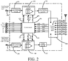
- FIG. 2 is a circuit diagram of a multimode power amplifier module according to an embodiment.
- the multimode power amplifier module shown in this embodiment is designed to work in GMS (Global System for Mobile Communication), EDGE (Enhanced Data Rate for GSM Evolution), TD_SCDMA (Time Division-Synchronous Code Division Multiple Access), and TDD_LTE (Time Division Long Term Evolution) modes.
- GMS Global System for Mobile Communication
- EDGE Enhanced Data Rate for GSM Evolution
- TD_SCDMA Time Division-Synchronous Code Division Multiple Access
- TDD_LTE Time Division Long Term Evolution
- an external pin of the multimode power amplifier module includes: 109 is a low-frequency input end of a low-frequency power amplifier channel and is used to access a low-frequency GSM/EDGE radio frequency signal.
- 110 is a power supply access end of a control power supply of a control circuit 104 and is used to access a control power supply Vbat.
- 111 is a TX_enble interface and is used to access an enable signal of TX to the control circuit.
- 113/114/115 are interfaces of logic signals B0/B1/B2 and are used to access the logic signals B0/B1/B2 to the control circuit.
- the three logic signals B0/B1/B2 and the enable signal of TX together constitute a working mode selection signal of the control circuit and together control the multimode power amplifier module to select the working modes.
- 112 is a baseband signal interface of the control circuit and is used to access a baseband signal Vramp.
- the baseband signal Vramp may be any value from 0 to 1.8 V.
- an output power of the multimode power amplifier module may be adjusted by setting different baseband signals Vramp.
- 116 is a high-frequency input end of the low-frequency power amplifier channel and is used to access GSM/EDGE/TD_SCDMA/TDD_LTE radio frequency signals.
- 117 is a transmit-receive switch and is located at an antenna end.
- 118/119/120/121/122/123 respectively corresponding to TRX1, TRX2, TRX3, TRX4, TRX5, and TRX6, are six transmit-receive ports, and may be used as transmission ports or output ports.
- the multimode power amplifier module includes: a low-frequency input matching network 101, used to access a low-frequency GSM/EDGE radio frequency signal, to implement matching of an impedance to 50 Ohm.
- the low-frequency power amplifier 102 is used to amplify the accessed low-frequency GSM/EDGE radio frequency signals (824 MHz to 849 MHz; 880 MHz to 915 MHz).
- the low-frequency output matching network 103 is used to implement low-frequency impedance conversion, to output a desired output power.
- the control circuit 104 may be implemented by using a CMOS. This is considered mainly from flexibility of design and costs.
- the control circuit 104 provides the amplifier control signal to the low-frequency power amplifier 103 and the high-frequency power amplifier 106 mainly according to the baseband signal Vramp and the working mode selection signal.
- the amplifier control signal includes: a logic signal Vmode, an offset signal Reg, and/or a collector voltage Vcc.
- the control circuit 104 also provides a power voltage and a logic voltage to the transmit-receive switch 108.
- the high-frequency input matching network 105 is used to access a high-frequency GSM/EDGE signal, a TD_SCDMA signal, and a TDD_LTE signal, to implement matching to 500 hm.
- the high-frequency power amplifier 106 amplifies the accessed high-frequency GSM/EDGE radio frequency signal, TD_SCDMA signal, and TDD_LTE signal (1710 MHz to 2025 MHz).
- the high-frequency output network 107 is used to implement high-frequency impedance conversion, to output a desired output power.
- the transmit-receive switch 108 is located at an antenna end and is connected to a transmit output and a receive input.
- the transmit-receive switch 108 in the embodiment shown in FIG. 2 is SP8T.
- the transmit-receive switch may be expanded to any SPXT according to needs, and is generally applied in a mobile phone antenna end. X is not less than 4. For example, three-mode five-frequency needs SP8T, five-mode 12-frequency needs SP16T, and SP10T, SP12T, or SP14T is applied in some cases.
- the control circuit in the multimode power amplifier module provides an amplifier control signal to the power amplifier according to the baseband signal Vramp and the working mode selection signal, to perform amplification adjustment by controlling the power amplifier.
- the multimode power amplifier module fully multiplexes the power amplifier channel in this manner, so that different working modes of high and low frequency bands can share the power amplifier channel through adjustment of the control circuit.
- the amplifier control signal herein includes: the logic signal Vmode, the offset signal Reg, and/or the collector voltage Vcc.
- control circuit performs amplification adjustment on the power amplifier by using the amplifier control signal is described in detail below by using several embodiments.
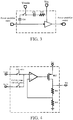
- FIG. 3 is a schematic diagram of controlling a power amplifier gain circuit according to a logic signal.
- the power amplifier shown in FIG. 3 may be a low-frequency power amplifier or may be a high-frequency power amplifier.
- a collector of the power amplifier is powered by the collector voltage Vcc output by the control circuit.
- a feedback circuit is disposed in the power amplifier.
- the feedback circuit of the power amplifier is composed of capacitors C30 and C31 and R31 that are mutually connected in series.
- the logic signal Vmode (for example, 0 or Vbat) output by the control circuit is used to control a feedback switch on the feedback circuit to be opened or closed.
- the logic signal Vmode controls the feedback switch to be opened, the feedback circuit is in a disconnected working state. In this case, because the feedback circuit does not function, the power amplifier is in a high gain mode. Generally, in a GSM working mode, a system requires the highest output power of the power amplifier module. Therefore, when the control circuit is in the working mode, the logic signal Vmode may be output to control the power amplifier to work in the high gain mode.
- the logic signal Vmode controls the feedback switch to be closed, the feedback circuit is in a connected working state. In this case, because the feedback circuit functions, the power amplifier is in a low gain mode.
- the logic signal Vmode may be output to control the power amplifier to work in the low gain mode.
- control circuit may determine, according to the working mode selection signal, a working mode in which the control circuit is, to determine whether the power amplifier should be located in the high gain mode or the low gain mode, to output a corresponding logic signal Vmode to the power amplifier.
- the collector voltage Vcc output by the control circuit is used to power the corresponding power amplifier as a collector voltage, to adjust an output power of the power amplifier. Therefore, the control circuit outputs different collector voltages Vcc according to current different working modes and may have a function of adjusting output of the power amplifier.
- FIG. 4 is a schematic diagram of a collector voltage generation circuit.
- the collector voltage generation circuit is located in the control circuit.
- the control circuit determines, according to the working mode selection signal, a working mode in which the control circuit is.
- a corresponding basis voltage is selected according to the working mode in which the control circuit is, to generate the collector voltage Vcc based on the basis voltage.
- an operational amplifier is disposed in the collector voltage generation circuit.
- An output end of the operational amplifier is connected to a gate of an insulated gate biopolar transistor.
- An emitter of the insulated gate biopolar transistor accesses the control power supply Vbat.
- a collector of the insulated gate biopolar transistor is an output end of the collector voltage Vcc and is used to output the collector voltage Vcc.
- a voltage R41 is provided between a negative input end of the operational amplifier and the output end of the collector voltage Vcc.
- a voltage R42 is provided between the negative input end of the operational amplifier and the ground.
- a positive input end of the operational amplifier is a basis voltage input end and is used to input a basis voltage selected by the control circuit. As shown in FIG. 4 , the basis voltage input end selects, by using different switches, to access different basis voltages.
- a GSM_enble switch in FIG. 4 When the working mode selection signal is in the GSM mode, a GSM_enble switch in FIG. 4 is closed, and the control circuit selects the baseband signal Vramp as the basis voltage, to generate the collector voltage Vcc.
- Vcc 1 + R 41 R 42 ⁇ Vramp .
- Different Vcc values are obtained from different baseband Vramp values.
- Vcc is a power supply voltage of the power amplifier collector, and the output power P and Vcc have the following correspondence: P ⁇ Vc c 2 2 R L , where RL is a load of the power amplifier and is determined by the output matching network. Therefore, the control circuit may adjust the output power of the power amplifier by using different baseband signals Vramp.
- Vcc 1 + R 41 R 42 ⁇ Vref .
- Vref4 is generated by a circuit principle diagram in FIG. 5 .
- Vref V BEQ 53 + R 52 R 51 ⁇ V T ⁇ lnn .
- V BE53 is a voltage difference from a base to an emitter of a biopolar transistor Q53, and is generally 0.7 V in a silicon process, n is a ratio of Q52 and Q51 emitter areas, and V T is a thermal voltage and is 0.026 V.
- the offset signal Reg is used to adjust a current of the power amplifier.
- the control circuit controls, according to the working mode selection signal, to close a corresponding switch in the offset signal switch group, to generate an offset signal Reg corresponding to the working mode. Switches corresponding to the working modes are disposed in the offset signal switch group.
- the offset signal may be a voltage signal or may be a current signal.
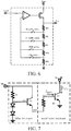
- FIG. 6 is a schematic diagram of an offset signal generation circuit.
- the offset signal generation circuit is located in the control circuit.
- the control circuit determines, according to the working mode selection signal, a working mode in which the control circuit is.
- the control circuit controls, according to the working mode in which the control circuit is, to close a corresponding switch in the offset signal switch group, to generate an offset signal Reg corresponding to the working mode.
- the offset signal generation circuit includes: an operational amplifier, a PMOS tube, and the offset signal switch group.
- a positive input end of the operational amplifier accesses the reference voltage Vref, and the reference voltage Vref is determined according to the offset signal Reg. Different offset signals Reg are needed in different modes. Reg and Vref conform to certain formulas.
- An output end of the operational amplifier is connected to a gate of the PMOS tube.
- a source of the PMOS accesses the control power supply Vbat.
- a drain of the PMOS is an output end of the offset signal generation circuit and is used to output the offset signal Reg.
- the reference voltage Vref is generated based on the circuit shown in FIG. 5 and is not described in detail herein.
- the offset signal switch group is connected between a negative input end of the operational amplifier and a collector of the PMOS tube. Resistors are connected in series between the switches in the offset signal switch group.
- a TDD_SCDMA_enble switch, a TDD_LTE_enble switch, an EDGE_enble switch, and a GSM_enble switch are disposed in the offset signal switch group.
- resistors R61, R62, R63, R64, and R65 are respectively connected in series between the switches.
- the control circuit determines, according to the working mode selection signal, a working mode in which the control circuit is.
- the control circuit selects, according to the working mode in which the control circuit is, to control closing a corresponding switch in the offset signal switch group. For example, when in the TDD_LTE mode, the control circuit selects to close the TDD_LTE_enble switch, and other switches remain in a disconnected state.
- the offset signal Reg is generated based on this.
- the offset signal Reg is higher, and in the EDGE/TD_SCDMA modes, the offset signals Reg are sequentially reduced.
- the offset voltage in the TDD_LTE mode is between that in the GSM mode and those in the EDGE/TD_SCDMA modes and mainly balances power consumption and linearity.
- FIG. 7 is a principle diagram of controlling a one-stage circuit in a power amplifier by an offset signal.
- the power amplifier may be two-stage or three-stage, and each stage may be controlled by using an offset circuit part in FIG. 7 .
- V 71 ⁇ R D 1 + R D 3 R D 1 + R D 2 + R 71 ⁇ Reg V 71 ⁇ R D 1 + R D 3 R D 1 + R D 2 + R 71 ⁇ Reg , where R D1 and R D2 are conduction resistors of diodes D1 and D2, and after the diodes D1 and D2 are selected, R D1 and R D2 are fixed values.
- V 72 V 71 - V BEQ71
- V 73 V BEQ72
- I BQ 72 V 72 ⁇ V 73 R 72
- I CQ 72 ⁇ ⁇ I bQ 72 ⁇ ⁇ ⁇ R D 1 + R D 2 R D 1 + R D 2 + R 72 ⁇ Reg ⁇ V BEQ 72 ⁇ V BEQ 72 R 71
- V BEQ71 and V BEQ72 are voltage differences between bases and emitters of heterojunction biopolar transistors (HBT) Q71 and Q72.
- HBT heterojunction biopolar transistors
- V be 1.3 V.
- I BQ72 is a base current of the heterojunction biopolar transistor Q72
- ⁇ is an amplification multiple, generally ranges from 60 to 160, and is mainly determined by a process of the heterojunction biopolar transistor.
- the offset signal Reg accesses the offset circuit of the power amplifier.
- the offset circuit includes R71, D71, D72, and a collector of a biopolar transistor Q71.
- the diodes D71 and D72 and R71 generate V71 through voltage division.
- V71 generates V72 through voltage drop of one V BE .
- a voltage difference between V72 and V73 determines a current passing through R72, that is, a base current of the biopolar transistor Q72, to implement current control over Q72.
- Q72 herein is the power amplifier tube of the power amplifier.
- the collector of Q71 may also be directly connected to Vbat.
- the power amplifier should be in a linear power amplification state all the time.
- the control circuit needs to provide a relatively large offset signal Reg.
- the power amplifier needs only a relatively low offset current to implement enough linearity.
- the control circuit provides a relatively small offset signal Reg, the offset current needed by the power amplifier can be reduced, to reduce power consumption of the multimode power amplifier module.
- the control circuit in the multimode power amplifier module provides the amplifier control signal to the power amplifier according to the baseband signal and the working mode selection signal, to perform amplification adjustment by controlling the power amplifier.
- the amplifier control signal herein includes but is not limited to: the logic signal Vmode, the offset signal Reg, and/or the collector voltage Vcc.
- the baseband signal Vramp participate in selection of the two time-division multiplexing modes as a logic level, and may be a high level or a low level. Therefore, the offset voltage or offset current in the two time-division multiplexing modes has only one value and cannot be adjusted according to the output power of the multimode power amplifier module.
- offset voltage and offset current are collectively referred to as offset signals Reg. that is, in a scenario in which a voltage signal needs to be used as an offset signal, the offset signal Reg is the offset voltage; in a scenario in which a current signal needs to be used as an offset signal, the offset signal Reg is the offset current.
- Change of the offset voltage or offset current causes an output current of the power amplifier to change, to optimize performance and power consumption of the entire multimode power amplifier module.
- control circuit adjusts the offset signal Reg of the power amplifier by using the baseband signal Vramp is specifically described below by using several other embodiments.
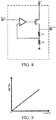
- FIG. 8 is a schematic diagram of a first embodiment of controlling a power amplifier offset signal according to a baseband signal.
- the baseband signal Vramp is input into the negative input end (also referred to as a reverse-phase input end) of the operational amplifier.
- the output end of the operational amplifier is connected to a gate of an insulated gate biopolar transistor.
- a source of the insulated gate biopolar transistor accesses the control power supply Vbat.
- a drain of the insulated gate biopolar transistor is an output end of the offset signal Reg and is used to output an offset signal.
- the drain of the insulated gate biopolar transistor is grounded by using resistors R21 and R22.
- a connection point of the resistors R21 and R22 is directly connected to a positive input end (also referred to as an in-phase input end) of the operational amplifier.
- the offset signal Reg As shown in FIG. 9 , in the two time-division multiplexing modes, TD_SCDMA and TDD_LTE, by using the baseband signal Vramp, the offset signal Reg and the baseband signal Vramp are made to satisfy a linear function relationship.
- the offset signal Reg herein may be a voltage signal or may be a current signal.
- the corresponding parameter G can be obtained.
- the following formula: Reg _ HB 1 + R 21 R 22 ⁇ Vramp can be obtained.
- the parameter G needed by a user can be obtained by selecting proper resistances of the resistors R21 and R22.
- FIG. 10 is a schematic diagram of a second embodiment of controlling a power amplifier offset signal according to a baseband signal.
- connection manners of most of circuits are basically the same as those in the first embodiment, and a difference mainly lies in a drain output part of the insulated gate biopolar transistor.
- the collector of the insulated gate biopolar transistor is connected to the ground by using the resistors R31, R32, R33, and R34.
- a gating switch is disposed between a connection point of the resistors R31 and R32 and the positive input end of the operational amplifier. The gating switch is conducted when Vramp ⁇ A and is closed in other cases.
- a gating switch is disposed between a connection point of the resistors R32 and R33 and the positive input end of the operational amplifier. The gating switch is conducted when A ⁇ Vramp ⁇ B and is closed in other cases.
- a gating switch is disposed between a connection point of the resistors R33 and R34 and the positive input end of the operational amplifier. The gating switch is conducted when Vramp>B and is closed in other cases.
- a and B are particular threshold voltages.
- the offset signal Reg and the baseband signal Vramp may be made to in the stair step linear relationship shown in FIG. 11 .
- a value of a relationship between VI, V2, and V3 is determined by the designed performance requirement, and the value may be 0.
- FIG. 12 is a schematic diagram of a third embodiment of controlling a power amplifier offset signal according to a baseband signal.
- connection manners of most of circuits are basically the same as those in the second embodiment, and a difference mainly lies in that the baseband signal Vramp and the reference voltage Vref41 respectively access a positive input end and a negative input end of a multi-channel analog switch (MUX).
- An output end signal Vref42 of the multi-channel analog switch in replacement of an original baseband signal Vramp, accesses the negative input end of the operational amplifier.
- the multi-channel analog switch has at least two channels, and opening or closing of the channels are determined by the baseband signal and the working mode.
- the collector of the insulated gate biopolar transistor is connected to the ground by using the resistors R41, R42, R43, and R44.
- a gating switch is disposed between a connection point of the resistors R41 and R42 and the positive input end of the operational amplifier. The gating switch is conducted when Vramp ⁇ A and is closed in other cases.
- a gating switch is disposed between a connection point of the resistors R42 and R43 and the positive input end of the operational amplifier. The gating switch is conducted when A ⁇ Vramp ⁇ B and is closed in other cases.
- a gating switch is disposed between a connection point of the resistors R43 and R44 and the positive input end of the operational amplifier. The gating switch is conducted when Vramp>B and is closed in other cases.
- a and B are particular threshold voltages.
- the offset signal Reg and the baseband signal Vramp may be made to in the step linear relationship shown in FIG. 13 .
- the transistor herein includes but is not limited to the insulated gate biopolar transistor, the field-effect transistor, or a triode.
- Corresponding circuit adjustment is a conventional technical means that can be mastered by a person skilled in the art and does not go beyond the technical teaching provided in the present invention, and is not described in detail herein.
- TD_SCDMA and TDD_LTE are both time-division multiplexing working modes, they have different requirements on the offset signal Reg. therefore, in the TD SCDMA and TDD_LTE modes, working performance can be further optimized by setting different baseband signals Vramp.
- a multimode power amplifier module output control method provided in the present invention may be further summarized.
- the method includes the following steps: providing an offset signal to a low-frequency power amplifier channel, where a magnitude of the offset signal is determined by a magnitude of a baseband signal and a working mode; and providing an offset signal to a high-frequency power amplifier channel, where a magnitude of the offset signal is determined by the magnitude of the baseband signal and the working mode.
- the offset signal is controlled by the baseband signal and the working mode and linearly or very nearly linearly changes with the baseband signal.
- the offset signal is controlled by the baseband signal and the working mode and changes with the baseband signal in a stair step manner.
- the offset signal is controlled by the baseband signal and the working mode and linearly changes with the baseband signal in a step manner.
- the multimode power amplifier module shown in the foregoing embodiment may be used in a chip.
- the structure of the multimode power amplifier module in the chip is not described in detail herein.
- the multimode power amplifier module may also be used in a communication terminal as an important component of a radio frequency circuit.
- the communication terminal herein refers to a computer device that may be used in a mobile environment and supports a plurality of communication modes such as GSM, EDGE, TD_SCDMA, TDD_LTE, and FDD_LTE.
- the communication terminal includes but is not limited to a mobile phone, a notebook computer, a tablet computer, and an on-board computer.
- the multimode power amplifier module is also applicable to scenarios to which other multi-mode technologies are applied, for example, a communication base station compatible with multiple communication systems. Details are not provided herein.
Landscapes
- Engineering & Computer Science (AREA)
- Power Engineering (AREA)
- Microelectronics & Electronic Packaging (AREA)
- Physics & Mathematics (AREA)
- Nonlinear Science (AREA)
- Computer Networks & Wireless Communication (AREA)
- Signal Processing (AREA)
- Amplifiers (AREA)
Priority Applications (1)
| Application Number | Priority Date | Filing Date | Title |
|---|---|---|---|
| EP23206865.0A EP4293900A3 (de) | 2015-12-01 | 2016-12-01 | Multimodales leistungsverstärkermodul, chip und kommunikationsendgerät |
Applications Claiming Priority (3)
| Application Number | Priority Date | Filing Date | Title |
|---|---|---|---|
| CN201510870113.1A CN106803747B (zh) | 2015-12-01 | 2015-12-01 | 多模功率放大器模组、芯片及通信终端 |
| CN201610517854.6A CN106208983B (zh) | 2016-06-30 | 2016-06-30 | 面向时分复用的多模功率放大器模组、芯片及通信终端 |
| PCT/CN2016/108305 WO2017092705A1 (zh) | 2015-12-01 | 2016-12-01 | 多模功率放大器模组、芯片及通信终端 |
Related Child Applications (1)
| Application Number | Title | Priority Date | Filing Date |
|---|---|---|---|
| EP23206865.0A Division EP4293900A3 (de) | 2015-12-01 | 2016-12-01 | Multimodales leistungsverstärkermodul, chip und kommunikationsendgerät |
Publications (2)
| Publication Number | Publication Date |
|---|---|
| EP3386101A1 true EP3386101A1 (de) | 2018-10-10 |
| EP3386101A4 EP3386101A4 (de) | 2019-07-03 |
Family
ID=58796338
Family Applications (2)
| Application Number | Title | Priority Date | Filing Date |
|---|---|---|---|
| EP23206865.0A Pending EP4293900A3 (de) | 2015-12-01 | 2016-12-01 | Multimodales leistungsverstärkermodul, chip und kommunikationsendgerät |
| EP16870015.1A Ceased EP3386101A4 (de) | 2015-12-01 | 2016-12-01 | Multimodales leistungsverstärkermodul, chip und kommunikationsendgerät |
Family Applications Before (1)
| Application Number | Title | Priority Date | Filing Date |
|---|---|---|---|
| EP23206865.0A Pending EP4293900A3 (de) | 2015-12-01 | 2016-12-01 | Multimodales leistungsverstärkermodul, chip und kommunikationsendgerät |
Country Status (3)
| Country | Link |
|---|---|
| US (1) | US10637407B2 (de) |
| EP (2) | EP4293900A3 (de) |
| WO (1) | WO2017092705A1 (de) |
Families Citing this family (13)
| Publication number | Priority date | Publication date | Assignee | Title |
|---|---|---|---|---|
| CN110266280B (zh) * | 2019-06-13 | 2023-06-30 | 上海华虹宏力半导体制造有限公司 | 三电压供电功率放大器电路、装置及半导体集成电路 |
| CN110311635B (zh) * | 2019-06-28 | 2024-10-29 | 京信网络系统股份有限公司 | 超宽带放大器和基于该放大器的多载波发射、收发装置 |
| CN110311693A (zh) * | 2019-08-01 | 2019-10-08 | 江西联智集成电路有限公司 | 一种功率放大器芯片及无线电发射器 |
| CN111294214B (zh) * | 2020-01-21 | 2021-09-14 | Oppo广东移动通信有限公司 | 供电方法及相关产品 |
| CN111313853B (zh) * | 2020-04-09 | 2023-07-21 | 西安芯辉光电科技有限公司 | 一种双模式多通道跨阻放大器 |
| CN113676193B (zh) * | 2021-08-12 | 2022-11-11 | Oppo广东移动通信有限公司 | 发射模组、射频系统及通信设备 |
| CN116416889B (zh) * | 2021-12-31 | 2025-12-23 | 格科微电子(上海)有限公司 | 改善面板显示效果的方法及装置、芯片 |
| CN115277930B (zh) * | 2022-06-14 | 2024-04-26 | 维沃移动通信有限公司 | 供电方法、装置及电子设备 |
| CN115149912A (zh) * | 2022-07-20 | 2022-10-04 | 普源精电科技股份有限公司 | 模拟前端芯片、模拟前端电路及信号处理装置 |
| CN114978074B (zh) * | 2022-07-25 | 2022-11-11 | 成都嘉纳海威科技有限责任公司 | 一种三通道收发放大芯片 |
| CN115425993B (zh) * | 2022-09-01 | 2024-08-02 | Oppo广东移动通信有限公司 | 多模多频功率放大器件、切换方法、射频前端装置和设备 |
| US20240223227A1 (en) * | 2022-12-28 | 2024-07-04 | Skyworks Solutions, Inc. | Consolidation of amplifier ramping for 2g and 5g transmission |
| CN119674487B (zh) * | 2024-11-01 | 2025-11-14 | 广州致远仪器有限公司 | 定向耦合器电路、线路板及射频测量设备 |
Family Cites Families (13)
| Publication number | Priority date | Publication date | Assignee | Title |
|---|---|---|---|---|
| JP2006261714A (ja) * | 2005-03-15 | 2006-09-28 | Renesas Technology Corp | 通信用半導体集積回路および携帯通信端末 |
| JP4683468B2 (ja) * | 2005-03-22 | 2011-05-18 | ルネサスエレクトロニクス株式会社 | 高周波電力増幅回路 |
| JP4614238B2 (ja) * | 2006-07-14 | 2011-01-19 | ルネサスエレクトロニクス株式会社 | Rf電力増幅装置 |
| US8718582B2 (en) * | 2008-02-08 | 2014-05-06 | Qualcomm Incorporated | Multi-mode power amplifiers |
| CN101667810B (zh) * | 2009-09-29 | 2011-11-16 | 锐迪科科技有限公司 | 双频射频功率放大器电路芯片 |
| CN102055491B (zh) * | 2010-04-14 | 2015-11-25 | 锐迪科创微电子(北京)有限公司 | 射频前端模块及具有该模块的移动通信装置 |
| KR101675342B1 (ko) * | 2010-06-01 | 2016-11-11 | 삼성전자주식회사 | 휴대용 단말기의 전력 증폭 장치 및 방법 |
| CN101902243B (zh) * | 2010-07-28 | 2013-01-02 | 锐迪科创微电子(北京)有限公司 | 可配置多模式射频前端模块及具有该模块的移动终端 |
| CN102404022A (zh) * | 2011-11-04 | 2012-04-04 | 中兴通讯股份有限公司 | 功率放大模块、射频前端模块和多模终端 |
| CN102510297A (zh) * | 2011-11-04 | 2012-06-20 | 中兴通讯股份有限公司 | 功率放大模块、多模射频收发器、双工器和多模终端 |
| CN103633949B (zh) * | 2012-08-21 | 2020-04-03 | 唯捷创芯(天津)电子技术股份有限公司 | 多模功率放大器、多模切换方法及其移动终端 |
| JP5958774B2 (ja) * | 2014-02-04 | 2016-08-02 | 株式会社村田製作所 | 電力増幅モジュール |
| CN104485907A (zh) * | 2015-01-03 | 2015-04-01 | 广州钧衡微电子科技有限公司 | 一种高效率多模射频功率放大器 |
-
2016
- 2016-12-01 WO PCT/CN2016/108305 patent/WO2017092705A1/zh not_active Ceased
- 2016-12-01 EP EP23206865.0A patent/EP4293900A3/de active Pending
- 2016-12-01 EP EP16870015.1A patent/EP3386101A4/de not_active Ceased
- 2016-12-01 US US15/780,241 patent/US10637407B2/en active Active
Also Published As
| Publication number | Publication date |
|---|---|
| US10637407B2 (en) | 2020-04-28 |
| EP4293900A3 (de) | 2024-03-27 |
| EP4293900A2 (de) | 2023-12-20 |
| WO2017092705A1 (zh) | 2017-06-08 |
| EP3386101A4 (de) | 2019-07-03 |
| US20180375479A1 (en) | 2018-12-27 |
Similar Documents
| Publication | Publication Date | Title |
|---|---|---|
| EP3386101A1 (de) | Multimodales leistungsverstärkermodul, chip und kommunikationsendgerät | |
| CN106208983B (zh) | 面向时分复用的多模功率放大器模组、芯片及通信终端 | |
| CN103633949B (zh) | 多模功率放大器、多模切换方法及其移动终端 | |
| EP3163746B1 (de) | Leistungsverstärker, fernfunkeinheit und basisstation | |
| CN106803747B (zh) | 多模功率放大器模组、芯片及通信终端 | |
| US8421539B2 (en) | Multi-mode high efficiency linear power amplifier | |
| CN105490648B (zh) | 一种多模功率放大器及其移动终端 | |
| CN104917475B (zh) | 一种可调增益功率放大器、增益调节方法及移动终端 | |
| US7876157B1 (en) | Power amplifier bias circuit having controllable current profile | |
| US20100134189A1 (en) | Radio frequency amplifier circuit and mobile communication terminal using the same | |
| WO2018001380A1 (zh) | 多增益模式功率放大器、芯片及通信终端 | |
| WO2017220027A1 (zh) | 射频前端发射方法及发射模块、芯片和通信终端 | |
| CN118449545B (zh) | 射频开关、射频前端模块、射频前端芯片及终端设备 | |
| KR20150035219A (ko) | 고주파 스위치 | |
| CN104980384A (zh) | Dpd mcpa的信号处理方法、系统、装置及mcpa设备 | |
| US11190150B2 (en) | CMOS triple-band RF VGA and power amplifier in linear transmitter | |
| US20200389342A1 (en) | Transmitters and methods for operating the same | |
| US8324967B2 (en) | System and method for controlling a power amplifier using a programmable ramp circuit | |
| WO2023045262A1 (zh) | 功率放大装置和发射机 | |
| US9270305B2 (en) | Method and system for multi-mode signal transmission | |
| CN106559044A (zh) | 一种应用于多模多频mmmb射频功放的数字预失真线性化的系统 |
Legal Events
| Date | Code | Title | Description |
|---|---|---|---|
| STAA | Information on the status of an ep patent application or granted ep patent |
Free format text: STATUS: THE INTERNATIONAL PUBLICATION HAS BEEN MADE |
|
| PUAI | Public reference made under article 153(3) epc to a published international application that has entered the european phase |
Free format text: ORIGINAL CODE: 0009012 |
|
| STAA | Information on the status of an ep patent application or granted ep patent |
Free format text: STATUS: REQUEST FOR EXAMINATION WAS MADE |
|
| 17P | Request for examination filed |
Effective date: 20180702 |
|
| AK | Designated contracting states |
Kind code of ref document: A1 Designated state(s): AL AT BE BG CH CY CZ DE DK EE ES FI FR GB GR HR HU IE IS IT LI LT LU LV MC MK MT NL NO PL PT RO RS SE SI SK SM TR |
|
| AX | Request for extension of the european patent |
Extension state: BA ME |
|
| DAV | Request for validation of the european patent (deleted) | ||
| DAX | Request for extension of the european patent (deleted) | ||
| A4 | Supplementary search report drawn up and despatched |
Effective date: 20190604 |
|
| RIC1 | Information provided on ipc code assigned before grant |
Ipc: H03F 1/42 20060101AFI20190528BHEP |
|
| STAA | Information on the status of an ep patent application or granted ep patent |
Free format text: STATUS: EXAMINATION IS IN PROGRESS |
|
| 17Q | First examination report despatched |
Effective date: 20210803 |
|
| REG | Reference to a national code |
Ref country code: DE Ref legal event code: R003 |
|
| STAA | Information on the status of an ep patent application or granted ep patent |
Free format text: STATUS: THE APPLICATION HAS BEEN REFUSED |
|
| 18R | Application refused |
Effective date: 20230907 |