EP3386104A1 - Kalibrierung eines taktzyklus und frequenzverdopplungsschaltung - Google Patents
Kalibrierung eines taktzyklus und frequenzverdopplungsschaltung Download PDFInfo
- Publication number
- EP3386104A1 EP3386104A1 EP16894185.4A EP16894185A EP3386104A1 EP 3386104 A1 EP3386104 A1 EP 3386104A1 EP 16894185 A EP16894185 A EP 16894185A EP 3386104 A1 EP3386104 A1 EP 3386104A1
- Authority
- EP
- European Patent Office
- Prior art keywords
- clock signal
- delay unit
- clock
- duty cycle
- delay
- Prior art date
- Legal status (The legal status is an assumption and is not a legal conclusion. Google has not performed a legal analysis and makes no representation as to the accuracy of the status listed.)
- Granted
Links
- 238000001514 detection method Methods 0.000 claims abstract description 16
- 230000000630 rising effect Effects 0.000 claims description 32
- 230000001960 triggered effect Effects 0.000 claims description 17
- 230000003111 delayed effect Effects 0.000 claims description 11
- 238000012545 processing Methods 0.000 claims description 6
- 238000010586 diagram Methods 0.000 description 11
- 238000013461 design Methods 0.000 description 9
- 238000000034 method Methods 0.000 description 4
- 238000000926 separation method Methods 0.000 description 4
- 238000005516 engineering process Methods 0.000 description 3
- 238000012986 modification Methods 0.000 description 2
- 230000004048 modification Effects 0.000 description 2
- 230000001010 compromised effect Effects 0.000 description 1
- 230000007274 generation of a signal involved in cell-cell signaling Effects 0.000 description 1
- 238000013139 quantization Methods 0.000 description 1
Images


Classifications
-
- H—ELECTRICITY
- H03—ELECTRONIC CIRCUITRY
- H03K—PULSE TECHNIQUE
- H03K3/00—Circuits for generating electric pulses; Monostable, bistable or multistable circuits
- H03K3/01—Details
- H03K3/017—Adjustment of width or dutycycle of pulses
-
- H—ELECTRICITY
- H03—ELECTRONIC CIRCUITRY
- H03K—PULSE TECHNIQUE
- H03K5/00—Manipulating of pulses not covered by one of the other main groups of this subclass
- H03K5/156—Arrangements in which a continuous pulse train is transformed into a train having a desired pattern
- H03K5/1565—Arrangements in which a continuous pulse train is transformed into a train having a desired pattern the output pulses having a constant duty cycle
-
- H—ELECTRICITY
- H03—ELECTRONIC CIRCUITRY
- H03K—PULSE TECHNIQUE
- H03K5/00—Manipulating of pulses not covered by one of the other main groups of this subclass
- H03K5/00006—Changing the frequency
-
- H—ELECTRICITY
- H03—ELECTRONIC CIRCUITRY
- H03L—AUTOMATIC CONTROL, STARTING, SYNCHRONISATION OR STABILISATION OF GENERATORS OF ELECTRONIC OSCILLATIONS OR PULSES
- H03L7/00—Automatic control of frequency or phase; Synchronisation
- H03L7/06—Automatic control of frequency or phase; Synchronisation using a reference signal applied to a frequency- or phase-locked loop
- H03L7/08—Details of the phase-locked loop
- H03L7/085—Details of the phase-locked loop concerning mainly the frequency- or phase-detection arrangement including the filtering or amplification of its output signal
-
- H—ELECTRICITY
- H03—ELECTRONIC CIRCUITRY
- H03K—PULSE TECHNIQUE
- H03K19/00—Logic circuits, i.e. having at least two inputs acting on one output; Inverting circuits
- H03K19/20—Logic circuits, i.e. having at least two inputs acting on one output; Inverting circuits characterised by logic function, e.g. AND, OR, NOR, NOT circuits
Definitions
- the present invention relates to the field of integrated circuit technologies, and more particularly to a clock duty cycle calibration and frequency multiplier circuit used in a square wave frequency multiplier.
- a clock signal frequency multiplication technology is required for reducing multiples of frequency multiplication of a phase-locked loop.
- the clock signal frequency multiplication technology may be implemented in a manner of an analog circuit and a digital circuit.
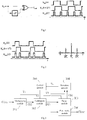
- FIG. 1 shows a method of implementing clock signal frequency multiplication through a digital circuit.
- An exclusive-OR operation is performed on an input clock signal Vin and a clock signal obtained after the Vin being delayed by ⁇ T, to obtain a frequency multiplication output clock signal Vout.
- a duty cycle of an input clock signal is in a range of 40% to 60%.
- Implementing clock signal frequency multiplication through a digital circuit requires that the duty cycle of the input clock signal is close to 50% as much as possible, otherwise the output clock signal will include an additional spurious component.
- the duty cycle of the input clock signal deviates from 50%.
- the output clock signal not only includes double frequency component of the input clock signal, but also includes single and triple frequency component. This deteriorates purity of the output clock signal of a phase-lock loop.
- An objective of the present invention is to provide a clock duty cycle calibration and frequency multiplier circuit, so as to implement high-precision clock signal frequency multiplication with relatively low circuit complexity and low cost.
- the present invention provides a clock duty cycle calibration and frequency multiplier circuit, including:
- the calibration module includes a first delay unit, a second delay unit, and a gate circuit, the first delay unit and the second delay unit are connected in parallel, then connected to the gate circuit, and the first delay unit and the second delay unit are identical adjustable delay units.
- the gate circuit is an AND gate circuit or an OR gate circuit.
- the delay module includes:
- the detection module includes: a first edge-triggered flip-flop, configured to compare whether a phase difference between the third clock signal CK3 and the fourth clock signal CK4 is 360°, and output a comparison result as a feedback signal.
- a first edge-triggered flip-flop configured to compare whether a phase difference between the third clock signal CK3 and the fourth clock signal CK4 is 360°, and output a comparison result as a feedback signal.
- a third delay unit and a fourth delay unit are adjusted of a same delay value.
- the detection module further includes: a second edge-triggered flip-flop, configured to compare whether rising edges of square waves of the third clock signal CK3 and a clock signal obtained after the third clock signal CK3 being delayed by a third delay unit are aligned with falling edges, and output a comparison result as a feedback signal.
- a second edge-triggered flip-flop configured to compare whether rising edges of square waves of the third clock signal CK3 and a clock signal obtained after the third clock signal CK3 being delayed by a third delay unit are aligned with falling edges, and output a comparison result as a feedback signal.
- the multiplexing module enables the first clock signal CKin to reversely pass; and the preset value is a feedback signal value of the second edge-triggered flip-flop when a duty cycle of the first clock signal CKin conforms to an operational rule of a gate circuit of the calibration module.
- a delay value of the first delay unit or the second delay unit is adjusted.
- the frequency multiplication module includes:
- a clock duty cycle calibration and frequency multiplier circuit of the present invention implements separation of a frequency multiplication delay unit and a calibration delay unit, and simplifies circuit design.
- the calibration delay unit demands a large dynamic range and a small adjustment of step precision and have no requirement for phase noise performance; and the frequency multiplication delay unit may be fixed delay, and requires only low phase noise design. In this way, optimal design of different circuit modules can be implemented, and power consumption and area consumption are reduced.
- a clock duty cycle calibration and frequency multiplier circuit is used to perform delay, comparison, and a logic operation on a clock signal, so as to implement high-precision clock signal frequency multiplication with relatively low circuit complexity and low cost.
- the clock duty cycle calibration and frequency multiplier circuit includes a multiplexing module 301, a calibration module 302, a delay module 303, a detection module 304, a control module 305, and a frequency multiplication module 306.
- the multiplexing module 301 inverts an input first clock signal CKin based on a first control signal V1, then outputs a second clock signal CK2 to the calibration module 302 .
- the multiplexing module 301 may use a multiplexer.
- the calibration module calibration module 302 adjusts a duty cycle of the second clock signal CK2 based on a second control signal V2, and finally outputs a third clock signal CK3 with a 50% duty cycle to the delay module 303, the detection module 304, and the frequency multiplication module 306.
- the calibration module 302 includes a differential phase adjustment circuit and a gate circuit.
- the differential phase adjustment circuit includes two identical adjustable delay units.
- the delay module 303 performs a delay operation on the third clock signal CK3 based on a third control signal V3, then outputs a fourth clock signal CK4 to the detection module 304.
- the delay module 303 includes two identical adjustable delay units.
- the detection module 304 compares the third clock signal CK3 and the fourth clock signal CK4 that are input thereto, and outputs a feedback signal Va, based on a comparison result, to the control module 305.
- the detection module 304 includes two edge-triggered flip-flops.
- the control module 305 outputs the first control signal V1, the second control signal V2, and the third control signal V3 based on the input feedback signal Va.
- the control module 305 may control the delay unit and the multiplexer by using the feedback signal of the edge-triggered flip-flop. Specifically, how to control the delay unit and the multiplexer is a prior art, and therefore details are not described herein.
- the detection module 304 includes two edge-triggered flip-flops.
- One edge-triggered flip-flop is configured to detect whether rising edges of square waves of the input third clock signal CK3 and the output fourth clock signal CK4 of the delay module 304 are aligned, that is, whether a phase difference between input and output clock signals is 360°.
- the control module 305 performs adjustment operations of same delay values on these two delay units of the delay module 303 based on a detection result, to enable the phase difference between the input and the output clock signals to be 360°.
- the other edge-triggered flip-flop is configured to detect whether rising edges of square waves of the input third clock signal CK3 of the delay module 304 and an output clock signal of a delay unit at an input end of the delay module 304 are aligned with falling edges.
- the control module 305 firstly determines, based on a feedback signal of the edge-triggered flip-flop and a gate circuit used by the calibration module 302 in this case, whether to control the multiplexing module 301 to invert the first clock signal CKin, and then adjusts a delay value to a delay unit of the calibration module 302.
- a duty cycle of the third clock signal CK3 is 50%.
- the frequency multiplication module 306 performs a frequency multiplication operation on the third clock signal CK3, and outputs a fifth clock signal CKout.
- the frequency multiplication module 306 includes a fixed delay unit and an exclusive-OR gate circuit.
- FIG. 4 and FIG. 5 are a schematic diagram of a circuit structure of an embodiment of a clock duty cycle calibration and frequency multiplier circuit according to the present invention, and a timing diagram of a clock signal status in a calibration process, respectively.
- the multiplexing module in this embodiment includes a multiplexer MUX; calibration module includes a differential phase adjustment circuit that includes two identical adjustable delay units DL1 and DL2, and an AND gate circuit; the delay module includes two identical adjustable delay units DL3 and DL4 connected in series; detection module includes two rising edge D flip-flops generating outputs call and cal2, wherein a first flip-flop outputting call is configured to detect whether rising edges of square waves of clock signals at node A and node C at a same timing are aligned, a second flip-flop generating cal2 is configured to detect whether a rising edge of a square wave of a clock signal at node B is aligned with a falling edge of a square wave of a clock signal at node A at a same timing, and these two flip-flops feed back detection results to the control module; frequency multiplication module includes a fixed delay unit DL5 and an exclusive-OR gate circuit.
- a calibration and frequency multiplication process in this embodiment will be described in detail with reference to FIG. 5 .
- the delay units DL1 and DL2 are firstly adjusted to a same delay value. In this way, after a clock signal is input, a duty cycle of a clock signal at node A is consistent with that of the input clock signal, thereby avoiding a technical requirement of approximately zero delay when only a single delay unit is used and avoiding a technical requirement on dynamic ranges of the two delay units DL1 and DL2 if used.
- the fixed delay unit DL5 is set to be a delay value based on a multiplication value needed.
- a clock signal is input.
- the duty cycle value of the input clock signal does not affect implementation of the present invention.
- a square wave of a clock signal with a duty cycle greater than 50% is used for description.
- a waveform diagram of clock signals at three nodes A, B and C in the circuit is shown in 1 in step 1.
- a rising edge of a square wave of a clock signal at node C is needed to be aligned with a rising edge of a square wave of a clock signal at node A. That is, a phase difference between clock signals at nodes A and C is adjusted to 360°.
- the clock signals at two nodes A and C are input to the rising edge D flip-flop call simultaneously.
- control module controls the delay units DL3 and DL4 to keep the delay values at this time based on the change of the feedback signal output by the rising edge D flip-flop call.
- the phase difference between the clock signals at nodes A and C is 360°.
- the control module does not respond to a feedback signal of the rising edge D flip-flop cal2.
- the control module starts to respond to the feedback signal of the rising edge D flip-flop cal2.
- the calibration module uses an AND gate circuit to perform clock signal duty cycle calibration. Therefore, the duty cycle of the clock signal input into the calibration module is needed to be greater than 50% so that a clock signal with a 50% duty cycle can be obtained by using an operation of the AND gate.
- the delay units DL1 and DL2 are set to be same delay values.
- the control module controls the multiplexer MUX to enable the input clock signal to pass directly.
- the operation can ensure the duty cycle of the clock signal at node A to be greater than 50%. That is, the clock signal duty cycle input into the calibration module is greater than 50%.
- the waveform diagram of the clock signals at three nodes A, B and C in the circuit is shown in 3 in step 2.
- the delay units DL1 and DL2 perform delay operations on the clock signals based on the input control signal.
- An AND operation is performed on the clock signals that has been delayed by the delay units DL1 and DL2, to gradually decrease duty cycle. Because the phase difference between the clock signals at two nodes A and B is 180°, the rising edge of the square wave of the clock signal at node B is gradually aligned with the falling edge of the square wave of the clock signal at node A as the duty cycles decrease.
- the control module controls the delay units DL1 and DL2 to keep delay values at this time based on the change of the feedback signal output by the rising edge D flip-flop cal2. Because the phase difference between the clock signals at the nodes A and B is 180°, clock signals of a 50% duty cycles are obtained at three nodes A, B and C.
- the operating principle of a flip-flop is of a successive approximation type. That is, when the edges of two nodes are close to an extent, the flip-flop flips. Close/ approximation precision is determined by the property of an used flip-flop and delay unit, and this also determines the precision of a clock signal duty cycle finally obtained.
- the clock signals input to the control ends of a rising edge flip-flop may be exchanged, and the edge-triggered flip-flop configured to detect aligning of edges of two nodes A and B may also use a falling edge flip-flop.
- a square wave of a clock signal with a 50% duty cycles is output, at the node A, to the frequency multiplication module including a fixed delay unit DL5 and an exclusive-OR gate circuit.
- An exclusive-OR operation is performed on the clock signal and a clock signal obtained after the clock signal being delayed by a pre-adjusted fixed delay unit DL5, so that a pure frequency multiplication output of the input clock signal can be obtained.
- FIG. 6 shows a circuit structure of another embodiment of a clock duty cycle calibration and frequency multiplier circuit according to the present invention.
- the calibration module uses an OR gate circuit to adjust a clock signal duty cycle. This demands that the duty cycle of the clock signal input into the calibration module is less than 50%, and the input to a control end of an edge-triggered flip-flop for nodes A and B is the clock signal at node A.
- the control behavior of the control module based on different feedback signals from the edge-triggered flip-flop needs to be adjusted, to achieve the objective of the present invention.
- the clock duty cycle calibration and frequency multiplier circuit of the present invention implements separation design of a dynamic range and an adjustment resolution of the delay unit of the frequency multiplier circuit, also implements separation design of phase noise performance and an power consumption area of the delay unit, and greatly reduces complexity of circuit design. Separation of frequency multiplication delay unit and calibration delay unit simplifies the circuit design.
- the calibration delay unit demands a large dynamic range and a small adjustment of step precision and have no requirement for the phase noise performance; and the frequency multiplication delay unit may be fixed delay and requires only low phase noise design. In this way, optimal design of different circuit modules can be implemented, and power consumption and area consumption are reduced.
Landscapes
- Physics & Mathematics (AREA)
- Nonlinear Science (AREA)
- Manipulation Of Pulses (AREA)
- Pulse Circuits (AREA)
Applications Claiming Priority (2)
| Application Number | Priority Date | Filing Date | Title |
|---|---|---|---|
| CN201610151078.2A CN105743463B (zh) | 2016-03-16 | 2016-03-16 | 时钟占空比校准及倍频电路 |
| PCT/CN2016/104539 WO2017157026A1 (zh) | 2016-03-16 | 2016-11-04 | 时钟占空比校准及倍频电路 |
Publications (3)
| Publication Number | Publication Date |
|---|---|
| EP3386104A1 true EP3386104A1 (de) | 2018-10-10 |
| EP3386104A4 EP3386104A4 (de) | 2019-01-23 |
| EP3386104B1 EP3386104B1 (de) | 2021-09-08 |
Family
ID=56251871
Family Applications (1)
| Application Number | Title | Priority Date | Filing Date |
|---|---|---|---|
| EP16894185.4A Active EP3386104B1 (de) | 2016-03-16 | 2016-11-04 | Kalibrierung eines taktzyklus und frequenzverdopplungsschaltung |
Country Status (4)
| Country | Link |
|---|---|
| US (1) | US10181844B1 (de) |
| EP (1) | EP3386104B1 (de) |
| CN (1) | CN105743463B (de) |
| WO (1) | WO2017157026A1 (de) |
Families Citing this family (24)
| Publication number | Priority date | Publication date | Assignee | Title |
|---|---|---|---|---|
| CN105743463B (zh) * | 2016-03-16 | 2019-03-01 | 珠海全志科技股份有限公司 | 时钟占空比校准及倍频电路 |
| CN107222193B (zh) * | 2017-05-04 | 2020-12-22 | 河北新华北集成电路有限公司 | 一种双侧信号边沿延时可调的负压转正压控制电路 |
| US10270429B1 (en) | 2017-12-20 | 2019-04-23 | Micron Technology, Inc. | Internal clock distortion calibration using DC component offset of clock signal |
| DE102018200385A1 (de) | 2018-01-11 | 2019-07-11 | Robert Bosch Gmbh | Radarsensoranordnung und Verfahren zum Bereitstellen einer Frequenz |
| CN110324037B (zh) | 2018-03-31 | 2021-08-20 | 华为技术有限公司 | 一种倍频器、数字锁相环电路以及倍频方法 |
| US10833656B2 (en) | 2018-04-30 | 2020-11-10 | Micron Technology, Inc. | Autonomous duty cycle calibration |
| US10712770B1 (en) * | 2018-07-23 | 2020-07-14 | Xilinx, Inc. | Clock phase aligner for high speed data serializers |
| US11003203B2 (en) * | 2018-07-23 | 2021-05-11 | Xilinx, Inc. | Circuits for and methods of calibrating a circuit in an integrated circuit device |
| US10418978B1 (en) * | 2019-01-22 | 2019-09-17 | Hong Kong Applied Science and Technology Research Institute Company, Limited | Duty cycle controller with calibration circuit |
| CN109818613B (zh) * | 2019-01-28 | 2020-12-08 | 浙江大学 | 基于数控延时占空比校准的参考时钟倍频器电路及方法 |
| CN111294024B (zh) * | 2019-05-31 | 2022-09-30 | 展讯通信(上海)有限公司 | 时钟信号倍频电路 |
| CN110719071B (zh) * | 2019-08-20 | 2023-03-21 | 广州润芯信息技术有限公司 | 一种带有校准的倍频电路以及控制方法 |
| US10944386B1 (en) * | 2020-07-14 | 2021-03-09 | Qualcomm Incorporated | Frequency doubler based on phase frequency detectors using rising edge delay |
| US11387813B2 (en) * | 2020-08-26 | 2022-07-12 | Mediatek Inc. | Frequency multiplier and delay-reused duty cycle calibration method thereof |
| CN111904407A (zh) * | 2020-09-14 | 2020-11-10 | 北京航空航天大学 | 心率信号处理装置及心率检测装置 |
| CN113014229B (zh) * | 2021-02-23 | 2023-11-03 | 南京浣轩半导体有限公司 | 一种时钟占空比校准方法和系统 |
| CN113904665B (zh) * | 2021-11-29 | 2024-11-01 | 广州智慧城市发展研究院 | 同源异相时钟生成装置、方法和设备 |
| CN114400987A (zh) * | 2021-12-30 | 2022-04-26 | 深圳市紫光同创电子有限公司 | 占空比校正电路 |
| CN114598302B (zh) * | 2022-03-16 | 2024-04-26 | 上海东软载波微电子有限公司 | 时钟占空比校准装置 |
| CN116683896B (zh) * | 2022-12-27 | 2024-04-02 | 海光集成电路设计(北京)有限公司 | 一种占空比可调电路、芯片及电子设备 |
| US12218672B2 (en) * | 2022-12-30 | 2025-02-04 | Texas Instruments Incorporated | Frequency multiplier calibration |
| CN116208267B (zh) * | 2023-03-07 | 2026-04-14 | 同济大学 | 一种零中频接收机正交误差校准方法及装置 |
| CN116825170B (zh) * | 2023-08-31 | 2023-11-07 | 芯砺智能科技(上海)有限公司 | 晶粒到晶粒互连的自动校准架构和芯片 |
| CN120512136B (zh) * | 2025-07-16 | 2025-10-10 | 合肥灿芯科技有限公司 | 一种应用于逐次逼近型模数转换器的时钟产生电路 |
Family Cites Families (15)
| Publication number | Priority date | Publication date | Assignee | Title |
|---|---|---|---|---|
| US5646564A (en) * | 1994-09-02 | 1997-07-08 | Xilinx, Inc. | Phase-locked delay loop for clock correction |
| US6125157A (en) | 1997-02-06 | 2000-09-26 | Rambus, Inc. | Delay-locked loop circuitry for clock delay adjustment |
| US5963071A (en) * | 1998-01-22 | 1999-10-05 | Nanoamp Solutions, Inc. | Frequency doubler with adjustable duty cycle |
| KR100486268B1 (ko) | 2002-10-05 | 2005-05-03 | 삼성전자주식회사 | 내부에서 자체적으로 듀티싸이클 보정을 수행하는지연동기루프 회로 및 이의 듀티싸이클 보정방법 |
| US7592878B2 (en) * | 2007-04-05 | 2009-09-22 | Qualcomm Incorporated | Method and apparatus for generating oscillating signals |
| CN101227184B (zh) * | 2008-02-19 | 2011-06-22 | 东南大学 | 高速占空比校准电路 |
| CN101478300B (zh) * | 2009-01-06 | 2010-09-15 | 东南大学 | 数字时钟占空比校准电路 |
| US8878582B2 (en) * | 2011-10-17 | 2014-11-04 | Mediatek Inc. | Apparatus and method for duty cycle calibration |
| CN103051337B (zh) * | 2011-10-17 | 2016-06-22 | 联发科技股份有限公司 | 占空比校正装置及相关方法 |
| CN103368566B (zh) * | 2012-04-01 | 2018-02-06 | 北京新岸线移动多媒体技术有限公司 | 时钟控制电路及时钟控制方法 |
| US8786329B1 (en) * | 2013-02-20 | 2014-07-22 | Qualcomm Incorporated | Method for doubling the frequency of a reference clock |
| CN104124964B (zh) * | 2014-08-01 | 2017-08-25 | 西安紫光国芯半导体有限公司 | 一种延时锁相环及提高延时锁相环精度的方法 |
| TWI523428B (zh) * | 2014-12-31 | 2016-02-21 | 中原大學 | 振盪器模組及其訊號校準方法 |
| CN104753499B (zh) * | 2015-04-17 | 2017-05-24 | 上海华虹宏力半导体制造有限公司 | 占空比校准电路 |
| CN105743463B (zh) * | 2016-03-16 | 2019-03-01 | 珠海全志科技股份有限公司 | 时钟占空比校准及倍频电路 |
-
2016
- 2016-03-16 CN CN201610151078.2A patent/CN105743463B/zh active Active
- 2016-11-04 WO PCT/CN2016/104539 patent/WO2017157026A1/zh not_active Ceased
- 2016-11-04 US US16/066,350 patent/US10181844B1/en active Active
- 2016-11-04 EP EP16894185.4A patent/EP3386104B1/de active Active
Also Published As
| Publication number | Publication date |
|---|---|
| WO2017157026A1 (zh) | 2017-09-21 |
| EP3386104B1 (de) | 2021-09-08 |
| US20190007036A1 (en) | 2019-01-03 |
| CN105743463B (zh) | 2019-03-01 |
| US10181844B1 (en) | 2019-01-15 |
| CN105743463A (zh) | 2016-07-06 |
| EP3386104A4 (de) | 2019-01-23 |
Similar Documents
| Publication | Publication Date | Title |
|---|---|---|
| EP3386104B1 (de) | Kalibrierung eines taktzyklus und frequenzverdopplungsschaltung | |
| CN110957998B (zh) | 一种精确校正时钟信号占空比的电路 | |
| CN109639272B (zh) | 一种自适应宽带锁相环电路 | |
| US11387813B2 (en) | Frequency multiplier and delay-reused duty cycle calibration method thereof | |
| US20200084015A1 (en) | Frequency/phase lock detector for clock and data recovery circuits | |
| WO2014189772A1 (en) | Method and apparatus for generating a reference signal for a fractional-n frequency synthesizer | |
| US7683683B1 (en) | Frequency doubler with duty-cycle correction and associated methods | |
| CN106301357B (zh) | 一种全数字锁相环 | |
| CN111404550B (zh) | 模数转换器及其时钟产生电路 | |
| US8130048B2 (en) | Local oscillator | |
| CN117713807A (zh) | 延迟锁相环电路以及多相位时钟信号占空比调整方法 | |
| US11509296B2 (en) | Clock generator for frequency multiplication | |
| CN111147071A (zh) | 一种应用于时钟数据恢复电路的比例通路增益调节器 | |
| CN102055443A (zh) | 一种占空比检测电路 | |
| CN104410409B (zh) | 一种自适应的多时钟产生装置及方法 | |
| EP3675361A1 (de) | Phasendifferenzgeneratorfehlerkompensationsverfahren eines digitalen frequenzgenerators | |
| KR102692943B1 (ko) | 상승 에지 지연을 사용하여 위상 주파수 검출기들에 기반하는 주파수 더블러 | |
| CN103259535B (zh) | 延迟锁相回路电路及延迟锁相方法 | |
| CN102176677A (zh) | 转换器及信号转换方法 | |
| CN207475532U (zh) | 一种用于脉冲码型发生器的定时电路 | |
| CN100481728C (zh) | 低电压差动信号的时脉数据回复装置及其方法 | |
| CN114430271B (zh) | 分频器、电子装置以及分频方法 | |
| US20250379570A1 (en) | Constant delay duty-cycle corrector circuit and method for operating the same | |
| US12388430B1 (en) | Programmable delay-line circuit with single delay array and real-time calibration | |
| Yang et al. | A low power 120-to-520Mb/s clock and data recovery circuit for PWM signaling scheme |
Legal Events
| Date | Code | Title | Description |
|---|---|---|---|
| STAA | Information on the status of an ep patent application or granted ep patent |
Free format text: STATUS: THE INTERNATIONAL PUBLICATION HAS BEEN MADE |
|
| PUAI | Public reference made under article 153(3) epc to a published international application that has entered the european phase |
Free format text: ORIGINAL CODE: 0009012 |
|
| STAA | Information on the status of an ep patent application or granted ep patent |
Free format text: STATUS: REQUEST FOR EXAMINATION WAS MADE |
|
| 17P | Request for examination filed |
Effective date: 20180706 |
|
| AK | Designated contracting states |
Kind code of ref document: A1 Designated state(s): AL AT BE BG CH CY CZ DE DK EE ES FI FR GB GR HR HU IE IS IT LI LT LU LV MC MK MT NL NO PL PT RO RS SE SI SK SM TR |
|
| AX | Request for extension of the european patent |
Extension state: BA ME |
|
| A4 | Supplementary search report drawn up and despatched |
Effective date: 20181220 |
|
| RIC1 | Information provided on ipc code assigned before grant |
Ipc: H03K 5/00 20060101ALI20181214BHEP Ipc: H03K 5/156 20060101AFI20181214BHEP |
|
| DAV | Request for validation of the european patent (deleted) | ||
| DAX | Request for extension of the european patent (deleted) | ||
| REG | Reference to a national code |
Ref country code: DE Ref legal event code: R079 Ref document number: 602016063596 Country of ref document: DE Free format text: PREVIOUS MAIN CLASS: H03K0003017000 Ipc: H03K0005156000 |
|
| GRAP | Despatch of communication of intention to grant a patent |
Free format text: ORIGINAL CODE: EPIDOSNIGR1 |
|
| STAA | Information on the status of an ep patent application or granted ep patent |
Free format text: STATUS: GRANT OF PATENT IS INTENDED |
|
| RIC1 | Information provided on ipc code assigned before grant |
Ipc: H03K 5/00 20060101ALI20210323BHEP Ipc: H03K 5/156 20060101AFI20210323BHEP |
|
| INTG | Intention to grant announced |
Effective date: 20210415 |
|
| GRAS | Grant fee paid |
Free format text: ORIGINAL CODE: EPIDOSNIGR3 |
|
| GRAA | (expected) grant |
Free format text: ORIGINAL CODE: 0009210 |
|
| STAA | Information on the status of an ep patent application or granted ep patent |
Free format text: STATUS: THE PATENT HAS BEEN GRANTED |
|
| REG | Reference to a national code |
Ref country code: DE Ref legal event code: R083 Ref document number: 602016063596 Country of ref document: DE |
|
| AK | Designated contracting states |
Kind code of ref document: B1 Designated state(s): AL AT BE BG CH CY CZ DE DK EE ES FI FR GB GR HR HU IE IS IT LI LT LU LV MC MK MT NL NO PL PT RO RS SE SI SK SM TR |
|
| REG | Reference to a national code |
Ref country code: GB Ref legal event code: FG4D |
|
| REG | Reference to a national code |
Ref country code: AT Ref legal event code: REF Ref document number: 1429484 Country of ref document: AT Kind code of ref document: T Effective date: 20210915 Ref country code: CH Ref legal event code: EP |
|
| RIN2 | Information on inventor provided after grant (corrected) |
Inventor name: FU, ZHUOJIAN |
|
| REG | Reference to a national code |
Ref country code: IE Ref legal event code: FG4D |
|
| REG | Reference to a national code |
Ref country code: DE Ref legal event code: R096 Ref document number: 602016063596 Country of ref document: DE |
|
| REG | Reference to a national code |
Ref country code: LT Ref legal event code: MG9D |
|
| REG | Reference to a national code |
Ref country code: NL Ref legal event code: MP Effective date: 20210908 |
|
| PG25 | Lapsed in a contracting state [announced via postgrant information from national office to epo] |
Ref country code: HR Free format text: LAPSE BECAUSE OF FAILURE TO SUBMIT A TRANSLATION OF THE DESCRIPTION OR TO PAY THE FEE WITHIN THE PRESCRIBED TIME-LIMIT Effective date: 20210908 Ref country code: ES Free format text: LAPSE BECAUSE OF FAILURE TO SUBMIT A TRANSLATION OF THE DESCRIPTION OR TO PAY THE FEE WITHIN THE PRESCRIBED TIME-LIMIT Effective date: 20210908 Ref country code: FI Free format text: LAPSE BECAUSE OF FAILURE TO SUBMIT A TRANSLATION OF THE DESCRIPTION OR TO PAY THE FEE WITHIN THE PRESCRIBED TIME-LIMIT Effective date: 20210908 Ref country code: NO Free format text: LAPSE BECAUSE OF FAILURE TO SUBMIT A TRANSLATION OF THE DESCRIPTION OR TO PAY THE FEE WITHIN THE PRESCRIBED TIME-LIMIT Effective date: 20211208 Ref country code: LT Free format text: LAPSE BECAUSE OF FAILURE TO SUBMIT A TRANSLATION OF THE DESCRIPTION OR TO PAY THE FEE WITHIN THE PRESCRIBED TIME-LIMIT Effective date: 20210908 Ref country code: BG Free format text: LAPSE BECAUSE OF FAILURE TO SUBMIT A TRANSLATION OF THE DESCRIPTION OR TO PAY THE FEE WITHIN THE PRESCRIBED TIME-LIMIT Effective date: 20211208 Ref country code: SE Free format text: LAPSE BECAUSE OF FAILURE TO SUBMIT A TRANSLATION OF THE DESCRIPTION OR TO PAY THE FEE WITHIN THE PRESCRIBED TIME-LIMIT Effective date: 20210908 Ref country code: RS Free format text: LAPSE BECAUSE OF FAILURE TO SUBMIT A TRANSLATION OF THE DESCRIPTION OR TO PAY THE FEE WITHIN THE PRESCRIBED TIME-LIMIT Effective date: 20210908 |
|
| REG | Reference to a national code |
Ref country code: AT Ref legal event code: MK05 Ref document number: 1429484 Country of ref document: AT Kind code of ref document: T Effective date: 20210908 |
|
| PG25 | Lapsed in a contracting state [announced via postgrant information from national office to epo] |
Ref country code: LV Free format text: LAPSE BECAUSE OF FAILURE TO SUBMIT A TRANSLATION OF THE DESCRIPTION OR TO PAY THE FEE WITHIN THE PRESCRIBED TIME-LIMIT Effective date: 20210908 Ref country code: GR Free format text: LAPSE BECAUSE OF FAILURE TO SUBMIT A TRANSLATION OF THE DESCRIPTION OR TO PAY THE FEE WITHIN THE PRESCRIBED TIME-LIMIT Effective date: 20211209 |
|
| PG25 | Lapsed in a contracting state [announced via postgrant information from national office to epo] |
Ref country code: AT Free format text: LAPSE BECAUSE OF FAILURE TO SUBMIT A TRANSLATION OF THE DESCRIPTION OR TO PAY THE FEE WITHIN THE PRESCRIBED TIME-LIMIT Effective date: 20210908 |
|
| PG25 | Lapsed in a contracting state [announced via postgrant information from national office to epo] |
Ref country code: IS Free format text: LAPSE BECAUSE OF FAILURE TO SUBMIT A TRANSLATION OF THE DESCRIPTION OR TO PAY THE FEE WITHIN THE PRESCRIBED TIME-LIMIT Effective date: 20220108 Ref country code: SM Free format text: LAPSE BECAUSE OF FAILURE TO SUBMIT A TRANSLATION OF THE DESCRIPTION OR TO PAY THE FEE WITHIN THE PRESCRIBED TIME-LIMIT Effective date: 20210908 Ref country code: SK Free format text: LAPSE BECAUSE OF FAILURE TO SUBMIT A TRANSLATION OF THE DESCRIPTION OR TO PAY THE FEE WITHIN THE PRESCRIBED TIME-LIMIT Effective date: 20210908 Ref country code: RO Free format text: LAPSE BECAUSE OF FAILURE TO SUBMIT A TRANSLATION OF THE DESCRIPTION OR TO PAY THE FEE WITHIN THE PRESCRIBED TIME-LIMIT Effective date: 20210908 Ref country code: PT Free format text: LAPSE BECAUSE OF FAILURE TO SUBMIT A TRANSLATION OF THE DESCRIPTION OR TO PAY THE FEE WITHIN THE PRESCRIBED TIME-LIMIT Effective date: 20220110 Ref country code: PL Free format text: LAPSE BECAUSE OF FAILURE TO SUBMIT A TRANSLATION OF THE DESCRIPTION OR TO PAY THE FEE WITHIN THE PRESCRIBED TIME-LIMIT Effective date: 20210908 Ref country code: NL Free format text: LAPSE BECAUSE OF FAILURE TO SUBMIT A TRANSLATION OF THE DESCRIPTION OR TO PAY THE FEE WITHIN THE PRESCRIBED TIME-LIMIT Effective date: 20210908 Ref country code: EE Free format text: LAPSE BECAUSE OF FAILURE TO SUBMIT A TRANSLATION OF THE DESCRIPTION OR TO PAY THE FEE WITHIN THE PRESCRIBED TIME-LIMIT Effective date: 20210908 Ref country code: CZ Free format text: LAPSE BECAUSE OF FAILURE TO SUBMIT A TRANSLATION OF THE DESCRIPTION OR TO PAY THE FEE WITHIN THE PRESCRIBED TIME-LIMIT Effective date: 20210908 Ref country code: AL Free format text: LAPSE BECAUSE OF FAILURE TO SUBMIT A TRANSLATION OF THE DESCRIPTION OR TO PAY THE FEE WITHIN THE PRESCRIBED TIME-LIMIT Effective date: 20210908 |
|
| REG | Reference to a national code |
Ref country code: DE Ref legal event code: R097 Ref document number: 602016063596 Country of ref document: DE |
|
| PG25 | Lapsed in a contracting state [announced via postgrant information from national office to epo] |
Ref country code: MC Free format text: LAPSE BECAUSE OF FAILURE TO SUBMIT A TRANSLATION OF THE DESCRIPTION OR TO PAY THE FEE WITHIN THE PRESCRIBED TIME-LIMIT Effective date: 20210908 |
|
| REG | Reference to a national code |
Ref country code: CH Ref legal event code: PL |
|
| PLBE | No opposition filed within time limit |
Free format text: ORIGINAL CODE: 0009261 |
|
| STAA | Information on the status of an ep patent application or granted ep patent |
Free format text: STATUS: NO OPPOSITION FILED WITHIN TIME LIMIT |
|
| PG25 | Lapsed in a contracting state [announced via postgrant information from national office to epo] |
Ref country code: LU Free format text: LAPSE BECAUSE OF NON-PAYMENT OF DUE FEES Effective date: 20211104 Ref country code: DK Free format text: LAPSE BECAUSE OF FAILURE TO SUBMIT A TRANSLATION OF THE DESCRIPTION OR TO PAY THE FEE WITHIN THE PRESCRIBED TIME-LIMIT Effective date: 20210908 Ref country code: BE Free format text: LAPSE BECAUSE OF NON-PAYMENT OF DUE FEES Effective date: 20211130 |
|
| REG | Reference to a national code |
Ref country code: BE Ref legal event code: MM Effective date: 20211130 |
|
| 26N | No opposition filed |
Effective date: 20220609 |
|
| PG25 | Lapsed in a contracting state [announced via postgrant information from national office to epo] |
Ref country code: SI Free format text: LAPSE BECAUSE OF FAILURE TO SUBMIT A TRANSLATION OF THE DESCRIPTION OR TO PAY THE FEE WITHIN THE PRESCRIBED TIME-LIMIT Effective date: 20210908 |
|
| PG25 | Lapsed in a contracting state [announced via postgrant information from national office to epo] |
Ref country code: IE Free format text: LAPSE BECAUSE OF NON-PAYMENT OF DUE FEES Effective date: 20211104 |
|
| PG25 | Lapsed in a contracting state [announced via postgrant information from national office to epo] |
Ref country code: IT Free format text: LAPSE BECAUSE OF FAILURE TO SUBMIT A TRANSLATION OF THE DESCRIPTION OR TO PAY THE FEE WITHIN THE PRESCRIBED TIME-LIMIT Effective date: 20210908 |
|
| PG25 | Lapsed in a contracting state [announced via postgrant information from national office to epo] |
Ref country code: HU Free format text: LAPSE BECAUSE OF FAILURE TO SUBMIT A TRANSLATION OF THE DESCRIPTION OR TO PAY THE FEE WITHIN THE PRESCRIBED TIME-LIMIT; INVALID AB INITIO Effective date: 20161104 |
|
| PG25 | Lapsed in a contracting state [announced via postgrant information from national office to epo] |
Ref country code: CY Free format text: LAPSE BECAUSE OF FAILURE TO SUBMIT A TRANSLATION OF THE DESCRIPTION OR TO PAY THE FEE WITHIN THE PRESCRIBED TIME-LIMIT Effective date: 20210908 |
|
| PG25 | Lapsed in a contracting state [announced via postgrant information from national office to epo] |
Ref country code: LI Free format text: LAPSE BECAUSE OF NON-PAYMENT OF DUE FEES Effective date: 20220630 Ref country code: CH Free format text: LAPSE BECAUSE OF NON-PAYMENT OF DUE FEES Effective date: 20220630 |
|
| PG25 | Lapsed in a contracting state [announced via postgrant information from national office to epo] |
Ref country code: MK Free format text: LAPSE BECAUSE OF FAILURE TO SUBMIT A TRANSLATION OF THE DESCRIPTION OR TO PAY THE FEE WITHIN THE PRESCRIBED TIME-LIMIT Effective date: 20210908 |
|
| PG25 | Lapsed in a contracting state [announced via postgrant information from national office to epo] |
Ref country code: TR Free format text: LAPSE BECAUSE OF FAILURE TO SUBMIT A TRANSLATION OF THE DESCRIPTION OR TO PAY THE FEE WITHIN THE PRESCRIBED TIME-LIMIT Effective date: 20210908 |
|
| PG25 | Lapsed in a contracting state [announced via postgrant information from national office to epo] |
Ref country code: MT Free format text: LAPSE BECAUSE OF FAILURE TO SUBMIT A TRANSLATION OF THE DESCRIPTION OR TO PAY THE FEE WITHIN THE PRESCRIBED TIME-LIMIT Effective date: 20210908 |
|
| PGFP | Annual fee paid to national office [announced via postgrant information from national office to epo] |
Ref country code: DE Payment date: 20241129 Year of fee payment: 9 |
|
| PGFP | Annual fee paid to national office [announced via postgrant information from national office to epo] |
Ref country code: GB Payment date: 20241129 Year of fee payment: 9 |
|
| PGFP | Annual fee paid to national office [announced via postgrant information from national office to epo] |
Ref country code: FR Payment date: 20241129 Year of fee payment: 9 |