EP3386191A1 - Array-sensor mit zeitkodierung ohne arbitrierung - Google Patents
Array-sensor mit zeitkodierung ohne arbitrierung Download PDFInfo
- Publication number
- EP3386191A1 EP3386191A1 EP18164285.1A EP18164285A EP3386191A1 EP 3386191 A1 EP3386191 A1 EP 3386191A1 EP 18164285 A EP18164285 A EP 18164285A EP 3386191 A1 EP3386191 A1 EP 3386191A1
- Authority
- EP
- European Patent Office
- Prior art keywords
- bus
- address
- column
- pixel
- elementary
- Prior art date
- Legal status (The legal status is an assumption and is not a legal conclusion. Google has not performed a legal analysis and makes no representation as to the accuracy of the status listed.)
- Granted
Links
Images




Classifications
-
- H—ELECTRICITY
- H04—ELECTRIC COMMUNICATION TECHNIQUE
- H04L—TRANSMISSION OF DIGITAL INFORMATION, e.g. TELEGRAPHIC COMMUNICATION
- H04L1/00—Arrangements for detecting or preventing errors in the information received
- H04L1/12—Arrangements for detecting or preventing errors in the information received by using return channel
-
- H—ELECTRICITY
- H04—ELECTRIC COMMUNICATION TECHNIQUE
- H04N—PICTORIAL COMMUNICATION, e.g. TELEVISION
- H04N25/00—Circuitry of solid-state image sensors [SSIS]; Control thereof
- H04N25/47—Image sensors with pixel address output; Event-driven image sensors; Selection of pixels to be read out based on image data
-
- H—ELECTRICITY
- H04—ELECTRIC COMMUNICATION TECHNIQUE
- H04N—PICTORIAL COMMUNICATION, e.g. TELEVISION
- H04N25/00—Circuitry of solid-state image sensors [SSIS]; Control thereof
- H04N25/70—SSIS architectures; Circuits associated therewith
- H04N25/703—SSIS architectures incorporating pixels for producing signals other than image signals
- H04N25/707—Pixels for event detection
-
- H—ELECTRICITY
- H04—ELECTRIC COMMUNICATION TECHNIQUE
- H04N—PICTORIAL COMMUNICATION, e.g. TELEVISION
- H04N25/00—Circuitry of solid-state image sensors [SSIS]; Control thereof
- H04N25/70—SSIS architectures; Circuits associated therewith
- H04N25/76—Addressed sensors, e.g. MOS or CMOS sensors
- H04N25/77—Pixel circuitry, e.g. memories, A/D converters, pixel amplifiers, shared circuits or shared components
-
- H—ELECTRICITY
- H04—ELECTRIC COMMUNICATION TECHNIQUE
- H04N—PICTORIAL COMMUNICATION, e.g. TELEVISION
- H04N25/00—Circuitry of solid-state image sensors [SSIS]; Control thereof
- H04N25/70—SSIS architectures; Circuits associated therewith
- H04N25/76—Addressed sensors, e.g. MOS or CMOS sensors
- H04N25/78—Readout circuits for addressed sensors, e.g. output amplifiers or A/D converters
-
- H—ELECTRICITY
- H04—ELECTRIC COMMUNICATION TECHNIQUE
- H04N—PICTORIAL COMMUNICATION, e.g. TELEVISION
- H04N25/00—Circuitry of solid-state image sensors [SSIS]; Control thereof
- H04N25/70—SSIS architectures; Circuits associated therewith
- H04N25/76—Addressed sensors, e.g. MOS or CMOS sensors
- H04N25/766—Addressed sensors, e.g. MOS or CMOS sensors comprising control or output lines used for a plurality of functions, e.g. for pixel output, driving, reset or power
Definitions
- the invention relates to a matrix sensor, such as an image sensor, of the time-coded type. More particularly, it relates to a time coded sensor having a low power consumption and, preferably, a low hardware complexity. It lends itself particularly well to a realization in CMOS technology, in particular very miniaturized (critical dimensions less than 50 nm, for example of the order of 28 nm, it is called “advanced technology”). It is mainly intended for " machine vision " applications.
- CMOS image sensors are generally of the so-called “active pixel sensor” (APS) type, in which each pixel comprises a photodetector, an integration capacitor and a read circuit.
- the integrating capacitance is charged to an initialization voltage value and then discharges through the photodetector at a rate which depends on the light intensity incident on the latter (equivalently, the capacitance can be considered the photo-generated charges).
- the voltage at the terminals of the integration capacitance is read after a determined time, which makes it possible to determine said luminous intensity, then the pixel is reinitialized.
- each pixel further comprises an analog-digital converter and a memory, and thus provides at its output a digital signal representative of the light intensity to which it has been exposed.
- all the pixels are read at a predefined image acquisition rate. This leads to a significant energy consumption which is detrimental for certain applications, for example in the case of energy-autonomous sensors.
- each pixel integrates the charges generated by its photodetector until its voltage reaches a threshold; when this condition is verified, it sends a signal to identify it (its address); it is generally said that he "raises a flag".
- the incident light intensity on the pixel is determined by measuring the time that elapsed between the initialization of the integration capability and the moment the flag was raised.
- the condition which determines the raising of the flag may not be the crossing of a threshold but another event, for example a difference with respect to the voltage value of another pixel. , at a previously measured voltage value, etc. In all cases, the pixels are read asynchronously.
- the document US 2005/273661 discloses a time-coded matrix sensor.
- the asynchronous pixel reading causes a risk of collision because several pixels may try to transmit their address at the same time on the same communication bus.
- an arbitration mechanism for example implemented by the AER (Adress Event Representation) protocol, that is to say representation of events by their address and time. where it has been transmitted), requiring exchanges of requests and acknowledgments ("handshaking").
- AER Address Event Representation
- the use of an arbitrator complicates the structure of the sensor, which has a cost in terms of occupied silicon area, and substantially increases its energy consumption.
- the document FR 3 035 759 discloses a time-coded image sensor in which redundancies are avoided by an inhibition mechanism of the pixels near a pixel having raised the flag, and the collisions of the remaining events are avoided by the AER protocol.
- the invention aims to overcome the aforementioned drawbacks of the prior art. More specifically, it aims to reduce the energy consumption and / or the hardware complexity of time-coded image sensors, without sacrificing excessively the quality of the images acquired. According to the invention, this goal is achieved by replacing the arbitration with a fixed priority system, associated with a reset counting mechanism which makes it possible to avoid the loss of information in the event of conflict between pixels.
- An object of the invention is a matrix sensor comprising a matrix of detection elements arranged by rows and columns and a read circuit for each column, the detection elements of the same column. being connected to the corresponding reading circuit via a bus, each detection element comprising a sensor adapted to generate an electric current having an intensity representative of a physical quantity to be detected, a load integrator configured to accumulate charges generated by said sensor, a comparator configured to generate a trigger signal when a voltage level at the terminals of the latter reaches a threshold level and a bus access logic circuit configured to receive said triggering signal at the input and, following reception of said signal, to attempt to transmit on said bus an address said detection element in the column, characterized in that the detection elements of the same column have different bus access priority levels, and in that said bus access logic of each detection element is configured to: forego transmitting said address and cause a reset of the load integrator of the sensing element if the bus is pre-empted by a higher priority level sensing element; count the number of tests performed before being
- Another object of the invention is an image sensor formed by such a matrix sensor wherein said detection elements are pixels comprising, as a sensor, a photodetector.
- the figure 1 schematically represents an image sensor according to an embodiment of the invention.
- This sensor comprises an array MP of pixels PX arranged by lines - L 1 , L 2 , L 3 ... L m - and not columns C 1 , C 2 , C 3 ... C m .
- the pixels of each column are connected to the same reading circuit CL 1 , CL 2 , CL 3 ... CL n via a respective bus (not shown).
- each pixel sends a trigger signal on the bus of its column as soon as its photo-generated charge has reached a threshold.
- the trigger signal identifies the pixel, in other words it represents its "address" in the column.
- the instant of reception of a trigger signal by a read circuit informs about the illumination intensity of the corresponding pixel.
- the information collected by the different reading circuits is collected to allow reconstruction of an image.
- the invention differs from the prior art mainly by the technique of resolving bus access conflicts that it implements.
- all the pixels are reinitialized simultaneously, at regular intervals corresponding to a predefined "frame period".
- the reset time may vary depending on the column.
- the figure 2a is a block diagram of a pixel PX of the MP matrix of the figure 1 . More particularly we consider a pixel belonging to the ith line, with "i" between 2 and m-1 (in other words, it is neither the first nor the last column).
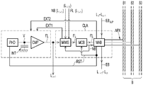
- the pixel comprises a photodetector PHD (typically a photodiode, for example of the "pinned" type), a load integration capacitor INT, a comparator CMP and a logic circuit for access to the bus CLA, connected to a bus B.
- the bus B consists of a plurality (for example, three) elementary buses B1, B2, B3, each comprising a plurality of conductive lines.
- the photodetector assembly - integration capacity - comparator is quite conventional.
- the photodetector PHD when illuminated, generates charges that are integrated by the capacitance INT, varying the voltage V at its terminals.
- the photodetector PHD generates a current I which discharges the capacitor INT, whose initialization voltage is V RST .
- C is the value of INT.
- logic circuit access to the bus CLA can also cause the extinction of the photodetector and the comparator of the pixel in order to mutualize the spatial information of the image; for this purpose, it exchanges signals with its nearest neighbors: it receives a signal from the pixel of the column belonging to line L i-1 of rank immediately below and transmits a signal to the pixel of the column belonging to the line L i + 1 of rank immediately higher. This mechanism will be described later.
- the bus access logic circuit CLA When it receives a trigger signal, after a time T from the reset, the bus access logic circuit CLA seeks to transmit on the first elementary bus, B1, the APX signal. If the elementary bus B1, or any other elementary bus of the bus B, is already occupied by a pixel of lower rank, the circuit CLA gives up the transmission and sends a reset signal RST at the photodetector PHD and at the integrator INT. In other words, the pixels have a higher priority level as their rank is low (the opposite is also possible). After a time T, the comparator generates the trigger signal again, and the circuit CLA makes a new access to the bus. This time, however, access is on the B2 elementary bus.
- the pixel of rank 1 differs from that of the figure 2a only in that it does not receive signals from lower-order pixels because these pixels do not exist. Similarly, the pixel of rank m does not transmit signals to pixels of higher rank.
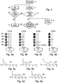
- the logigram of the figure 3 illustrates the operating principle of a pixel PX.
- Step E0 corresponds to the global reset of the matrix.
- the pixel PX (like all the other pixels of the matrix) begins to integrate the photogenerated charges by its photodetector.
- the voltage V across its integration capacitance varies (decreases, in general) linearly, until it reaches the threshold value V TH at a time T.
- the comparator CMP generates the trigger signal FL (step E1).
- the logic circuit CLA checks whether the maximum reset number (2 in the example of the figure 2a ) has been reached (E2). If so, it checks whether the elementary bus of maximum rank, B3, is free (E5), that is to say if it is not occupied by a pixel of higher priority level.
- the logic circuit checks whether the elementary bus corresponds to the number of resets already made (B1 if no reinitialization has taken place, B2 if there are any had a) is free (E3). If the chosen elementary bus is free, it is used to transmit the APX signal to the read circuit (E7), and the pixel turns off. Otherwise, the pixel is reset and a new charge integration step begins.
- FIGS. 5a, 5b, 5c, 5d and 5e are graphs of the voltage V across the the pixel integrator PX1, PX2, PX3, PX4 and PX5, respectively, as a function of time.
- the pixels PX1, PX2, PX4 and PX5 seek to simultaneously access the bus, and more specifically to the elementary bus B1.
- the highest priority level pixel, PX1 manages to transmit its address on the bus, then turns off.
- the pixels PX2, PX4 and PX5 must give up the transmission and reset themselves. Meanwhile, the integration capability of the PX3 pixel is discharged more slowly since the photodetector associated with it receives a lower light intensity.
- the pixels PX2, PX4 and PX5 again seek access to the bus, but this time the access attempt concerns the elementary bus B2, because these pixels have already been reset once during the current frame period .
- the pixel PX3 seeks to access the elementary bus B1.
- the pixel PX1 is off, and no longer intervenes.
- only the highest priority pixel among those attempting to access manages to transmit its address to the reading circuit: it is the pixel PX2 which, after having made the transmission, goes out.
- the pixels PX3, PX4 and PX5 are reset and begin to integrate the photogenerated charges.
- the pixels PX4 and PX5 trigger for the third time, and simultaneously try to access the third elementary bus B3.
- the highest priority pixel - PX4 - transmits its address first, while PX5 does it just after, at a time 3T + T err . After transmitting their address, these pixels go out. It is understood that the estimate of the luminous intensity of the pixel PX5 is slightly distorted by the additional delay T err .
- FIGS. 7a, 7b, 7c, 7d and 7e are graphs of the voltage V across the pixel integrator PX1, PX2, PX3, PX4 and PX5, respectively, as a function of time.
- the pixels PX1, PX2, PX4 and PX5 seek to simultaneously access the bus, and more specifically to the elementary bus B1.
- the highest priority pixel, PX1 manages to transmit its address on the bus and goes off.
- the mechanism for sharing spatial information also causes the extinction of PX2 and PX5, because of collisions with PX1 and PX4, respectively.
- the PX4 pixel is reset.
- the pixel PX3 accesses the elementary bus B1 and PX4 seeks to access the elementary bus B2.
- the conflict is resolved in favor of PX3, whose priority level is higher, while PX4 is reset.
- the mechanism for sharing spatial information does not intervene (and therefore PX4 is not extinguished) because the elementary buses involved are different.
- the transmitted pixel PX4 is APX address on the elementary bus B3.
- FIGS. 7a, 7b, 7c, 7d and 7e are graphs of the voltage V across the pixel integrator PX1, PX2, PX3, PX4 and PX5, respectively, as a function of time.
- the logic circuit for access to the bus CLA comprises three functional blocks: a module for sharing the spatial information MMIS, a choice module for the elementary bus MCB and a bus access module, MAB.
- the MMIS spatial information sharing module comprises an input for the lower-order nearest-neighbor trigger signal, L i-1 , and an input for the pixel-trigger signal FL.
- the module In the event of simultaneous reception of the two signals, the module generates the signal EXT1 which triggers the extinction of the photodetector PHD and the comparator CMP.
- the FL signal is transmitted to the equivalent module of the higher rank pixel, L i + 1 , and the module of choice of the bus, MCB.
- this module can be based on a logic gate "AND" with three inputs, PLE.
- the signals on the three inputs of the PLE gate are the FL trigger signal of the pixel, the trigger signal of the higher order pixel FL (L i + 1 ) and an ERB signal representative of a bitwise equality between the signal NB generated by the MCB module, representative of the selected bus number (see below), and the NB signal of the lower rank pixel, L i-1 .
- the bits NB i (bit1), NB i-1 (bit1), NB i (bit2), NB i-1 (bit2) of the bus numbers are compared two by two with the aid of gates NO -OR EXCLUSIVE NXOR1, NXOR2 whose outputs are provided to an "AND" PLEE.
- the figure 2b refers to the case where the bus numbers are represented by two bits (which allows to use at most four buses), but a generalization does not pose any difficulty.
- the choice module of the MCB bus ( Figure 2c ) is simply constituted by a CMPT counter which is incremented each time it receives the FL trigger signal from the comparator CMP via the MMIS module. Its NB output signal, transmitted to the access module MAB, corresponds to the value of the count and designates the elementary bus chosen. This is a multi-bit signal - 2 in the embodiment considered here, where the three elementary buses B1, B2 and B3 can be designated 00, 01 and 10.
- the trigger signal FL is also transmitted to the MAB access module.
- the CMPT counter is incremented by the pixel reset signal, RST, generated by the MAB module.
- the MAB bus access module ( figure 2d ) is slightly more complex. It has three inputs for: the trigger signal FL from the comparator CMP via the modules MMIS and MCB; a binary signal EB SUP from the block of pixels of the column belonging to lines of lower rank L 1 -L i-1 ; and the NB signal generated by the choice module of the MCB bus; and four outputs for: an extinction signal EXT2 of the photodetector PHD and the comparator CMP; a reset signal RST of the photodetector PHD and the integration capacitor INT, an EB signal representative of the state of the bus, which is transmitted to the block of pixels of the column belonging to lines of higher rank L i + 1 -L m (and constitutes, for the latter, the signal EB SUP ); and the APX signal indicative of the pixel address.
- the complement of the signal EB SUP and the trigger signal FL are applied to the inputs of an "AND" logic gate PLE1.
- the signal SAB is supplied to an input, called activation, of the address multiplexer MXA, which also receives, on another so-called selection input, the signal NB.
- the address multiplexer NB has a plurality of M-bit outputs, connected to respective elementary buses (B1, B2, B3).
- the access multiplexer supplies, on the output determined by the signal NB present on its selection input, the M-bit signal APX, which uniquely identifies the pixel at inside the column.
- An element introducing a delay can be added to the input of the FL signal in the MAB module in order to ensure a good delay of the circuit.
- the signal SAB is taken from an output of the MAB module to constitute the signal EXT2 which, just like EXT1, controls the extinction of the photodetector PHD and the comparator CMP.
- the read circuit receives the APX address signals, applies a time stamp to them and transmits the set (address, bus on which the address was received, time stamp) to a processor that reconstructs the image.
- the reading circuit can directly calculate the luminous intensity associated with each pixel (equation 2) and transmit the calculated value to the processor.
- equation 2 the luminous intensity associated with each pixel
- the number of elementary buses is one of the most important design parameters of an image sensor according to the invention. The higher this number, the lower the probability that the acquisition time of an address signal will be falsified by repeated collisions (the case of the PX5 pixel in Figures 4a - 5e ). However, the number of possible resets is constrained by the frame acquisition rate; in addition, the multiplication of the elementary buses increases the complexity of the circuit. However, it is found that in practice the number of elementary buses can be limited to a few units while ensuring a satisfactory image quality. This is illustrated using Figures 9a - 9d .
- the figure 9a is a reference image, acquired by means of an active pixel CMOS sensor.
- the priority level of a pixel is entirely predetermined and more precisely depends solely on its rank within the column; we can speak of an "intrinsic" priority.
- the priority depends mainly on the elementary bus on which the pixel intends to transmit its address (and therefore the number of transmission attempts already made). We can talk about an "extrinsic" priority.
- the pixels which intend to transmit on the elementary bus B3 have priority over those which intend to transmit on the elementary buses B2 and B1, and those which intend to transmit on B2 take precedence over those which intend to transmit on B1.
- the invention has been described with reference to the case of an image sensor comprising a matrix of pixels each comprising a photodetector. It applies more generally to any kind of matrix sensor comprising an arrangement of detecting elements each comprising an elementary sensor configured to generate an electric current whose intensity is representative of (for example, proportional to) a physical quantity to be detected. It may be, for example, thermal, chemical, pressure sensors, etc.
Landscapes
- Engineering & Computer Science (AREA)
- Signal Processing (AREA)
- Multimedia (AREA)
- Computer Networks & Wireless Communication (AREA)
- Transforming Light Signals Into Electric Signals (AREA)
- Solid State Image Pick-Up Elements (AREA)
Applications Claiming Priority (1)
| Application Number | Priority Date | Filing Date | Title |
|---|---|---|---|
| FR1753032A FR3065133B1 (fr) | 2017-04-07 | 2017-04-07 | Capteur matriciel a codage temporel sans arbitrage |
Publications (2)
| Publication Number | Publication Date |
|---|---|
| EP3386191A1 true EP3386191A1 (de) | 2018-10-10 |
| EP3386191B1 EP3386191B1 (de) | 2019-07-31 |
Family
ID=59974497
Family Applications (1)
| Application Number | Title | Priority Date | Filing Date |
|---|---|---|---|
| EP18164285.1A Active EP3386191B1 (de) | 2017-04-07 | 2018-03-27 | Array-sensor mit zeitkodierung ohne arbitrierung |
Country Status (3)
| Country | Link |
|---|---|
| US (1) | US10341587B2 (de) |
| EP (1) | EP3386191B1 (de) |
| FR (1) | FR3065133B1 (de) |
Cited By (1)
| Publication number | Priority date | Publication date | Assignee | Title |
|---|---|---|---|---|
| US10721007B2 (en) * | 2015-12-04 | 2020-07-21 | Infineon Technologies Ag | Robust high speed sensor interface for remote sensors |
Families Citing this family (2)
| Publication number | Priority date | Publication date | Assignee | Title |
|---|---|---|---|---|
| FR3116640B1 (fr) | 2020-11-20 | 2023-11-17 | Commissariat Energie Atomique | Procédé itératif d’estimation du mouvement d’un corps matériel par génération d’une grille de mouvement filtrée |
| CN115687911B (zh) * | 2022-06-13 | 2023-06-02 | 北京融合未来技术有限公司 | 基于脉冲信号的信号灯检测方法、装置和系统 |
Citations (5)
| Publication number | Priority date | Publication date | Assignee | Title |
|---|---|---|---|---|
| US6253161B1 (en) * | 1997-07-10 | 2001-06-26 | Universite Laval | Integrated motion vision sensor |
| US20050273661A1 (en) * | 2004-05-20 | 2005-12-08 | Vladimir Brajovic | Method for determining identity of simultaneous events and applications to image sensing and A/D conversion |
| US20100182468A1 (en) * | 2006-11-23 | 2010-07-22 | Austrian Research Centers Gmbh-Arc | Method for the generation of an image in electronic form, picture element (pixel) for an image sensor for the generation of an image as well as image sensor |
| WO2014174498A1 (en) * | 2013-04-26 | 2014-10-30 | Ecole Polytechnique Federale De Lausanne (Epfl) | A novel cmos image sensor with event/change detection and reduced data redundancy |
| FR3035759A1 (fr) * | 2015-04-28 | 2016-11-04 | Commissariat Energie Atomique | Capteur d'images a codage temporel |
Family Cites Families (2)
| Publication number | Priority date | Publication date | Assignee | Title |
|---|---|---|---|---|
| WO2013070942A1 (en) * | 2011-11-08 | 2013-05-16 | Rambus Inc. | Image sensor sampled at non-uniform intervals |
| US9743024B2 (en) * | 2015-07-01 | 2017-08-22 | Massachusetts Institute Of Technology | Method and apparatus for on-chip per-pixel pseudo-random time coded exposure |
-
2017
- 2017-04-07 FR FR1753032A patent/FR3065133B1/fr not_active Expired - Fee Related
-
2018
- 2018-03-27 EP EP18164285.1A patent/EP3386191B1/de active Active
- 2018-04-05 US US15/946,653 patent/US10341587B2/en active Active
Patent Citations (5)
| Publication number | Priority date | Publication date | Assignee | Title |
|---|---|---|---|---|
| US6253161B1 (en) * | 1997-07-10 | 2001-06-26 | Universite Laval | Integrated motion vision sensor |
| US20050273661A1 (en) * | 2004-05-20 | 2005-12-08 | Vladimir Brajovic | Method for determining identity of simultaneous events and applications to image sensing and A/D conversion |
| US20100182468A1 (en) * | 2006-11-23 | 2010-07-22 | Austrian Research Centers Gmbh-Arc | Method for the generation of an image in electronic form, picture element (pixel) for an image sensor for the generation of an image as well as image sensor |
| WO2014174498A1 (en) * | 2013-04-26 | 2014-10-30 | Ecole Polytechnique Federale De Lausanne (Epfl) | A novel cmos image sensor with event/change detection and reduced data redundancy |
| FR3035759A1 (fr) * | 2015-04-28 | 2016-11-04 | Commissariat Energie Atomique | Capteur d'images a codage temporel |
Non-Patent Citations (1)
| Title |
|---|
| NICOLA MASSARI ET AL: "A collision-free time-to-first spike camera architecture based on a winner-take-all network", CIRCUIT THEORY AND DESIGN, 2007. ECCTD 2007. 18TH EUROPEAN CONFERENCE ON, IEEE, PISCATAWAY, NJ, USA, 27 August 2007 (2007-08-27), pages 950 - 953, XP031257906, ISBN: 978-1-4244-1341-6 * |
Cited By (3)
| Publication number | Priority date | Publication date | Assignee | Title |
|---|---|---|---|---|
| US10721007B2 (en) * | 2015-12-04 | 2020-07-21 | Infineon Technologies Ag | Robust high speed sensor interface for remote sensors |
| US11018788B2 (en) | 2015-12-04 | 2021-05-25 | Infineon Technologies Ag | Robust high speed sensor interface for remote sensors |
| US11728916B2 (en) | 2015-12-04 | 2023-08-15 | Infineon Technologies Ag | Robust high speed sensor interface for remote sensors |
Also Published As
| Publication number | Publication date |
|---|---|
| US20180295308A1 (en) | 2018-10-11 |
| EP3386191B1 (de) | 2019-07-31 |
| FR3065133A1 (fr) | 2018-10-12 |
| US10341587B2 (en) | 2019-07-02 |
| FR3065133B1 (fr) | 2019-06-21 |
Similar Documents
| Publication | Publication Date | Title |
|---|---|---|
| EP2477393B1 (de) | Bildanzeigevorrichtung mit großem dynamischem Bereich | |
| EP3721616B1 (de) | Bildsensor mit hohem dynamikbereich | |
| FR3039928B1 (fr) | Procede de commande d'un capteur d'image a pixels actifs | |
| EP2567540B1 (de) | Linearer streifenbildsensor mit analoger und digitaler summierung und entsprechendes verfahren | |
| EP2846533B1 (de) | Vorrichtung zur komprimierten Bilderfassung | |
| EP2064867B1 (de) | Bewegung eines bildsensors mittels sukzessiver integration und summierung mit aktiven cmos-pixeln | |
| EP3386191B1 (de) | Array-sensor mit zeitkodierung ohne arbitrierung | |
| FR2961021A1 (fr) | Capteur d'image linéaire en technologie cmos a compensation d'effet de file | |
| EP2926162A1 (de) | Verfahren zur herstellung von bildern mit tiefeninformationen und bildsensor | |
| FR3002824A1 (fr) | Procede et dispositif de generation d'images a grande gamme dynamique | |
| FR3042912A1 (fr) | Capteur d'images a grande gamme dynamique | |
| FR2973162A1 (fr) | Capteur d'image a tres haute dynamique | |
| JP2024513276A (ja) | 画像センサ、その画像出力方法及び使用 | |
| EP2243287A1 (de) | Sichtsensor zur messung von kontrasten und verfahren zur durchführung einer solchen messung | |
| WO2008034677A1 (fr) | Capteur d'image lineaire cmos a fonctionnement de type transfert de charges | |
| EP2408194B1 (de) | Bilderfassungsgerät mit CMOS-Technologie mit einer starken Videofrequenz | |
| WO2017125316A1 (fr) | Procede de commande d'un capteur d'image a pixels actifs | |
| FR2589302A1 (fr) | Systeme de thermographie infrarouge a sensibilite amelioree par accumulation progressive des lignes de l'image | |
| JP2002165137A (ja) | ディジタル画素センサ読出し情報内の画素の再配置のための回路及び方法 | |
| FR3006500A1 (fr) | Capteur cmos a photosites standard | |
| EP3310039B1 (de) | Elektronische vorrichtung zur analyse einer szene | |
| EP4186227B1 (de) | Flugzeitsensor für abstandsmessung mit pixel mit mehreren speicherknoten | |
| US12369414B2 (en) | Photoelectric conversion device | |
| EP4729981A1 (de) | Pixel und abstandssensor | |
| FR2913784A1 (fr) | Gestion de donnees pour un traitement d'images |
Legal Events
| Date | Code | Title | Description |
|---|---|---|---|
| PUAI | Public reference made under article 153(3) epc to a published international application that has entered the european phase |
Free format text: ORIGINAL CODE: 0009012 |
|
| STAA | Information on the status of an ep patent application or granted ep patent |
Free format text: STATUS: REQUEST FOR EXAMINATION WAS MADE |
|
| 17P | Request for examination filed |
Effective date: 20180327 |
|
| AK | Designated contracting states |
Kind code of ref document: A1 Designated state(s): AL AT BE BG CH CY CZ DE DK EE ES FI FR GB GR HR HU IE IS IT LI LT LU LV MC MK MT NL NO PL PT RO RS SE SI SK SM TR |
|
| AX | Request for extension of the european patent |
Extension state: BA ME |
|
| GRAP | Despatch of communication of intention to grant a patent |
Free format text: ORIGINAL CODE: EPIDOSNIGR1 |
|
| STAA | Information on the status of an ep patent application or granted ep patent |
Free format text: STATUS: GRANT OF PATENT IS INTENDED |
|
| RIC1 | Information provided on ipc code assigned before grant |
Ipc: H04L 1/12 20060101ALI20190307BHEP Ipc: H04N 5/374 20110101ALI20190307BHEP Ipc: H04N 5/378 20110101AFI20190307BHEP Ipc: H04N 5/3745 20110101ALI20190307BHEP |
|
| INTG | Intention to grant announced |
Effective date: 20190326 |
|
| GRAS | Grant fee paid |
Free format text: ORIGINAL CODE: EPIDOSNIGR3 |
|
| GRAA | (expected) grant |
Free format text: ORIGINAL CODE: 0009210 |
|
| STAA | Information on the status of an ep patent application or granted ep patent |
Free format text: STATUS: THE PATENT HAS BEEN GRANTED |
|
| AK | Designated contracting states |
Kind code of ref document: B1 Designated state(s): AL AT BE BG CH CY CZ DE DK EE ES FI FR GB GR HR HU IE IS IT LI LT LU LV MC MK MT NL NO PL PT RO RS SE SI SK SM TR |
|
| REG | Reference to a national code |
Ref country code: CH Ref legal event code: EP Ref country code: GB Ref legal event code: FG4D Free format text: NOT ENGLISH |
|
| REG | Reference to a national code |
Ref country code: AT Ref legal event code: REF Ref document number: 1162255 Country of ref document: AT Kind code of ref document: T Effective date: 20190815 |
|
| REG | Reference to a national code |
Ref country code: IE Ref legal event code: FG4D Free format text: LANGUAGE OF EP DOCUMENT: FRENCH |
|
| REG | Reference to a national code |
Ref country code: DE Ref legal event code: R096 Ref document number: 602018000331 Country of ref document: DE |
|
| REG | Reference to a national code |
Ref country code: NL Ref legal event code: MP Effective date: 20190731 |
|
| REG | Reference to a national code |
Ref country code: LT Ref legal event code: MG4D |
|
| REG | Reference to a national code |
Ref country code: AT Ref legal event code: MK05 Ref document number: 1162255 Country of ref document: AT Kind code of ref document: T Effective date: 20190731 |
|
| PG25 | Lapsed in a contracting state [announced via postgrant information from national office to epo] |
Ref country code: FI Free format text: LAPSE BECAUSE OF FAILURE TO SUBMIT A TRANSLATION OF THE DESCRIPTION OR TO PAY THE FEE WITHIN THE PRESCRIBED TIME-LIMIT Effective date: 20190731 Ref country code: HR Free format text: LAPSE BECAUSE OF FAILURE TO SUBMIT A TRANSLATION OF THE DESCRIPTION OR TO PAY THE FEE WITHIN THE PRESCRIBED TIME-LIMIT Effective date: 20190731 Ref country code: BG Free format text: LAPSE BECAUSE OF FAILURE TO SUBMIT A TRANSLATION OF THE DESCRIPTION OR TO PAY THE FEE WITHIN THE PRESCRIBED TIME-LIMIT Effective date: 20191031 Ref country code: NL Free format text: LAPSE BECAUSE OF FAILURE TO SUBMIT A TRANSLATION OF THE DESCRIPTION OR TO PAY THE FEE WITHIN THE PRESCRIBED TIME-LIMIT Effective date: 20190731 Ref country code: LT Free format text: LAPSE BECAUSE OF FAILURE TO SUBMIT A TRANSLATION OF THE DESCRIPTION OR TO PAY THE FEE WITHIN THE PRESCRIBED TIME-LIMIT Effective date: 20190731 Ref country code: SE Free format text: LAPSE BECAUSE OF FAILURE TO SUBMIT A TRANSLATION OF THE DESCRIPTION OR TO PAY THE FEE WITHIN THE PRESCRIBED TIME-LIMIT Effective date: 20190731 Ref country code: PT Free format text: LAPSE BECAUSE OF FAILURE TO SUBMIT A TRANSLATION OF THE DESCRIPTION OR TO PAY THE FEE WITHIN THE PRESCRIBED TIME-LIMIT Effective date: 20191202 Ref country code: AT Free format text: LAPSE BECAUSE OF FAILURE TO SUBMIT A TRANSLATION OF THE DESCRIPTION OR TO PAY THE FEE WITHIN THE PRESCRIBED TIME-LIMIT Effective date: 20190731 Ref country code: NO Free format text: LAPSE BECAUSE OF FAILURE TO SUBMIT A TRANSLATION OF THE DESCRIPTION OR TO PAY THE FEE WITHIN THE PRESCRIBED TIME-LIMIT Effective date: 20191031 |
|
| PG25 | Lapsed in a contracting state [announced via postgrant information from national office to epo] |
Ref country code: GR Free format text: LAPSE BECAUSE OF FAILURE TO SUBMIT A TRANSLATION OF THE DESCRIPTION OR TO PAY THE FEE WITHIN THE PRESCRIBED TIME-LIMIT Effective date: 20191101 Ref country code: AL Free format text: LAPSE BECAUSE OF FAILURE TO SUBMIT A TRANSLATION OF THE DESCRIPTION OR TO PAY THE FEE WITHIN THE PRESCRIBED TIME-LIMIT Effective date: 20190731 Ref country code: ES Free format text: LAPSE BECAUSE OF FAILURE TO SUBMIT A TRANSLATION OF THE DESCRIPTION OR TO PAY THE FEE WITHIN THE PRESCRIBED TIME-LIMIT Effective date: 20190731 Ref country code: RS Free format text: LAPSE BECAUSE OF FAILURE TO SUBMIT A TRANSLATION OF THE DESCRIPTION OR TO PAY THE FEE WITHIN THE PRESCRIBED TIME-LIMIT Effective date: 20190731 Ref country code: IS Free format text: LAPSE BECAUSE OF FAILURE TO SUBMIT A TRANSLATION OF THE DESCRIPTION OR TO PAY THE FEE WITHIN THE PRESCRIBED TIME-LIMIT Effective date: 20191130 Ref country code: LV Free format text: LAPSE BECAUSE OF FAILURE TO SUBMIT A TRANSLATION OF THE DESCRIPTION OR TO PAY THE FEE WITHIN THE PRESCRIBED TIME-LIMIT Effective date: 20190731 |
|
| PG25 | Lapsed in a contracting state [announced via postgrant information from national office to epo] |
Ref country code: TR Free format text: LAPSE BECAUSE OF FAILURE TO SUBMIT A TRANSLATION OF THE DESCRIPTION OR TO PAY THE FEE WITHIN THE PRESCRIBED TIME-LIMIT Effective date: 20190731 |
|
| PG25 | Lapsed in a contracting state [announced via postgrant information from national office to epo] |
Ref country code: PL Free format text: LAPSE BECAUSE OF FAILURE TO SUBMIT A TRANSLATION OF THE DESCRIPTION OR TO PAY THE FEE WITHIN THE PRESCRIBED TIME-LIMIT Effective date: 20190731 Ref country code: EE Free format text: LAPSE BECAUSE OF FAILURE TO SUBMIT A TRANSLATION OF THE DESCRIPTION OR TO PAY THE FEE WITHIN THE PRESCRIBED TIME-LIMIT Effective date: 20190731 Ref country code: DK Free format text: LAPSE BECAUSE OF FAILURE TO SUBMIT A TRANSLATION OF THE DESCRIPTION OR TO PAY THE FEE WITHIN THE PRESCRIBED TIME-LIMIT Effective date: 20190731 Ref country code: IT Free format text: LAPSE BECAUSE OF FAILURE TO SUBMIT A TRANSLATION OF THE DESCRIPTION OR TO PAY THE FEE WITHIN THE PRESCRIBED TIME-LIMIT Effective date: 20190731 Ref country code: RO Free format text: LAPSE BECAUSE OF FAILURE TO SUBMIT A TRANSLATION OF THE DESCRIPTION OR TO PAY THE FEE WITHIN THE PRESCRIBED TIME-LIMIT Effective date: 20190731 |
|
| PG25 | Lapsed in a contracting state [announced via postgrant information from national office to epo] |
Ref country code: IS Free format text: LAPSE BECAUSE OF FAILURE TO SUBMIT A TRANSLATION OF THE DESCRIPTION OR TO PAY THE FEE WITHIN THE PRESCRIBED TIME-LIMIT Effective date: 20200224 Ref country code: SM Free format text: LAPSE BECAUSE OF FAILURE TO SUBMIT A TRANSLATION OF THE DESCRIPTION OR TO PAY THE FEE WITHIN THE PRESCRIBED TIME-LIMIT Effective date: 20190731 Ref country code: CZ Free format text: LAPSE BECAUSE OF FAILURE TO SUBMIT A TRANSLATION OF THE DESCRIPTION OR TO PAY THE FEE WITHIN THE PRESCRIBED TIME-LIMIT Effective date: 20190731 Ref country code: SK Free format text: LAPSE BECAUSE OF FAILURE TO SUBMIT A TRANSLATION OF THE DESCRIPTION OR TO PAY THE FEE WITHIN THE PRESCRIBED TIME-LIMIT Effective date: 20190731 |
|
| REG | Reference to a national code |
Ref country code: DE Ref legal event code: R097 Ref document number: 602018000331 Country of ref document: DE |
|
| PLBE | No opposition filed within time limit |
Free format text: ORIGINAL CODE: 0009261 |
|
| STAA | Information on the status of an ep patent application or granted ep patent |
Free format text: STATUS: NO OPPOSITION FILED WITHIN TIME LIMIT |
|
| PG2D | Information on lapse in contracting state deleted |
Ref country code: IS |
|
| PG25 | Lapsed in a contracting state [announced via postgrant information from national office to epo] |
Ref country code: IS Free format text: LAPSE BECAUSE OF FAILURE TO SUBMIT A TRANSLATION OF THE DESCRIPTION OR TO PAY THE FEE WITHIN THE PRESCRIBED TIME-LIMIT Effective date: 20191030 |
|
| 26N | No opposition filed |
Effective date: 20200603 |
|
| PG25 | Lapsed in a contracting state [announced via postgrant information from national office to epo] |
Ref country code: SI Free format text: LAPSE BECAUSE OF FAILURE TO SUBMIT A TRANSLATION OF THE DESCRIPTION OR TO PAY THE FEE WITHIN THE PRESCRIBED TIME-LIMIT Effective date: 20190731 |
|
| PG25 | Lapsed in a contracting state [announced via postgrant information from national office to epo] |
Ref country code: MC Free format text: LAPSE BECAUSE OF FAILURE TO SUBMIT A TRANSLATION OF THE DESCRIPTION OR TO PAY THE FEE WITHIN THE PRESCRIBED TIME-LIMIT Effective date: 20190731 |
|
| REG | Reference to a national code |
Ref country code: BE Ref legal event code: MM Effective date: 20200331 |
|
| PG25 | Lapsed in a contracting state [announced via postgrant information from national office to epo] |
Ref country code: LU Free format text: LAPSE BECAUSE OF NON-PAYMENT OF DUE FEES Effective date: 20200327 |
|
| PG25 | Lapsed in a contracting state [announced via postgrant information from national office to epo] |
Ref country code: IE Free format text: LAPSE BECAUSE OF NON-PAYMENT OF DUE FEES Effective date: 20200327 |
|
| PG25 | Lapsed in a contracting state [announced via postgrant information from national office to epo] |
Ref country code: BE Free format text: LAPSE BECAUSE OF NON-PAYMENT OF DUE FEES Effective date: 20200331 |
|
| REG | Reference to a national code |
Ref country code: CH Ref legal event code: PL |
|
| PG25 | Lapsed in a contracting state [announced via postgrant information from national office to epo] |
Ref country code: CH Free format text: LAPSE BECAUSE OF NON-PAYMENT OF DUE FEES Effective date: 20210331 Ref country code: LI Free format text: LAPSE BECAUSE OF NON-PAYMENT OF DUE FEES Effective date: 20210331 |
|
| PG25 | Lapsed in a contracting state [announced via postgrant information from national office to epo] |
Ref country code: MT Free format text: LAPSE BECAUSE OF FAILURE TO SUBMIT A TRANSLATION OF THE DESCRIPTION OR TO PAY THE FEE WITHIN THE PRESCRIBED TIME-LIMIT Effective date: 20190731 Ref country code: CY Free format text: LAPSE BECAUSE OF FAILURE TO SUBMIT A TRANSLATION OF THE DESCRIPTION OR TO PAY THE FEE WITHIN THE PRESCRIBED TIME-LIMIT Effective date: 20190731 |
|
| PG25 | Lapsed in a contracting state [announced via postgrant information from national office to epo] |
Ref country code: MK Free format text: LAPSE BECAUSE OF FAILURE TO SUBMIT A TRANSLATION OF THE DESCRIPTION OR TO PAY THE FEE WITHIN THE PRESCRIBED TIME-LIMIT Effective date: 20190731 |
|
| GBPC | Gb: european patent ceased through non-payment of renewal fee |
Effective date: 20220327 |
|
| REG | Reference to a national code |
Ref country code: DE Ref legal event code: R079 Ref document number: 602018000331 Country of ref document: DE Free format text: PREVIOUS MAIN CLASS: H04N0005378000 Ipc: H04N0025780000 |
|
| PG25 | Lapsed in a contracting state [announced via postgrant information from national office to epo] |
Ref country code: GB Free format text: LAPSE BECAUSE OF NON-PAYMENT OF DUE FEES Effective date: 20220327 |
|
| PGFP | Annual fee paid to national office [announced via postgrant information from national office to epo] |
Ref country code: DE Payment date: 20260320 Year of fee payment: 9 |
|
| PGFP | Annual fee paid to national office [announced via postgrant information from national office to epo] |
Ref country code: FR Payment date: 20260318 Year of fee payment: 9 |