EP3389082A1 - Verfahren zur herstellung eines siliciumcarbidhalbleiterbauelements, verfahren zur herstellung eines siliciumcarbidhalbleiterbasiskörpers, siliciumcarbidhalbleiterbauelement und vorrichtung zur herstellung eines siliciumcarbidhalbleiterbauelements - Google Patents
Verfahren zur herstellung eines siliciumcarbidhalbleiterbauelements, verfahren zur herstellung eines siliciumcarbidhalbleiterbasiskörpers, siliciumcarbidhalbleiterbauelement und vorrichtung zur herstellung eines siliciumcarbidhalbleiterbauelements Download PDFInfo
- Publication number
- EP3389082A1 EP3389082A1 EP15884168.4A EP15884168A EP3389082A1 EP 3389082 A1 EP3389082 A1 EP 3389082A1 EP 15884168 A EP15884168 A EP 15884168A EP 3389082 A1 EP3389082 A1 EP 3389082A1
- Authority
- EP
- European Patent Office
- Prior art keywords
- silicon carbide
- laser light
- metal layer
- wafer
- semiconductor device
- Prior art date
- Legal status (The legal status is an assumption and is not a legal conclusion. Google has not performed a legal analysis and makes no representation as to the accuracy of the status listed.)
- Granted
Links
Images




Classifications
-
- H—ELECTRICITY
- H10—SEMICONDUCTOR DEVICES; ELECTRIC SOLID-STATE DEVICES NOT OTHERWISE PROVIDED FOR
- H10D—INORGANIC ELECTRIC SEMICONDUCTOR DEVICES
- H10D62/00—Semiconductor bodies, or regions thereof, of devices having potential barriers
- H10D62/80—Semiconductor bodies, or regions thereof, of devices having potential barriers characterised by the materials
- H10D62/83—Semiconductor bodies, or regions thereof, of devices having potential barriers characterised by the materials being Group IV materials, e.g. B-doped Si or undoped Ge
- H10D62/832—Semiconductor bodies, or regions thereof, of devices having potential barriers characterised by the materials being Group IV materials, e.g. B-doped Si or undoped Ge being Group IV materials comprising two or more elements, e.g. SiGe
- H10D62/8325—Silicon carbide
-
- H—ELECTRICITY
- H10—SEMICONDUCTOR DEVICES; ELECTRIC SOLID-STATE DEVICES NOT OTHERWISE PROVIDED FOR
- H10D—INORGANIC ELECTRIC SEMICONDUCTOR DEVICES
- H10D62/00—Semiconductor bodies, or regions thereof, of devices having potential barriers
- H10D62/10—Shapes, relative sizes or dispositions of the regions of the semiconductor bodies; Shapes of the semiconductor bodies
- H10D62/102—Constructional design considerations for preventing surface leakage or controlling electric field concentration
- H10D62/103—Constructional design considerations for preventing surface leakage or controlling electric field concentration for increasing or controlling the breakdown voltage of reverse-biased devices
- H10D62/105—Constructional design considerations for preventing surface leakage or controlling electric field concentration for increasing or controlling the breakdown voltage of reverse-biased devices by having particular doping profiles, shapes or arrangements of PN junctions; by having supplementary regions, e.g. junction termination extension [JTE]
- H10D62/106—Constructional design considerations for preventing surface leakage or controlling electric field concentration for increasing or controlling the breakdown voltage of reverse-biased devices by having particular doping profiles, shapes or arrangements of PN junctions; by having supplementary regions, e.g. junction termination extension [JTE] having supplementary regions doped oppositely to or in rectifying contact with regions of the semiconductor bodies, e.g. guard rings with PN or Schottky junctions
-
- H—ELECTRICITY
- H10—SEMICONDUCTOR DEVICES; ELECTRIC SOLID-STATE DEVICES NOT OTHERWISE PROVIDED FOR
- H10D—INORGANIC ELECTRIC SEMICONDUCTOR DEVICES
- H10D64/00—Electrodes of devices having potential barriers
- H10D64/01—Manufacture or treatment
- H10D64/011—Manufacture or treatment of electrodes ohmically coupled to a semiconductor
- H10D64/0111—Manufacture or treatment of electrodes ohmically coupled to a semiconductor to Group IV semiconductors
-
- H—ELECTRICITY
- H10—SEMICONDUCTOR DEVICES; ELECTRIC SOLID-STATE DEVICES NOT OTHERWISE PROVIDED FOR
- H10D—INORGANIC ELECTRIC SEMICONDUCTOR DEVICES
- H10D64/00—Electrodes of devices having potential barriers
- H10D64/01—Manufacture or treatment
- H10D64/011—Manufacture or treatment of electrodes ohmically coupled to a semiconductor
- H10D64/0111—Manufacture or treatment of electrodes ohmically coupled to a semiconductor to Group IV semiconductors
- H10D64/0115—Manufacture or treatment of electrodes ohmically coupled to a semiconductor to Group IV semiconductors to silicon carbide
-
- H—ELECTRICITY
- H10—SEMICONDUCTOR DEVICES; ELECTRIC SOLID-STATE DEVICES NOT OTHERWISE PROVIDED FOR
- H10P—GENERIC PROCESSES OR APPARATUS FOR THE MANUFACTURE OR TREATMENT OF DEVICES COVERED BY CLASS H10
- H10P14/00—Formation of materials, e.g. in the shape of layers or pillars
- H10P14/20—Formation of materials, e.g. in the shape of layers or pillars of semiconductor materials
- H10P14/34—Deposited materials, e.g. layers
- H10P14/3402—Deposited materials, e.g. layers characterised by the chemical composition
- H10P14/3404—Deposited materials, e.g. layers characterised by the chemical composition being Group IVA materials
- H10P14/3408—Silicon carbide
-
- H—ELECTRICITY
- H10—SEMICONDUCTOR DEVICES; ELECTRIC SOLID-STATE DEVICES NOT OTHERWISE PROVIDED FOR
- H10P—GENERIC PROCESSES OR APPARATUS FOR THE MANUFACTURE OR TREATMENT OF DEVICES COVERED BY CLASS H10
- H10P34/00—Irradiation with electromagnetic or particle radiation of wafers, substrates or parts of devices
- H10P34/40—Irradiation with electromagnetic or particle radiation of wafers, substrates or parts of devices with high-energy radiation
- H10P34/42—Irradiation with electromagnetic or particle radiation of wafers, substrates or parts of devices with high-energy radiation with electromagnetic radiation, e.g. laser annealing
-
- H—ELECTRICITY
- H10—SEMICONDUCTOR DEVICES; ELECTRIC SOLID-STATE DEVICES NOT OTHERWISE PROVIDED FOR
- H10P—GENERIC PROCESSES OR APPARATUS FOR THE MANUFACTURE OR TREATMENT OF DEVICES COVERED BY CLASS H10
- H10P54/00—Cutting or separating of wafers, substrates or parts of devices
-
- H—ELECTRICITY
- H10—SEMICONDUCTOR DEVICES; ELECTRIC SOLID-STATE DEVICES NOT OTHERWISE PROVIDED FOR
- H10P—GENERIC PROCESSES OR APPARATUS FOR THE MANUFACTURE OR TREATMENT OF DEVICES COVERED BY CLASS H10
- H10P70/00—Cleaning of wafers, substrates or parts of devices
- H10P70/20—Cleaning during device manufacture
-
- H—ELECTRICITY
- H10—SEMICONDUCTOR DEVICES; ELECTRIC SOLID-STATE DEVICES NOT OTHERWISE PROVIDED FOR
- H10W—GENERIC PACKAGES, INTERCONNECTIONS, CONNECTORS OR OTHER CONSTRUCTIONAL DETAILS OF DEVICES COVERED BY CLASS H10
- H10W46/00—Marks applied to devices, e.g. for alignment or identification
-
- H—ELECTRICITY
- H10—SEMICONDUCTOR DEVICES; ELECTRIC SOLID-STATE DEVICES NOT OTHERWISE PROVIDED FOR
- H10W—GENERIC PACKAGES, INTERCONNECTIONS, CONNECTORS OR OTHER CONSTRUCTIONAL DETAILS OF DEVICES COVERED BY CLASS H10
- H10W46/00—Marks applied to devices, e.g. for alignment or identification
- H10W46/301—Marks applied to devices, e.g. for alignment or identification for alignment
-
- H—ELECTRICITY
- H10—SEMICONDUCTOR DEVICES; ELECTRIC SOLID-STATE DEVICES NOT OTHERWISE PROVIDED FOR
- H10W—GENERIC PACKAGES, INTERCONNECTIONS, CONNECTORS OR OTHER CONSTRUCTIONAL DETAILS OF DEVICES COVERED BY CLASS H10
- H10W74/00—Encapsulations, e.g. protective coatings
- H10W74/01—Manufacture or treatment
- H10W74/014—Manufacture or treatment using batch processing
-
- H—ELECTRICITY
- H10—SEMICONDUCTOR DEVICES; ELECTRIC SOLID-STATE DEVICES NOT OTHERWISE PROVIDED FOR
- H10W—GENERIC PACKAGES, INTERCONNECTIONS, CONNECTORS OR OTHER CONSTRUCTIONAL DETAILS OF DEVICES COVERED BY CLASS H10
- H10W74/00—Encapsulations, e.g. protective coatings
- H10W74/10—Encapsulations, e.g. protective coatings characterised by their shape or disposition
- H10W74/131—Encapsulations, e.g. protective coatings characterised by their shape or disposition the semiconductor body being only partially enclosed
- H10W74/137—Encapsulations, e.g. protective coatings characterised by their shape or disposition the semiconductor body being only partially enclosed the encapsulations being directly on the semiconductor body
Definitions
- the present invention relates to a method for manufacturing a silicon carbide semiconductor device, a method for manufacturing a semiconductor base, a silicon carbide semiconductor device, and a device for manufacturing a silicon carbide semiconductor device.
- the present invention provides a method for manufacturing a silicon carbide semiconductor device, a method for manufacturing a semiconductor base, a silicon carbide semiconductor device, and a device for manufacturing a silicon carbide semiconductor device, with which warpage is eliminated or reduced in a thinned silicon carbide wafer by a simple technique without removing an affected layer, unlike conventional WO2012/049792 .
- a method for manufacturing a silicon carbide semiconductor device comprises:
- the laser light irradiation may be performed such that a portion to be irradiated with laser light partially overlaps with a portion which was irradiated with the laser light, a high-density portion having high carbide density may be formed by overlapping of portions irradiated with the laser light, and wherein a low-density portion having low carbide density may be formed by non-overlapping of portions irradiated with the laser light.
- the laser light irradiation may be performed such that a portion to be irradiated with laser light partially overlaps with a portion which was irradiated with the laser light, a low-density portion having low carbide density may be formed by overlapping of portions irradiated with the laser light, and a high-density portion having high carbide density may be formed by non-overlapping of portions irradiated with the laser light.
- the laser light irradiation is performed along a first direction, wherein when a particular laser light irradiation is finished along the first direction, another laser light irradiation, starting from another position spaced apart at an interval, is performed along the first direction.
- the external force is applied by an adsorption power by a vacuum adsorption unit, or by a pressing force by a pressing unit made of a member which transmits the laser light.
- the metal layer is titanium, molybdenum, or titanium and molybdenum.
- the laser light is green laser.
- a method for manufacturing a semiconductor base comprises:
- a silicon carbide semiconductor device comprises:
- a manufacturing device comprises:
- the present invention it is possible to eliminate or reduce warpage of the thinned silicon carbide wafer by irradiating the metal layer with laser light to form, not a silicide layer but the carbide layer, while applying an external force such that the silicon carbide wafer and the metal layer are planarized. Consequently, unlike the conventional technique provided by WO2012/049792 , it is possible to eliminate or reduce warpage of the thinned silicon carbide wafer by a simple technique without removing an affected layer.
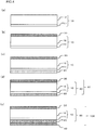
- a method for manufacturing a silicon carbide semiconductor device in the embodiment includes, as illustrated in Fig. 1 , a step for forming a front-surface electrode 30 including metal on a front surface side of a silicon carbide wafer 10 (front-surface electrode formation step S15, see Fig. 4(b) ), and a step for thinning the silicon carbide wafer 10 by reducing the thickness of the silicon carbide wafer 10 from a back surface side thereof (thinning step S16).
- the silicon carbide wafer 10 prepared in Fig. 4(a) includes, for example, a silicon carbide substrate 11 and a silicon carbide layer 12 formed on the silicon carbide substrate 11, for example, by epitaxial growth.
- the method for manufacturing the silicon carbide semiconductor device 100 includes a step for forming a carbide layer 20 (carbide layer formation step S20) .
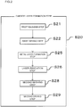
- the carbide layer formation step S20 includes, as illustrated in Fig. 2 , a step for providing a metal layer 21 on the back surface of the thinned silicon carbide wafer 10 (metal layer formation step S25, see Fig.
- the entire metal layer 21 is changed into the carbide layer 20
- there is no limitation thereto only a part of the metal layer 21 on the back surface side thereof (a lower part of the metal layer 21 in Fig. 4(c) ) may be changed into the carbide layer 20, and a part of the metal layer 21 on the front surface side thereof (an upper part of the metal layer 21 in Fig. 4(c) ) may remain unchanged as the metal layer 21.
- by changing the entire metal layer 21 into the carbide layer 20 it is possible to more surely suppress warpage of the thinned silicon carbide wafer 10 (or a front-surface electrode-equipped silicon carbide base 51 described later) .
- the method for manufacturing the silicon carbide semiconductor device 100 includes a step for forming a back-surface electrode 40 including metal on a back surface side of the carbide layer 20 (back-surface electrode formation step S31, see Fig. 4(e) ).
- back-surface electrode formation step S31 see Fig. 4(e)
- a description will be given using, as an example, an aspect in which the front-surface electrode formation step S15, the thinning step S16, the metal layer formation step S25, the laser irradiation step S26, and the back-surface electrode formation step S31 are formed in order.
- the order of these steps can be appropriately changed.
- warpage of the silicon carbide wafer 10 generated in the thinning step S16 can be suppressed by performing the front-surface electrode formation step S15 prior to the thinning step S16, it is preferable to perform the front-surface electrode formation step S15 prior to the thinning step S16 from this viewpoint.
- the carbide layer formation step S20 includes a step for washing at least a back surface of the silicon carbide wafer 10 subjected to the thinning step S16 (first washing step S21), and a step for drying the silicon carbide wafer 10 subjected to the first washing step S21 (first drying step S22) .
- the carbide layer formation step S20 includes a step for washing a silicon carbide base 50 subjected to the laser irradiation step S26 and including the carbide layer 20 formed therein (second washing step S28), and a step for drying the silicon carbide wafer 10 subjected to the second washing step S28 (second drying step S29).
- the silicon carbide wafer 10 or the silicon carbide base 50 is rotated and dried (spin dry).
- the "silicon carbide base 50" means the silicon carbide wafer 10 including the carbide layer 20 formed on the back surface side thereof (see Fig. 3 ).
- the carbide layer 20, and the front-surface electrode 30 is indicated as the front-surface electrode-equipped silicon carbide base 51 (see Fig. 4(d) ).
- warpage is generated in the silicon carbide wafer 10 when the thickness of the silicon carbide wafer 10 is reduced by the thinning step S16.
- warpage of 100 ⁇ m or larger is generated on that occasion.
- the laser irradiation step S26 in the carbide layer formation step S20 may be performed, for example, under vacuum conditions and at a temperature of 1000°C.
- the method for manufacturing the silicon carbide semiconductor device 100 in the embodiment includes, as illustrated in Fig. 1 , a step for forming an alignment mark (alignment mark formation step S11), a step for forming a guard ring (guard ring formation step S12), a step for activating impurities (impurity activation step S13), and a step for forming a passivation film (passivation film formation step S14).
- these steps are performed prior to the front-surface electrode formation step S15 described above.
- the method for manufacturing the silicon carbide semiconductor device 100 in the embodiment includes, subsequent to the back-surface electrode formation step S31, a step for measuring electrical properties with a prober (prober measurement step S32), a step for dicing the silicon carbide base 50 (dicing step), and a step for mounting on a front surface of the silicon carbide base 50 (mounting step) .
- the dicing step and the mounting step are collectively illustrated as "S33".
- the metal layer 21 can be provided by deposition or sputtering.
- the thickness of the metal layer 21 to be provided is about 50 to 500 nm.
- laser light irradiation may be performed such that a portion to be irradiated with laser light partially overlaps with a portion which was irradiated with the laser light.
- a high-density portion 110 having high carbide density may be formed by overlapping of portions irradiated with the laser light
- a low-density portion 120 having low carbide density may be formed by non-overlapping of portions irradiated with the laser light.
- a low-density portion 121 having low carbide density may be formed by overlapping of portions irradiated with the laser light
- a high-density portion 111 having high carbide density may be formed by non-overlapping of portions irradiated with the laser light.
- Whether the high-density portion or the low-density portion is formed by overlapping of portions irradiated with laser light is determined depending on factors such as materials constituting the layer, intensity of laser light used for irradiation, an atmosphere in which the carbide layer 20 is formed (such as gas atmosphere, pressure, and temperature).
- laser light irradiation may be performed along a first direction in the carbide layer formation step S20.
- the first direction is a "vertical direction" in Fig. 6 .
- another laser light irradiation starting from another position spaced apart at a movement interval G, may be performed along the first direction.
- the expression "when a particular laser light irradiation is finished along the first direction” means, in a case where the laser light irradiation is performed from one end of a wafer along the first direction, when the laser light irradiation has been performed to the other end thereof.
- the "movement interval G" can be determined appropriately, and for example, may be an interval equivalent to 1/4 to 1/100 of a diameter of the wafer.
- the laser light irradiation for the position shifted by the movement interval G is finished from one end to the other end in a second direction perpendicular to the first direction (when a "first period” in Fig. 6 is finished)
- the laser light irradiation for a next period is performed.
- a portion for example, an intermediate position
- portions irradiated with the laser light in the previous period may be irradiated with the laser light (see Fig. 6 ), or the portions irradiated with the laser light in the previous period (the first period) may be irradiated with the laser light in an overlapping manner (see Fig. 7 ).
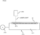
- the external force applied in the carbide layer formation step S20 may be applied by an adsorption power by a vacuum adsorption unit 270 illustrated in Fig. 5 .
- Absorption by the vacuum adsorption unit 270 may be set, for example, to 30 cmHg or more, and as an example, may be set to 30 cmHg or more and 60 cmcmHg or less.
- the vacuum adsorption unit 270 supports the front-surface electrode-equipped silicon carbide base 51, and includes a placement table 271 and a suction unit 272.
- the placement table 271 includes a plurality of suction holes 273 in a front surface thereof.
- the suction unit 272 includes a suction pump which applies, through the suction holes 273, a suction power to the silicon carbide wafer 10 placed on the placement table 271.
- the placement table 271 includes a hollow portion having a hollow shape in order to transmit the suction power from the suction unit 272 to the suction holes 273.
- the plurality of suction holes 273 may be successively provided in a line along the first direction, or may be successively provided in a line along the second direction perpendicular to the first direction. In addition, the plurality of suction holes 273 may not be provided in a line, but be placed on the surface of the placement table 271 concentrically at equal intervals. In a case where the plurality of suction holes 273 is successively provided in a line along the first direction, the plurality of suction holes 273 may be successively provided in parallel at intervals corresponding to the above-described "movement interval G", for example, intervals 0.5 to 2 times as long as the "movement interval G".
- the metal layer 21 formed in the metal layer formation step S25 may be a layer including titanium and molybdenum.
- the metal layer 21 may include only titanium, only molybdenum, or only titanium and molybdenum.
- the expression “only titanium” also means a case where a component other than titanium is included at an impurity level.
- the expression “only molybdenum” also means a case where a component other than molybdenum is included at an impurity level.
- the carbide layer 20 is formed by titanium carbide
- the carbide layer 20 is formed by molybdenum carbide.
- Green laser may be used as the laser light used in the carbide layer formation step S20.
- Output of the laser light may be set to 0.5 W or more at 10 kHZ, and for example, may be set to 0.5 W or more and 1.0 W or less.
- a total energy amount of laser may be set, for example, to 0.7 J/cm 2 or more, and for example, may be set to 0.7 J/cm 2 or more and 1.4 J/cm 2 or less.
- a laser scan speed may be set, for example, to 200 mm/sec or more, and for example, may be set to 200 mm/sec or more and 300 mm/sec or less.
- the silicon carbide semiconductor device 100 manufactured by the method for manufacturing the silicon carbide semiconductor device 100 according to the embodiment may include the silicon carbide wafer 10, the front-surface electrode 30 provided on the front surface side of the silicon carbide wafer 10, the carbide layer 20 provided on the back surface of the silicon carbide wafer 10 which has been thinned, and the back-surface electrode 40 provided on the back surface side of the carbide layer 20.
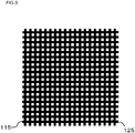
- the carbide layer 20 may include, as illustrated in Fig. 9 , a high-density portion 115 having high carbide density and a low-density portion 125 having low carbide density.
- the high-density portion 115 may be provided along two different directions which are in-plane directions of the carbide layer 20.
- An example of the two different directions includes, as illustrated in Fig. 9 , two directions which are perpendicular to each other in a plane of the silicon carbide wafer 10.
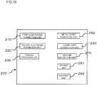
- a device used in the method for manufacturing the silicon carbide semiconductor device 100 according to the embodiment, as illustrated in the block diagram in Fig. 10 as an example, a device can be used which includes a first electrode formation unit 210, a thinning processing unit 230, a metal layer formation unit 250, an external force applying unit (in the embodiment, the vacuum adsorption unit 270), a laser light irradiation unit 260, and a second electrode formation unit 220.
- the first electrode formation unit 210 forms the front-surface electrode 30 on the front surface side of the silicon carbide wafer 10.
- the thinning processing unit 230 thins the silicon carbide wafer 10 by reducing the thickness of the silicon carbide wafer 10 from the back surface side thereof.
- the metal layer formation unit 250 provides the metal layer 21 on the back surface of the silicon carbide wafer 10 which has been thinned.
- the external force applying unit applies an external force such that the silicon carbide wafer 10 and the metal layer 21 are planarized.
- the laser light irradiation unit 260 irradiates the metal layer 21, to which the external force is being applied by the external force applying unit, with laser light to form the carbide layer 20 obtained by a reaction with carbon in the silicon carbide wafer, on the back surface side of the metal layer 21.
- the second electrode formation unit 220 forms the back-surface electrode 40 on the back surface side of the carbide layer 20.
- the external force is applied to the silicon carbide wafer 10.
- the manufacturing device 200 may include a drying unit 281 and a washing unit 282.
- the drying unit 281 performs the first drying step S22 and the second drying step S29 illustrated in Fig.2 .
- the washing unit 282 performs the first washing step S21 and the second washing step S28 illustrated in Fig.2 .
- first electrode formation unit 210 and the second electrode formation unit 220 those already known as a device for forming electrodes can be used.
- the first electrode formation unit 210 and the second electrode formation unit 220 may be devices different from each other, or may be devices the same as each other.
- a grinding device for grinding and reducing the thickness of the silicon carbide wafer 10 may be used, or a reactor for reducing the thickness of the silicon carbide wafer 10 with a chemical reaction may be used.
- a deposition device for depositing the metal layer 21 may be used, or a sputtering device for providing the metal layer 21 by performing sputtering may be used.
- the external force applying unit As the external force applying unit, the vacuum adsorption unit 270 described above, a pressing unit 290 used in a second embodiment, and the like can be used.
- the drying unit 281 for example, a spin dryer and the like can be used.
- the washing unit 282 a conventionally known wafer washing device can be used.
- the embodiment it is possible to eliminate or reduce warpage of the thinned silicon carbide wafer 10 by irradiating the metal layer 21 with laser light to form, not a silicide layer but the carbide layer 20, while applying an external force such that the silicon carbide wafer 10 and the metal layer 21 are planarized. Consequently, unlike the conventional technique provided by WO2012/049792 , it is possible to eliminate or reduce warpage of the thinned silicon carbide wafer 10 by a simple technique without removing an affected layer.
- the low-density portion and the high-density portion can be formed in a definite pattern in a plane of the silicon carbide wafer 10 (see Fig. 9 ).
- the carbide layer 20 can be surely formed on the silicon carbide wafer 10.
- a highly pure carbide layer 20 can be surely formed. As a result, it is possible to more surely eliminate or reduce warpage of the thinned silicon carbide wafer 10.
- the external force applied in the carbide layer formation step S20 has been applied by the adsorption power generated by the vacuum adsorption unit 270.
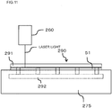
- the second embodiment adopts an aspect in which the external force applied in the carbide layer formation step S20 is applied by a pressing force by the pressing unit 290 made of a member which transmits laser light, as illustrated in Fig. 11 .
- a description will be given using an aspect in which the pressing unit 290 is used instead of the vacuum adsorption unit 270.
- the pressing unit 290 may be used together with the vacuum adsorption unit 270.
- the pressing unit 290 of the embodiment may be made of a material which transmits laser light.
- the pressing unit 290 may include a driving unit 292 and a pressing body 291.
- the driving unit 292 applies a pressing force.
- the pressing body 291 is connected to the driving unit 292 and transmits the pressing force from the driving unit to the silicon carbide wafer 10.
- the driving unit 292 may be connected to the placement table 275 or may be provided in the placement table 275.
- the pressing force may be applied to the silicon carbide wafer 10 by the driving unit 292 drawing the pressing body 291 toward the placement table 275.
- the driving unit 292 for example, those of hydraulic type can also be used.
- the pressing unit 290 is adopted as the external force applying unit, it is possible to physically planarize the silicon carbide wafer 10. Consequently, the carbide layer 20 can be formed while almost forcibly planarizing the silicon carbide wafer 10. As a result, it is possible to more surely eliminate or reduce warpage of the thinned silicon carbide wafer 10.
Landscapes
- Electrodes Of Semiconductors (AREA)
Applications Claiming Priority (1)
| Application Number | Priority Date | Filing Date | Title |
|---|---|---|---|
| PCT/JP2015/084828 WO2017098659A1 (ja) | 2015-12-11 | 2015-12-11 | 炭化珪素半導体装置の製造方法、半導体基体の製造方法、炭化珪素半導体装置及び炭化珪素半導体装置の製造装置 |
Publications (3)
| Publication Number | Publication Date |
|---|---|
| EP3389082A1 true EP3389082A1 (de) | 2018-10-17 |
| EP3389082A4 EP3389082A4 (de) | 2019-08-07 |
| EP3389082B1 EP3389082B1 (de) | 2020-10-28 |
Family
ID=57981556
Family Applications (1)
| Application Number | Title | Priority Date | Filing Date |
|---|---|---|---|
| EP15884168.4A Active EP3389082B1 (de) | 2015-12-11 | 2015-12-11 | Verfahren zur herstellung eines siliciumcarbidhalbleiterbauelements |
Country Status (6)
| Country | Link |
|---|---|
| US (1) | US9911811B2 (de) |
| EP (1) | EP3389082B1 (de) |
| JP (1) | JP6076548B1 (de) |
| CN (1) | CN107533961B (de) |
| TW (1) | TWI629715B (de) |
| WO (1) | WO2017098659A1 (de) |
Families Citing this family (5)
| Publication number | Priority date | Publication date | Assignee | Title |
|---|---|---|---|---|
| JPWO2018070263A1 (ja) * | 2016-10-13 | 2019-04-11 | 三菱電機株式会社 | 半導体装置の製造方法 |
| CN107649785A (zh) * | 2017-09-22 | 2018-02-02 | 北京世纪金光半导体有限公司 | 一种晶圆减薄方法及装置 |
| JP7187539B2 (ja) * | 2018-03-30 | 2022-12-12 | ローム株式会社 | 半導体装置 |
| JP7487739B2 (ja) * | 2019-07-17 | 2024-05-21 | 住友電気工業株式会社 | 半導体チップ及び半導体チップの製造方法 |
| CN113097069A (zh) * | 2021-03-31 | 2021-07-09 | 中国科学院微电子研究所 | 半导体器件的制备方法 |
Family Cites Families (13)
| Publication number | Priority date | Publication date | Assignee | Title |
|---|---|---|---|---|
| US7732301B1 (en) * | 2007-04-20 | 2010-06-08 | Pinnington Thomas Henry | Bonded intermediate substrate and method of making same |
| JP5369762B2 (ja) * | 2009-03-02 | 2013-12-18 | 株式会社デンソー | 炭化珪素半導体装置の製造方法 |
| JP5448652B2 (ja) * | 2009-09-01 | 2014-03-19 | 三菱電機株式会社 | 半導体装置およびその製造方法 |
| JP5550738B2 (ja) | 2010-10-15 | 2014-07-16 | 三菱電機株式会社 | 炭化珪素半導体素子の製造方法 |
| EP2698807B1 (de) * | 2011-04-11 | 2015-09-23 | Shindengen Electric Manufacturing Co., Ltd. | Verfahren zur herstellung eines halbleiterbauelements aus siliciumcarbid |
| JP5877005B2 (ja) * | 2011-07-29 | 2016-03-02 | 株式会社Screenホールディングス | 基板処理装置、基板保持装置、および、基板保持方法 |
| KR20140076566A (ko) * | 2011-10-07 | 2014-06-20 | 아사히 가라스 가부시키가이샤 | 탄화규소 단결정 기판 및 연마액 |
| JP5886005B2 (ja) | 2011-11-14 | 2016-03-16 | ルネサスエレクトロニクス株式会社 | 半導体装置の製造方法 |
| EP2913843A4 (de) * | 2012-10-23 | 2016-06-29 | Fuji Electric Co Ltd | Verfahren zur herstellung eines halbleiterbauelements |
| JP6197461B2 (ja) * | 2013-08-06 | 2017-09-20 | 住友電気工業株式会社 | 炭化珪素半導体基板およびその製造方法、ならびに炭化珪素半導体装置の製造方法 |
| JP6091406B2 (ja) * | 2013-12-16 | 2017-03-08 | 三菱電機株式会社 | 炭化珪素半導体装置の製造方法およびレーザアニール装置 |
| EP3134914B1 (de) * | 2014-04-23 | 2019-04-10 | United Silicon Carbide Inc. | Herstellung ohmscher kontakte auf halbleitern mit breiter bandlücke |
| JP6415946B2 (ja) * | 2014-11-26 | 2018-10-31 | 株式会社東芝 | 半導体装置の製造方法及び半導体装置 |
-
2015
- 2015-12-11 EP EP15884168.4A patent/EP3389082B1/de active Active
- 2015-12-11 CN CN201580007858.3A patent/CN107533961B/zh active Active
- 2015-12-11 JP JP2016537032A patent/JP6076548B1/ja active Active
- 2015-12-11 WO PCT/JP2015/084828 patent/WO2017098659A1/ja not_active Ceased
- 2015-12-11 US US15/121,002 patent/US9911811B2/en active Active
-
2016
- 2016-08-17 TW TW105126280A patent/TWI629715B/zh active
Also Published As
| Publication number | Publication date |
|---|---|
| JP6076548B1 (ja) | 2017-02-08 |
| CN107533961A (zh) | 2018-01-02 |
| TWI629715B (zh) | 2018-07-11 |
| JPWO2017098659A1 (ja) | 2017-12-07 |
| US9911811B2 (en) | 2018-03-06 |
| EP3389082B1 (de) | 2020-10-28 |
| WO2017098659A1 (ja) | 2017-06-15 |
| TW201721725A (zh) | 2017-06-16 |
| US20180019307A1 (en) | 2018-01-18 |
| EP3389082A4 (de) | 2019-08-07 |
| CN107533961B (zh) | 2020-08-21 |
Similar Documents
| Publication | Publication Date | Title |
|---|---|---|
| EP3389082B1 (de) | Verfahren zur herstellung eines siliciumcarbidhalbleiterbauelements | |
| US9136173B2 (en) | Singulation method for semiconductor die having a layer of material along one major surface | |
| US8664089B1 (en) | Semiconductor die singulation method | |
| US8048775B2 (en) | Process of forming ultra thin wafers having an edge support ring | |
| CN104752532B (zh) | 一种半导体器件的三维电极结构及其制备方法和应用 | |
| US9034733B2 (en) | Semiconductor die singulation method | |
| US11075070B2 (en) | Monocrystalline semiconductor wafer and method for producing a semiconductor wafer | |
| TW201234459A (en) | Semiconductor manufacturing apparatus and semiconductor substrate bonding method | |
| CN204424268U (zh) | 一种半导体器件的三维电极结构 | |
| EP4250338A3 (de) | Solarzellen-vorbereitungsverfahren | |
| KR20190047785A (ko) | 저차원 물질을 위한 표면처리 방법 | |
| RU2258978C2 (ru) | Способ изготовления полупроводниковых структур | |
| KR20110080336A (ko) | 척 핀을 구비한 기판 처리 장치 | |
| JP6500792B2 (ja) | エピタキシャルウェーハの品質評価方法および製造方法 | |
| JP5470766B2 (ja) | 半導体デバイスの製造方法 | |
| US20140151854A1 (en) | Method for Separating a Layer and a Chip Formed on a Layer | |
| CN111415898A (zh) | 晶圆组件及其制作方法 | |
| KR20130072014A (ko) | 에피텍셜 기판 및 패턴 형성 방법 |
Legal Events
| Date | Code | Title | Description |
|---|---|---|---|
| STAA | Information on the status of an ep patent application or granted ep patent |
Free format text: STATUS: THE INTERNATIONAL PUBLICATION HAS BEEN MADE |
|
| PUAI | Public reference made under article 153(3) epc to a published international application that has entered the european phase |
Free format text: ORIGINAL CODE: 0009012 |
|
| STAA | Information on the status of an ep patent application or granted ep patent |
Free format text: STATUS: REQUEST FOR EXAMINATION WAS MADE |
|
| 17P | Request for examination filed |
Effective date: 20180607 |
|
| AK | Designated contracting states |
Kind code of ref document: A1 Designated state(s): AL AT BE BG CH CY CZ DE DK EE ES FI FR GB GR HR HU IE IS IT LI LT LU LV MC MK MT NL NO PL PT RO RS SE SI SK SM TR |
|
| AX | Request for extension of the european patent |
Extension state: BA ME |
|
| DAV | Request for validation of the european patent (deleted) | ||
| DAX | Request for extension of the european patent (deleted) | ||
| A4 | Supplementary search report drawn up and despatched |
Effective date: 20190705 |
|
| RIC1 | Information provided on ipc code assigned before grant |
Ipc: H01L 21/268 20060101ALN20190701BHEP Ipc: H01L 21/28 20060101AFI20190701BHEP |
|
| GRAP | Despatch of communication of intention to grant a patent |
Free format text: ORIGINAL CODE: EPIDOSNIGR1 |
|
| STAA | Information on the status of an ep patent application or granted ep patent |
Free format text: STATUS: GRANT OF PATENT IS INTENDED |
|
| RIC1 | Information provided on ipc code assigned before grant |
Ipc: H01L 21/28 20060101AFI20200526BHEP Ipc: H01L 21/268 20060101ALN20200526BHEP |
|
| INTG | Intention to grant announced |
Effective date: 20200618 |
|
| GRAS | Grant fee paid |
Free format text: ORIGINAL CODE: EPIDOSNIGR3 |
|
| GRAA | (expected) grant |
Free format text: ORIGINAL CODE: 0009210 |
|
| STAA | Information on the status of an ep patent application or granted ep patent |
Free format text: STATUS: THE PATENT HAS BEEN GRANTED |
|
| AK | Designated contracting states |
Kind code of ref document: B1 Designated state(s): AL AT BE BG CH CY CZ DE DK EE ES FI FR GB GR HR HU IE IS IT LI LT LU LV MC MK MT NL NO PL PT RO RS SE SI SK SM TR |
|
| REG | Reference to a national code |
Ref country code: GB Ref legal event code: FG4D |
|
| RIN1 | Information on inventor provided before grant (corrected) |
Inventor name: FUKUDA, YUSUKE Inventor name: WATANABE, YOSHIYUKI |
|
| REG | Reference to a national code |
Ref country code: CH Ref legal event code: EP |
|
| REG | Reference to a national code |
Ref country code: DE Ref legal event code: R096 Ref document number: 602015061315 Country of ref document: DE |
|
| REG | Reference to a national code |
Ref country code: AT Ref legal event code: REF Ref document number: 1329069 Country of ref document: AT Kind code of ref document: T Effective date: 20201115 |
|
| REG | Reference to a national code |
Ref country code: IE Ref legal event code: FG4D |
|
| REG | Reference to a national code |
Ref country code: AT Ref legal event code: MK05 Ref document number: 1329069 Country of ref document: AT Kind code of ref document: T Effective date: 20201028 |
|
| REG | Reference to a national code |
Ref country code: NL Ref legal event code: MP Effective date: 20201028 |
|
| PG25 | Lapsed in a contracting state [announced via postgrant information from national office to epo] |
Ref country code: NO Free format text: LAPSE BECAUSE OF FAILURE TO SUBMIT A TRANSLATION OF THE DESCRIPTION OR TO PAY THE FEE WITHIN THE PRESCRIBED TIME-LIMIT Effective date: 20210128 Ref country code: RS Free format text: LAPSE BECAUSE OF FAILURE TO SUBMIT A TRANSLATION OF THE DESCRIPTION OR TO PAY THE FEE WITHIN THE PRESCRIBED TIME-LIMIT Effective date: 20201028 Ref country code: PT Free format text: LAPSE BECAUSE OF FAILURE TO SUBMIT A TRANSLATION OF THE DESCRIPTION OR TO PAY THE FEE WITHIN THE PRESCRIBED TIME-LIMIT Effective date: 20210301 Ref country code: FI Free format text: LAPSE BECAUSE OF FAILURE TO SUBMIT A TRANSLATION OF THE DESCRIPTION OR TO PAY THE FEE WITHIN THE PRESCRIBED TIME-LIMIT Effective date: 20201028 Ref country code: GR Free format text: LAPSE BECAUSE OF FAILURE TO SUBMIT A TRANSLATION OF THE DESCRIPTION OR TO PAY THE FEE WITHIN THE PRESCRIBED TIME-LIMIT Effective date: 20210129 |
|
| REG | Reference to a national code |
Ref country code: LT Ref legal event code: MG4D |
|
| PG25 | Lapsed in a contracting state [announced via postgrant information from national office to epo] |
Ref country code: ES Free format text: LAPSE BECAUSE OF FAILURE TO SUBMIT A TRANSLATION OF THE DESCRIPTION OR TO PAY THE FEE WITHIN THE PRESCRIBED TIME-LIMIT Effective date: 20201028 Ref country code: AT Free format text: LAPSE BECAUSE OF FAILURE TO SUBMIT A TRANSLATION OF THE DESCRIPTION OR TO PAY THE FEE WITHIN THE PRESCRIBED TIME-LIMIT Effective date: 20201028 Ref country code: BG Free format text: LAPSE BECAUSE OF FAILURE TO SUBMIT A TRANSLATION OF THE DESCRIPTION OR TO PAY THE FEE WITHIN THE PRESCRIBED TIME-LIMIT Effective date: 20210128 Ref country code: IS Free format text: LAPSE BECAUSE OF FAILURE TO SUBMIT A TRANSLATION OF THE DESCRIPTION OR TO PAY THE FEE WITHIN THE PRESCRIBED TIME-LIMIT Effective date: 20210228 Ref country code: LV Free format text: LAPSE BECAUSE OF FAILURE TO SUBMIT A TRANSLATION OF THE DESCRIPTION OR TO PAY THE FEE WITHIN THE PRESCRIBED TIME-LIMIT Effective date: 20201028 Ref country code: PL Free format text: LAPSE BECAUSE OF FAILURE TO SUBMIT A TRANSLATION OF THE DESCRIPTION OR TO PAY THE FEE WITHIN THE PRESCRIBED TIME-LIMIT Effective date: 20201028 Ref country code: SE Free format text: LAPSE BECAUSE OF FAILURE TO SUBMIT A TRANSLATION OF THE DESCRIPTION OR TO PAY THE FEE WITHIN THE PRESCRIBED TIME-LIMIT Effective date: 20201028 |
|
| PG25 | Lapsed in a contracting state [announced via postgrant information from national office to epo] |
Ref country code: NL Free format text: LAPSE BECAUSE OF FAILURE TO SUBMIT A TRANSLATION OF THE DESCRIPTION OR TO PAY THE FEE WITHIN THE PRESCRIBED TIME-LIMIT Effective date: 20201028 Ref country code: HR Free format text: LAPSE BECAUSE OF FAILURE TO SUBMIT A TRANSLATION OF THE DESCRIPTION OR TO PAY THE FEE WITHIN THE PRESCRIBED TIME-LIMIT Effective date: 20201028 |
|
| REG | Reference to a national code |
Ref country code: DE Ref legal event code: R097 Ref document number: 602015061315 Country of ref document: DE |
|
| PG25 | Lapsed in a contracting state [announced via postgrant information from national office to epo] |
Ref country code: SM Free format text: LAPSE BECAUSE OF FAILURE TO SUBMIT A TRANSLATION OF THE DESCRIPTION OR TO PAY THE FEE WITHIN THE PRESCRIBED TIME-LIMIT Effective date: 20201028 Ref country code: LT Free format text: LAPSE BECAUSE OF FAILURE TO SUBMIT A TRANSLATION OF THE DESCRIPTION OR TO PAY THE FEE WITHIN THE PRESCRIBED TIME-LIMIT Effective date: 20201028 Ref country code: CZ Free format text: LAPSE BECAUSE OF FAILURE TO SUBMIT A TRANSLATION OF THE DESCRIPTION OR TO PAY THE FEE WITHIN THE PRESCRIBED TIME-LIMIT Effective date: 20201028 Ref country code: EE Free format text: LAPSE BECAUSE OF FAILURE TO SUBMIT A TRANSLATION OF THE DESCRIPTION OR TO PAY THE FEE WITHIN THE PRESCRIBED TIME-LIMIT Effective date: 20201028 Ref country code: RO Free format text: LAPSE BECAUSE OF FAILURE TO SUBMIT A TRANSLATION OF THE DESCRIPTION OR TO PAY THE FEE WITHIN THE PRESCRIBED TIME-LIMIT Effective date: 20201028 Ref country code: SK Free format text: LAPSE BECAUSE OF FAILURE TO SUBMIT A TRANSLATION OF THE DESCRIPTION OR TO PAY THE FEE WITHIN THE PRESCRIBED TIME-LIMIT Effective date: 20201028 |
|
| REG | Reference to a national code |
Ref country code: CH Ref legal event code: PL |
|
| PG25 | Lapsed in a contracting state [announced via postgrant information from national office to epo] |
Ref country code: DK Free format text: LAPSE BECAUSE OF FAILURE TO SUBMIT A TRANSLATION OF THE DESCRIPTION OR TO PAY THE FEE WITHIN THE PRESCRIBED TIME-LIMIT Effective date: 20201028 Ref country code: MC Free format text: LAPSE BECAUSE OF FAILURE TO SUBMIT A TRANSLATION OF THE DESCRIPTION OR TO PAY THE FEE WITHIN THE PRESCRIBED TIME-LIMIT Effective date: 20201028 |
|
| PLBE | No opposition filed within time limit |
Free format text: ORIGINAL CODE: 0009261 |
|
| REG | Reference to a national code |
Ref country code: BE Ref legal event code: MM Effective date: 20201231 |
|
| STAA | Information on the status of an ep patent application or granted ep patent |
Free format text: STATUS: NO OPPOSITION FILED WITHIN TIME LIMIT |
|
| GBPC | Gb: european patent ceased through non-payment of renewal fee |
Effective date: 20210128 |
|
| 26N | No opposition filed |
Effective date: 20210729 |
|
| PG25 | Lapsed in a contracting state [announced via postgrant information from national office to epo] |
Ref country code: LU Free format text: LAPSE BECAUSE OF NON-PAYMENT OF DUE FEES Effective date: 20201211 Ref country code: FR Free format text: LAPSE BECAUSE OF NON-PAYMENT OF DUE FEES Effective date: 20201228 Ref country code: IE Free format text: LAPSE BECAUSE OF NON-PAYMENT OF DUE FEES Effective date: 20201211 Ref country code: AL Free format text: LAPSE BECAUSE OF FAILURE TO SUBMIT A TRANSLATION OF THE DESCRIPTION OR TO PAY THE FEE WITHIN THE PRESCRIBED TIME-LIMIT Effective date: 20201028 |
|
| PG25 | Lapsed in a contracting state [announced via postgrant information from national office to epo] |
Ref country code: GB Free format text: LAPSE BECAUSE OF NON-PAYMENT OF DUE FEES Effective date: 20210128 Ref country code: LI Free format text: LAPSE BECAUSE OF NON-PAYMENT OF DUE FEES Effective date: 20201231 Ref country code: CH Free format text: LAPSE BECAUSE OF NON-PAYMENT OF DUE FEES Effective date: 20201231 Ref country code: SI Free format text: LAPSE BECAUSE OF FAILURE TO SUBMIT A TRANSLATION OF THE DESCRIPTION OR TO PAY THE FEE WITHIN THE PRESCRIBED TIME-LIMIT Effective date: 20201028 |
|
| PG25 | Lapsed in a contracting state [announced via postgrant information from national office to epo] |
Ref country code: IS Free format text: LAPSE BECAUSE OF FAILURE TO SUBMIT A TRANSLATION OF THE DESCRIPTION OR TO PAY THE FEE WITHIN THE PRESCRIBED TIME-LIMIT Effective date: 20210228 Ref country code: TR Free format text: LAPSE BECAUSE OF FAILURE TO SUBMIT A TRANSLATION OF THE DESCRIPTION OR TO PAY THE FEE WITHIN THE PRESCRIBED TIME-LIMIT Effective date: 20201028 Ref country code: MT Free format text: LAPSE BECAUSE OF FAILURE TO SUBMIT A TRANSLATION OF THE DESCRIPTION OR TO PAY THE FEE WITHIN THE PRESCRIBED TIME-LIMIT Effective date: 20201028 Ref country code: CY Free format text: LAPSE BECAUSE OF FAILURE TO SUBMIT A TRANSLATION OF THE DESCRIPTION OR TO PAY THE FEE WITHIN THE PRESCRIBED TIME-LIMIT Effective date: 20201028 |
|
| PG25 | Lapsed in a contracting state [announced via postgrant information from national office to epo] |
Ref country code: MK Free format text: LAPSE BECAUSE OF FAILURE TO SUBMIT A TRANSLATION OF THE DESCRIPTION OR TO PAY THE FEE WITHIN THE PRESCRIBED TIME-LIMIT Effective date: 20201028 |
|
| PG25 | Lapsed in a contracting state [announced via postgrant information from national office to epo] |
Ref country code: BE Free format text: LAPSE BECAUSE OF NON-PAYMENT OF DUE FEES Effective date: 20201231 |
|
| REG | Reference to a national code |
Ref country code: DE Ref legal event code: R079 Ref document number: 602015061315 Country of ref document: DE Free format text: PREVIOUS MAIN CLASS: H01L0021280000 Ipc: H10D0064010000 |
|
| PGFP | Annual fee paid to national office [announced via postgrant information from national office to epo] |
Ref country code: DE Payment date: 20251211 Year of fee payment: 11 |
|
| PGFP | Annual fee paid to national office [announced via postgrant information from national office to epo] |
Ref country code: IT Payment date: 20251223 Year of fee payment: 11 |