EP3389134A1 - Dispositif électronique comprenant une antenne utilisant un matériau électriquement conducteur inclus dans un boîtier du dispositif électronique - Google Patents
Dispositif électronique comprenant une antenne utilisant un matériau électriquement conducteur inclus dans un boîtier du dispositif électronique Download PDFInfo
- Publication number
- EP3389134A1 EP3389134A1 EP18166669.4A EP18166669A EP3389134A1 EP 3389134 A1 EP3389134 A1 EP 3389134A1 EP 18166669 A EP18166669 A EP 18166669A EP 3389134 A1 EP3389134 A1 EP 3389134A1
- Authority
- EP
- European Patent Office
- Prior art keywords
- point
- electronic device
- plate
- ground
- antenna
- Prior art date
- Legal status (The legal status is an assumption and is not a legal conclusion. Google has not performed a legal analysis and makes no representation as to the accuracy of the status listed.)
- Ceased
Links
Images








Classifications
-
- H—ELECTRICITY
- H04—ELECTRIC COMMUNICATION TECHNIQUE
- H04M—TELEPHONIC COMMUNICATION
- H04M1/00—Substation equipment, e.g. for use by subscribers
- H04M1/02—Constructional features of telephone sets
- H04M1/0202—Portable telephone sets, e.g. cordless phones, mobile phones or bar type handsets
- H04M1/026—Details of the structure or mounting of specific components
-
- H—ELECTRICITY
- H01—ELECTRIC ELEMENTS
- H01Q—ANTENNAS, i.e. RADIO AERIALS
- H01Q1/00—Details of, or arrangements associated with, antennas
- H01Q1/12—Supports; Mounting means
- H01Q1/22—Supports; Mounting means by structural association with other equipment or articles
- H01Q1/24—Supports; Mounting means by structural association with other equipment or articles with receiving set
- H01Q1/241—Supports; Mounting means by structural association with other equipment or articles with receiving set used in mobile communications, e.g. GSM
- H01Q1/242—Supports; Mounting means by structural association with other equipment or articles with receiving set used in mobile communications, e.g. GSM specially adapted for hand-held use
- H01Q1/243—Supports; Mounting means by structural association with other equipment or articles with receiving set used in mobile communications, e.g. GSM specially adapted for hand-held use with built-in antennas
-
- H—ELECTRICITY
- H04—ELECTRIC COMMUNICATION TECHNIQUE
- H04M—TELEPHONIC COMMUNICATION
- H04M1/00—Substation equipment, e.g. for use by subscribers
- H04M1/02—Constructional features of telephone sets
- H04M1/0202—Portable telephone sets, e.g. cordless phones, mobile phones or bar type handsets
- H04M1/0249—Details of the mechanical connection between the housing parts or relating to the method of assembly
-
- H—ELECTRICITY
- H01—ELECTRIC ELEMENTS
- H01Q—ANTENNAS, i.e. RADIO AERIALS
- H01Q1/00—Details of, or arrangements associated with, antennas
- H01Q1/12—Supports; Mounting means
- H01Q1/22—Supports; Mounting means by structural association with other equipment or articles
- H01Q1/24—Supports; Mounting means by structural association with other equipment or articles with receiving set
-
- H—ELECTRICITY
- H01—ELECTRIC ELEMENTS
- H01Q—ANTENNAS, i.e. RADIO AERIALS
- H01Q1/00—Details of, or arrangements associated with, antennas
- H01Q1/36—Structural form of radiating elements, e.g. cone, spiral, umbrella; Particular materials used therewith
- H01Q1/38—Structural form of radiating elements, e.g. cone, spiral, umbrella; Particular materials used therewith formed by a conductive layer on an insulating support
-
- H—ELECTRICITY
- H01—ELECTRIC ELEMENTS
- H01Q—ANTENNAS, i.e. RADIO AERIALS
- H01Q1/00—Details of, or arrangements associated with, antennas
- H01Q1/42—Housings not intimately mechanically associated with radiating elements, e.g. radome
- H01Q1/422—Housings not intimately mechanically associated with radiating elements, e.g. radome comprising two or more layers of dielectric material
-
- H—ELECTRICITY
- H01—ELECTRIC ELEMENTS
- H01Q—ANTENNAS, i.e. RADIO AERIALS
- H01Q1/00—Details of, or arrangements associated with, antennas
- H01Q1/44—Details of, or arrangements associated with, antennas using equipment having another main function to serve additionally as an antenna, e.g. means for giving an antenna an aesthetic aspect
-
- H—ELECTRICITY
- H01—ELECTRIC ELEMENTS
- H01Q—ANTENNAS, i.e. RADIO AERIALS
- H01Q1/00—Details of, or arrangements associated with, antennas
- H01Q1/48—Earthing means; Earth screens; Counterpoises
-
- H—ELECTRICITY
- H01—ELECTRIC ELEMENTS
- H01Q—ANTENNAS, i.e. RADIO AERIALS
- H01Q9/00—Electrically-short antennas having dimensions not more than twice the operating wavelength and consisting of conductive active radiating elements
- H01Q9/04—Resonant antennas
- H01Q9/0407—Substantially flat resonant element parallel to ground plane, e.g. patch antenna
-
- H—ELECTRICITY
- H01—ELECTRIC ELEMENTS
- H01Q—ANTENNAS, i.e. RADIO AERIALS
- H01Q9/00—Electrically-short antennas having dimensions not more than twice the operating wavelength and consisting of conductive active radiating elements
- H01Q9/04—Resonant antennas
- H01Q9/0407—Substantially flat resonant element parallel to ground plane, e.g. patch antenna
- H01Q9/0421—Substantially flat resonant element parallel to ground plane, e.g. patch antenna with a shorting wall or a shorting pin at one end of the element
-
- H—ELECTRICITY
- H01—ELECTRIC ELEMENTS
- H01Q—ANTENNAS, i.e. RADIO AERIALS
- H01Q5/00—Arrangements for simultaneous operation of antennas on two or more different wavebands, e.g. dual-band or multi-band arrangements
- H01Q5/30—Arrangements for providing operation on different wavebands
- H01Q5/307—Individual or coupled radiating elements, each element being fed in an unspecified way
- H01Q5/314—Individual or coupled radiating elements, each element being fed in an unspecified way using frequency dependent circuits or components, e.g. trap circuits or capacitors
- H01Q5/328—Individual or coupled radiating elements, each element being fed in an unspecified way using frequency dependent circuits or components, e.g. trap circuits or capacitors between a radiating element and ground
-
- H—ELECTRICITY
- H04—ELECTRIC COMMUNICATION TECHNIQUE
- H04M—TELEPHONIC COMMUNICATION
- H04M2201/00—Electronic components, circuits, software, systems or apparatus used in telephone systems
- H04M2201/34—Microprocessors
-
- H—ELECTRICITY
- H04—ELECTRIC COMMUNICATION TECHNIQUE
- H04M—TELEPHONIC COMMUNICATION
- H04M2250/00—Details of telephonic subscriber devices
- H04M2250/06—Details of telephonic subscriber devices including a wireless LAN interface
-
- H—ELECTRICITY
- H04—ELECTRIC COMMUNICATION TECHNIQUE
- H04M—TELEPHONIC COMMUNICATION
- H04M2250/00—Details of telephonic subscriber devices
- H04M2250/22—Details of telephonic subscriber devices including a touch pad, a touch sensor or a touch detector
Definitions
- the disclosure relates to an antenna technology for utilizing a metal housing included in an electronic device.
- An electronic device such as a smartphone, a tablet, or the like may communicate with a network by using an antenna.
- the electronic device is using a metal material in a housing for the purpose of increasing strength (or rigidity) and improving a design.
- the electronic device may use a portion of a metal housing as an antenna.
- a feeding point and a ground point may be additionally implemented in the metal housing.
- a secondary process for deforming the housing may be required to implement a radiation structure.
- the mechanical strength of the metal housing may become weak or an assemble structure may become complicated.
- an aspect of the disclosure is to provide a method of using an original shape of a metal housing without any other process except for implementing a feeding point and a ground point in the metal housing.
- an electronic device in accordance with an aspect of the disclosure, includes a housing comprising a first plate, a second plate facing away from the first plate, and a side member surrounding a space between the first plate and the second plate, the second plate being formed of an electrically conductive material, the side member being formed of an electrically conductive material and including a first side extending in a first direction and having a first length, a second side extending in a second direction perpendicular to the first direction and having a second length shorter than the first length, a third side extending in parallel to the first side and having the first length, and a fourth side extending in parallel to the second side and having the second length, the side member further including an elongated slit extending from a first point in the first side to a second point in the third side along a portion of the first side, the second side, and a portion of the third side, and a non-conductive material filling the slit, a touchscreen display exposed through at least a portion of the first
- an electronic device in accordance with another aspect of the disclosure, includes a housing that includes a first plate, a second plate facing away from the first plate and including an electrically conductive material, and a side member surrounding a space between the first plate and the second plate, a display that is exposed through at least a portion of the first plate, a wireless communication circuit that feeds a first feeding point in the second plate, a ground plane that is electrically coupled to at least one first ground point in a first region of the second plate and a second ground point in a second region of the second plate, and at least one processor that is electrically connected to the display and the wireless communication circuit.
- the wireless communication circuit, the ground plane, and the at least one processor is positioned inside the housing.
- the side member is formed of an electrically conductive material.
- the side member includes a first side extending in a first direction and having a first length, a second side extending in a second direction perpendicular to the first direction and having a second length shorter than the first length, a third side extending in parallel to the first side and having the first length, and a fourth side extending in parallel to the second side and having the second length.
- the first feeding point is in a region between the second side and the at least one first ground point.
- the first feeding point is closer to the second side than the at least one first ground point is to the second side.
- the second ground point is closer in distance to the second side than the first feeding point and the at least one first ground point is to the second side, and is outside the region.
- the electronic device may transmit and receive signals in various frequency bands by using a plurality of feeding points and a plurality of ground points.
- the expressions "have,” “may have,” “include” and “comprise,” or “may include” and “may comprise” used herein indicate existence of corresponding features (e.g., elements such as numeric values, functions, operations, or components) but do not exclude presence of additional features.
- the expressions "A or B,” “at least one of A or/and B,” or “one or more of A or/and B,” and the like may include any and all combinations of one or more of the associated listed items.
- the term “A or B,” “at least one of A and B,” or “at least one of A or B” may refer to all of the case (1) where at least one A is included, the case (2) where at least one B is included, or the case (3) where both of at least one A and at least one B are included.
- first may be referred to as a second element
- a second element may be referred to as a first element
- the expression “configured to” used in this disclosure may be used as, for example, the expression “suitable for,” “having the capacity to,” “designed to,” “adapted to,” “made to,” or “capable of.”
- the term “configured to” must not mean only “specifically designed to” in hardware. Instead, the expression “a device configured to” may mean that the device is “capable of' operating together with another device or other components.
- a "processor configured to (or set to) perform A, B, and C” may mean a dedicated processor (e.g., an embedded processor) for performing a corresponding operation or a generic-purpose processor (e.g., a central processing unit (CPU) or an application processor (AP)) which performs corresponding operations by executing one or more software programs which are stored in a memory device.
- a dedicated processor e.g., an embedded processor
- a generic-purpose processor e.g., a central processing unit (CPU) or an application processor (AP)
- An electronic device may include at least one of, for example, smartphones, tablet personal computers (PCs), mobile phones, video telephones, electronic book readers, desktop PCs, laptop PCs, netbook computers, workstations, servers, personal digital assistants (PDAs), portable multimedia players (PMPs), Motion Picture Experts Group (MPEG-1 or MPEG-2) audio layer 3 (MP3) players, mobile medical devices, cameras, or wearable devices.
- PCs tablet personal computers
- PDAs personal digital assistants
- PMPs portable multimedia players
- MPEG-1 or MPEG-2 Motion Picture Experts Group
- MP3 Motion Picture Experts Group
- MPEG-1 or MPEG-2 Motion Picture Experts Group
- MP3 Motion Picture Experts Group
- MPEG-1 or MPEG-2 Motion Picture Experts Group
- MP3 Motion Picture Experts Group Audio layer 3
- the wearable device may include at least one of an accessory type (e.g., watches, rings, bracelets, anklets, necklaces, glasses, contact lens, or head-mounted-devices (HMDs), a fabric or garment-integrated type (e.g., an electronic apparel), a body-attached type (e.g., a skin pad or tattoos), or a bio-implantable type (e.g., an implantable circuit).
- an accessory type e.g., watches, rings, bracelets, anklets, necklaces, glasses, contact lens, or head-mounted-devices (HMDs)
- a fabric or garment-integrated type e.g., an electronic apparel
- a body-attached type e.g., a skin pad or tattoos
- a bio-implantable type e.g., an implantable circuit
- the electronic device may be a home appliance.
- the home appliances may include at least one of, for example, televisions (TVs), digital versatile disc (DVD) players, audios, refrigerators, air conditioners, cleaners, ovens, microwave ovens, washing machines, air cleaners, set-top boxes, home automation control panels, security control panels, TV boxes (e.g., Samsung HomeSyncTM, Apple TVTM, or Google TVTM), game consoles (e.g., XboxTM or PlayStationTM), electronic dictionaries, electronic keys, camcorders, electronic picture frames, and the like.
- TVs televisions
- DVD digital versatile disc
- an electronic device may include at least one of various medical devices (e.g., various portable medical measurement devices (e.g., a blood glucose monitoring device, a heartbeat measuring device, a blood pressure measuring device, a body temperature measuring device, and the like), a magnetic resonance angiography (MRA), a magnetic resonance imaging (MRI), a computed tomography (CT), scanners, and ultrasonic devices), navigation devices, Global Navigation Satellite System (GNSS), event data recorders (EDRs), flight data recorders (FDRs), vehicle infotainment devices, electronic equipment for vessels (e.g., navigation systems and gyrocompasses), avionics, security devices, head units for vehicles, industrial or home robots, automatic teller's machines (ATMs), points of sales (POSs) of stores, or internet of things (e.g., light bulbs, various sensors, electric or gas meters, sprinkler devices, fire alarms, thermostats, street lamps, toasters, exercise equipment, hot water tanks, heaters, boilers,
- the electronic device may include at least one of parts of furniture or buildings/structures, electronic boards, electronic signature receiving devices, projectors, or various measuring instruments (e.g., water meters, electricity meters, gas meters, or wave meters, and the like).
- the electronic device may be one of the above-described devices or a combination thereof.
- An electronic device according to an embodiment may be a flexible electronic device.
- an electronic device according to an embodiment of this disclosure may not be limited to the above-described electronic devices and may include other electronic devices and new electronic devices according to the development of technologies.
- the term "user” may refer to a person who uses an electronic device or may refer to a device (e.g., an artificial intelligence electronic device) that uses the electronic device.
- FIG. 1A is a view illustrating an electronic device according to an embodiment of the disclosure
- FIG. 1B illustrates a structure of an antenna according to an embodiment of the disclosure.
- an electronic device 100 may be surrounded by a housing.
- the housing of the electronic device 100 may include a first plate 110, a second plate 120 facing away from the first plate 110 and including an electrically conductive material, and a side member (130, 132, 134, 136) surrounding a space between the first plate 110 and the second plate 120.
- the first plate 110 may include a display 114 exposed through at least a portion of the first plate 110.
- the first plate 110 may be, for example, a front surface of the electronic device 100.
- the second plate 120 may include an electrically conductive material.
- the second plate 120 may be, for example, a rear surface of the electronic device 100.
- the second plate 120 may be, for example, at least a portion of a metal housing.
- the side member may include an electrically conductive material.
- the side member may be, for example, at least a portion of the metal housing.
- the side member may include a first side 130, a second side 132, a third side 134, and a fourth side 136.
- the first side 130 may extend in a first direction and may have a first length.
- the second side 132 may extend in a second direction perpendicular to the first direction and may have a second length shorter than the first length.
- the third side 134 may extend in parallel to the first side 130 and may have the first length.
- the fourth side 136 may extend in parallel to the second side 132 and may have the second length.
- At least one point in the second plate 120 may be electrically coupled to a printed circuit board in the electronic device 100.
- a first feeding point 122 may be electrically coupled to a wireless communication circuit
- at least one first ground point 124 and at least one second ground point 126 may be electrically coupled to a ground plane.
- the case where the number of the at least one second ground point 126 is "1" if the number of at least one first ground point 124 is "3" is illustrated in FIG. 1A as an exemplification.
- each of the at least one first ground point 124 and the at least one second ground point 126 may include one ground point or two or more ground points.
- a resonance frequency may vary with a distance between the first feeding point 122 and the at least one first ground point 124 or with a distance between the first feeding point 122 and the second side 132.
- the wireless communication circuit may be configured to feed the first feeding point 122 in the second plate 120.
- the second plate 120 may be fed in a direct feeding manner or in an indirect feeding manner.
- the ground plane may be electrically coupled to the at least one first ground point 124 in a first region of the second plate 120 and the at least one second ground point 126 in a second region of the second plate 120.
- the wireless communication circuit and the ground plane may be coupled to the second plate 120 through a connection member (e.g., a C-clip, a metal extension part, a screw, or a spring) extending from an antenna element.
- a connection member e.g., a C-clip, a metal extension part, a screw, or a spring
- the first feeding point 122 may be closer to the second side 132 than the at least one first ground point 124 (or than the at least one first ground point 124 is to the second side 132) and may be in a region between the second side 132 and the at least one first ground point 124.
- the at least one second ground point 126 may be closer in distance to the second side 132 than the first feeding point 122 and the at least one first ground point 124, and may be outside the region.
- a partial region of the second plate 120 may operate as an antenna.
- a partial region of the second plate 120 which is specified by locations of the first feeding point 122, the at least one first ground point 124, and the at least one second ground point 126, may operate as an antenna.
- the display 114 of the front surface of the electronic device 100 and the second plate 120 may operate as an antenna of a planar inverted F antenna (PIFA) type.
- PIFA planar inverted F antenna
- the electronic device 100 may feed the first feeding point 122 in the second plate 120, and the second plate 120 may be connected with a ground region of a printed circuit board 104 at the at least one first ground point 124. If power is supplied to the first feeding point 122, the second plate 120 may operate as an antenna of the PIFA type.
- spaces 102 of a given width may exist between the side member and the display 114.
- the spaces 102 of the given width may be a slot or a black matrix (BM).
- An electrical signal of an antenna may be radiated through the spaces 102.
- the spaces 102 may function as an opening through which the antenna radiates an electrical signal.
- a housing antenna of FIG. 1A according to an embodiment may radiate an electrical signal mainly through the space 102 of the left side.
- the wireless communication circuit of the electronic device 100 may be configured to feed a third feeding point in any region 112 of the first plate 110 other than the display 114.
- a conductive member 116 may be electrically coupled to the third feeding point.
- a separate antenna for wireless fidelity (Wi-Fi), Bluetooth (BT), or global positioning system (GPS) is mounted in the first plate 110, it may be possible to operate the antenna included in the second plate 120.
- FIG. 2 is a view for describing how a feeding point and a ground point are selected in a second plate, according to an embodiment of the disclosure.
- a resonance frequency of an antenna included in a second plate 210 may vary with locations of a feeding point and a ground point. For example, in the case where a distance from a second side 216 to at least one first ground point 214 is "D" and a distance from a first feeding point 212 to the at least one first ground point 214 is "G,” the electronic device 100 may transmit and receive a wireless signal of a frequency, which varies with the distances "G" and "D.”
- the second plate 210 may transmit and receive a signal of a frequency, which is differently determined depending on a location relationship of the second side 216, a feeding point, and a ground point.
- the at least one first ground point 214 may be at a point that is spaced apart from the second side 216 by a distance of " ⁇ /4.”
- " ⁇ " may be, as an example, a wavelength of a signal.
- the first feeding point 212 may be at a point that is spaced apart from the at least one first ground point 214 by a distance of " ⁇ /10.”
- locations of the at least one first ground point 214 and the first feeding point 212 may be determined in consideration of influence between the metal housing and a printed circuit board or any other part (or component) in the electronic device 100.
- the antenna included in the second plate 210 may transmit and receive a signal of 1.575 GHz.
- the antenna included in the second plate 210 may operate as a GPS antenna.
- the antenna included in the second plate 210 may transmit and receive a signal of 2.4 GHz.
- the antenna included in the second plate 210 may operate as a Wi-Fi antenna or a BT antenna.
- the antenna may be configured to transmit and receive a signal in a frequency range from 1.5 GHz to 2.4 GHz.
- FIG. 3 is a view for describing an operation of an antenna in the case where a second plate includes multiple feeding points, according to an embodiment of the disclosure.
- a second plate 310 (e.g., the second plate 120 of FIGS. 1A and 1B ) of an electronic device (e.g., the electronic device 100 of FIGS. 1A and 1B ) may include multiple feeding points.
- a wireless communication circuit of the electronic device may be configured to feed a second feeding point 316 in the second plate 310.
- a first feeding point 312 may be in a region between at least one first ground point 314 and the second feeding point 316.
- the second feeding point 316 may be closer in distance to a second side 318 than the first feeding point 312.
- the second plate 310 may transmit and receive a higher frequency when power is supplied through the second feeding point 316 than when power is supplied through the first feeding point 312.
- graph 320 is a graph for describing efficiency of an antenna included in the second plate 310.
- a resonance frequency is changed as the first feeding point 312 or the second feeding point 316 is selected as a feeding point.
- the antenna included in the second plate 310 may operate as an antenna of a multi-band.
- the antenna included in the second plate 310 may resonate at approximately 1.6 GHz. In this case, the radiation efficiency may be approximately -5dB. In the case where power is supplied through the second feeding point 316, the antenna included in the second plate 310 may resonate at approximately 2.4 GHz. In this case, the radiation efficiency may be approximately -5dB.
- the second plate 310 may operate as a GPS, BT, or Wi-Fi antenna through a multi-feed structure.
- FIG. 4 illustrates a schematic configuration of a switch associated with multiple feeding points of an antenna included in a second plate, according to an embodiment of the disclosure.
- an electronic device may include at least one switch 412.
- the at least one switch 412 may include a single-pole, double-throw (SP2T) switch, a single-pole, four-throw (SP4T) switch, or a micro electro-mechanical systems (MEMS) switch.
- the at least one switch 412 may include a tunable element or a tuner.
- the electronic device may selectively feed two or more feeding points by using the at least one switch 412.
- the electronic device may include the at least one switch 412 that is positioned inside a housing 418 and selectively couples a first feeding point 414 and a second feeding point 416.
- the housing 418 may be the second plate 120 of FIGS. 1A and 1B .
- the housing 418 may operates as a multi-band antenna by using the at least one switch 412.
- a feeding point is not limited to the first feeding point 414 and the second feeding point 416.
- the feeding point may include the determined feeding points.
- the housing 418 may include three or more feeding points.
- the electronic device may change a feeding location through a switching operation of the at least one switch 412, thus changing a resonance frequency.
- the housing 418 may operate as a GPS, BT, or Wi-Fi antenna through the switching operation of the at least one switch 412.
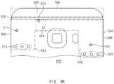
- FIGS. 5A to 5C are views illustrating an electronic device in the case where a plurality of antenna elements exists in a housing of an electronic device, according to an embodiment of the disclosure.
- a housing 500 of an electronic device may include a first antenna 510 and a second antenna 520, which are included in a second plate 540 (e.g., the second plate 120 of FIGS. 1A and 1B ).
- the first antenna 510 may be referenced as the antenna described with reference to FIGS. 1A , 1B , 2 , and 3 .
- the second plate 540 may further include a separate ground point in addition to a second ground point 512 (e.g., the at least one second ground point 126 of FIGS. 1A and 1B ).
- an isolation effect may be improved by adding a ground point between the antennas.
- a ground plane in the electronic device may be electrically coupled to a fourth ground point 514 in the second plate 540.
- the fourth ground point 514 may be near the second ground point 512.
- the addition of the fourth ground point 514 may make the isolation effect of the first antenna 510 and the second antenna 520 higher.
- a slit 530 may be formed in the housing 500 of the electronic device, and the slit 530 may be filled by a non-conductive material.
- the slit 530 may be in parallel to an extending line (e.g., a dotted line of a lower end of a second antenna 520 region) and may extend from a point in a first side 502 to a point in a third side 506.
- the slit 530 may be between a radiator of the second antenna 520 and points of the first antenna 510, which include a first feeding point 511, the second ground point 512, and the fourth ground point 514.
- the slit 530 may separate the radiator of the second antenna 520 and a radiator of the first antenna 510 together with the second ground point 512 and the fourth ground point 514.
- the radiator of the second antenna 520 may include at least a portion of a side member of a second side 504 of the housing 500, a portion of a side member extending from a point in the first side 502 to the second side 504, a portion of a side member extending from a point in the third side 506 to the second side 504, and a portion of the second plate 540 between the second side 504 and the slit 530.
- the first feeding point 511, one or more first ground point 513, the second ground point 512, and the fourth ground point 514, which are included in the first antenna 510 in the second plate 540, may be father in distance from the second side 504 than the slit 530.
- the housing 500 of the electronic device may include a third antenna 550.
- the third antenna 550 may include a second feeding point 551 and one or more fifth ground point 553.
- the third antenna 550 may share a ground point with the first antenna 510.
- the first antenna 510 and the second antenna 520 may be separated from the third antenna 550 by the shared ground point.
- the shared ground point may include the second ground point 512 and the fourth ground point 514.
- the second feeding point 551 of the third antenna 550 may be farther from the second side 504 than the first feeding point 511 of the first antenna 510.
- the third antenna 550 may resonate in a lower frequency band than the first antenna 510.
- the second plate 540 may include the first antenna 510 and the third antenna 550.
- the second plate 540 of FIG. 5B may include the first antenna 510 and the third antenna 550 except for the second antenna 520.
- the first antenna 510 and the third antenna 550 may share one or more of the second ground point 512 and the fourth ground point 514 and may transmit and receive signals having different frequencies.
- the second plate 540 may include nonmetal regions 520a and 520b or a metal region 520c.
- the first antenna 510 and the third antenna 550 may be disposed as illustrated in FIG. 5C .
- the first antenna 510 and the third antenna 550 may be in the metal region 520c.
- the nonmetal regions 510a and 510b may be formed in the case where a portion of the whole housing region is filled by a dielectric such as plastic.
- An antenna(s) may be mounted in the nonmetal regions 520a and 520b.
- the first antenna 510 may include a ground point for improving an isolation effect from an antenna mounted in the nonmetal region 520a.
- the third antenna 550 may include a ground point for improving an isolation effect from an antenna mounted in the nonmetal region 520b.
- FIG. 6 is a view for describing an isolation improvement effect between different antennas obtained by adding a ground point, according to an embodiment of the disclosure.
- graph 610 shows a result of verifying an isolation effect of the embodiment described with reference to FIGS. 5A to 5C through one experimental example. A description of FIG. 6 will be given by using the reference numerals of FIGS. 5A to 5C .
- the first antenna 510 included in the second plate 540 is a GPS antenna
- the second antenna 520 is a sub-antenna. Isolation between the first antenna 510 and the second antenna 520 is not well made in a band between approximately 1.7 GHz close to 1.575 GHz and approximately 1.8 GHz.
- 1.575 GHz may be a frequency of a GPS antenna, which belongs to a frequency band of the sub-antenna.
- the isolation effect was measured with respect to the band from 1.7 GHz to 1.8 GHz, which isolation is not well made.
- the following table shows a result of the graph 610 of FIG. 6 .
- the graph 610 of FIG. 6 indicates a transmission coefficient S21 associated with the frequency of 1.7 GHz.
- the graph 610 shows a result of measuring the transmission coefficient S21 by comparing case 612 where a ground point is absent from the second plate 540 and case 616 where two ground points are present in the second plate 540.
- the case 612 may correspond, for example, to the case where both the second ground point 512 and the fourth ground point 514 are absent from the second plate 540.
- Case 614 may correspond, for example, to the case where only the second ground point 512 is present in the second plate 540.
- the case 616 may correspond, for example, to the case where both the second ground point 512 and the fourth ground point 514 are present in the second plate 540.
- a peak value of the transmission coefficient S21 was observed as being -11.5 dB in the case 612, -13.1 dB in the case 614, and - 13.8 dB in the case 616. It is understood from the above description that the isolation effect between the first antenna 510 and the second antenna 520 is improved by increasing the number of ground points.
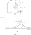
- FIG. 7 is a view for describing an operation of an antenna in the case where a second plate includes multiple ground points, according to an embodiment of the disclosure.
- a second plate 710 (e.g., the second plate 120 of FIGS. 1A and 1B ) of an electronic device (e.g., the electronic device 100 of FIGS. 1 A and 1B) may include multiple ground points.
- the second plate 710 may include a second ground point 716 and a third ground point 718.
- a ground plane in the electronic device may be electrically coupled to the third ground point 718 in the second plate 710.
- the third ground point 718 may be closer in distance to a second side 720 than a first feeding point 712 and at least one first ground point 714.
- the third ground point 718 may be in a region between the second side 720 and the at least one first ground point 714.
- a resonance frequency may change.
- a region "A" and a region "B” may operate as a radiator of an antenna.
- the region "B" may operate as a radiator of an antenna.
- a resonant frequency may be changed as a region of an antenna is changed.
- a graph 730 is a graph for describing efficiency of an antenna included in the second plate 710 in the case where the second ground point 716 or the third ground point 718 is a ground point.
- a line 732 indicates a graph corresponding to the case where the second ground point 716 is a ground point
- a line 734 indicates a graph corresponding to the case where the third ground point 718 is a ground point.
- a resonance frequency is changed as the second ground point 716 or the third ground point 718 is selected as a ground point.
- a resonance frequency may become higher.
- the regions "A" and "B" may be used as an antenna region, and a distance from the first feeding point 712 to the second side 720 are concerned in resonance.
- the region “B" may be used as an antenna region, and a distance from the first feeding point 712 to a boundary line of the region "B" is concerned in resonance.
- a resonant frequency may become higher as a resonance distance become shorter.
- the electronic device may include a switch that is selectively connected with the second ground point 716 or the third ground point 718.
- the electronic device may change a resonance frequency through a switching operation of the switch.
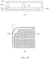
- FIG. 8 is a view illustrating structures of slits that are capable of being included in an electronic device, according to various embodiments of the disclosure.
- a side member of a housing of an electronic device 800 may include a slit extending along a region of at least one side.
- a slit included in a side member of a lower end of the electronic device 800 is illustrated in FIG. 8 , but a slit may be included in a side member of an upper end of the electronic device.
- a second plate (e.g., the second plate 120 of FIGS. 1 A and 1B) of the housing may be spaced apart from a portion of a side member of the housing by the slit.
- a plurality of antennas may be formed in the housing.
- partial regions or all regions of the plurality of antennas may be spaced apart from each other depending on a shape of the slit.
- the plurality of antennas may operate as different antennas.
- the plurality of antennas may operate as a primary antenna element and a secondary antenna element, which are used to transmit the same electrical signal.
- the plurality of antennas may include a plurality of primary antennas and a plurality of secondary antennas depending on a target frequency. The primary antennas and the secondary antennas may be used to transmit different electrical signals corresponding to respective frequencies.
- the one antenna element and the other antenna element may be electrically coupled to each other, thereby improving the performance of radiation of an antenna.
- the performance of radiation of an antenna (e.g., the first antenna 510 of FIG. 5A or 5B ) included in a second plate may be reduced by any other antenna element.
- any other antenna element separated by the slit and the antenna (e.g., the first antenna 510 of FIG. 5A or 5B ) included in the second plate may be electrically coupled to each other. Since a current is induced in the other antenna element, the overall performance of radiation of the antenna may be improved.
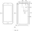
- FIG. 9 is a view illustrating an electronic device according to another embodiment of the disclosure.
- an electronic device 900 (e.g., the electronic device 100 of FIGS. 1A and 1B ) according to an embodiment may include a housing that includes a first plate 910, a second plate 920 facing away from the first plate 910, a side member surrounding a space between the first plate 910 and the second plate 920.
- the second plate 920 may include an electrically conductive material.
- the side member may include an electrically conductive material.
- the side member may include a first side 930 extending in a first direction and having a first length, a second side 932 extending in a second direction perpendicular to the first direction and having a second length shorter than the first length, a third side 934 extending in parallel to the first side 930 and having the first length, and a fourth side 936 extending in parallel to the second side 932 and having the second length.
- the side member of the electronic device 900 may further include an elongated slit 944 extending from a first point in the first side 930 to a second point in the third side 934 along a portion of the first side 930, the second side 932, and a portion of the third side 934, and a non-conductive material filling the elongated slit 944.
- the elongated slit 944 may make separation of a rear surface and a side surface of the second plate 920 better.
- the elongated slit 944 may be formed in various shapes.
- the elongated slit 944 may be formed in the slit shape described with reference to FIG. 8 .
- the electronic device 900 may include a touchscreen display that is exposed through at least a portion of the first plate 910, and a wireless communication circuit that is positioned inside the housing and is electrically coupled to a third point 928 and a fourth point 922 in the second plate 920.
- the electronic device 900 may include a ground plane that is positioned in the housing in parallel to the second plate 920 and is electrically coupled to at least one fifth point 924 and a sixth point 926 in the second plate 920.
- the third point 928 may be closer to the second side 932 than the sixth point 926.
- the sixth point 926 may be closer to the second side 932 than the fourth point 922 and the at least one fifth point 924, the third point 928 may be closer to the second side 932 than the sixth point 926, and the fourth point 922 may be closer to the second side 932 than the at least one fifth point 924.
- the electronic device 900 may include at least one processor that is positioned inside the housing and is electrically connected to the touchscreen display and the wireless communication circuit.
- a partial region of the second plate 920 may operate as a radiator of an antenna that uses the third point 928 and the fourth point 922 as a feeding point and the at least one fifth point 924 and the sixth point 926 as a ground point.
- the third point 928 or the fourth point 922 may be selectively fed, and thus, the antenna may transmit and receive different frequencies based at least partially on a feeding point.
- the fourth point 922 may be in a region between the third point 928 and the at least one fifth point 924 when viewed from above the second plate 920.
- the sixth point 926 may be outside the region.
- An antenna region in the second plate 920 may be specified based on locations of the third point 928 to the sixth point 926.
- FIG. 10 is a view illustrating an electronic device according to another embodiment of the disclosure.
- a housing of an electronic device 1000 may include a plurality of antenna elements.
- the electronic device 1000 may further include a switching element that is positioned inside the housing and is electrically coupled to a seventh point 1050 near a fourth side 1036.
- the seventh point 1050 may be a feeding point associated with an antenna 1052.
- the electronic device 1000 may control feeding the seventh point 1050 through the switching element.
- the housing may include an antenna 1042 extending from a first side 1030 of the housing to a second side 1032 and a third side 1034 or the antenna 1052 extending from the first side 1030 of the housing to the fourth side 1036 and the third side 1034.
- the antenna 1042 may be a sub-antenna
- the antenna 1052 may be a main antenna.
- an isolation effect of the antenna 1042 and an antenna included in a second plate 1020, which faces away from a first plate 1010, may be improved by a slit 1044.
- the electronic device 1000 may further include a switching element that is positioned inside the housing and is electrically coupled to an eighth point 1040, which is closer to the second side 1032 than a third point 1028.
- the eighth point 1040 may be a feeding point associated with the antenna 1042.
- the electronic device 1000 may control feeding the eighth point 1040 through the switching element.
- a fourth point 1022 may be in a region between the eighth point 1040 and at least one fifth point 1024 when viewed from above the second plate 1020.
- a sixth point 1026 may be outside the region.
- FIG. 11 illustrates an electronic device in a network environment system, according to various embodiments of the disclosure.
- an electronic device 1101, a first electronic device 1102, a second electronic device 1104, or a server 1106 may be connected each other over a network 1162 or a short range communication 1164.
- the electronic device 1101 may include a bus 1110, a processor 1120, a memory 1130, an input/output interface 1150, a display 1160, and a communication interface 1170.
- the electronic device 1101 may not include at least one of the above-described elements or may further include other element(s).
- the bus 1110 may interconnect the processor 1120, the memory 1130, the input/output interface 1150, the display 1160, and the communication interface 1170 and may include a circuit for conveying communications (e.g., a control message and/or data) among the above-described elements.
- communications e.g., a control message and/or data
- the processor 1120 may include one or more of a CPU, an AP, or a communication processor (CP). For example, the processor 1120 may perform an arithmetic operation or data processing associated with control and/or communication of at least other elements of the electronic device 1101.
- CP communication processor
- the memory 1130 may include a volatile and/or nonvolatile memory.
- the memory 1130 may store commands or data associated with at least one other element(s) of the electronic device 1101.
- the memory 1130 may store software and/or a program 1140.
- the program 1140 may include, for example, a kernel 1141, a middleware 1143, an application programming interface (API) 1145, and/or an application program (or "an application") 1147. At least a part of the kernel 1141, the middleware 1143, or the API 1145 may be referred to as an "operating system (OS)".
- OS operating system
- the kernel 1141 may control or manage system resources (e.g., the bus 1110, the processor 1120, the memory 1130, and the like) that are used to execute operations or functions of other programs (e.g., the middleware 1143, the API 1145, and the application program 1147). Furthermore, the kernel 1141 may provide an interface that allows the middleware 1143, the API 1145, or the application program 1147 to access discrete elements of the electronic device 1101 so as to control or manage system resources.
- system resources e.g., the bus 1110, the processor 1120, the memory 1130, and the like
- other programs e.g., the middleware 1143, the API 1145, and the application program 1147.
- the kernel 1141 may provide an interface that allows the middleware 1143, the API 1145, or the application program 1147 to access discrete elements of the electronic device 1101 so as to control or manage system resources.
- the middleware 1143 may perform, for example, a mediation role such that the API 1145 or the application program 1147 communicates with the kernel 1141 to exchange data.
- the middleware 1143 may process task requests received from the application program 1147 according to a priority. For example, the middleware 1143 may assign the priority, which makes it possible to use a system resource (e.g., the bus 1110, the processor 1120, the memory 1130, or the like) of the electronic device 1101, to at least one of the application program 1147. For example, the middleware 1143 may process the one or more task requests according to the priority assigned to the at least one, which makes it possible to perform scheduling or load balancing on the one or more task requests.
- a system resource e.g., the bus 1110, the processor 1120, the memory 1130, or the like
- the API 1145 may be, for example, an interface through which the application program 1147 controls a function provided by the kernel 1141 or the middleware 1143, and may include, for example, at least one interface or function (e.g., an instruction) for a file control, a window control, image processing, a character control, or the like.
- interface or function e.g., an instruction
- the input/output interface 1150 may play a role, for example, of an interface which transmits a command or data input from a user or another external device, to other element(s) of the electronic device 1101. Furthermore, the input/output interface 1150 may output a command or data, received from other element(s) of the electronic device 1101, to a user or another external device.
- the display 1160 may include, for example, a liquid crystal display (LCD), a light-emitting diode (LED) display, an organic LED (OLED) display, an MEMS display, or an electronic paper display.
- the display 1160 may display, for example, various contents (e.g., a text, an image, a video, an icon, a symbol, and the like) to a user.
- the display 1160 may include a touch screen and may receive, for example, a touch, gesture, proximity, or hovering input using an electronic pen or a part of a user's body.
- the communication interface 1170 may establish communication between the electronic device 1101 and an external device (e.g., the first electronic device 1102, the second electronic device 1104, or the server 1106).
- the communication interface 1170 may be connected to the network 1162 over wireless communication or wired communication to communicate with the external device (e.g., the second electronic device 1104 or the server 1106).
- the wireless communication may use at least one of, for example, long-term evolution (LTE), LTE advanced (LTE-A), code division multiple access (CDMA), wideband CDMA (WCDMA), universal mobile telecommunications system (UMTS), wireless broadband (WiBro), global system for mobile communications (GSM), or the like, as cellular communication protocol.
- LTE long-term evolution
- LTE advanced LTE advanced
- CDMA code division multiple access
- WCDMA wideband CDMA
- UMTS universal mobile telecommunications system
- WiBro wireless broadband
- GSM global system for mobile communications
- the wireless communication may include, for example, the short range communication 1164.
- the short range communication 1164 may include at least one of Wi-Fi, BT, near field communication (NFC), magnetic stripe transmission (MST), a GNSS, or the like.
- the MST may generate a pulse in response to transmission data using an electromagnetic signal, and the pulse may generate a magnetic field signal.
- the electronic device 1101 may transfer the magnetic field signal to point of sale (POS), and the POS may detect the magnetic field signal using a MST reader.
- the POS may recover the data by converting the detected magnetic field signal to an electrical signal.
- the GNSS may include at least one of, for example, a GPS, a global navigation satellite system (Glonass), a Beidou navigation satellite system (hereinafter referred to as "Beidou”), or an European global satellite-based navigation system (hereinafter referred to as "Galileo”) based on an available region, a bandwidth, or the like.
- GPS global navigation satellite system
- GNSS Beidou navigation satellite system
- Galileo European global satellite-based navigation system
- the wired communication may include at least one of, for example, a universal serial bus (USB), a high definition multimedia interface (HDMI), a recommended standard-232 (RS-232), a plain old telephone service (POTS), or the like.
- the network 1162 may include at least one of telecommunications networks, for example, a computer network (e.g., local area network (LAN) or wide area network (WAN)), an Internet, or a telephone network.
- LAN local area network
- WAN wide area network
- Each of the first and second electronic devices 1102 and 1104 may be a device of which the type is different from or the same as that of the electronic device 1101.
- the server 1106 may include a group of one or more servers. According to various embodiments, all or a portion of operations that the electronic device 1101 will perform may be executed by another or plural electronic devices (e.g., the first electronic device 1102, the second electronic device 1104 or the server 1106).
- the electronic device 1101 may not perform the function or the service internally, but, alternatively additionally, it may request at least a portion of a function associated with the electronic device 1101 from another device (e.g., the first electronic device 1102 or the second electronic device 1104 or the server 1106).
- the other electronic device may execute the requested function or additional function and may transmit the execution result to the electronic device 1101.
- the electronic device 1101 may provide the requested function or service using the received result or may additionally process the received result to provide the requested function or service.
- cloud computing, distributed computing, or client-server computing may be used.
- FIG. 12 illustrates a block diagram of an electronic device, according to various embodiments of the disclosure.
- an electronic device 1201 may include, for example, all or a part of the electronic device 1101 illustrated in FIG. 11 .
- the electronic device 1201 may include one or more processors (e.g., an AP) 1210, a communication module 1220, a subscriber identification module 1224, a memory 1230, a sensor module 1240, an input device 1250, a display 1260, an interface 1270, an audio module 1280, a camera module 1291, a power management module 1295, a battery 1296, an indicator 1297, and a motor 1298.
- processors e.g., an AP
- a communication module 1220 e.g., a communication module 1220, a subscriber identification module 1224, a memory 1230, a sensor module 1240, an input device 1250, a display 1260, an interface 1270, an audio module 1280, a camera module 1291, a power management module 1295, a battery 1296, an indicator 1297, and a motor 1298.
- the one or more processors 1210 may drive, for example, an OS or an application to control a plurality of hardware or software elements connected to the one or more processors 1210 and may process and compute a variety of data.
- the one or more processors 1210 may be implemented with a system on chip (SoC).
- SoC system on chip
- the one or more processors 1210 may further include a graphic processing unit (GPU) and/or an image signal processor (ISP).
- the one or more processors 1210 may include at least a part (e.g., a cellular module 1221) of elements illustrated in FIG. 12 .
- the one or more processors 1210 may load a command or data, which is received from at least one of other elements (e.g., a nonvolatile memory), into a volatile memory and process the loaded command or data.
- the one or more processors 1210 may store a variety of data in the nonvolatile memory.
- the communication module 1220 may be configured the same as or similar to the communication interface 1170 of FIG. 11 .
- the communication module 1220 may include the cellular module 1221, a Wi-Fi module 1223, a BT module 1225, a GNSS module 1227 (e.g., a GPS module, a Glonass module, a Beidou module, or a Galileo module), an NFC module 1228, and a radio frequency (RF) module 1229.
- a GNSS module 1227 e.g., a GPS module, a Glonass module, a Beidou module, or a Galileo module
- RF radio frequency
- the cellular module 1221 may provide, for example, voice communication, video communication, a character service, an Internet service, or the like over a communication network. According to an embodiment, the cellular module 1221 may perform discrimination and authentication of the electronic device 1201 within a communication network by using the subscriber identification module (e.g., a subscriber identification module (SIM) card) 1224. According to an embodiment, the cellular module 1221 may perform at least a portion of functions that the one or more processors 1210 provides. According to an embodiment, the cellular module 1221 may include a CP.
- SIM subscriber identification module
- Each of the Wi-Fi module 1223, the BT module 1225, the GNSS module 1227, or the NFC module 1228 may include a processor for processing data exchanged through a corresponding module, for example.
- at least a part (e.g., two or more) of the cellular module 1221, the Wi-Fi module 1223, the BT module 1225, the GNSS module 1227, or the NFC module 1228 may be included within one integrated circuit (IC) or an IC package.
- IC integrated circuit
- the RF module 1229 may transmit and receive a communication signal (e.g., an RF signal).
- the RF module 1229 may include a transceiver, a power amplifier module (PAM), a frequency filter, a low noise amplifier (LNA), an antenna, or the like.
- PAM power amplifier module
- LNA low noise amplifier
- at least one of the cellular module 1221, the Wi-Fi module 1223, the BT module 1225, the GNSS module 1227, or the NFC module 1228 may transmit and receive an RF signal through a separate RF module.
- the subscriber identification module 1224 may include, for example, a card and/or embedded SIM that includes a subscriber identification module and may include unique identify information (e.g., integrated circuit card identifier (ICCID)) or subscriber information (e.g., integrated mobile subscriber identity (IMSI)).
- ICCID integrated circuit card identifier
- IMSI integrated mobile subscriber identity
- the memory 1230 may include an internal memory 1232 or an external memory 1234.
- the internal memory 1232 may include at least one of a volatile memory (e.g., a dynamic random access memory (DRAM), a static RAM (SRAM), a synchronous DRAM (SDRAM), or the like), a nonvolatile memory (e.g., a one-time programmable read only memory (OTPROM), a programmable ROM (PROM), an erasable and programmable ROM (EPROM), an electrically erasable and programmable ROM (EEPROM), a mask ROM, a flash ROM, a flash memory (e.g., a NAND flash memory or a NOR flash memory), or the like), a hard drive, or a solid state drive (SSD).
- a volatile memory e.g., a dynamic random access memory (DRAM), a static RAM (SRAM), a synchronous DRAM (SDRAM), or the like
- a nonvolatile memory e
- the external memory 1234 may further include a flash drive such as compact flash (CF), secure digital (SD), micro-SD), mini-SD), extreme digital (xD), a multimedia card (MMC), a memory stick, or the like.
- CF compact flash
- SD secure digital
- micro-SD micro-SD
- mini-SD mini-SD
- extreme digital xD
- MMC multimedia card
- the external memory 1234 may be operatively and/or physically connected to the electronic device 1201 through various interfaces.
- the sensor module 1240 may measure, for example, a physical quantity or may detect an operation state of the electronic device 1201.
- the sensor module 1240 may convert the measured or detected information to an electric signal.
- the sensor module 1240 may include at least one of a gesture sensor 1240A, a gyro sensor 1240B, a barometric pressure sensor 1240C, a magnetic sensor 1240D, an acceleration sensor 1240E, a grip sensor 1240F, a proximity sensor 1240G, a color sensor 1240H (e.g., red, green, blue (RGB) sensor), a biometric sensor 12401, a temperature/humidity sensor 1240J, an illuminance sensor 1240K, or a UV sensor 1240M.
- the sensor module 1240 may further include, for example, an E-nose sensor, an electromyography (EMG) sensor, an electroencephalogram (EEG) sensor, an electrocardiogram (ECG) sensor, an infrared (IR) sensor, an iris sensor, and/or a fingerprint sensor.
- the sensor module 1240 may further include a control circuit for controlling at least one or more sensors included therein.
- the electronic device 1201 may further include a processor that is a part of the one or more processors 1210 or independent of the one or more processors 1210 and is configured to control the sensor module 1240. The processor may control the sensor module 1240 while the one or more processors 1210 remains at a sleep state.
- the input device 1250 may include, for example, a touch panel 1252, a (digital) pen sensor 1254, a key 1256, or an ultrasonic input unit 1258.
- the touch panel 1252 may use at least one of capacitive, resistive, IR and ultrasonic detecting methods.
- the touch panel 1252 may further include a control circuit.
- the touch panel 1252 may further include a tactile layer to provide a tactile reaction to a user.
- the (digital) pen sensor 1254 may be, for example, a part of a touch panel or may include an additional sheet for recognition.
- the key 1256 may include, for example, a physical button, an optical key, a keypad, or the like.
- the ultrasonic input device 1258 may detect (or sense) an ultrasonic signal, which is generated from an input device, through a microphone (e.g., a microphone 1288) and may check data corresponding to the detected ultrasonic signal.
- the display 1260 may include a panel 1262, a hologram device 1264, or a projector 1266.
- the panel 1262 may be the same as or similar to the display 1160 illustrated in FIG. 11 .
- the panel 1262 may be implemented, for example, to be flexible, transparent or wearable.
- the panel 1262 and the touch panel 1252 may be integrated into a single module.
- the hologram device 1264 may display a stereoscopic image in a space using a light interference phenomenon.
- the projector 1266 may project light onto a screen so as to display an image.
- the screen may be arranged in the inside or the outside of the electronic device 1201.
- the display 1260 may further include a control circuit for controlling the panel 1262, the hologram device 1264, or the projector 1266.
- the interface 1270 may include, for example, an HDMI 1272, a USB 1274, an optical interface 1276, or a D-subminiature (D-sub) 1278.
- the interface 1270 may be included, for example, in the communication interface 1170 illustrated in FIG. 11 .
- the interface 1270 may include, for example, a mobile high definition link (MHL) interface, a SD card/ MMC interface, or an infrared data association (IrDA) standard interface.
- MHL mobile high definition link
- SD card/ MMC interface Secure Digital MultimediaCard association
- IrDA infrared data association
- the audio module 1280 may convert a sound and an electric signal in dual directions. At least a part of the audio module 1280 may be included, for example, in the input/output interface 1150 illustrated in FIG. 11 .
- the audio module 1280 may process, for example, sound information that is input or output through a speaker 1282, a receiver 1284, an earphone 1286, or the microphone 1288.
- the camera module 1291 may shoot a still image or a video.
- the camera module 1291 may include at least one or more image sensors (e.g., a front sensor or a rear sensor), a lens, an ISP, or a flash (e.g., an LED or a xenon lamp).
- the power management module 1295 may manage, for example, power of the electronic device 1201.
- a power management integrated circuit PMIC
- the PMIC may have a wired charging method and/or a wireless charging method.
- the wireless charging method may include, for example, a magnetic resonance method, a magnetic induction method or an electromagnetic method and may further include an additional circuit, for example, a coil loop, a resonant circuit, or a rectifier, and the like.
- the battery gauge may measure, for example, a remaining capacity of the battery 1296 and a voltage, current or temperature thereof while the battery is charged.
- the battery 1296 may include, for example, a rechargeable battery and/or a solar battery.
- the indicator 1297 may display a specific state of the electronic device 1201 or a part thereof (e.g., the one or more processors 1210), such as a booting state, a message state, a charging state, and the like.
- the motor 1298 may convert an electrical signal into a mechanical vibration and may generate the following effects: vibration, haptic, and the like.
- a processing device e.g., a GPU
- the processing device for supporting the mobile TV may process media data according to the standards of digital multimedia broadcasting (DMB), digital video broadcasting (DVB), MediaFloTM, or the like.
- Each of the above-mentioned elements of the electronic device according to various embodiments of the disclosure may be configured with one or more components, and the names of the elements may be changed according to the type of the electronic device.
- the electronic device may include at least one of the above-mentioned elements, and some elements may be omitted or other additional elements may be added.
- some of the elements of the electronic device according to various embodiments may be combined with each other so as to form one entity, so that the functions of the elements may be performed in the same manner as before the combination.
- FIG. 13 illustrates a block diagram of a program module, according to various embodiments of the disclosure.
- a program module 1310 may include an OS to control resources associated with an electronic device (e.g., the electronic device 1101), and/or diverse applications (e.g., the application program 1147) driven on the OS.
- the OS may be, for example, AndroidTM, iOSTM, WindowsTM, SymbianTM, or TizenTM.
- the program module 1310 may include a kernel 1320, a middleware 1330, an API 1360, and/or an application 1370. At least a portion of the program module 1310 may be preloaded on an electronic device or may be downloadable from an external electronic device (e.g., the first electronic device 1102, the second electronic device 1104, the server 1106, or the like).
- an external electronic device e.g., the first electronic device 1102, the second electronic device 1104, the server 1106, or the like.
- the kernel 1320 may include, for example, a system resource manager 1321 or a device driver 1323.
- the system resource manager 1321 may perform control, allocation, or retrieval of system resources.
- the system resource manager 1321 may include a process managing unit, a memory managing unit, or a file system managing unit.
- the device driver 1323 may include, for example, a display driver, a camera driver, a BT driver, a shared memory driver, a USB driver, a keypad driver, a Wi-Fi driver, an audio driver, or an inter-process communication (IPC) driver.
- IPC inter-process communication
- the middleware 1330 may provide, for example, a function that the application 1370 needs in common, or may provide diverse functions to the application 1370 through the API 1360 to allow the application 1370 to efficiently use limited system resources of the electronic device.
- the middleware 1330 e.g., the middleware 1143 may include at least one of a runtime library 1335, an application manager 1341, a window manager 1342, a multimedia manager 1343, a resource manager 1344, a power manager 1345, a database manager 1346, a package manager 1347, a connectivity manager 1348, a notification manager 1349, a location manager 1350, a graphic manager 1351, or a security manager 1352.
- the runtime library 1335 may include, for example, a library module that is used by a compiler to add a new function through a programming language while the application 1370 is being executed.
- the runtime library 1335 may perform input/output management, memory management, or capacities about arithmetic functions.
- the application manager 1341 may manage, for example, a life cycle of at least one application of the application 1370.
- the window manager 1342 may manage a graphic user interface (GUI) resource that is used in a screen.
- GUI graphic user interface
- the multimedia manager 1343 may identify a format necessary for playing diverse media files, and may perform encoding or decoding of media files by using a codec suitable for the format.
- the resource manager 1344 may manage resources such as a storage space, memory, or source code of at least one application of the application 1370.
- the power manager 1345 may operate, for example, with a basic input/output system (BIOS) to manage a battery or power, and may provide power information for an operation of an electronic device.
- the database manager 1346 may generate, search for, or modify database that is to be used in at least one application of the application 1370.
- the package manager 1347 may install or update an application that is distributed in the form of package file.
- the connectivity manager 1348 may manage, for example, wireless connection such as Wi-Fi or BT.
- the notification manager 1349 may display or notify an event such as arrival message, appointment, or proximity notification in a mode that does not disturb a user.
- the location manager 1350 may manage location information about an electronic device.
- the graphic manager 1351 may manage a graphic effect that is provided to a user, or manage a user interface relevant thereto.
- the security manager 1352 may provide a general security function necessary for system security, user authentication, or the like.
- the middleware 1330 may further include a telephony manager for managing a voice or video call function of the electronic device.
- the middleware 1330 may include a middleware module that combines diverse functions of the above-described elements.
- the middleware 1330 may provide a module specialized to each OS kind to provide differentiated functions. Additionally, the middleware 1330 may dynamically remove a part of the preexisting elements or may add new elements thereto.
- the API 1360 may be, for example, a set of programming functions and may be provided with a configuration that is variable depending on an OS. For example, in the case where an OS is AndroidTM or iOSTM, it may provide one API set per platform. In the case where an OS is TizenTM, it may provide two or more API sets per platform.
- the application 1370 may include, for example, one or more applications capable of providing functions for a home 1371, a dialer 1372, a short message service (SMS)/multimedia message service (MMS) 1373, an instant message (IM) 1374, a browser 1375, a camera 1376, an alarm 1377, a contact 1378, a voice dial 1379, an e-mail 1380, a calendar 1381, a media player 1382, an album 1383, or a timepiece 1384 or for offering health care (e.g., measuring an exercise quantity, blood sugar, or the like) or environment information (e.g., information of barometric pressure, humidity, temperature, or the like).
- health care e.g., measuring an exercise quantity, blood sugar, or the like
- environment information e.g., information of barometric pressure, humidity, temperature, or the like.
- the application 1370 may include an application (hereinafter referred to as "information exchanging application” for descriptive convenience) to support information exchange between an electronic device (e.g., the electronic device 1101) and an external electronic device (e.g., the first electronic device 1102 or the second electronic device 1104).
- the information exchanging application may include, for example, a notification relay application for transmitting specific information to an external electronic device, or a device management application for managing the external electronic device.
- the notification relay application may include a function of transmitting notification information, which arise from other applications (e.g., applications for SMS/MMS, e-mail, health care, or environmental information), to an external electronic device.
- the information exchanging application may receive, for example, notification information from an external electronic device and provide the notification information to a user.
- the device management application may manage (e.g., install, delete, or update), for example, at least one function (e.g., turn-on/turn-off of an external electronic device itself (or a part of elements) or adjustment of brightness (or resolution) of a display) of the external electronic device which communicates with the electronic device, an application running in the external electronic device, or a service (e.g., a call service, a message service, or the like) provided from the external electronic device.
- a function e.g., turn-on/turn-off of an external electronic device itself (or a part of elements) or adjustment of brightness (or resolution) of a display
- a service e.g., a call service, a message service, or the like
- the application 1370 may include an application (e.g., a health care application of a mobile medical device) that is assigned in accordance with an attribute of an external electronic device.
- the application 1370 may include an application that is received from an external electronic device (e.g., the first electronic device 1102, the second electronic device 1104, or the server 1106).
- the application 1370 may include a preloaded application or a third party application that is downloadable from a server.
- the names of elements of the program module 1310 according to the embodiment may be modifiable depending on kinds of OSs.
- At least a portion of the program module 1310 may be implemented by software, firmware, hardware, or a combination of two or more thereof. At least a portion of the program module 1310 may be implemented (e.g., executed), for example, by the processor (e.g., the one or more processors 1210). At least a portion of the program module 1310 may include, for example, modules, programs, routines, sets of instructions, processes, or the like for performing one or more functions.
- An electronic device may include a housing including a first plate (e.g., the first plate 910 of FIG. 9 ), a second plate (e.g., the second plate 920 of FIG. 9 ) facing away from the first plate, a side member surrounding a space between the first plate and the second plate, wherein the second plate is formed of an electrically conductive material, wherein the side member is formed of an electrically conductive material and includes a first side (e.g., the first side 930 of FIG. 9 ) extending in a first direction and having a first length, a second side (e.g., the second side 932 of FIG.
- a housing including a first plate (e.g., the first plate 910 of FIG. 9 ), a second plate (e.g., the second plate 920 of FIG. 9 ) facing away from the first plate, a side member surrounding a space between the first plate and the second plate, wherein the second plate is formed of an electrically conductive material, wherein the side member is formed of
- the side member further includes an elongated slit extending from a first point in the first side to a second point in the third side along a portion of the first side, the second side, and a portion of the third side, and a non-conductive material filling the slit, a touchscreen display exposed through at least a portion of the first plate, a wireless communication circuit positioned inside the housing and electrically coupled to a third point (e.g., the third point 928 of FIG. 9 ) and a fourth point (e.g., the fourth point 922 of FIG.
- a third point e.g., the third point 928 of FIG. 9
- a fourth point e.g., the fourth point 922 of FIG.
- the electronic device may further include a switching element positioned inside the housing and electrically connected to a seventh point (e.g., the seventh point 1050 of FIG. 10 ) near the fourth side.
- a switching element positioned inside the housing and electrically connected to a seventh point (e.g., the seventh point 1050 of FIG. 10 ) near the fourth side.
- the fourth point of the electronic device may be in a region between the third point and the at least one fifth point when viewed from above the second plate.
- the sixth point of the electronic device according to an embodiment may be outside the region.
- the electronic device may further include a switching element positioned inside the housing and electrically connected to an eighth point (e.g., the eighth point 1040 of FIG. 10 ) that is closer to the second side than the third point is to the second side.
- a switching element positioned inside the housing and electrically connected to an eighth point (e.g., the eighth point 1040 of FIG. 10 ) that is closer to the second side than the third point is to the second side.
- the fourth point of the electronic device may be in a region between the eighth point and the at least one fifth point when viewed from above the second plate.
- the sixth point of the electronic device according to an embodiment may be outside the region.
- the communication circuit of the electronic device may be configured to provide a wireless signal in a frequency range of 1.5 GHz to 2.4 GHz.
- An electronic device may include a housing including a first plate (e.g., the first plate 110 of FIGS. 1A and 1B ), a second plate (e.g., the second plate 120 of FIG. 1 ) facing away from the first plate and including an electrically conductive material, and a side member (e.g., 130, 132, 134, and 136 of FIGS. 1A and 1B ) surrounding a space between the first plate and the second plate, a display exposed through at least a portion of the first plate, a wireless communication circuit configured to feed a first feeding point (e.g., the first feeding point 122 of FIGS.
- a first feeding point e.g., the first feeding point 122 of FIGS.
- the second plate in the second plate, a ground plane electrically coupled to at least one first ground point (e.g., the at least one first ground point 124 of FIGS. 1A and 1B ) in a first region of the second plate and a second ground point (e.g., the at least one second ground point 126 of FIGS. 1A and 1B ) in a second region of the second plate, and at least one processor electrically connected to the display and the wireless communication circuit.
- the wireless communication circuit, the ground plane, and the processor may be positioned inside the housing.
- the side member may be formed of an electrically conductive material, and may include a first side (e.g., the first side 130 of FIGS.
- a second side e.g., the second side 132 of FIGS. 1A and 1B ) extending in a second direction perpendicular to the first direction and having a second length shorter than the first length
- a third side e.g., the third side 134 of FIGS. 1A and 1B
- a fourth side e.g., the fourth side 136 of FIGS. 1A and 1B ) extending in parallel to the second side and having the second length.
- the first feeding point may be in a region between the second side and the at least one first ground point, the first feeding point may be closer to the second side than the at least one first ground point is to the second side, and the second ground point may be closer in distance to the second side than the first feeding point and the at least one first ground point is to the second side, and may be outside the region.
- the wireless communication circuit of the electronic device may be configured to feed a second feeding point (e.g., the second feeding point 316 of FIG. 3 ) in the second plate, and the first feeding point may be in a region between the at least one first ground point and the second feeding point.
- a second feeding point e.g., the second feeding point 316 of FIG. 3
- the electronic device may further include a switch that is positioned inside the housing and is selectively connected with the first feeding point and the second feeding point.
- the at least one first ground point of the electronic device may be at a point that is spaced apart from the second side by a distance of ⁇ /4, and the first feeding point may be at a point that is spaced apart from the at least one first ground point by a distance of ⁇ /10.
- the ground plane of the electronic device may be electrically coupled to a third ground point (e.g., the third ground point 718 of FIG. 7 ) in the second plate, and the third ground point may be closer in distance to the second side than the first feeding point and the at least one first ground point is to the second side, and is inside the region.
- a third ground point e.g., the third ground point 718 of FIG. 7
- the electronic device may further include a switch that is positioned inside the housing and is selectively connected with the second ground point or the third ground point.
- the ground plane of the electronic device may be electrically coupled to a fourth ground point in the second plate, and the fourth ground point may be near the second ground point.
- the electronic device may further include a first antenna including a portion of the side member extending from a point in the first side to a point in the third side along a portion of the first side, the second side, and a portion of the third side, and a portion of the second plate from the second side to a line that extends from the point in the first side to the point in the third side along the second plate.
- the first feeding point, the second ground point, and the fourth ground point may be farther in distance from the second side than the extending line is from the second side.
- the electronic device may further include a slit (e.g., the slit 530 of FIGS. 5A and 5B ) extending in parallel to the extending line along the second plate from the point in the first side to the point in the third side, and a non-conductive material filling the slit.
- the slit may be between the first antenna, and the first feeding point and the second ground point.
- the wireless communication circuit of the electronic device may be configured to feed a third feeding point that is in a region of the first plate except for the display.
- the electronic device may further include a conductive member electrically coupled to the third feeding point.
- the electronic device may further include a space between the side member and the display (e.g., the display 114 of FIG. 1 A) .
- module used in this disclosure may represent, for example, a unit including one or more combinations of hardware, software and firmware.
- the term “module” may be interchangeably used with the terms “unit”, “logic”, “logical block”, “component” and “circuit”.
- the “module” may be a minimum unit of an integrated component or may be a part thereof.
- the “module” may be a minimum unit for performing one or more functions or a part thereof.
- the “module” may be implemented mechanically or electronically.
- the “module” may include at least one of an application-specific IC (ASIC) chip, a field-programmable gate array (FPGA), and a programmable-logic device for performing some operations, which are known or will be developed.
- ASIC application-specific IC
- FPGA field-programmable gate array
- At least a part of an apparatus (e.g., modules or functions thereof) or a method (e.g., operations) may be, for example, implemented by instructions stored in a computer-readable storage media in the form of a program module.
- the instruction when executed by a processor (e.g., the processor 1120), may cause the one or more processors to perform a function corresponding to the instruction.
- the computer-readable storage media for example, may be the memory 1130.
- a computer-readable recording medium may include a hard disk, a floppy disk, a magnetic media (e.g., a magnetic tape), an optical media (e.g., a compact disc read only memory (CD-ROM) and a DVD, a magneto-optical media (e.g., a floptical disk)), and hardware devices (e.g., a read only memory (ROM), a random access memory (RAM), or a flash memory).
- the one or more instructions may contain a code made by a compiler or a code executable by an interpreter.
- the above hardware unit may be configured to operate via one or more software modules for performing an operation according to various embodiments, and vice versa.
- a module or a program module may include at least one of the above elements, or a part of the above elements may be omitted, or additional other elements may be further included.
- Operations performed by a module, a program module, or other elements according to various embodiments may be executed sequentially, in parallel, repeatedly, or in a heuristic method. In addition, some operations may be executed in different sequences or may be omitted. Alternatively, other operations may be added.
Landscapes
- Engineering & Computer Science (AREA)
- Computer Networks & Wireless Communication (AREA)
- Signal Processing (AREA)
- Support Of Aerials (AREA)
- Telephone Set Structure (AREA)
Applications Claiming Priority (1)
| Application Number | Priority Date | Filing Date | Title |
|---|---|---|---|
| KR1020170046244A KR102307730B1 (ko) | 2017-04-10 | 2017-04-10 | 전자 장치의 하우징에 포함된 도전성 물질을 이용하는 안테나를 포함하는 전자 장치 |
Publications (1)
| Publication Number | Publication Date |
|---|---|
| EP3389134A1 true EP3389134A1 (fr) | 2018-10-17 |
Family
ID=61965821
Family Applications (1)
| Application Number | Title | Priority Date | Filing Date |
|---|---|---|---|
| EP18166669.4A Ceased EP3389134A1 (fr) | 2017-04-10 | 2018-04-10 | Dispositif électronique comprenant une antenne utilisant un matériau électriquement conducteur inclus dans un boîtier du dispositif électronique |
Country Status (4)
| Country | Link |
|---|---|
| US (1) | US10665927B2 (fr) |
| EP (1) | EP3389134A1 (fr) |
| KR (1) | KR102307730B1 (fr) |
| CN (1) | CN108696607B (fr) |
Families Citing this family (10)
| Publication number | Priority date | Publication date | Assignee | Title |
|---|---|---|---|---|
| KR102482071B1 (ko) * | 2018-02-14 | 2022-12-28 | 삼성전자주식회사 | 다중 급전을 이용한 안테나 및 그것을 포함하는 전자 장치 |
| KR102662537B1 (ko) | 2019-05-10 | 2024-05-02 | 삼성전자 주식회사 | 이중 대역 안테나 및 그것을 포함하는 전자 장치 |
| KR102774920B1 (ko) * | 2019-12-27 | 2025-03-04 | 삼성전자주식회사 | 무선 통신 시스템에서 안테나의 최적 빔 구현을 위한 커버 장치 |
| CN112635967B (zh) * | 2020-12-07 | 2023-07-21 | Oppo广东移动通信有限公司 | 电子设备 |
| CN112635968B (zh) * | 2020-12-15 | 2023-12-26 | Oppo广东移动通信有限公司 | 电子设备 |
| US11835631B2 (en) | 2021-03-15 | 2023-12-05 | Qualcomm Incorporated | Devices and techniques for improving reception or compensating for attenuation of GNSS signals during water immersion activities |
| EP4451465A4 (fr) * | 2022-01-17 | 2025-04-16 | Samsung Electronics Co., Ltd | Dispositif électronique comprenant une antenne |
| USD1048001S1 (en) | 2022-02-28 | 2024-10-22 | Apple Inc. | Electronic device |
| TWI826074B (zh) * | 2022-10-25 | 2023-12-11 | 泓博無線通訊技術有限公司 | 用於筆記型電腦的切換式環天線模組 |
| USD1075748S1 (en) | 2023-04-28 | 2025-05-20 | Apple Inc. | Electronic device |
Citations (5)
| Publication number | Priority date | Publication date | Assignee | Title |
|---|---|---|---|---|
| US20110187611A1 (en) * | 2010-02-02 | 2011-08-04 | Laird Technologies Ab | Antenna Device For A Radio Communication Device |
| US20110254741A1 (en) * | 2010-04-16 | 2011-10-20 | Katsunori Ishimiya | Wireless communication device with housing member that functions as a radiating element of an antenna |
| WO2016154851A1 (fr) * | 2015-03-30 | 2016-10-06 | 华为技术有限公司 | Terminal |
| CN205828648U (zh) * | 2016-04-23 | 2016-12-21 | 深圳市威尔创通讯科技有限公司 | 全金属手机的三段式天线结构 |
| US20170033437A1 (en) * | 2015-07-31 | 2017-02-02 | AAC Technologies Pte. Ltd. | Mobile terminal device |
Family Cites Families (13)
| Publication number | Priority date | Publication date | Assignee | Title |
|---|---|---|---|---|
| US8872706B2 (en) * | 2010-11-05 | 2014-10-28 | Apple Inc. | Antenna system with receiver diversity and tunable matching circuit |
| US9024823B2 (en) * | 2011-05-27 | 2015-05-05 | Apple Inc. | Dynamically adjustable antenna supporting multiple antenna modes |
| US8890766B2 (en) | 2011-12-01 | 2014-11-18 | Sony Corporation | Low profile multi-band antennas and related wireless communications devices |
| US9287612B2 (en) * | 2012-11-16 | 2016-03-15 | Sony Mobile Communications Ab | Transparent antennas for wireless terminals |
| CN103633426B (zh) | 2013-12-06 | 2016-06-22 | 华为终端有限公司 | 天线结构和移动终端设备 |
| KR102151056B1 (ko) | 2014-04-09 | 2020-09-02 | 삼성전자주식회사 | 안테나 및 이를 구비한 전자 장치 |
| KR102177285B1 (ko) | 2014-09-01 | 2020-11-10 | 삼성전자주식회사 | 안테나 장치 및 그것을 포함하는 전자 장치 |
| US10096887B2 (en) | 2014-09-15 | 2018-10-09 | Blackberry Limited | Mobile device with tri-band antennas incorporated into a metal back side |
| US9608312B2 (en) | 2014-09-15 | 2017-03-28 | Blackberry Limited | Wideband antenna for mobile system with metal back cover |
| CN105517393A (zh) | 2014-09-24 | 2016-04-20 | 索尼公司 | 外壳以及包含该外壳的电子设备 |
| KR20160067541A (ko) * | 2014-12-04 | 2016-06-14 | 엘지전자 주식회사 | 안테나 모듈 및 이를 이용한 이동 단말기 |
| KR102176368B1 (ko) * | 2015-01-05 | 2020-11-09 | 엘지전자 주식회사 | 안테나 모듈 및 이를 구비하는 이동 단말기 |
| KR101643926B1 (ko) * | 2015-02-05 | 2016-07-29 | (주)파트론 | 안테나 구조물 |
-
2017
- 2017-04-10 KR KR1020170046244A patent/KR102307730B1/ko active Active
-
2018
- 2018-04-03 US US15/944,116 patent/US10665927B2/en active Active
- 2018-04-10 CN CN201810315393.3A patent/CN108696607B/zh active Active
- 2018-04-10 EP EP18166669.4A patent/EP3389134A1/fr not_active Ceased
Patent Citations (5)
| Publication number | Priority date | Publication date | Assignee | Title |
|---|---|---|---|---|
| US20110187611A1 (en) * | 2010-02-02 | 2011-08-04 | Laird Technologies Ab | Antenna Device For A Radio Communication Device |
| US20110254741A1 (en) * | 2010-04-16 | 2011-10-20 | Katsunori Ishimiya | Wireless communication device with housing member that functions as a radiating element of an antenna |
| WO2016154851A1 (fr) * | 2015-03-30 | 2016-10-06 | 华为技术有限公司 | Terminal |
| US20170033437A1 (en) * | 2015-07-31 | 2017-02-02 | AAC Technologies Pte. Ltd. | Mobile terminal device |
| CN205828648U (zh) * | 2016-04-23 | 2016-12-21 | 深圳市威尔创通讯科技有限公司 | 全金属手机的三段式天线结构 |
Also Published As
| Publication number | Publication date |
|---|---|
| KR20180114457A (ko) | 2018-10-18 |
| US20180294548A1 (en) | 2018-10-11 |
| CN108696607B (zh) | 2021-09-21 |
| CN108696607A (zh) | 2018-10-23 |
| US10665927B2 (en) | 2020-05-26 |
| KR102307730B1 (ko) | 2021-10-05 |
Similar Documents
| Publication | Publication Date | Title |
|---|---|---|
| US12126074B2 (en) | Electronic device including antenna | |
| US10608324B2 (en) | Electronic device comprising antenna | |
| US10826160B2 (en) | Electronic device comprising antenna | |
| US10608323B2 (en) | Electronic device including multi-band antenna | |
| US10446910B2 (en) | Electronic device with antenna | |
| US10665927B2 (en) | Electronic device comprising antenna which is using an electrically conductive material included in a housing of the electronic device | |
| US10916833B2 (en) | Antenna using coupling and electronic device including the same | |
| US11050136B2 (en) | Electronic device comprising antenna | |
| EP3522296B1 (fr) | Dispositif électronique comprenant une antenne | |
| US10707559B2 (en) | Electronic device including antenna | |
| EP3430681B1 (fr) | Dispositif électronique comprenant une antenne | |
| US11128038B2 (en) | Electronic device comprising antenna | |
| EP3340383B1 (fr) | Dispositif électronique comprenant une antenne | |
| US11069273B2 (en) | Display device for selectively outputting black data voltage in partial area and electronic device comprising display | |
| US11039401B2 (en) | Electronic device and method for adjusting electrical length of radiating portion |
Legal Events
| Date | Code | Title | Description |
|---|---|---|---|
| PUAI | Public reference made under article 153(3) epc to a published international application that has entered the european phase |
Free format text: ORIGINAL CODE: 0009012 |
|
| STAA | Information on the status of an ep patent application or granted ep patent |
Free format text: STATUS: THE APPLICATION HAS BEEN PUBLISHED |
|
| AK | Designated contracting states |
Kind code of ref document: A1 Designated state(s): AL AT BE BG CH CY CZ DE DK EE ES FI FR GB GR HR HU IE IS IT LI LT LU LV MC MK MT NL NO PL PT RO RS SE SI SK SM TR |
|
| AX | Request for extension of the european patent |
Extension state: BA ME |
|
| STAA | Information on the status of an ep patent application or granted ep patent |
Free format text: STATUS: REQUEST FOR EXAMINATION WAS MADE |
|
| 17P | Request for examination filed |
Effective date: 20181115 |
|
| RBV | Designated contracting states (corrected) |
Designated state(s): AL AT BE BG CH CY CZ DE DK EE ES FI FR GB GR HR HU IE IS IT LI LT LU LV MC MK MT NL NO PL PT RO RS SE SI SK SM TR |
|
| STAA | Information on the status of an ep patent application or granted ep patent |
Free format text: STATUS: EXAMINATION IS IN PROGRESS |
|
| 17Q | First examination report despatched |
Effective date: 20190328 |
|
| STAA | Information on the status of an ep patent application or granted ep patent |
Free format text: STATUS: THE APPLICATION HAS BEEN REFUSED |
|
| 18R | Application refused |
Effective date: 20230626 |