EP3392736B1 - System und verfahren zur dynamischen leistungsbegrenzung und lastverteilung für ein mehrknotensystem - Google Patents
System und verfahren zur dynamischen leistungsbegrenzung und lastverteilung für ein mehrknotensystem Download PDFInfo
- Publication number
- EP3392736B1 EP3392736B1 EP18162848.8A EP18162848A EP3392736B1 EP 3392736 B1 EP3392736 B1 EP 3392736B1 EP 18162848 A EP18162848 A EP 18162848A EP 3392736 B1 EP3392736 B1 EP 3392736B1
- Authority
- EP
- European Patent Office
- Prior art keywords
- power
- node
- nodes
- total
- balance
- Prior art date
- Legal status (The legal status is an assumption and is not a legal conclusion. Google has not performed a legal analysis and makes no representation as to the accuracy of the status listed.)
- Active
Links
Images



Classifications
-
- G—PHYSICS
- G06—COMPUTING OR CALCULATING; COUNTING
- G06F—ELECTRIC DIGITAL DATA PROCESSING
- G06F1/00—Details not covered by groups G06F3/00 - G06F13/00 and G06F21/00
- G06F1/26—Power supply means, e.g. regulation thereof
- G06F1/266—Arrangements to supply power to external peripherals either directly from the computer or under computer control, e.g. supply of power through the communication port, computer controlled power-strips
-
- G—PHYSICS
- G06—COMPUTING OR CALCULATING; COUNTING
- G06F—ELECTRIC DIGITAL DATA PROCESSING
- G06F9/00—Arrangements for program control, e.g. control units
- G06F9/06—Arrangements for program control, e.g. control units using stored programs, i.e. using an internal store of processing equipment to receive or retain programs
- G06F9/46—Multiprogramming arrangements
- G06F9/50—Allocation of resources, e.g. of the central processing unit [CPU]
- G06F9/5094—Allocation of resources, e.g. of the central processing unit [CPU] where the allocation takes into account power or heat criteria
-
- G—PHYSICS
- G06—COMPUTING OR CALCULATING; COUNTING
- G06F—ELECTRIC DIGITAL DATA PROCESSING
- G06F1/00—Details not covered by groups G06F3/00 - G06F13/00 and G06F21/00
- G06F1/26—Power supply means, e.g. regulation thereof
- G06F1/32—Means for saving power
- G06F1/3203—Power management, i.e. event-based initiation of a power-saving mode
-
- G—PHYSICS
- G06—COMPUTING OR CALCULATING; COUNTING
- G06F—ELECTRIC DIGITAL DATA PROCESSING
- G06F1/00—Details not covered by groups G06F3/00 - G06F13/00 and G06F21/00
- G06F1/26—Power supply means, e.g. regulation thereof
- G06F1/28—Supervision thereof, e.g. detecting power-supply failure by out of limits supervision
-
- G—PHYSICS
- G06—COMPUTING OR CALCULATING; COUNTING
- G06F—ELECTRIC DIGITAL DATA PROCESSING
- G06F1/00—Details not covered by groups G06F3/00 - G06F13/00 and G06F21/00
- G06F1/26—Power supply means, e.g. regulation thereof
-
- G—PHYSICS
- G06—COMPUTING OR CALCULATING; COUNTING
- G06F—ELECTRIC DIGITAL DATA PROCESSING
- G06F1/00—Details not covered by groups G06F3/00 - G06F13/00 and G06F21/00
- G06F1/26—Power supply means, e.g. regulation thereof
- G06F1/32—Means for saving power
- G06F1/3203—Power management, i.e. event-based initiation of a power-saving mode
- G06F1/3206—Monitoring of events, devices or parameters that trigger a change in power modality
-
- G—PHYSICS
- G06—COMPUTING OR CALCULATING; COUNTING
- G06F—ELECTRIC DIGITAL DATA PROCESSING
- G06F11/00—Error detection; Error correction; Monitoring
- G06F11/30—Monitoring
- G06F11/3058—Monitoring arrangements for monitoring environmental properties or parameters of the computing system or of the computing system component, e.g. monitoring of power, currents, temperature, humidity, position, vibrations
- G06F11/3062—Monitoring arrangements for monitoring environmental properties or parameters of the computing system or of the computing system component, e.g. monitoring of power, currents, temperature, humidity, position, vibrations where the monitored property is the power consumption
Definitions
- the present disclosure relates generally to system for power management in a multi-node system. More particularly, aspects of this disclosure relate to a system that manages power distribution in a multi-node system based on dynamic balancing of power to nodes.
- PSU power system unit
- the PSU provides power for multiple nodes such as cores that constitute a processing unit on a computer motherboard.
- another PSU is also connected to supply power to the nodes.
- the overall system may be designed so the total power consumption is below that certain level to avoid system failure if one of the PSUs fails.
- each PSU in such a system is configured to have enough power to allow operation of the multiple nodes at normal operation levels when the other PSU fails.
- Another known method to insure adequate power is to set a power limitation of each node as dividing the overall power consumption by the number of nodes and arrive at a set power level for each node.
- the system meets the target power levels by a software algorithm run by the chassis management controller.
- the controller is limited to the chassis management controller (CMC), but it could be baseboard management controller (BMC) or the controller of PSU.
- CMC chassis management controller
- BMC baseboard management controller
- the US 2015/177814 A1 discloses a computer-implemented method enabling rack-level predictive power capping and power budget allocation to processing nodes in a rack-based information handling system.
- a rack-level management controller receives node-level power-usage data and settings from several block controllers, including current power consumption and an initial power budget for each node.
- a power consumption profile is generated based on the power-usage data for each node.
- a total available system power of the information handling system is identified.
- a system power cap is determined based on the power consumption profiles and the total available system power.
- a current power budget is determined for each node based on an analysis of at least one of the power consumption profile, the initial power budget, the current power consumption, the system power cap, and the total available system power.
- a power subsystem regulates power budgeted and supplied to each node based on the power consumption profiles and the system power cap.
- the problem of the present invention is solved by a multi-node system according to the independent claim 1 and by a method of managing power in a system according to the independent claim 7.
- the dependent claims refer to advantageous further developments of the present invention. Embodiments which do not fall within the scope of the claims do not describe part of the present invention.
- One disclosed example is a multi-node system that dynamically allocates power.
- the system includes a plurality of nodes and a power source providing power to each of the nodes.
- a chassis management controller is coupled to the power source.
- the chassis management controller is operable to regulate the power from the power source to each of the nodes.
- the chassis management controller balances the power supplied to each node by determining a setting power for each node and a real power consumed for each node.
- the chassis management controller determines a next setting power for each node based on the real power and unused total power and total additional balance power for the plurality of nodes.
- the chassis management controller will provide the next setting power value to the baseboard management controller of each node.
- the baseboard management controller will regulate power consumption to key components such as the CPU or memory up to the next setting power value of the nodes.
- Another example is a method of managing power in a system including a plurality of nodes where each node consumes power.
- a setting power for each node and a real power consumed for each node is determined.
- a next setting power for each node is determined based on the real power and unused total power and total additional balance power for the plurality of nodes.
- the real power is regulated up to the next setting power value to each of the nodes.
- the power supply unit for allocating power to a plurality of nodes.
- the power supply unit includes a power supply circuit supplying power to each of the plurality of nodes.
- a chassis management controller regulates the power supply circuit.
- the chassis management controller is operative to determine the real power consumed by each of the nodes and determine the unused total power of all of the nodes.
- the chassis management controller determines additional balance power for each of the nodes.
- the chassis management controller determines the ratio of power usage for each of the nodes based on the real power consumed by the node and a setting power value for the node.
- the chassis management controller determines an add back balance power for each node based on the unused total power and the ratio of power usage.
- the chassis management controller determines a next setting power value for each node based on the real power consumed by the node, the additional balance power for the node and the add back balance power for the node.
- the chassis management controller will provide the next setting power value to the baseboard management controller of each node.
- the baseboard management controller will regulate key components power consumption up to the next setting power value of the nodes.
- FIG. 1 shows a block diagram of an example system 100 that supports multiple nodes and is thus a multi-node system.
- the system 100 includes a power supply unit (PSU) 102 that supplies power to the components on the motherboard 100.
- a backup power supply unit 108 identical to the power supply unit 102 may be provided for backup power.
- the system 100 includes multiple nodes such as nodes 130, 132, 134 and 136 in this example that constitute a multi-node system 140.
- Each of the nodes 130, 132, 134 and 136 is a motherboard and thus include a processor, a memory and a baseboard management controller. It is to be understood that the principles explained herein may be applied to power distribution for multi-node systems that have any number of nodes powered by one or more power supply units.
- the power consumption of the nodes 130, 132, 134 and 136 may be determined via current sensors 150, 152, 154 and 156 on the respective nodes 130, 132, 134 and 136.
- the outputs of the current sensors 150, 152, 154 and 156 are coupled to a chassis management controller 142 and may provide power consumption data for the chassis management controller 142 to allocate power to the nodes 130, 132, 134 and 136.
- the system 100 in FIG. 1 may be part of a computing system that includes multi-node motherboards and other boards that perform other functions such as memory devices or interface devices.
- the nodes 130, 132, 134 and 136 of the multi-node system 140 are powered by the power supply unit 102.
- the chassis management controller 142 may regulate the power supplied to the nodes 130, 132, 134 and 136 and optionally other components on the system 100.
- the chassis management controller 142 operates as a management controller and may include separate rewritable memory and permanent memory for application software.
- the chassis management controller 142 may also include communication interfaces that allows communication between the chassis management controller and a data bus such as a Power Management bus (PMbus) that may be coupled to a power controller of PSU.
- PMbus Power Management bus
- Another communication interfaces allow communication between chassis manager and a data bus such as a SMBus that may be coupled to BMC of MB.
- the chassis management controller 142 may receive performance data for multiple processors from the data bus for purposes such as network operation, administration, or trouble shooting.
- any suitable controller may be used for the chassis management controller 142.
- the functions of the chassis management controller 142 of monitoring and regulating power may be performed by one of the nodes such as the node 130 or as part of a baseboard management controller on one of the nodes or a power controller that may be part of the PSU 102.
- the process of distributing power between multiple nodes in a system such as the system 100 by the chassis management controller 142 in this example allows dynamic balancing of power between the multiple nodes.
- the multi-node system that may be operated with dynamic power balancing includes a total number of nodes, n, and each node includes a node number x that is from 1 to n.
- the four cores 130, 132, 134, and 136 of the system 100 in FIG. 1 may be designated as node 1, node 2, node 3 and node 4 respectively.
- a setting power (SP) for the system such as the system 100 is established.
- the setting power is the power value that is set to a certain power value to limit system power consumption.
- the cores of a processor such as the multi-node system 100 will decrease their operation rate to try to reach the setting power value for the node if power consumption is higher than the setting power.
- the setting power of each of the nodes is designated as SPx.
- the setting power for node 1 (SP1) could be 450 W.
- the real power of the system is designated as RP.
- the real power for each node is designated as RPx.
- the real power is the power value that the system reads from the current sensors of the system such as the current sensors 150, 152, 154 and 156 of the system 100.
- the real power for node 1 could be 380W indicating that the power consumed by the node is less than the setting power.
- the total power of the system is designated as TP.
- the total power of the system (TP) is determined by the total real power consumed by the n-node system (the sum of the real power of each node) in addition to the power of other boards and devices.
- the power of other boards and devices may be expressed as OP.
- the total power of the system (TP) may be measured by a current sensor of the power supply unit.
- the power of the other boards and devices (OP) may be determined by subtracting the total real power from the total power of the system.
- the total real power is determined by the controller such as the chassis management controller 142 based on the power data values read from the current sensors 150, 152, 154 and 156 on each of the respective nodes 130, 132, 134 and 136.
- the unused total power of the multi-node system is designated as UTP.
- the unused total power is determined by determining the total power consumption that may be afforded by the power supply unit such as the power supply unit 102 designated as MOP (Max Output Power of the PSU or a power value that is determined to be safe for long-time running of the system) and subtracting the system total power (TP).
- MOP Maximum Output Power of the PSU or a power value that is determined to be safe for long-time running of the system
- TP system total power
- the additional balance power for each node is designated as SBPx which is equivalent to the real power of the node multiplied by a coefficient y.
- SBPx yRPx for each node.
- the coefficient y is a value higher than 0 and lower than 1 and may be a constant value or a dynamic value.
- the coefficient y may be set at a relatively higher value to balance all available power between nodes but may be set at a relatively lower value to optimize power to certain high demand nodes while reducing power to low demand nodes.
- the additional balance power takes out a proportion designated as the y coefficient of node power before the power allocation process to constitute the power budget for balancing purposes.
- each of the setting power values for the nodes is reduced to provide unused total power for balancing purposes.
- the power reduced for each of the nodes is proportional to the load of each of the nodes. For example, a heavier loading node will supply more additional balance power. In some instances, a lighter loading node will not require full power, and thus the power budget may be arranged to supply more power to a node that requires more power reflecting available power from lighter loading nodes.
- TBP total balance power budget
- the degree of power usage for each of the nodes is designated as PUx, where the degree of power usage is the real power of the node (RPx) divided by the setting power of the node (SPx).
- the degree of power usage may indicate how much power is required for each node. If the degree of power usage is one or greater than one for a node, this indicates that the node requires the entire setting power or more power than the value of the setting power for the node. In this example, the degree of power usage for node 1 is below 1 and thus the node requires less than the setting power.
- the ratio of power usage for a node x in the system is designated as %(PUx) and may be determined by the power usage of the node divided by the total power usage of all the nodes.
- %(PUx) The ratio of power usage for a node is used to allocate the power budget reserved for system power balance.
- the higher the ratio of power usage for a node the more power is budgeted to the node by the chassis management controller 142.
- the balance power budget (ABP) for each node is designated as ABPx.
- the system also determines the next setting power for each of the nodes NSPx.
- the next setting power is stored in the memory of the controller such as the chassis management controller 142 and is used for determining power reallocation between the nodes.
- the chassis management controller 142 causes the baseboard management controller to allocate power to each of the nodes 130, 132, 134 and 136 in accordance with the next setting power.
- the change in power for each of the nodes 130, 132, 134 and 136 allows for dynamic power balancing based on the power needs of the nodes.
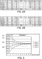
- FIG. 2A and FIG. 2B are tables that show the setting power, real power, additional balance power, degree of power usage, ratio of power usage, add balance power budget and the next setting power for each of the nodes 130, 132, 134 and 136 in the example motherboard 100 in FIG. 1 .
- the values in FIG. 2A and FIG. 2B assume a high power use scenario where each of the nodes 130, 132, 134 and 136 in FIG. 1 are drawing a large amount of power.
- the values in FIG. 2A-2B are determined by the chassis management controller 142 based on the power consumed by each of the nodes as measured by the power monitors 150, 152, 154 and 156.
- the unused total power UTP is zero.
- the coefficient y is 0.3 in this example and thus the additional balance power for each of the nodes is 0.3 of the real power of the node.
- the ratio of power usage for each of the nodes is 1 indicating that the real power is the same as the setting power.
- the power for node 1 is 500 W
- the power for node 2 is 400 W
- the power for node 3 is 300 W
- the power for node 4 is 200 W.
- the total balance power budget (TBP) is 420.
- TBP total balance power budget
- the total node power consumption is 1400 W
- the power of other board and devices (OP) is 200W. So total power consumption is 1600W, it is the same as the available power of 1600 W and the unused total power UTP is thus zero.
- FIG. 2B is a table showing the adjusted values for the nodes 130, 132, 134 and 136 after the above described power balancing process is performed by the chassis management controller 142.
- the setting power of the heaviest loaded nodes node 1 and node 2 have been reduced and the setting power of the less loaded nodes (nodes 3 and 4) have been increased.
- the next setting power of 455 from node 1 in the table in FIG. 2A is determined by taking the real power of 500 for node 1 and subtracting the additional balance power value (SBPx) of 150 and adding the balance power budget (ABPx) of 105 thus resulting in the next setting power of 455.
- SBPx additional balance power value
- ABSPx balance power budget
- the additional balance power value (SBPx) of 150 is obtained by multiplying the real power of node 1, 500 in this example, by the coefficient y, which is 0.3 in this example, resulting in the additional balance power value of 150.
- the balance power budget value of 105 is obtained by multiplying the total balance power budget of 420 by the ratio of power usage of 0.25 for node 1.
- next setting power values obtained in FIG. 2A are then used as the setting power values in the next iteration of the power balancing process as shown in FIG. 2B .
- the next setting power for the heavier load node 1 is further reduced to 423.5 while the next setting power for the lighter load node 4 is further increased to 276.5.
- the chassis management controller 142 may then perform the same power balancing power using the next setting power values in FIG. 2B .
- the iterative performance of this process allows the dynamic allocation of power to the nodes 130, 132, 134 and 136 in FIG. 1 .
- FIG. 3 is a graph that shows the real power values of each of the nodes 130, 132, 134 and 136 after performing the power balancing process described above ten times.
- the real power values for the nodes 130, 132, 134 and 136 are represented by lines 300, 302, 304 and 306 respectively.
- the system load balances as the real power values converge to 350 W for each of the nodes.
- FIGs. 4A, 4B and 4C are tables that show the setting power, real power, additional balance power, degree of power usage, ratio of power usage, add balance power budget and the next setting power for each of the nodes 130, 132, 134 and 136 in the example system 100 in FIG. 1 during the performance of the power balancing process described above.
- the first and third nodes 130 and 134 are subject to higher power requirements while the second and fourth nodes 132 and 136 are subject to lower power requirements.
- the coefficient y is 0.1 and thus the additional balance power for each of the nodes is 0.1 of the real power.
- the ratio of power usage for each of the node 1 and node 3 is 1 indicating that the real power is the same as the setting power and they have higher power requirements.
- the ratio of power usage for the node 2 and node 4 is 0.9, indicating that they have lower power requirements than node 1 and node 3.
- the setting power for node 1 is 500
- the setting power for node 2 is 500
- the setting power for node 3 is 300
- the setting power for node 4 is 300.
- the real power is 500 for node 1, 450 for node 2, 300 for node 3 and 270 for node 4.
- the total balance power budget (TBP) is 232.
- the total node power consumption is 1600W, and the power of other board and devices (OP) is 200W.
- the total power consumption is the same as the available power of 1800 and the unused total power UTP is zero.
- FIG. 4B is a table showing the adjusted values after the above described power balancing process is performed from the values in FIG. 4A .
- the setting power of the heaviest loaded nodes nodes 1 and node 3
- the setting power of the lighter loaded nodes nodes 2 and 4
- the next setting power of 511.1 from node 1 in the table in FIG. 4A is determined by taking the real power of 500 for node 1 and subtracting the additional balance power value (SBPx) of 50 and adding the balance power budget (ABPx) of 61.1 thus resulting in the next setting power of 511.1 for node 1.
- SBPx additional balance power value
- ABSPx balance power budget
- the additional balance power value (SBPx) of 50 is obtained by multiplying the real power of node 1, 500 in this example, by the coefficient y, which is 0.1 in this example, resulting in the additional balance power value of 50 for node 1.
- the balance power budget value of 61.1 is obtained by multiplying the total balance power budget of 232 by the ratio of power usage of 0.26 for node 1.
- next setting power values obtained in FIG. 4A are then used as the setting power values in the next iteration of the power balancing process as shown in FIG. 4B .
- the next setting power for the heavier load node 1 is further increased to 520.8.
- node 2 has a setting power of 459.9 in the table in FIG. 4B that is determined by taking the real power of 450 for node 2 as shown in FIG. 4A and subtracting the additional balance power value (SBPx) of 45 and adding the balance power budget (ABPx) of 54.9 thus resulting in the next setting power of 459.9 in FIG. 4B .
- the additional balance power value (SBPx) of 45 is obtained by multiplying the real power of node 2, 450 in this example, by the coefficient y, which is 0.1 in this example, resulting in the additional balance power value of 45.
- the balance power budget value of 54.9 is obtained by multiplying the total balance power budget of 232 by the ratio of power usage of 0.24 for node 2. As shown in FIG. 4B , the next setting power for the lighter load node 2 is further decreased to 433.5.
- FIG. 4C shows the power values for the nodes after the third iteration of the power balancing application is executed.
- the setting power for the higher power requirement nodes 1 and 3 has been increased from the values in FIG. 4B
- the setting power for the lower power requirement nodes 2 and 4 has been reduced from the values in FIG. 4B .
- FIG. 5 is a graph that shows the setting power values of each of the nodes 130, 132, 134 and 136 after performing the power balancing process 10 times from the initial values in the table in FIG. 4A .
- the setting power values for the nodes 130, 132, 134 and 136 are represented by lines 500, 502, 504 and 506 respectively.
- the system load balances power between the nodes allowing increased setting power for higher power requirement nodes such as node 1 represented by the line 500 and node 3 represented by line 504.
- the setting power is decreased for lower power requirement nodes such as the nodes 2 and 4 represented by lines 502 and 506.
- the coefficient y may be adjusted to optimize power balancing depending on the needs of the system.
- the coefficient y is set to 0.3 in order to allow all the nodes to achieve the same average power as all the nodes need more power.
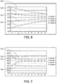
- FIG. 6 is a graph that shows the setting power values of each of the nodes 130, 132, 134 and 136 after performing the power balancing process described above ten times with the starting values in FIG. 2A .
- the setting power values for the nodes 130, 132, 134 and 136 are represented by lines 600, 602, 604 and 606 respectively when the coefficient y is set to 0.1.
- the system load balances at a slower rate thus showing a higher y value is more desirable to balance power when all the nodes need additional power.
- FIG. 7 is a graph that shows the setting power values of each of the nodes 130, 132, 134 and 136 after performing the power balancing process described above ten times with the starting values in FIG. 4A .
- the setting power values for the nodes 130, 132, 134 and 136 are represented by lines 700, 702, 704 and 706 respectively when the coefficient y is set to 0.3.
- the system allocates less power to the nodes that need more power thus showing a lower y value is more desirable to balance power when only some of the nodes need additional power.
- FIG. 8 shows a flow diagram of the algorithm executed by a management controller such as the chassis management controller 142 in FIG. 1 to dynamically distribute power to the nodes of a multi-node system.
- the flow diagram in FIG. 8 is representative of example machine readable instructions for a multi-node system such as the system 100 in FIG. 1 .
- the machine readable instructions comprise an algorithm for execution by: (a) a processor, (b) a controller, and/or (c) one or more other suitable processing device(s).
- the algorithm may be embodied in software stored on tangible media such as, for example, a flash memory, a CD-ROM, a floppy disk, a hard drive, a digital video (versatile) disk (DVD), or other memory devices, but persons of ordinary skill in the art will readily appreciate that the entire algorithm and/or parts thereof could alternatively be executed by a device other than a processor and/or embodied in firmware or dedicated hardware in a well-known manner (e.g., it may be implemented by an application specific integrated circuit (ASIC), a programmable logic device (PLD), a field programmable logic device (FPLD), a field programmable gate array (FPGA), discrete logic, etc.).
- ASIC application specific integrated circuit
- PLD programmable logic device
- FPLD field programmable logic device
- FPGA field programmable gate array
- any or all of the components of the interfaces could be implemented by software, hardware, and/or firmware.
- some or all of the machine readable instructions represented by the flowchart of FIG. 8 may be implemented manually.
- the example algorithm is described with reference to the flowcharts illustrated in FIG. 8 , persons of ordinary skill in the art will readily appreciate that many other methods of implementing the example machine readable instructions may alternatively be used.
- the order of execution of the blocks may be changed, and/or some of the blocks described may be changed, eliminated, or combined.
- the chassis management controller 142 first initiates the power balancing procedure (800).
- the power balancing procedure may be performed on a periodic basis for a multi-node system or may be initiated in response to a change in operation of one or more of the nodes.
- the chassis management controller 142 determines the unused total power by taking the overall power output of the power supply unit 102 (MOP) and subtracting the TP (802).
- the chassis management controller 142 determines the additional balance power for the system by adding the real power for each node multiplied by the coefficient y (804).
- the chassis management controller 142 determines the ratio of power usage for each of the nodes (806).
- the ratio of power usage for a node is determined by dividing the degree of power usage for a node PUx by the total degree of power usage for all the nodes, PU.
- the degree of power usage is determined by dividing the real power of the node (RPx) by the setting power of the node (SPx).
- the chassis management controller 142 then adds back the total balance power budget to each of the nodes by allocating the total balance power budget between the nodes (808).
- the added back total balance power for a node is determined by taking the total balance power budget (TBP) and multiplying it by the degree of power usage for the node (%(PUx)).
- the total balance power budget is determined by taking the unused total power (UTP) and adding the additional balance power determined from real power usage for each of the nodes multiplied by the coefficient y (yRPx).
- the chassis management controller 142 determines the next setting power for each node (NSPx) (810).
- the next setting power is determined by subtracting the additional balance power (SBPx) for the node from the real power for the node (RPx) and adding the total balance power for the node (ABPx).
- the chassis management controller 142 then regulates the power supply circuit 106 to supply real power up to the next setting power value to each of the nodes in the system. The process then loops back and rebalances power allocation according to the next setting power for each of the nodes.
- a component As used in this application, the terms “component,” “module,” “system,” or the like are generally intended to refer to a computer-related entity, either hardware (e.g., a circuit), a combination of hardware and software, software, or an entity related to an operational machine with one or more specific functionalities.
- a component may be, but is not limited to being, a process running on a processor (e.g., digital signal processor), a processor, an object, an executable, a thread of execution, a program, and/or a computer.
- a processor e.g., digital signal processor
- an application running on a controller and the controller can be a component.
- One or more components may reside within a process and/or thread of execution and a component may be localized on one computer and/or distributed between two or more computers.
- a “device” can come in the form of specially designed hardware; generalized hardware made specialized by the execution of software thereon that enables the hardware to perform specific function; software stored on a computer-readable medium; or a combination thereof.
- Computer-readable storage media can be any available storage media that can be accessed by the computer, is typically of a non-transitory nature, and can include both volatile and nonvolatile media, removable and non-removable media.
- Computer-readable storage media can be implemented in connection with any method or technology for storage of information such as computer-readable instructions, program modules, structured data, or unstructured data.
- Computer-readable storage media can include, but are not limited to, RAM, ROM, EEPROM, flash memory or other memory technology, CD-ROM, digital versatile disk (DVD) or other optical disk storage, magnetic cassettes, magnetic tape, magnetic disk storage or other magnetic storage devices, or other tangible and/or non-transitory media which can be used to store desired information.
- Computer-readable storage media can be accessed by one or more local or remote computing devices, e.g., via access requests, queries or other data retrieval protocols, for a variety of operations with respect to the information stored by the medium.
Landscapes
- Engineering & Computer Science (AREA)
- Theoretical Computer Science (AREA)
- General Engineering & Computer Science (AREA)
- Physics & Mathematics (AREA)
- General Physics & Mathematics (AREA)
- Software Systems (AREA)
- Computer Hardware Design (AREA)
- Power Sources (AREA)
- Supply And Distribution Of Alternating Current (AREA)
- Management, Administration, Business Operations System, And Electronic Commerce (AREA)
Claims (11)
- System mit mehreren Knoten, das zur dynamischen Zuweisung von Leistung betrieben werden kann, wobei das System aufweist:eine Vielzahl an Knoten (130, 132, 134 und 136), die Stromsensoren (150, 152, 154 und 156) enthalten,eine Energiequelle, die einen Stromsensor enthält und die betrieben werden kann, um jeden der Knoten (130, 132, 134 und 136) mit Energie zu versorgen,eine Verwaltungssteuerung (142), die mit der Energiequelle verbunden ist, wobei die Verwaltungssteuerung (142) betrieben werden kann, um jedem Knoten (130, 132, 134 und 136) zu befehlen, den Energieverbrauch des Knotens (130, 132, 134 und 136) zu regeln, wobei die Verwaltungssteuerung (142) weiter betrieben werden kann, um die Energie, die jedem Knoten (130, 132, 134 und 136) zugeführt wird, auszugleichen durch:ein Bestimmen einer Einstellleistung, SPx, für jeden Knoten (130, 132, 134 und 136) und einer Wirkleistung, RPx, die für jeden Knoten (130, 132, 134 und 136) verbraucht wird, wobei die Wirkleistung aus einem jeweiligen Stromsensor des Knotens abgelesen wird,ein Bestimmen einer nicht verwendeten gesamten Leistung, UTP, durch ein Subtrahieren einer gesamten Leistung, TP, des Systems von einer maximalen Ausgangsleistung, MOP, die von der Energiequelle bereitgestellt wird, wobei die gesamte Leistung, TP, des Systems durch den Stromsensor der Energiequelle gemessen wird,ein Bestimmen einer zusätzlichen Ausgleichsleistung, SBPx, für jeden der Knoten (130, 132, 134 und 136), wobei die zusätzliche Ausgleichsleistung, SBPx, für jeden der Knoten der tatsächlichen Leistung, RPx, des Knotens entspricht, die mit ein Koeffizient multipliziert worden ist, wobei der Koeffizient ein Wert zwischen 0 und 1 ist,ein Bestimmen eines zusätzlichen gesamten Leistungsbudgets durch ein Addieren der zusätzlichen Ausgleichsleistung, SBPx, von allen Knoten,ein Bestimmen eines gesamten Ausgleichsleistungsbudgets, TBP, durch ein Addieren der nicht verwendeten gesamten Leistung, UTP, und des gesamten zusätzlichen Leistungsbudgets,ein Bestimmen eines Grads des Energieverbrauchs, PUx, für jeden der Knoten durch ein Teilen der von dem Knoten verbrauchten Wirkleistung, RPx, durch die Einstellleistung, SPx, für den Knoten,ein Bestimmen eines Verhältnisses des Energieverbrauchs für jeden der Knoten durch ein Teilen des Grads des Energieverbrauchs, PUx, des Knotens durch die Summe der Grade des Energieverbrauchs von allen Knoten,ein Bestimmen einer nächsten Einstellleistung, NSPx, für jeden Knoten (130, 132, 134 und 136) durch ein Subtrahieren der zusätzlichen Ausgleichsleistung, SBPx, für jeden Knoten von der Wirkleistung, RPx, des Knotens und ein Hinzufügen eines Ausgleichsleistungsbudgets, ABPx, für den Knoten, wobei das Ausgleichsleistungsbudget, ABPx, für den Knoten durch ein Multiplizieren des gesamten Ausgleichsleistungsbudgets, TBP, mit dem Verhältnis des Energieverbrauchs für den Knoten bestimmt worden ist, undein Befehlen an jeden Knoten (130, 132, 134 und 136) den Energieverbrauch des Knotens (130, 132, 134 und 136) bis zu einem Wert der nächsten Einstellleistung, NSPx, des Knotens (130, 132, 134 und 136) zu regeln.
- System mit mehreren Knoten nach Anspruch 1, wobei der Koeffizient ein fester Wert ist.
- System mit mehreren Knoten nach Anspruch 1, wobei der Koeffizient ein dynamischer Wert ist.
- System mit mehreren Knoten nach einem der Ansprüche 1 bis 3, wobei jeder von der Vielzahl der Knoten (130, 132, 134 und 136) einen oder mehrere Prozessoren aufweist, und das System eine Hauptplatine mit mehreren Knoten ist, die jeden von den Knoten (130, 132, 134 und 136) aufweist.
- System mit mehreren Knoten nach einem der Ansprüche 1 bis 4, wobei mindestens einer der Knoten (130, 132, 134 und 136) von der Vielzahl von Knoten (130, 132, 134 und 136) eine Systemvorrichtung ist.
- System mit mehreren Knoten nach einem der Ansprüche 1 bis 5, wobei die Verwaltungssteuerung (142) ferner betrieben werden kann, um das Ausgleichen der Leistung, die jedem Knoten (130, 132, 134 und 136) zugeführt wird, zu wiederholen, indem die nächste Einstellleistung für jeden Knoten (130, 132, 134 und 136) für die Einstellleistung für jeden Knoten (130, 132, 134 und 136) verwendet wird.
- Verfahren zum Verwalten der Leistung in einem System, das mehrere Knoten (130, 132, 134 und 136) aufweist, wobei jeder Knoten (130, 132, 134 und 136) Leistung verbraucht, während das Verfahren umfasst:ein Bestimmen einer Einstellleistung, SPx, für jeden Knoten (130, 132, 134 und 136) und einer Wirkleistung, RPx, die für jeden Knoten (130, 132, 134 und 136) verbraucht worden ist, wobei die Wirkleistung von einem jeweiligen Stromsensor des Knotens (150, 152, 154 und 156) gelesen wird,ein Bestimmen einer nicht verwendeten gesamten Leistung, UTP, durch ein Subtrahieren einer gesamten Leistung, TP, des Systems von einer maximalen Ausgangsleistung, MOP, die von einer Energiequelle bereitgestellt wird, wobei die gesamte Leistung, TP, des Systems durch einen Stromsensor der Energiequelle gemessen wird,ein Bestimmen einer zusätzlichen Ausgleichsleistung, SBPx, für jeden der Knoten (130, 132, 134 und 136), wobei die zusätzliche Ausgleichsleistung, SBPx, für jeden der Knoten der tatsächlichen Leistung, RPx, des Knotens entspricht, die mit ein Koeffizient multipliziert worden ist, wobei der Koeffizient ein Wert zwischen 0 und 1 ist,ein Bestimmen eines zusätzlichen gesamten Leistungsbudgets durch ein Addieren der zusätzlichen Ausgleichsleistung, SBPx, von allen Knoten,ein Bestimmen eines gesamten Ausgleichsleistungsbudgets, TBP, durch ein Addieren der nicht verwendeten gesamten Leistung, UTP, und des gesamten zusätzlichen Leistungsbudgets,ein Bestimmen eines Grads des Energieverbrauchs, PUx, für jeden der Knoten durch ein Teilen der vom Knoten verbrauchten Wirkleistung, RPx, durch die Einstellleistung SPx für den Knoten,ein Bestimmen eines Verhältnisses des Energieverbrauchs für jeden der Knoten durch ein Teilen des Grads des Energieverbrauchs, PUx, des Knotens durch die Summe der Grade des Energieverbrauchs von allen Knoten,ein Bestimmen einer nächsten Einstellleistung, NSPx, für jeden Knoten (130, 132, 134 und 136) durch ein Subtrahieren der zusätzlichen Ausgleichsleistung, SBPx, für jeden Knoten von der Wirkleistung, RPx, des Knotens und ein Hinzufügen eines Ausgleichsleistungsbudgets, ABPx, für den Knoten, wobei das Ausgleichsleistungsbudget, ABPx, für den Knoten durch ein Multiplizieren des gesamten Ausgleichsleistungsbudgets, TBP, mit dem Verhältnis des Energieverbrauchs für den Knoten bestimmt wird, undein Regeln der Wirkleistung bis zu einem Wert der nächsten Einstellleistung, NSPx, für jeden der Knoten (130, 132, 134 und 136).
- Verfahren nach Anspruch 7, wobei die Einstellleistung auf die nächste Einstellleistung eingestellt wird.
- Verfahren nach Anspruch 8, wobei der Koeffizient ein fester Wert oder ein dynamischer Wert ist.
- Verfahren nach einem der Ansprüche 7 bis 9, wobei jeder von der Vielzahl der Knoten (130, 132, 134 und 136) einen oder mehrere Prozessoren aufweist und das System eine Hauptplatine mit mehreren Knoten ist, die jeden der Knoten (130, 132, 134 und 136) enthält.
- Verfahren nach einem der Ansprüche 7 bis 10, wobei mindestens einer der Knoten (130, 132, 134 und 136) von der Vielzahl der Knoten (130, 132, 134 und 136) eine Systemvorrichtung ist.
Applications Claiming Priority (2)
| Application Number | Priority Date | Filing Date | Title |
|---|---|---|---|
| US201762487053P | 2017-04-19 | 2017-04-19 | |
| US15/855,790 US10664030B2 (en) | 2017-04-19 | 2017-12-27 | System and method for dynamic power capping and load balance management for a multi-node system |
Publications (2)
| Publication Number | Publication Date |
|---|---|
| EP3392736A1 EP3392736A1 (de) | 2018-10-24 |
| EP3392736B1 true EP3392736B1 (de) | 2020-06-24 |
Family
ID=61731592
Family Applications (1)
| Application Number | Title | Priority Date | Filing Date |
|---|---|---|---|
| EP18162848.8A Active EP3392736B1 (de) | 2017-04-19 | 2018-03-20 | System und verfahren zur dynamischen leistungsbegrenzung und lastverteilung für ein mehrknotensystem |
Country Status (5)
| Country | Link |
|---|---|
| US (1) | US10664030B2 (de) |
| EP (1) | EP3392736B1 (de) |
| JP (1) | JP6556283B2 (de) |
| CN (1) | CN108733481B (de) |
| TW (1) | TWI688848B (de) |
Families Citing this family (8)
| Publication number | Priority date | Publication date | Assignee | Title |
|---|---|---|---|---|
| US10817041B2 (en) * | 2017-11-17 | 2020-10-27 | Philip Vaccaro | Energy efficient computer process |
| US10459733B2 (en) * | 2018-01-25 | 2019-10-29 | Dell Products, Lp | Power budgeting in an information handling system |
| US11233679B2 (en) * | 2020-06-01 | 2022-01-25 | Hewlett Packard Enterprise Development Lp | Phase adjustments for computer nodes |
| US12306691B2 (en) * | 2020-10-12 | 2025-05-20 | Nvidia Corporation | Techniques to power balance multiple chips |
| CN114816025B (zh) * | 2021-01-19 | 2024-10-22 | 联想企业解决方案(新加坡)有限公司 | 功率管理方法和系统 |
| CN113238644B (zh) * | 2021-07-07 | 2021-10-08 | 苏州浪潮智能科技有限公司 | 一种双电源平面供电装置和服务器 |
| US12223027B2 (en) * | 2022-07-26 | 2025-02-11 | Dell Products, L.P. | Centralized management of addon baseboard management controllers (BMCs) through an integrated server remote access controller using secure tokens |
| US20250315092A1 (en) * | 2024-04-05 | 2025-10-09 | Mellanox Technologies, Ltd. | Interconnect device power allocation |
Family Cites Families (18)
| Publication number | Priority date | Publication date | Assignee | Title |
|---|---|---|---|---|
| US7099384B1 (en) * | 2000-09-01 | 2006-08-29 | Qualcomm, Inc. | Method and apparatus for time-division power assignments in a wireless communication system |
| CA2807352C (en) * | 2003-03-26 | 2016-08-16 | Interdigital Technology Corporation | Wireless communication method and apparatus for providing high speed downlink packet access services |
| US7669071B2 (en) * | 2006-05-05 | 2010-02-23 | Dell Products L.P. | Power allocation management in an information handling system |
| US7818592B2 (en) * | 2007-04-18 | 2010-10-19 | Globalfoundries Inc. | Token based power control mechanism |
| US8046600B2 (en) * | 2007-10-29 | 2011-10-25 | Microsoft Corporation | Collaborative power sharing between computing devices |
| JP2011013764A (ja) * | 2009-06-30 | 2011-01-20 | Hitachi Ltd | 消費電力管理方法、消費電力管理システムおよびプログラム |
| US8478451B2 (en) | 2009-12-14 | 2013-07-02 | Intel Corporation | Method and apparatus for dynamically allocating power in a data center |
| US8832476B2 (en) * | 2010-09-28 | 2014-09-09 | Google Inc. | Power allotment distribution in a data center |
| JP2013143120A (ja) * | 2012-01-13 | 2013-07-22 | Hitachi Ltd | 計算機システム及び電力管理方法 |
| US9568966B2 (en) | 2012-08-31 | 2017-02-14 | Dell Products L.P. | Dynamic power budget allocation |
| CN103777734A (zh) * | 2012-10-25 | 2014-05-07 | 英业达科技有限公司 | 机柜式服务器系统与其操作方法 |
| US9329910B2 (en) * | 2013-06-20 | 2016-05-03 | Seagate Technology Llc | Distributed power delivery |
| US9292064B2 (en) * | 2013-09-18 | 2016-03-22 | Lenovo Enterprise Solutions (Singapore) Pte. Ltd. | Changing output power to be within a range based on a power use efficiency peak |
| US9753520B2 (en) | 2013-12-23 | 2017-09-05 | Dell Products, L.P. | Predictive power capping and power allocation to computing nodes in a rack-based information handling system |
| US9874922B2 (en) * | 2015-02-17 | 2018-01-23 | Intel Corporation | Performing dynamic power control of platform devices |
| CN105186627A (zh) * | 2015-10-12 | 2015-12-23 | 北京新能源汽车股份有限公司 | 电动汽车的功率调节方法、装置以及电动汽车 |
| US10048738B2 (en) * | 2016-03-03 | 2018-08-14 | Intel Corporation | Hierarchical autonomous capacitance management |
| CN106371546A (zh) * | 2016-08-30 | 2017-02-01 | 浪潮电子信息产业股份有限公司 | 一种整机柜功耗限制方法及装置 |
-
2017
- 2017-12-27 US US15/855,790 patent/US10664030B2/en active Active
-
2018
- 2018-02-09 TW TW107104837A patent/TWI688848B/zh active
- 2018-03-12 CN CN201810200916.XA patent/CN108733481B/zh active Active
- 2018-03-20 EP EP18162848.8A patent/EP3392736B1/de active Active
- 2018-03-22 JP JP2018055055A patent/JP6556283B2/ja active Active
Non-Patent Citations (1)
| Title |
|---|
| None * |
Also Published As
| Publication number | Publication date |
|---|---|
| CN108733481A (zh) | 2018-11-02 |
| JP6556283B2 (ja) | 2019-08-07 |
| US10664030B2 (en) | 2020-05-26 |
| TW201839539A (zh) | 2018-11-01 |
| US20180307288A1 (en) | 2018-10-25 |
| EP3392736A1 (de) | 2018-10-24 |
| JP2018181319A (ja) | 2018-11-15 |
| CN108733481B (zh) | 2020-12-11 |
| TWI688848B (zh) | 2020-03-21 |
Similar Documents
| Publication | Publication Date | Title |
|---|---|---|
| EP3392736B1 (de) | System und verfahren zur dynamischen leistungsbegrenzung und lastverteilung für ein mehrknotensystem | |
| US8006112B2 (en) | System and method for managing blades after a power supply unit failure | |
| US7996690B2 (en) | System and method for dynamic utilization-based power allocation in a modular information handling system | |
| US8006108B2 (en) | Dynamic selection of group and device power limits | |
| US7779276B2 (en) | Power management in a power-constrained processing system | |
| US8156358B2 (en) | System and method for dynamic modular information handling system power distribution | |
| US9329910B2 (en) | Distributed power delivery | |
| EP2701064B1 (de) | Robuste Mandantenplatzierung und Migration in Database-as-a-Service-Umgebungen | |
| US9537787B2 (en) | Dynamically balancing resource requirements for clients with unpredictable loads | |
| JP5564564B2 (ja) | 計算ユニットの性能を性能感度に従い不均等に変化させる方法及び装置 | |
| US8626902B2 (en) | Modeling and reducing power consumption in large IT systems | |
| US9021290B2 (en) | Systems and methods for dynamic power management in a blade server | |
| US20070260897A1 (en) | Power allocation management in an information handling system | |
| US20150089254A1 (en) | Controlling Power Consumption in Processor-Based Systems and Components Thereof | |
| EP3649536A1 (de) | Kernfrequenzverwaltung mittels effektiver nutzung für stromeffiziente leistung | |
| US8151122B1 (en) | Power budget managing method and system | |
| US11327549B2 (en) | Method and apparatus for improving power management by controlling operations of an uninterruptible power supply in a data center | |
| US9479001B2 (en) | Technique for supplying power to a load via voltage control and current control modes of operation | |
| CN116627237A (zh) | 一种基于芯粒Chiplet的电源管理芯片架构系统 | |
| JP5435133B2 (ja) | 情報処理装置、情報処理装置の制御方法及びプログラム | |
| US9389919B2 (en) | Managing workload distribution among computer systems based on intersection of throughput and latency models | |
| US11714442B2 (en) | Controlling electrical power consumption for elements in an electronic device based on a platform electrical power limit | |
| US20220229485A1 (en) | Power management method and system | |
| US9864520B2 (en) | Policy-based orchestration method in exascale class cloud storage environment and storage system using the same |
Legal Events
| Date | Code | Title | Description |
|---|---|---|---|
| PUAI | Public reference made under article 153(3) epc to a published international application that has entered the european phase |
Free format text: ORIGINAL CODE: 0009012 |
|
| STAA | Information on the status of an ep patent application or granted ep patent |
Free format text: STATUS: THE APPLICATION HAS BEEN PUBLISHED |
|
| AK | Designated contracting states |
Kind code of ref document: A1 Designated state(s): AL AT BE BG CH CY CZ DE DK EE ES FI FR GB GR HR HU IE IS IT LI LT LU LV MC MK MT NL NO PL PT RO RS SE SI SK SM TR |
|
| AX | Request for extension of the european patent |
Extension state: BA ME |
|
| STAA | Information on the status of an ep patent application or granted ep patent |
Free format text: STATUS: REQUEST FOR EXAMINATION WAS MADE |
|
| 17P | Request for examination filed |
Effective date: 20190206 |
|
| RBV | Designated contracting states (corrected) |
Designated state(s): AL AT BE BG CH CY CZ DE DK EE ES FI FR GB GR HR HU IE IS IT LI LT LU LV MC MK MT NL NO PL PT RO RS SE SI SK SM TR |
|
| STAA | Information on the status of an ep patent application or granted ep patent |
Free format text: STATUS: EXAMINATION IS IN PROGRESS |
|
| 17Q | First examination report despatched |
Effective date: 20190418 |
|
| REG | Reference to a national code |
Ref country code: DE Ref legal event code: R079 Ref document number: 602018005464 Country of ref document: DE Free format text: PREVIOUS MAIN CLASS: G06F0001320000 Ipc: G06F0001320300 |
|
| GRAP | Despatch of communication of intention to grant a patent |
Free format text: ORIGINAL CODE: EPIDOSNIGR1 |
|
| STAA | Information on the status of an ep patent application or granted ep patent |
Free format text: STATUS: GRANT OF PATENT IS INTENDED |
|
| RIC1 | Information provided on ipc code assigned before grant |
Ipc: G06F 1/3203 20190101AFI20191205BHEP Ipc: H05K 7/14 20060101ALI20191205BHEP |
|
| INTG | Intention to grant announced |
Effective date: 20200108 |
|
| GRAS | Grant fee paid |
Free format text: ORIGINAL CODE: EPIDOSNIGR3 |
|
| GRAA | (expected) grant |
Free format text: ORIGINAL CODE: 0009210 |
|
| STAA | Information on the status of an ep patent application or granted ep patent |
Free format text: STATUS: THE PATENT HAS BEEN GRANTED |
|
| AK | Designated contracting states |
Kind code of ref document: B1 Designated state(s): AL AT BE BG CH CY CZ DE DK EE ES FI FR GB GR HR HU IE IS IT LI LT LU LV MC MK MT NL NO PL PT RO RS SE SI SK SM TR |
|
| REG | Reference to a national code |
Ref country code: GB Ref legal event code: FG4D |
|
| REG | Reference to a national code |
Ref country code: CH Ref legal event code: EP |
|
| REG | Reference to a national code |
Ref country code: AT Ref legal event code: REF Ref document number: 1284540 Country of ref document: AT Kind code of ref document: T Effective date: 20200715 |
|
| REG | Reference to a national code |
Ref country code: DE Ref legal event code: R096 Ref document number: 602018005464 Country of ref document: DE |
|
| REG | Reference to a national code |
Ref country code: IE Ref legal event code: FG4D |
|
| PG25 | Lapsed in a contracting state [announced via postgrant information from national office to epo] |
Ref country code: LT Free format text: LAPSE BECAUSE OF FAILURE TO SUBMIT A TRANSLATION OF THE DESCRIPTION OR TO PAY THE FEE WITHIN THE PRESCRIBED TIME-LIMIT Effective date: 20200624 Ref country code: SE Free format text: LAPSE BECAUSE OF FAILURE TO SUBMIT A TRANSLATION OF THE DESCRIPTION OR TO PAY THE FEE WITHIN THE PRESCRIBED TIME-LIMIT Effective date: 20200624 Ref country code: NO Free format text: LAPSE BECAUSE OF FAILURE TO SUBMIT A TRANSLATION OF THE DESCRIPTION OR TO PAY THE FEE WITHIN THE PRESCRIBED TIME-LIMIT Effective date: 20200924 Ref country code: GR Free format text: LAPSE BECAUSE OF FAILURE TO SUBMIT A TRANSLATION OF THE DESCRIPTION OR TO PAY THE FEE WITHIN THE PRESCRIBED TIME-LIMIT Effective date: 20200925 Ref country code: FI Free format text: LAPSE BECAUSE OF FAILURE TO SUBMIT A TRANSLATION OF THE DESCRIPTION OR TO PAY THE FEE WITHIN THE PRESCRIBED TIME-LIMIT Effective date: 20200624 |
|
| REG | Reference to a national code |
Ref country code: LT Ref legal event code: MG4D |
|
| PG25 | Lapsed in a contracting state [announced via postgrant information from national office to epo] |
Ref country code: HR Free format text: LAPSE BECAUSE OF FAILURE TO SUBMIT A TRANSLATION OF THE DESCRIPTION OR TO PAY THE FEE WITHIN THE PRESCRIBED TIME-LIMIT Effective date: 20200624 Ref country code: LV Free format text: LAPSE BECAUSE OF FAILURE TO SUBMIT A TRANSLATION OF THE DESCRIPTION OR TO PAY THE FEE WITHIN THE PRESCRIBED TIME-LIMIT Effective date: 20200624 Ref country code: BG Free format text: LAPSE BECAUSE OF FAILURE TO SUBMIT A TRANSLATION OF THE DESCRIPTION OR TO PAY THE FEE WITHIN THE PRESCRIBED TIME-LIMIT Effective date: 20200924 Ref country code: RS Free format text: LAPSE BECAUSE OF FAILURE TO SUBMIT A TRANSLATION OF THE DESCRIPTION OR TO PAY THE FEE WITHIN THE PRESCRIBED TIME-LIMIT Effective date: 20200624 |
|
| REG | Reference to a national code |
Ref country code: NL Ref legal event code: MP Effective date: 20200624 |
|
| REG | Reference to a national code |
Ref country code: AT Ref legal event code: MK05 Ref document number: 1284540 Country of ref document: AT Kind code of ref document: T Effective date: 20200624 |
|
| PG25 | Lapsed in a contracting state [announced via postgrant information from national office to epo] |
Ref country code: AL Free format text: LAPSE BECAUSE OF FAILURE TO SUBMIT A TRANSLATION OF THE DESCRIPTION OR TO PAY THE FEE WITHIN THE PRESCRIBED TIME-LIMIT Effective date: 20200624 Ref country code: NL Free format text: LAPSE BECAUSE OF FAILURE TO SUBMIT A TRANSLATION OF THE DESCRIPTION OR TO PAY THE FEE WITHIN THE PRESCRIBED TIME-LIMIT Effective date: 20200624 |
|
| PG25 | Lapsed in a contracting state [announced via postgrant information from national office to epo] |
Ref country code: EE Free format text: LAPSE BECAUSE OF FAILURE TO SUBMIT A TRANSLATION OF THE DESCRIPTION OR TO PAY THE FEE WITHIN THE PRESCRIBED TIME-LIMIT Effective date: 20200624 Ref country code: ES Free format text: LAPSE BECAUSE OF FAILURE TO SUBMIT A TRANSLATION OF THE DESCRIPTION OR TO PAY THE FEE WITHIN THE PRESCRIBED TIME-LIMIT Effective date: 20200624 Ref country code: PT Free format text: LAPSE BECAUSE OF FAILURE TO SUBMIT A TRANSLATION OF THE DESCRIPTION OR TO PAY THE FEE WITHIN THE PRESCRIBED TIME-LIMIT Effective date: 20201026 Ref country code: CZ Free format text: LAPSE BECAUSE OF FAILURE TO SUBMIT A TRANSLATION OF THE DESCRIPTION OR TO PAY THE FEE WITHIN THE PRESCRIBED TIME-LIMIT Effective date: 20200624 Ref country code: RO Free format text: LAPSE BECAUSE OF FAILURE TO SUBMIT A TRANSLATION OF THE DESCRIPTION OR TO PAY THE FEE WITHIN THE PRESCRIBED TIME-LIMIT Effective date: 20200624 Ref country code: AT Free format text: LAPSE BECAUSE OF FAILURE TO SUBMIT A TRANSLATION OF THE DESCRIPTION OR TO PAY THE FEE WITHIN THE PRESCRIBED TIME-LIMIT Effective date: 20200624 Ref country code: IT Free format text: LAPSE BECAUSE OF FAILURE TO SUBMIT A TRANSLATION OF THE DESCRIPTION OR TO PAY THE FEE WITHIN THE PRESCRIBED TIME-LIMIT Effective date: 20200624 Ref country code: SM Free format text: LAPSE BECAUSE OF FAILURE TO SUBMIT A TRANSLATION OF THE DESCRIPTION OR TO PAY THE FEE WITHIN THE PRESCRIBED TIME-LIMIT Effective date: 20200624 |
|
| PG25 | Lapsed in a contracting state [announced via postgrant information from national office to epo] |
Ref country code: SK Free format text: LAPSE BECAUSE OF FAILURE TO SUBMIT A TRANSLATION OF THE DESCRIPTION OR TO PAY THE FEE WITHIN THE PRESCRIBED TIME-LIMIT Effective date: 20200624 Ref country code: PL Free format text: LAPSE BECAUSE OF FAILURE TO SUBMIT A TRANSLATION OF THE DESCRIPTION OR TO PAY THE FEE WITHIN THE PRESCRIBED TIME-LIMIT Effective date: 20200624 Ref country code: IS Free format text: LAPSE BECAUSE OF FAILURE TO SUBMIT A TRANSLATION OF THE DESCRIPTION OR TO PAY THE FEE WITHIN THE PRESCRIBED TIME-LIMIT Effective date: 20201024 |
|
| REG | Reference to a national code |
Ref country code: DE Ref legal event code: R082 Ref document number: 602018005464 Country of ref document: DE Representative=s name: WR SERVICES GMBH, DE |
|
| REG | Reference to a national code |
Ref country code: DE Ref legal event code: R097 Ref document number: 602018005464 Country of ref document: DE |
|
| PG25 | Lapsed in a contracting state [announced via postgrant information from national office to epo] |
Ref country code: DK Free format text: LAPSE BECAUSE OF FAILURE TO SUBMIT A TRANSLATION OF THE DESCRIPTION OR TO PAY THE FEE WITHIN THE PRESCRIBED TIME-LIMIT Effective date: 20200624 |
|
| PLBE | No opposition filed within time limit |
Free format text: ORIGINAL CODE: 0009261 |
|
| STAA | Information on the status of an ep patent application or granted ep patent |
Free format text: STATUS: NO OPPOSITION FILED WITHIN TIME LIMIT |
|
| 26N | No opposition filed |
Effective date: 20210325 |
|
| PG25 | Lapsed in a contracting state [announced via postgrant information from national office to epo] |
Ref country code: SI Free format text: LAPSE BECAUSE OF FAILURE TO SUBMIT A TRANSLATION OF THE DESCRIPTION OR TO PAY THE FEE WITHIN THE PRESCRIBED TIME-LIMIT Effective date: 20200624 |
|
| PG25 | Lapsed in a contracting state [announced via postgrant information from national office to epo] |
Ref country code: MC Free format text: LAPSE BECAUSE OF FAILURE TO SUBMIT A TRANSLATION OF THE DESCRIPTION OR TO PAY THE FEE WITHIN THE PRESCRIBED TIME-LIMIT Effective date: 20200624 |
|
| REG | Reference to a national code |
Ref country code: CH Ref legal event code: PL |
|
| REG | Reference to a national code |
Ref country code: BE Ref legal event code: MM Effective date: 20210331 |
|
| PG25 | Lapsed in a contracting state [announced via postgrant information from national office to epo] |
Ref country code: LU Free format text: LAPSE BECAUSE OF NON-PAYMENT OF DUE FEES Effective date: 20210320 Ref country code: IE Free format text: LAPSE BECAUSE OF NON-PAYMENT OF DUE FEES Effective date: 20210320 Ref country code: LI Free format text: LAPSE BECAUSE OF NON-PAYMENT OF DUE FEES Effective date: 20210331 Ref country code: CH Free format text: LAPSE BECAUSE OF NON-PAYMENT OF DUE FEES Effective date: 20210331 |
|
| PG25 | Lapsed in a contracting state [announced via postgrant information from national office to epo] |
Ref country code: BE Free format text: LAPSE BECAUSE OF NON-PAYMENT OF DUE FEES Effective date: 20210331 |
|
| P01 | Opt-out of the competence of the unified patent court (upc) registered |
Effective date: 20230505 |
|
| PG25 | Lapsed in a contracting state [announced via postgrant information from national office to epo] |
Ref country code: CY Free format text: LAPSE BECAUSE OF FAILURE TO SUBMIT A TRANSLATION OF THE DESCRIPTION OR TO PAY THE FEE WITHIN THE PRESCRIBED TIME-LIMIT Effective date: 20200624 |
|
| PG25 | Lapsed in a contracting state [announced via postgrant information from national office to epo] |
Ref country code: HU Free format text: LAPSE BECAUSE OF FAILURE TO SUBMIT A TRANSLATION OF THE DESCRIPTION OR TO PAY THE FEE WITHIN THE PRESCRIBED TIME-LIMIT; INVALID AB INITIO Effective date: 20180320 |
|
| PG25 | Lapsed in a contracting state [announced via postgrant information from national office to epo] |
Ref country code: MK Free format text: LAPSE BECAUSE OF FAILURE TO SUBMIT A TRANSLATION OF THE DESCRIPTION OR TO PAY THE FEE WITHIN THE PRESCRIBED TIME-LIMIT Effective date: 20200624 |
|
| PG25 | Lapsed in a contracting state [announced via postgrant information from national office to epo] |
Ref country code: TR Free format text: LAPSE BECAUSE OF FAILURE TO SUBMIT A TRANSLATION OF THE DESCRIPTION OR TO PAY THE FEE WITHIN THE PRESCRIBED TIME-LIMIT Effective date: 20200624 |
|
| PG25 | Lapsed in a contracting state [announced via postgrant information from national office to epo] |
Ref country code: MT Free format text: LAPSE BECAUSE OF FAILURE TO SUBMIT A TRANSLATION OF THE DESCRIPTION OR TO PAY THE FEE WITHIN THE PRESCRIBED TIME-LIMIT Effective date: 20200624 |
|
| PGFP | Annual fee paid to national office [announced via postgrant information from national office to epo] |
Ref country code: GB Payment date: 20260202 Year of fee payment: 9 |
|
| PGFP | Annual fee paid to national office [announced via postgrant information from national office to epo] |
Ref country code: DE Payment date: 20260121 Year of fee payment: 9 |
|
| PGFP | Annual fee paid to national office [announced via postgrant information from national office to epo] |
Ref country code: FR Payment date: 20260121 Year of fee payment: 9 |