EP3393209B1 - Système permettant de réguler le courant de sortie minimale d'une alimentation électrique de gradation de del - Google Patents
Système permettant de réguler le courant de sortie minimale d'une alimentation électrique de gradation de del Download PDFInfo
- Publication number
- EP3393209B1 EP3393209B1 EP18168017.4A EP18168017A EP3393209B1 EP 3393209 B1 EP3393209 B1 EP 3393209B1 EP 18168017 A EP18168017 A EP 18168017A EP 3393209 B1 EP3393209 B1 EP 3393209B1
- Authority
- EP
- European Patent Office
- Prior art keywords
- output
- module
- current
- power supply
- load
- Prior art date
- Legal status (The legal status is an assumption and is not a legal conclusion. Google has not performed a legal analysis and makes no representation as to the accuracy of the status listed.)
- Active
Links
Images
Classifications
-
- H—ELECTRICITY
- H05—ELECTRIC TECHNIQUES NOT OTHERWISE PROVIDED FOR
- H05B—ELECTRIC HEATING; ELECTRIC LIGHT SOURCES NOT OTHERWISE PROVIDED FOR; CIRCUIT ARRANGEMENTS FOR ELECTRIC LIGHT SOURCES, IN GENERAL
- H05B45/00—Circuit arrangements for operating light-emitting diodes [LED]
- H05B45/10—Controlling the intensity of the light
-
- H—ELECTRICITY
- H05—ELECTRIC TECHNIQUES NOT OTHERWISE PROVIDED FOR
- H05B—ELECTRIC HEATING; ELECTRIC LIGHT SOURCES NOT OTHERWISE PROVIDED FOR; CIRCUIT ARRANGEMENTS FOR ELECTRIC LIGHT SOURCES, IN GENERAL
- H05B45/00—Circuit arrangements for operating light-emitting diodes [LED]
- H05B45/10—Controlling the intensity of the light
- H05B45/14—Controlling the intensity of the light using electrical feedback from LEDs or from LED modules
-
- H—ELECTRICITY
- H05—ELECTRIC TECHNIQUES NOT OTHERWISE PROVIDED FOR
- H05B—ELECTRIC HEATING; ELECTRIC LIGHT SOURCES NOT OTHERWISE PROVIDED FOR; CIRCUIT ARRANGEMENTS FOR ELECTRIC LIGHT SOURCES, IN GENERAL
- H05B45/00—Circuit arrangements for operating light-emitting diodes [LED]
- H05B45/30—Driver circuits
- H05B45/37—Converter circuits
- H05B45/3725—Switched mode power supply [SMPS]
- H05B45/375—Switched mode power supply [SMPS] using buck topology
-
- H—ELECTRICITY
- H05—ELECTRIC TECHNIQUES NOT OTHERWISE PROVIDED FOR
- H05B—ELECTRIC HEATING; ELECTRIC LIGHT SOURCES NOT OTHERWISE PROVIDED FOR; CIRCUIT ARRANGEMENTS FOR ELECTRIC LIGHT SOURCES, IN GENERAL
- H05B45/00—Circuit arrangements for operating light-emitting diodes [LED]
- H05B45/20—Controlling the colour of the light
Definitions
- the present invention relates to the power equipment, with particular emphasis on a system for regulating the minimum output current of an LED dimming power supply.
- halogen lamp has a highly power consumption with high temperature, and is not conducive to save energy.
- LED has been widely used in lighting as a light source.
- a lamp using LED as a light source is needed to save energy and increase the life of the lamp.
- US2016181911 discloses a load regulation device for controlling the amount of power delivered to an electrical load may be able to calibrate the magnitude of an output voltage of the load regulation device in order to control the magnitude of a load voltage across the electrical load to a predetermined level.
- the load regulation device may receive the feedback from a calibration device adapted to be coupled to load wiring near the electrical load. The feedback may indicate when the magnitude of the load voltage across the electrical load has reached a predetermined level.
- the load regulation device may gradually adjust the magnitude of the output voltage, receive the feedback from the calibration device, and then use the feedback to determine the magnitude of the output voltage corresponding to when the magnitude of the load voltage across the electrical load has reached the predetermined level.
- dimmable LED drivers adjust the voltage PWM duty cycle or current amplitude in the market.
- PWM duty cycle adjustment method woks accompany a PWM frequency stroboscopic phenomenon, by its own technical limitations.
- the current amplitude adjustment can avoid stroboscopic phenomenon, while the two technologies are affected by the dispersion of different components.
- the brightness of the LED lamp is inconsistent when adjusted to a certain brightness value, especially when the lighting is adjusted to be most sensitive minimum brightness for the eyes. Therefore, the traditional solution is to manually intervene, to manually calibrate each LED dimming power supply, this method is time-consuming, labor-intensive, and sometimes brings about human error, and Is not conducive to large-scale production calibration.
- a system for setting the minimum output current of an LED dimming power supply comprising:
- the output current value of the DC / DC current output module is greater than or equal to the threshold value.
- the load is a resistor.
- the resistance of the resistor is greater than 200 ohms.
- the initial value setting module, the data detection module, and the data processing module are integrated in a microcontroller, and the microcontroller performs its functions.
- the output signal of the output adjustment module is a PWM signal.
- the output adjustment module is integrated in a microcontroller, and the microcontroller performs its functions.
- the LED dimming power supply comprises the initial value setting module, the data detection module, the data processing module, the output adjustment module, and the DC / DC current output module electrically connected with the output adjustment module.
- the system for regulating the minimum output current of the LED dimming power supply is capable of utilizing the initial value setting module, the data detection module, the data processing module and the output regulation module to make the load modularization and standardization. It means that the resistance of the load is designed to a standard value, and the load is set in a standard module, when the batches of LED dimming power supply need to regulate the minimum output current.
- the output of the LED dimming power supply are electrically connected to the standard module provided with the load to complete the setting of the minimum output current of the LED dimming power supply ,so as to avoid human error caused by manual calibration and be particularly suitable for the mass production calibration in the factory.
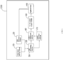
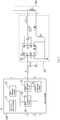
- FIG. 1 to FIG. 2 are a schematic block diagram and an application circuit diagram of the system for regulating the minimum output current of an LED dimming power supply provided by the present invention.
- the system 100 for regulating the minimum output current of an LED dimming power supply comprises an initial value setting module 10, a data detection module 20, a data processing module 30, an output adjustment module 40, a DC / DC current output module 50 electrically connected with the output adjustment module 40, a load 60 connected in series at the output of the DC / DC current output module 50, and an output regulation module 70.
- the LED dimming power supply is used to adjust the parameters of the connected load such as the brightness or the color temperature of the LED lamp. Therefore, the output current or output voltage of the LED dimming power supply can be controlled by a manual or automatic device.
- the system 100 for regulating the minimum output current of the LED dimming power supply may further comprises other functional modules such as a power module for providing a DC constant voltage to the DC / DC current output module 50, and a front-end power supply module providing the compliance power for the initial value setting module 10, the data detection module 20, the data processing module 30. All these above are well-known to those skilled in the art, and they will not be described in detail.
- the initial value setting module 10 is configured to preset a threshold value of a minimum output rated current of the LED dimming power supply and tune the control signal output by the output adjustment module 40 that controls the output value of the DC / DC current output module 50 to the minimum.
- the threshold value can be set according to the user's requirement or set by the provider of the LED dimming power supply in the factory. When the threshold value is set, the threshold value is the minimum output rated current of the LED dimming power supply. Meanwhile, the output current of the LED dimming power supply is a value between the minimum output rated current and the maximum output current.
- a plurality of LED lamps of the same type are usually powered by a plurality of power sources. If the minimum output rated current is not set, these same type of LED lamps are adjusted to the minimum brightness or other parameters such as color temperature, there will be some brighter, some darker, some higher color temperature, and some lower color temperature, and it will give people poor experience with light.
- the threshold value determines the minimum value for each parameter of each LED lamp of the same type when the LED lamp works. The setting of the threshold value can be set according to the selection of the specification parameters of various components of the LED dimming power supply.
- the threshold value can be written by a program set, while the principle is the same.
- the LED dimming power supply uses a microcontroller to reduce the size and the cost of the power supply. Therefore, the threshold value is programmed into the LED dimming power supply.
- the maximum output current of the LED dimming power supply the current is not adjusted by the output adjustment module 40.
- the output adjustment module 40 includes the PWM signal generator, the duty cycle of the PWM signal output by the PWM signal generator is 1, that is, the output adjustment module 40 does not adjust the output of the LED dimming power supply, At this moment, the output current of the LED dimming power supply is the maximum value.
- the control signal of the output adjustment module 40 should be the minimum value in the beginning.
- the output value of the DC / DC current output module 50 is the minimum.
- the initial value setting module 10 is further configured to tune the control signal output by the output adjustment module 40 that controls the output value of the DC / DC current output module 50 to the minimum.
- the data detection module 20 is used for detecting the load current flowing on the load 60.
- the magnitude of the load current flowing on the load is a technique well-known to those skilled in the art and will not be described in detail herein.
- the data detection module 20 can be designed and formed by electronic components.
- the data detection module 20 is integrated in the integrated circuit that is a microcontroller. One pin of the microcontroller is connected through a wire at one end of the load 60, a load current flowing through the load 60 can be detected.
- the data detection module 20 is electrically connected to the data processing module 30 to transmit the detected load current to the data processing module 30.
- the data processing module 30 is configured to compare the load current with a threshold value and output a comparison result.
- the data processing module 30 is also integrated into an integrated chip, that is, the microcontroller.
- the data processing module 30 can also be constructed by some electronic components, such as those known by those skilled in the art through transistors, regulator, and operational amplifiers.
- the data processing module 30 receives the threshold value of the initial value setting module 10 and the load current detected by the data detection module 20 and compares the threshold value with the load current so as to obtain a comparison value.
- the output adjustment module 40 is configured to adjust the output control signal according to the output result of the data processing module 30 when the load current is less than the threshold value to adjust the output voltage of the DC / DC current output module 50 to load the current value at the load 60 is equal to the threshold value.
- the output adjustment module 40 is also an executing module of the dimming command of the LED dimming power supply. That is, when the user needs to adjust the light-emitting parameters of the lamp connected to the LED dimming power supply, the output voltage of the LED dimming power supply is adjusted by the output adjustment module 40.
- the output voltage of the DC / DC current output module 50 is adjusted by adjusting the output of the output adjustment module 40 to adjust the output voltage of the LED dimming power supply.
- the output adjustment module 40 can be various electronic components that can adjust the output voltage, such as a dip switch, a PWM signal generator, and so on.
- the output adjustment module 40 is a PWM signal generator, which is also integrated in the integrated chip, that is, a microcontroller.
- the magnitude of the input voltage of the DC / DC current output module 50 can be adjusted by adjusting the duty cycle of the PWM signal output by the PWM signal generator, so as to adjust the magnitude of the current flowing on the load 60, to adjust the output of the LED dimming power supply.
- the load 60 can be replaced by various types of LED lamps in actual use.
- the output current of the DC / DC current output module 50 can be adjusted to the threshold value by adjusting the duty cycle of the PWM signal. Since the output of the output adjustment module 40 is initially the minimum value, the output of the DC / DC current output module 50 should also be the minimum value, so that if the load current detected by the data detection module 20 at this time is greater than the threshold value, it indicates that the LED dimming power supply has failed and is a failed power supply,
- the DC / DC current output module 50 may be a switching power supply chip that switch in high frequency through controllable switches (MOSFETs, etc.) utilizing the characteristics of energy storage of the capacitors or inductors and stores the input electrical energy in a capacitor (inductance), when the switch is off, the power is released to the load and provide energy.
- the ability to output power or voltage of the DC / DC current output module 50 is related to the duty cycle (the ratio of on-time of the switch to the entire period of the switch).
- the DC / DC current output module 50 can be used to Increase voltage and reduce voltage.
- the DC / DC current output module 50 is a buck conversion circuit, and the voltage value can be adjusted to an arbitrary value.
- the load 60 is connected in series at the output of the DC / DC current output module 50, so that the output voltage of the DC / DC current output module 50 is loaded on the load 60.
- the output regulation module 70 is configured to regulate the output value of the control signal of the output adjustment module 40 when the load current is equal to the threshold value by adjusting the control signal of the output adjustment module 40.
- the output regulation module 70 is also integrated into an integrated chip, that is, the microcontroller.
- the data regulation module 70 can also be constructed by some electronic components, such as those known by those skilled in the art through transistors, regulator, and operational amplifiers.
- the output signal value of the output adjustment module 40 When the regulated LED dimming power supply is turned on, the output signal value of the output adjustment module 40 will be greater than or equal to the output value regulated by the output regulation module 70, that is, the minimum value of the output current of the LED dimming power supply will be equal to the threshold value.
- the system 100 for regulating the minimum output current of the LED dimming power supply is capable of utilizing the initial value setting module 10, the data detection module 20, the data processing module 30 ,and the output regulation module 70 to make the load 60 modularization and standardization. It means that the resistance of the load 60 is designed to a standard value, and the load 60 is set in a standard module, when the batches of LED dimming power supply need to regulate the minimum output current.
- the output of the LED dimming power supply are electrically connected to the standard module provided with the load 60 to complete the setting of the minimum output current of the LED dimming power supply ,so as to avoid human error caused by manual calibration and be particularly suitable for the mass production calibration in the factory.
Landscapes
- Circuit Arrangement For Electric Light Sources In General (AREA)
Claims (8)
- Système (100) pour régler le courant de sortie minimal d'une alimentation électrique à gradation de diode électroluminescente, DEL, comprenant :un module de réglage de valeur initiale (10),un module de détection de données (20),un module de traitement de données (30),un module d'ajustement de sortie (40),un module de sortie de courant continu/continu, CC/CC, (50) relié électriquement au module d'ajustement de sortie, une charge étant reliée en série à la sortie du module de sortie de courant CC/CC, etun module de régulation de sortie (70),caractérisé par le fait quele module de réglage de valeur initiale est configuré pour prérégler une valeur de seuil d'un courant nominal de sortie minimal de l'alimentation électrique à gradation de DEL et accorder un signal de commande délivré par le module d'ajustement de sortie qui commande une valeur de sortie du module de sortie de courant CC/CC au minimum, le module de détection de données est configuré pour détecter un courant de charge circulant à travers la charge, le module de traitement de données est configuré pour comparer le courant de charge à la valeur de seuil et délivrer un résultat de comparaison, le module d'ajustement de sortie est configuré pour ajuster le signal de commande selon le résultat de comparaison du module de traitement de données, tandis que le courant de charge est inférieur à la valeur de seuil, afin d'ajuster la tension de sortie du module de sortie de courant CC/CC, et de s'assurer que la valeur de courant au niveau de la charge est égale à la valeur de seuil, le module de sortie de courant CC/CC est configuré pour convertir une tension constante CC d'entrée en un courant constant CC, et le module de régulation de sortie est configuré pour réguler la valeur de sortie du signal de commande du module d'ajustement de sortie lorsque le courant de charge est égal à la valeur de seuil en ajustant le signal de commande du module d'ajustement de sortie.
- Système pour régler le courant de sortie minimal d'une alimentation électrique à gradation de DEL selon la revendication 1, dans lequel la valeur de courant de sortie du module de sortie de courant CC/CC est supérieure ou égale à la valeur de seuil.
- Système pour régler le courant de sortie minimal d'une alimentation électrique à gradation de DEL selon la revendication 1 ou 2, dans lequel la charge est une résistance.
- Système pour régler le courant de sortie minimal d'une alimentation électrique à gradation de DEL selon l'une quelconque des revendications 1 à 3, dans lequel la résistance de la résistance est supérieure à 200 Ohms.
- Système pour régler le courant de sortie minimal d'une alimentation électrique à gradation de DEL selon l'une quelconque des revendications 1 à 4, dans lequel le module de réglage de valeur initiale, le module de détection de données et le module de traitement de données sont intégrés dans une microcontrôleur, et le microcontrôleur réalise leurs fonctions.
- Système pour régler le courant de sortie minimal d'une alimentation électrique à gradation de DEL selon l'une quelconque des revendications 1 à 5, dans lequel le signal de sortie du module d'ajustement de sortie est un signal de modulation d'impulsions en largeur, PWM.
- Système pour régler le courant de sortie minimal d'une alimentation électrique à gradation de DEL selon la revendication 6, dans lequel le module d'ajustement de sortie est intégré dans un microcontrôleur, et le microcontrôleur réalise sa fonction.
- Système pour régler le courant de sortie minimal d'une alimentation électrique à gradation de DEL selon l'une quelconque des revendications 1 à 7, dans lequel l'alimentation électrique à gradation de DEL comprend le module de réglage de valeur initiale, le module de détection de données, le module de traitement de données, le module d'ajustement de sortie et le module de sortie de courant CC/CC relié électriquement au module d'ajustement de sortie.
Applications Claiming Priority (1)
| Application Number | Priority Date | Filing Date | Title |
|---|---|---|---|
| CN201710256036.XA CN106954308B (zh) | 2017-04-19 | 2017-04-19 | 一种led调光电源最小输出电流的规制系统 |
Publications (2)
| Publication Number | Publication Date |
|---|---|
| EP3393209A1 EP3393209A1 (fr) | 2018-10-24 |
| EP3393209B1 true EP3393209B1 (fr) | 2020-01-08 |
Family
ID=59476218
Family Applications (1)
| Application Number | Title | Priority Date | Filing Date |
|---|---|---|---|
| EP18168017.4A Active EP3393209B1 (fr) | 2017-04-19 | 2018-04-18 | Système permettant de réguler le courant de sortie minimale d'une alimentation électrique de gradation de del |
Country Status (3)
| Country | Link |
|---|---|
| US (1) | US10172200B2 (fr) |
| EP (1) | EP3393209B1 (fr) |
| CN (1) | CN106954308B (fr) |
Families Citing this family (2)
| Publication number | Priority date | Publication date | Assignee | Title |
|---|---|---|---|---|
| CN108322959B (zh) * | 2017-11-03 | 2024-03-15 | 赛尔富电子有限公司 | 一种led灯具的调光系统 |
| CN113301685A (zh) * | 2021-06-11 | 2021-08-24 | 江苏亿奇仁照明科技有限公司 | 一种提高led灯具光效和寿命的节能系统及方法 |
Family Cites Families (15)
| Publication number | Priority date | Publication date | Assignee | Title |
|---|---|---|---|---|
| US8686668B2 (en) * | 2009-10-26 | 2014-04-01 | Koninklijke Philips N.V. | Current offset circuits for phase-cut power control |
| US8344659B2 (en) * | 2009-11-06 | 2013-01-01 | Neofocal Systems, Inc. | System and method for lighting power and control system |
| CN102264175A (zh) * | 2010-05-26 | 2011-11-30 | 马士科技有限公司 | 一种可分级调光的发光二极管灯调光装置 |
| CN102300355B (zh) * | 2010-06-25 | 2013-12-25 | 英飞特电子(杭州)股份有限公司 | 一种led调光系统 |
| CN202364422U (zh) * | 2011-09-19 | 2012-08-01 | 深圳市圣纳斯科技有限公司 | Led恒流调光电源系统 |
| CN105244928A (zh) * | 2014-07-09 | 2016-01-13 | 中兴通讯股份有限公司 | 大负载终端的电源控制方法及电源控制装置 |
| CN105338690B (zh) * | 2014-08-15 | 2018-07-17 | 赛尔富电子有限公司 | 一种led调光电源 |
| CN204046881U (zh) * | 2014-08-15 | 2014-12-24 | 宁波高新区赛尔富电子有限公司 | 一种led调光电源 |
| WO2016100928A1 (fr) * | 2014-12-19 | 2016-06-23 | Lutron Electronics Co., Inc. | Étalonnage d'un dispositif de commande de charge destiné à une source de lumière de diode électroluminescente |
| CN105188232B (zh) * | 2015-10-23 | 2017-10-24 | 深圳市奇脉电子技术有限公司 | Led恒流驱动电路、调光电路及其控制方法 |
| US9621031B1 (en) * | 2015-10-27 | 2017-04-11 | Stmicroelectronics International N.V. | Bus voltage correction circuit |
| CN106937432A (zh) * | 2015-12-31 | 2017-07-07 | 赛尔富电子有限公司 | 一种用于数字控制的调光电路 |
| CN205566720U (zh) * | 2016-03-03 | 2016-09-07 | 深圳迈睿智能科技有限公司 | 一种调光起始电压自适应的恒压调光电源 |
| CN107529240B (zh) * | 2016-06-22 | 2024-03-15 | 赛尔富电子有限公司 | 一种应用于led灯的电源电路 |
| CN206713120U (zh) * | 2017-04-19 | 2017-12-05 | 赛尔富电子有限公司 | 一种led调光电源最小输出电流的规制系统 |
-
2017
- 2017-04-19 CN CN201710256036.XA patent/CN106954308B/zh active Active
-
2018
- 2018-04-16 US US15/954,348 patent/US10172200B2/en active Active
- 2018-04-18 EP EP18168017.4A patent/EP3393209B1/fr active Active
Non-Patent Citations (1)
| Title |
|---|
| None * |
Also Published As
| Publication number | Publication date |
|---|---|
| EP3393209A1 (fr) | 2018-10-24 |
| US10172200B2 (en) | 2019-01-01 |
| US20180310372A1 (en) | 2018-10-25 |
| CN106954308B (zh) | 2023-12-22 |
| CN106954308A (zh) | 2017-07-14 |
Similar Documents
| Publication | Publication Date | Title |
|---|---|---|
| JP6339300B1 (ja) | 固体照明モジュール、照明回路、及び照明制御方法 | |
| EP2486772B1 (fr) | Circuit de commande de charge à boucle fermée doté d'une large gamme de sortie | |
| US9113521B2 (en) | Load control device for a light-emitting diode light source | |
| US11930574B2 (en) | Drive circuit for a light-emitting diode light source | |
| HK1243858A1 (zh) | 用於led照明系统的电流分路器 | |
| WO2020112838A1 (fr) | Dispositif de commande de charge conçu pour fonctionner dans des modes à deux fils et à trois fils | |
| US10172200B2 (en) | System for regulating the minimum output current of an LED dimming power supply | |
| KR102768450B1 (ko) | 가변 전력 용량 디밍 컨버터 | |
| US10701779B2 (en) | Drive device for illuminating device, illumination device, lighting system and method for controlling the lighting system | |
| CN206713120U (zh) | 一种led调光电源最小输出电流的规制系统 | |
| EP2911481B1 (fr) | Procédé et dispositif pour étalonner une commande de gradateur |
Legal Events
| Date | Code | Title | Description |
|---|---|---|---|
| PUAI | Public reference made under article 153(3) epc to a published international application that has entered the european phase |
Free format text: ORIGINAL CODE: 0009012 |
|
| STAA | Information on the status of an ep patent application or granted ep patent |
Free format text: STATUS: THE APPLICATION HAS BEEN PUBLISHED |
|
| AK | Designated contracting states |
Kind code of ref document: A1 Designated state(s): AL AT BE BG CH CY CZ DE DK EE ES FI FR GB GR HR HU IE IS IT LI LT LU LV MC MK MT NL NO PL PT RO RS SE SI SK SM TR |
|
| AX | Request for extension of the european patent |
Extension state: BA ME |
|
| STAA | Information on the status of an ep patent application or granted ep patent |
Free format text: STATUS: REQUEST FOR EXAMINATION WAS MADE |
|
| 17P | Request for examination filed |
Effective date: 20190410 |
|
| RBV | Designated contracting states (corrected) |
Designated state(s): AL AT BE BG CH CY CZ DE DK EE ES FI FR GB GR HR HU IE IS IT LI LT LU LV MC MK MT NL NO PL PT RO RS SE SI SK SM TR |
|
| GRAP | Despatch of communication of intention to grant a patent |
Free format text: ORIGINAL CODE: EPIDOSNIGR1 |
|
| STAA | Information on the status of an ep patent application or granted ep patent |
Free format text: STATUS: GRANT OF PATENT IS INTENDED |
|
| INTG | Intention to grant announced |
Effective date: 20190911 |
|
| RAP1 | Party data changed (applicant data changed or rights of an application transferred) |
Owner name: SELF ELECTRONICS CO., LTD. Owner name: LIN, WANJIONG Owner name: SELF ELECTRONICS GERMANY GMBH |
|
| RIN1 | Information on inventor provided before grant (corrected) |
Inventor name: ZHOU, XIAOYONG Inventor name: ZOU, XUEJUN Inventor name: YOU, XIAOBO |
|
| GRAS | Grant fee paid |
Free format text: ORIGINAL CODE: EPIDOSNIGR3 |
|
| GRAA | (expected) grant |
Free format text: ORIGINAL CODE: 0009210 |
|
| STAA | Information on the status of an ep patent application or granted ep patent |
Free format text: STATUS: THE PATENT HAS BEEN GRANTED |
|
| AK | Designated contracting states |
Kind code of ref document: B1 Designated state(s): AL AT BE BG CH CY CZ DE DK EE ES FI FR GB GR HR HU IE IS IT LI LT LU LV MC MK MT NL NO PL PT RO RS SE SI SK SM TR |
|
| REG | Reference to a national code |
Ref country code: GB Ref legal event code: FG4D |
|
| REG | Reference to a national code |
Ref country code: CH Ref legal event code: EP |
|
| REG | Reference to a national code |
Ref country code: IE Ref legal event code: FG4D |
|
| REG | Reference to a national code |
Ref country code: AT Ref legal event code: REF Ref document number: 1224331 Country of ref document: AT Kind code of ref document: T Effective date: 20200215 |
|
| REG | Reference to a national code |
Ref country code: DE Ref legal event code: R096 Ref document number: 602018001962 Country of ref document: DE |
|
| REG | Reference to a national code |
Ref country code: DE Ref legal event code: R079 Ref document number: 602018001962 Country of ref document: DE Free format text: PREVIOUS MAIN CLASS: H05B0033080000 Ipc: H05B0045000000 |
|
| REG | Reference to a national code |
Ref country code: NL Ref legal event code: MP Effective date: 20200108 |
|
| REG | Reference to a national code |
Ref country code: LT Ref legal event code: MG4D |
|
| PG25 | Lapsed in a contracting state [announced via postgrant information from national office to epo] |
Ref country code: LT Free format text: LAPSE BECAUSE OF FAILURE TO SUBMIT A TRANSLATION OF THE DESCRIPTION OR TO PAY THE FEE WITHIN THE PRESCRIBED TIME-LIMIT Effective date: 20200108 Ref country code: FI Free format text: LAPSE BECAUSE OF FAILURE TO SUBMIT A TRANSLATION OF THE DESCRIPTION OR TO PAY THE FEE WITHIN THE PRESCRIBED TIME-LIMIT Effective date: 20200108 Ref country code: NO Free format text: LAPSE BECAUSE OF FAILURE TO SUBMIT A TRANSLATION OF THE DESCRIPTION OR TO PAY THE FEE WITHIN THE PRESCRIBED TIME-LIMIT Effective date: 20200408 Ref country code: NL Free format text: LAPSE BECAUSE OF FAILURE TO SUBMIT A TRANSLATION OF THE DESCRIPTION OR TO PAY THE FEE WITHIN THE PRESCRIBED TIME-LIMIT Effective date: 20200108 Ref country code: RS Free format text: LAPSE BECAUSE OF FAILURE TO SUBMIT A TRANSLATION OF THE DESCRIPTION OR TO PAY THE FEE WITHIN THE PRESCRIBED TIME-LIMIT Effective date: 20200108 Ref country code: PT Free format text: LAPSE BECAUSE OF FAILURE TO SUBMIT A TRANSLATION OF THE DESCRIPTION OR TO PAY THE FEE WITHIN THE PRESCRIBED TIME-LIMIT Effective date: 20200531 |
|
| PG25 | Lapsed in a contracting state [announced via postgrant information from national office to epo] |
Ref country code: HR Free format text: LAPSE BECAUSE OF FAILURE TO SUBMIT A TRANSLATION OF THE DESCRIPTION OR TO PAY THE FEE WITHIN THE PRESCRIBED TIME-LIMIT Effective date: 20200108 Ref country code: LV Free format text: LAPSE BECAUSE OF FAILURE TO SUBMIT A TRANSLATION OF THE DESCRIPTION OR TO PAY THE FEE WITHIN THE PRESCRIBED TIME-LIMIT Effective date: 20200108 Ref country code: SE Free format text: LAPSE BECAUSE OF FAILURE TO SUBMIT A TRANSLATION OF THE DESCRIPTION OR TO PAY THE FEE WITHIN THE PRESCRIBED TIME-LIMIT Effective date: 20200108 Ref country code: GR Free format text: LAPSE BECAUSE OF FAILURE TO SUBMIT A TRANSLATION OF THE DESCRIPTION OR TO PAY THE FEE WITHIN THE PRESCRIBED TIME-LIMIT Effective date: 20200409 Ref country code: IS Free format text: LAPSE BECAUSE OF FAILURE TO SUBMIT A TRANSLATION OF THE DESCRIPTION OR TO PAY THE FEE WITHIN THE PRESCRIBED TIME-LIMIT Effective date: 20200508 Ref country code: BG Free format text: LAPSE BECAUSE OF FAILURE TO SUBMIT A TRANSLATION OF THE DESCRIPTION OR TO PAY THE FEE WITHIN THE PRESCRIBED TIME-LIMIT Effective date: 20200408 |
|
| REG | Reference to a national code |
Ref country code: DE Ref legal event code: R097 Ref document number: 602018001962 Country of ref document: DE |
|
| PG25 | Lapsed in a contracting state [announced via postgrant information from national office to epo] |
Ref country code: ES Free format text: LAPSE BECAUSE OF FAILURE TO SUBMIT A TRANSLATION OF THE DESCRIPTION OR TO PAY THE FEE WITHIN THE PRESCRIBED TIME-LIMIT Effective date: 20200108 Ref country code: RO Free format text: LAPSE BECAUSE OF FAILURE TO SUBMIT A TRANSLATION OF THE DESCRIPTION OR TO PAY THE FEE WITHIN THE PRESCRIBED TIME-LIMIT Effective date: 20200108 Ref country code: CZ Free format text: LAPSE BECAUSE OF FAILURE TO SUBMIT A TRANSLATION OF THE DESCRIPTION OR TO PAY THE FEE WITHIN THE PRESCRIBED TIME-LIMIT Effective date: 20200108 Ref country code: DK Free format text: LAPSE BECAUSE OF FAILURE TO SUBMIT A TRANSLATION OF THE DESCRIPTION OR TO PAY THE FEE WITHIN THE PRESCRIBED TIME-LIMIT Effective date: 20200108 Ref country code: EE Free format text: LAPSE BECAUSE OF FAILURE TO SUBMIT A TRANSLATION OF THE DESCRIPTION OR TO PAY THE FEE WITHIN THE PRESCRIBED TIME-LIMIT Effective date: 20200108 Ref country code: SM Free format text: LAPSE BECAUSE OF FAILURE TO SUBMIT A TRANSLATION OF THE DESCRIPTION OR TO PAY THE FEE WITHIN THE PRESCRIBED TIME-LIMIT Effective date: 20200108 Ref country code: SK Free format text: LAPSE BECAUSE OF FAILURE TO SUBMIT A TRANSLATION OF THE DESCRIPTION OR TO PAY THE FEE WITHIN THE PRESCRIBED TIME-LIMIT Effective date: 20200108 |
|
| PLBE | No opposition filed within time limit |
Free format text: ORIGINAL CODE: 0009261 |
|
| STAA | Information on the status of an ep patent application or granted ep patent |
Free format text: STATUS: NO OPPOSITION FILED WITHIN TIME LIMIT |
|
| REG | Reference to a national code |
Ref country code: AT Ref legal event code: MK05 Ref document number: 1224331 Country of ref document: AT Kind code of ref document: T Effective date: 20200108 |
|
| PG25 | Lapsed in a contracting state [announced via postgrant information from national office to epo] |
Ref country code: MC Free format text: LAPSE BECAUSE OF FAILURE TO SUBMIT A TRANSLATION OF THE DESCRIPTION OR TO PAY THE FEE WITHIN THE PRESCRIBED TIME-LIMIT Effective date: 20200108 |
|
| 26N | No opposition filed |
Effective date: 20201009 |
|
| PG25 | Lapsed in a contracting state [announced via postgrant information from national office to epo] |
Ref country code: FR Free format text: LAPSE BECAUSE OF NON-PAYMENT OF DUE FEES Effective date: 20200430 Ref country code: LU Free format text: LAPSE BECAUSE OF NON-PAYMENT OF DUE FEES Effective date: 20200418 Ref country code: AT Free format text: LAPSE BECAUSE OF FAILURE TO SUBMIT A TRANSLATION OF THE DESCRIPTION OR TO PAY THE FEE WITHIN THE PRESCRIBED TIME-LIMIT Effective date: 20200108 Ref country code: IT Free format text: LAPSE BECAUSE OF FAILURE TO SUBMIT A TRANSLATION OF THE DESCRIPTION OR TO PAY THE FEE WITHIN THE PRESCRIBED TIME-LIMIT Effective date: 20200108 |
|
| REG | Reference to a national code |
Ref country code: BE Ref legal event code: MM Effective date: 20200430 |
|
| PG25 | Lapsed in a contracting state [announced via postgrant information from national office to epo] |
Ref country code: BE Free format text: LAPSE BECAUSE OF NON-PAYMENT OF DUE FEES Effective date: 20200430 Ref country code: SI Free format text: LAPSE BECAUSE OF FAILURE TO SUBMIT A TRANSLATION OF THE DESCRIPTION OR TO PAY THE FEE WITHIN THE PRESCRIBED TIME-LIMIT Effective date: 20200108 Ref country code: PL Free format text: LAPSE BECAUSE OF FAILURE TO SUBMIT A TRANSLATION OF THE DESCRIPTION OR TO PAY THE FEE WITHIN THE PRESCRIBED TIME-LIMIT Effective date: 20200108 |
|
| PG25 | Lapsed in a contracting state [announced via postgrant information from national office to epo] |
Ref country code: IE Free format text: LAPSE BECAUSE OF NON-PAYMENT OF DUE FEES Effective date: 20200418 |
|
| PG25 | Lapsed in a contracting state [announced via postgrant information from national office to epo] |
Ref country code: LI Free format text: LAPSE BECAUSE OF NON-PAYMENT OF DUE FEES Effective date: 20210430 Ref country code: CH Free format text: LAPSE BECAUSE OF NON-PAYMENT OF DUE FEES Effective date: 20210430 |
|
| PG25 | Lapsed in a contracting state [announced via postgrant information from national office to epo] |
Ref country code: TR Free format text: LAPSE BECAUSE OF FAILURE TO SUBMIT A TRANSLATION OF THE DESCRIPTION OR TO PAY THE FEE WITHIN THE PRESCRIBED TIME-LIMIT Effective date: 20200108 Ref country code: MT Free format text: LAPSE BECAUSE OF FAILURE TO SUBMIT A TRANSLATION OF THE DESCRIPTION OR TO PAY THE FEE WITHIN THE PRESCRIBED TIME-LIMIT Effective date: 20200108 Ref country code: CY Free format text: LAPSE BECAUSE OF FAILURE TO SUBMIT A TRANSLATION OF THE DESCRIPTION OR TO PAY THE FEE WITHIN THE PRESCRIBED TIME-LIMIT Effective date: 20200108 |
|
| PG25 | Lapsed in a contracting state [announced via postgrant information from national office to epo] |
Ref country code: MK Free format text: LAPSE BECAUSE OF FAILURE TO SUBMIT A TRANSLATION OF THE DESCRIPTION OR TO PAY THE FEE WITHIN THE PRESCRIBED TIME-LIMIT Effective date: 20200108 Ref country code: AL Free format text: LAPSE BECAUSE OF FAILURE TO SUBMIT A TRANSLATION OF THE DESCRIPTION OR TO PAY THE FEE WITHIN THE PRESCRIBED TIME-LIMIT Effective date: 20200108 |
|
| GBPC | Gb: european patent ceased through non-payment of renewal fee |
Effective date: 20220418 |
|
| PG25 | Lapsed in a contracting state [announced via postgrant information from national office to epo] |
Ref country code: GB Free format text: LAPSE BECAUSE OF NON-PAYMENT OF DUE FEES Effective date: 20220418 |
|
| PGFP | Annual fee paid to national office [announced via postgrant information from national office to epo] |
Ref country code: DE Payment date: 20250430 Year of fee payment: 8 |