EP3398232B1 - Antenne configurable - Google Patents
Antenne configurable Download PDFInfo
- Publication number
- EP3398232B1 EP3398232B1 EP16822510.0A EP16822510A EP3398232B1 EP 3398232 B1 EP3398232 B1 EP 3398232B1 EP 16822510 A EP16822510 A EP 16822510A EP 3398232 B1 EP3398232 B1 EP 3398232B1
- Authority
- EP
- European Patent Office
- Prior art keywords
- antenna device
- antenna
- tracks
- electrical connection
- planes
- Prior art date
- Legal status (The legal status is an assumption and is not a legal conclusion. Google has not performed a legal analysis and makes no representation as to the accuracy of the status listed.)
- Active
Links
Images


Classifications
-
- H—ELECTRICITY
- H01—ELECTRIC ELEMENTS
- H01Q—ANTENNAS, i.e. RADIO AERIALS
- H01Q9/00—Electrically-short antennas having dimensions not more than twice the operating wavelength and consisting of conductive active radiating elements
- H01Q9/04—Resonant antennas
- H01Q9/0407—Substantially flat resonant element parallel to ground plane, e.g. patch antenna
- H01Q9/0421—Substantially flat resonant element parallel to ground plane, e.g. patch antenna with a shorting wall or a shorting pin at one end of the element
-
- H—ELECTRICITY
- H01—ELECTRIC ELEMENTS
- H01Q—ANTENNAS, i.e. RADIO AERIALS
- H01Q1/00—Details of, or arrangements associated with, antennas
- H01Q1/36—Structural form of radiating elements, e.g. cone, spiral, umbrella; Particular materials used therewith
-
- H—ELECTRICITY
- H01—ELECTRIC ELEMENTS
- H01Q—ANTENNAS, i.e. RADIO AERIALS
- H01Q7/00—Loop antennas with a substantially uniform current distribution around the loop and having a directional radiation pattern in a plane perpendicular to the plane of the loop
-
- H—ELECTRICITY
- H01—ELECTRIC ELEMENTS
- H01Q—ANTENNAS, i.e. RADIO AERIALS
- H01Q1/00—Details of, or arrangements associated with, antennas
- H01Q1/36—Structural form of radiating elements, e.g. cone, spiral, umbrella; Particular materials used therewith
- H01Q1/38—Structural form of radiating elements, e.g. cone, spiral, umbrella; Particular materials used therewith formed by a conductive layer on an insulating support
-
- H—ELECTRICITY
- H01—ELECTRIC ELEMENTS
- H01Q—ANTENNAS, i.e. RADIO AERIALS
- H01Q25/00—Antennas or antenna systems providing at least two radiating patterns
-
- H—ELECTRICITY
- H01—ELECTRIC ELEMENTS
- H01Q—ANTENNAS, i.e. RADIO AERIALS
- H01Q3/00—Arrangements for changing or varying the orientation or the shape of the directional pattern of the waves radiated from an antenna or antenna system
- H01Q3/01—Arrangements for changing or varying the orientation or the shape of the directional pattern of the waves radiated from an antenna or antenna system varying the shape of the antenna or antenna system
-
- H—ELECTRICITY
- H01—ELECTRIC ELEMENTS
- H01Q—ANTENNAS, i.e. RADIO AERIALS
- H01Q3/00—Arrangements for changing or varying the orientation or the shape of the directional pattern of the waves radiated from an antenna or antenna system
- H01Q3/24—Arrangements for changing or varying the orientation or the shape of the directional pattern of the waves radiated from an antenna or antenna system varying the orientation by switching energy from one active radiating element to another, e.g. for beam switching
-
- H—ELECTRICITY
- H01—ELECTRIC ELEMENTS
- H01Q—ANTENNAS, i.e. RADIO AERIALS
- H01Q5/00—Arrangements for simultaneous operation of antennas on two or more different wavebands, e.g. dual-band or multi-band arrangements
- H01Q5/30—Arrangements for providing operation on different wavebands
- H01Q5/307—Individual or coupled radiating elements, each element being fed in an unspecified way
- H01Q5/342—Individual or coupled radiating elements, each element being fed in an unspecified way for different propagation modes
- H01Q5/357—Individual or coupled radiating elements, each element being fed in an unspecified way for different propagation modes using a single feed point
- H01Q5/364—Creating multiple current paths
-
- H—ELECTRICITY
- H01—ELECTRIC ELEMENTS
- H01Q—ANTENNAS, i.e. RADIO AERIALS
- H01Q5/00—Arrangements for simultaneous operation of antennas on two or more different wavebands, e.g. dual-band or multi-band arrangements
- H01Q5/30—Arrangements for providing operation on different wavebands
- H01Q5/378—Combination of fed elements with parasitic elements
-
- H—ELECTRICITY
- H01—ELECTRIC ELEMENTS
- H01Q—ANTENNAS, i.e. RADIO AERIALS
- H01Q9/00—Electrically-short antennas having dimensions not more than twice the operating wavelength and consisting of conductive active radiating elements
- H01Q9/04—Resonant antennas
- H01Q9/0407—Substantially flat resonant element parallel to ground plane, e.g. patch antenna
- H01Q9/045—Substantially flat resonant element parallel to ground plane, e.g. patch antenna with particular feeding means
-
- H—ELECTRICITY
- H01—ELECTRIC ELEMENTS
- H01Q—ANTENNAS, i.e. RADIO AERIALS
- H01Q9/00—Electrically-short antennas having dimensions not more than twice the operating wavelength and consisting of conductive active radiating elements
- H01Q9/04—Resonant antennas
- H01Q9/30—Resonant antennas with feed to end of elongated active element, e.g. unipole
- H01Q9/42—Resonant antennas with feed to end of elongated active element, e.g. unipole with folded element, the folded parts being spaced apart a small fraction of the operating wavelength
Definitions
- This invention relates to an antenna device that is reconfigurable as various different types of antenna depending on how it is connected to a transmitter or receiver.
- Certain embodiments provide a single hardware solution configurable to multiple different hardware properties allowing the fixed hardware product to operate in any required band or frequency range or even as a multiband antenna. This may be achieved by user configurable pins. In some embodiments, it is possible dynamically to change the type of antenna structure.
- US 2012/0112968 A1 describes a module for an antenna system.
- the module includes a dielectric support and a branched electrically conductive pathway formed on or in the support.
- the pathway includes at least three arms having proximal and distal ends, the proximal ends being joined together.
- US 6204819 B1 describes multiple frequency band antennas having first and second conductive branches provided for use within wireless communication devices.
- US 2009/0251383 A1 describes a polarization switching antenna capable of switch a polarization without increase of an antenna installing space and also handling a variety of frequency bands.
- an antenna device According to a first aspect of the present invention, there is provided an antenna device according to claim 1.
- the first and/or the second tracks preferably have meandering configurations.
- the meandering configurations are carefully designed so that the first and/or the second tracks have predetermined inductances and optional internal capacitances.
- the meander allows the length of each track to be controlled, and also primarily serves to control the inductance of the respective track.
- portions of the first track in the first plane overlap portions of the second track in the second plane, with the overlapping portions allowing capacitive interactions between the first and second tracks.
- the at least first and second planes may be substantially parallel to each other, with a layer of dielectric material separating the at least first and second planes.
- Each of the at least first and second tracks may have first and second ends, with an electrical connection point at each of the respective first and second ends.
- One or other or both of the at least first and second tracks are disposed in both the first and the second planes, crossing from one plane to another by way of vias or other electrical connections between the planes.
- the electrical connection points are configured as pins extending from the laminate dielectric structure.
- the electrical connection points may be configured as surface mount pads, in which case it is preferable for all of the pads to be formed on one surface (for example an underside) of the laminate dielectric structure.
- the antenna device may be connected to external circuitry by way of a PCB provided with connections for the pins or surface mount pads corresponding to the surface mount pads on the antenna device.
- the laminate dielectric structure preferably has a cuboid shape or form factor.
- this surface is substantially square.
- four surface mount pads may be provided in respective corners or at mid-points of respective edges of a square surface.
- Additional connection schemas may be implemented by reconfiguring the corresponding connections on the PCB on which the antenna device is mounted. Dynamic reconfiguration of the antenna device may be effected by way of an RF switch which may, for example, be provided on the PCB. The RF switch may be operated so as to change the connection schema, for example by changing the ways in which the electrical connection points of the antenna device are connected to RF ground or to an RF feed.
- Certain embodiments make use of a multilayer configurable antenna structure within a laminate.
- the antenna structure may be such that it can be made to display a multitude of electrical properties with either a one-time setup or electronic dynamic control.
- the antenna structure can be configured or controlled to switch between radiating elements of varying types without host PCB modifications.
- the radiating element can take different forms.
- a single antenna device may be configured to operate in one or more of the following modes: dielectric antenna (including dielectric resonator antenna and/or dielectrically-loaded antenna), PIFA, PILA, loop, monopole, and/or capacitive-fed.
- the antenna device By providing one or more RF switches in combination with the antenna device, it is possible dynamically to reconfigure the electrical connections on the host PCB so as to allow a single antenna device to be dynamically switched between two or more of the following modes: dielectric antenna (including dielectric resonator antenna and/or dielectrically-loaded antenna), PIFA, PILA, loop, monopole, and/or capacitive-fed.
- the antenna device may be configured as an RF coupler.
- the RF properties of the structure include complex interactions involving Inductive coupling, capacitive coupling and coupling to its own internal structure. These properties are dependent on the setup and configuration used.
- Figures 1 and 2 show an exemplary embodiment of an antenna device 1 comprising first and second electrically conductive tracks 2, 3 disposed in first and second planes 4, 5 in a laminate dielectric structure.
- the first and second planes 4, 5 are separated by a layer of dielectric material 6. Additional layers 7, 8 of the same or different dielectric materials are provided on the top and bottom of the antenna device 1 so as to protect the electrically conductive tracks 2, 3.
- the ends of the first electrically conductive track 2 in the first plane 4 are provided with vias 9 to allow electrical connection to conductive surface mount pads P2 and P4.
- the ends of the second electrically conductive track 3 are provided with conductive surface mount pads P1 and P3.
- the surface mount pads P1 to P4 are exposed on the underside of the antenna device 1, and in the example shown, are disposed in the corners of a square underside.
- the first and second conductive tracks 2, 3 each have a meandering structure configured to provide predetermined inductances.
- the first and second conductive tracks 2, 3 have regions of mutual overlap 10, 11 as shown best in Figure 2 .
- the regions of mutual overlap 10, 11 give predetermined capacitive properties.
- Figures 3 and 4 show exploded views of the electrically conductive components of the antenna device 1, with the dielectric components omitted for clarity.
- the precise shape, configuration and path taken by each of the electrically conductive tracks 2, 3 depends on the particular antenna properties that are desired.
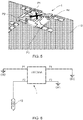
- Figure 5 shows the antenna device 1 mounted on a PCB 12 using surface mount technology.
- Surface mount pads P1, P3 and P4 are connected to ground by way of corresponding surface mount pads on the PCB 12.
- Surface mount pad P2 is connected to an RF feed by way of a corresponding surface mount pad on the PCB 12.
- Figure 6 shows a schematic representation of the arrangement of Figure 5 , with the RF feed indicated at 13.
- the antenna device 1 can operate in a dielectric resonator mode, with connection P2 being connected to the RF feed 13, and connections P1, P3 and P4 connected to RF ground.
- This configuration may be useful for dual band WiFi operation (e.g. at 2.4GHz and 5GHz).
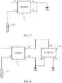
- Figure 7 shows a schematic outline of an alternative configuration, with connection P2 connected to the RF feed 13, connections P3 and P4 connected together and to RF ground, and connection P1 left unterminated (open circuit). It will be noted that P1 is connected internally to P3. In this configuration, the antenna device 1 operates as a PIFA.
- Figure 8 shows a schematic outline of an alternative configuration, with connection P2 connected to the RF feed 13, connection P1 left unterminated (open circuit), and connection P3 is connected to RF ground.
- Connection P4 is connected at RF1 to an RF switch 14, which is switchable so as to connect connection P4 either directly to RF ground via connection RF3, or to RF ground together with connection P3 via connection RF2.
- the antenna device 1 can be switched dynamically between PIFA mode and dielectric resonator mode by switching RF switch 14 between RF2 and RF3.
- the structure of the antenna device 1 is configured such that it exhibits both capacitive and inductive properties. Configuring the antenna device 1 so that it has both capacitive and inductive properties enables the antenna device 1 to change states depending on the arrangement of the pins or surface mount pads. A single antenna device 1 can therefore be used in situations where a capacitive arrangement is required or where an inductive arrangement is required.
- the internal structure of the antenna device defines the inductive and capacitive properties.
- the capacitance is defined internally between the top and bottom layer traces.
- the inductive properties are defined as a result of the length of each trace within the antenna.
- a benefit of this is that the manufacturing or electronic devices requiring antenna devices can be simplified by only requiring a single type of antenna device and costs can therefore be reduced.
- the structure is such that the electrical length between two paths are not the same to provide multiple inductive values, while the capacitive value fixed or removed completely by the pin arrangement.
- connections P2 and P4 could be connected to a balanced feed, with connections P1 and P3 unterminated, so as to realise a loop antenna.
- Other configurations can be implemented to realise a capacitive fed antenna or a PILA.
- One or more RF switches 14 can be provided to allow dynamic switching between the various antenna configurations.
- a particular advantage of certain embodiments of the present disclosure is that a single antenna device 1 can be used in several different ways, to cover different frequency bands, both passively and actively. This reduces the need to have many different types of antenna on hand when tailoring devices for different applications.
Landscapes
- Details Of Aerials (AREA)
Claims (13)
- Dispositif d'antenne (1) comprenant :
au moins des première et deuxième pistes électriquement conductrices (2, 3) disposées sur au moins des premier et deuxième plans (4, 5) dans une structure diélectrique stratifiée, chaque piste électriquement conductrice (2, 3) ayant au moins deux points de connexion électrique sur une surface externe de la structure diélectrique stratifiée, dans lequel chacune des première et deuxième pistes électriquement conductrices (2, 3) sont des pistes séparées à l'intérieur du dispositif d'antenne (1) ayant chacune des valeurs inductives différentes, et dans lequel les au moins première et deuxième pistes électriquement conductrices (2, 3) sont configurées de telle sorte que le dispositif d'antenne (1) présente à la fois des propriétés capacitives et inductives de sorte que, lors de l'utilisation, le dispositif d'antenne (1) soit reconfigurable entre une pluralité de types d'antennes différents en connectant les points de connexion électrique à un circuit externe dans différentes configurations, caractérisé en ce que l'une ou l'autre ou les deux des au moins première et deuxième pistes (2, 3) est ou sont disposée(s) à la fois sur les premier et deuxième plans (4, 5), en traversant d'un plan à l'autre par des vias (9) ou d'autres connexions électriques entre les plans. - Dispositif d'antenne (1) selon la revendication 1, dans lequel les première et / ou deuxième pistes (2, 3) ont des configurations sinueuses.
- Dispositif d'antenne (1) selon l'une quelconque des revendications précédentes, dans lequel des portions de la première piste (2) sur le premier plan (4) chevauchent des portions de la deuxième piste (3) sur le deuxième plan (5), avec les portions en chevauchement (10, 11) permettant des interactions capacitives entre les première et deuxième pistes (2, 3).
- Dispositif d'antenne (1) selon l'une quelconque des revendications précédentes, dans lequel les au moins premier et deuxième plans (4, 5) sont sensiblement parallèles l'un à l'autre, avec une couche de matériau diélectrique (6) séparant les au moins premier et deuxième plans (4, 5).
- Dispositif d'antenne (1) selon l'une quelconque des revendications précédentes, dans lequel chacune des au moins première et deuxième pistes (2, 3) a des première et deuxième extrémités, avec un point de connexion électrique au niveau de chacune des première et deuxième extrémités respectives.
- Dispositif d'antenne (1) selon l'une quelconque des revendications précédentes, dans lequel les points de connexion électrique sont configurés comme des broches s'étendant à partir de la structure diélectrique stratifiée.
- Dispositif d'antenne (1) selon l'une quelconque des revendications précédentes, dans lequel les points de connexion électrique sont configurés comme des plots de montage en surface (P1, P2, P3, P4).
- Dispositif d'antenne (1) selon la revendication 7, dans lequel tous les plots de montage en surface (P1, P2, P3, P4) sont formés sur une surface de la structure diélectrique stratifiée.
- Dispositif d'antenne (1) selon l'une quelconque des revendications 8, dans lequel la surface est une surface carrée.
- Dispositif d'antenne (1) selon la revendication 9, dans lequel quatre plots de montage en surface sont disposés sur la surface carrée, un dans chaque coin de la surface carrée ou un au milieu de chaque côté de la surface carrée.
- Dispositif d'antenne (1) selon l'une quelconque des revendications précédentes, dans lequel la structure diélectrique stratifiée a une forme cuboïde ou un facteur de forme.
- Dispositif d'antenne (1) selon l'une quelconque des revendications précédentes, configurable de manière sélective comme au moins deux parmi : une antenne diélectrique, une antenne plane en F inversé, PIFA, une antenne plane en L inversé, PILA, une antenne cadre, une antenne monopôle et une antenne à alimentation capacitive en changeant les connexions aux points de connexion électrique.
- Dispositif d'antenne (1) selon la revendication 12, en combinaison avec un commutateur RF configuré pour permettre une reconfiguration dynamique du dispositif d'antenne (1) en modifiant dynamiquement les connexions aux points de connexion électrique.
Applications Claiming Priority (2)
| Application Number | Priority Date | Filing Date | Title |
|---|---|---|---|
| GB1523090.7A GB2545918B (en) | 2015-12-30 | 2015-12-30 | Reconfigurable antenna |
| PCT/GB2016/054088 WO2017115089A1 (fr) | 2015-12-30 | 2016-12-30 | Antenne configurable |
Publications (2)
| Publication Number | Publication Date |
|---|---|
| EP3398232A1 EP3398232A1 (fr) | 2018-11-07 |
| EP3398232B1 true EP3398232B1 (fr) | 2020-08-19 |
Family
ID=55359199
Family Applications (1)
| Application Number | Title | Priority Date | Filing Date |
|---|---|---|---|
| EP16822510.0A Active EP3398232B1 (fr) | 2015-12-30 | 2016-12-30 | Antenne configurable |
Country Status (5)
| Country | Link |
|---|---|
| US (1) | US10897086B2 (fr) |
| EP (1) | EP3398232B1 (fr) |
| CA (1) | CA3010415C (fr) |
| GB (1) | GB2545918B (fr) |
| WO (1) | WO2017115089A1 (fr) |
Families Citing this family (3)
| Publication number | Priority date | Publication date | Assignee | Title |
|---|---|---|---|---|
| CN109149138B (zh) * | 2018-09-12 | 2020-12-18 | 东莞市合康电子有限公司 | 一种介质天线、介质天线装置及通信装置 |
| EP4463913A4 (fr) * | 2022-01-10 | 2025-03-19 | 2J Antennas USA, Corporation | Antenne à bande ultra-large et système associé |
| TWI825872B (zh) * | 2022-07-26 | 2023-12-11 | 宏碁股份有限公司 | 支援寬頻操作之行動裝置 |
Family Cites Families (24)
| Publication number | Priority date | Publication date | Assignee | Title |
|---|---|---|---|---|
| US6204819B1 (en) * | 2000-05-22 | 2001-03-20 | Telefonaktiebolaget L.M. Ericsson | Convertible loop/inverted-f antennas and wireless communicators incorporating the same |
| US6662028B1 (en) * | 2000-05-22 | 2003-12-09 | Telefonaktiebolaget L.M. Ericsson | Multiple frequency inverted-F antennas having multiple switchable feed points and wireless communicators incorporating the same |
| US6348897B1 (en) | 2001-02-16 | 2002-02-19 | Motorola, Inc. | Multi-function antenna system for radio communication device |
| EP1478045B1 (fr) * | 2003-05-16 | 2012-06-06 | Panasonic Corporation | Circuit à induction mutuelle |
| US7372411B2 (en) * | 2004-06-28 | 2008-05-13 | Nokia Corporation | Antenna arrangement and method for making the same |
| US7183976B2 (en) * | 2004-07-21 | 2007-02-27 | Mark Iv Industries Corp. | Compact inverted-F antenna |
| US7924226B2 (en) * | 2004-09-27 | 2011-04-12 | Fractus, S.A. | Tunable antenna |
| JP3889423B2 (ja) | 2004-12-16 | 2007-03-07 | 松下電器産業株式会社 | 偏波切り替えアンテナ装置 |
| US8866691B2 (en) * | 2007-04-20 | 2014-10-21 | Skycross, Inc. | Multimode antenna structure |
| US7724193B2 (en) * | 2007-07-24 | 2010-05-25 | Sony Ericsson Mobile Communications Ab | Printed circuit boards with a multi-plane antenna and methods for configuring the same |
| US9065177B2 (en) * | 2009-01-15 | 2015-06-23 | Broadcom Corporation | Three-dimensional antenna structure |
| JP2010239246A (ja) * | 2009-03-30 | 2010-10-21 | Fujitsu Ltd | モノポールとループを組み合わせた動作周波数を調整可能なアンテナ |
| GB2470205B (en) * | 2009-05-13 | 2013-05-22 | Antenova Ltd | Branched multiport antennas |
| CN102005640B (zh) * | 2009-08-28 | 2015-04-15 | 深圳富泰宏精密工业有限公司 | 无线通信装置 |
| CN102804502B (zh) | 2009-12-16 | 2015-12-02 | 阿丹特有限责任公司 | 超材料可重配置天线 |
| US8836594B2 (en) * | 2010-04-09 | 2014-09-16 | Board Of Trustees Of Michigan State University | Reconfigurable leaky wave antenna |
| KR101687632B1 (ko) * | 2010-05-10 | 2016-12-20 | 삼성전자주식회사 | 휴대용 단말기의 가변형 내장 안테나 장치 |
| EP2395602A1 (fr) * | 2010-06-08 | 2011-12-14 | Research In Motion Limited | Système de diversité d'antenne double basse fréquence |
| GB2500136B (en) * | 2010-10-15 | 2015-02-18 | Microsoft Corp | Parasitic folded loop antenna |
| CN102856631B (zh) * | 2011-06-28 | 2015-04-22 | 财团法人工业技术研究院 | 天线与其通信装置 |
| KR101659827B1 (ko) * | 2012-12-20 | 2016-09-26 | 가부시키가이샤 무라타 세이사쿠쇼 | 멀티밴드용 안테나 |
| CN204424454U (zh) * | 2013-02-06 | 2015-06-24 | 株式会社村田制作所 | 线圈装置和天线装置 |
| JP6508878B2 (ja) * | 2014-03-17 | 2019-05-08 | 株式会社トーキン | 軟磁性成型体 |
| JP6508207B2 (ja) * | 2014-07-10 | 2019-05-08 | 日本電気株式会社 | アンテナ、アンテナアレイ及び無線通信装置 |
-
2015
- 2015-12-30 GB GB1523090.7A patent/GB2545918B/en not_active Expired - Fee Related
-
2016
- 2016-12-30 CA CA3010415A patent/CA3010415C/fr active Active
- 2016-12-30 US US16/067,198 patent/US10897086B2/en active Active
- 2016-12-30 EP EP16822510.0A patent/EP3398232B1/fr active Active
- 2016-12-30 WO PCT/GB2016/054088 patent/WO2017115089A1/fr not_active Ceased
Non-Patent Citations (1)
| Title |
|---|
| None * |
Also Published As
| Publication number | Publication date |
|---|---|
| WO2017115089A1 (fr) | 2017-07-06 |
| US20190027829A1 (en) | 2019-01-24 |
| US10897086B2 (en) | 2021-01-19 |
| EP3398232A1 (fr) | 2018-11-07 |
| GB2545918B (en) | 2020-01-22 |
| CA3010415A1 (fr) | 2017-07-06 |
| GB2545918A (en) | 2017-07-05 |
| CA3010415C (fr) | 2024-02-20 |
| GB201523090D0 (en) | 2016-02-10 |
Similar Documents
| Publication | Publication Date | Title |
|---|---|---|
| KR102212366B1 (ko) | 근거리장 통신 및 비-근거리장 통신을 위한 공유 구조물들을 갖는 다수의 안테나들을 구비한 전자 디바이스 | |
| CN110176670B (zh) | 具有用于处理近场通信和非近场通信的隙缝的电子设备 | |
| US10535921B2 (en) | Reconfigurable multi-band antenna with four to ten ports | |
| EP3469656B1 (fr) | Système d'antenne destiné à un dispositif portable | |
| CN114258612B (zh) | 天线及电子设备 | |
| TWI555267B (zh) | 具有接收器分集的可調式天線系統 | |
| EP3350875B1 (fr) | Réglage d'isolation d'antennes multiples | |
| US20170256843A1 (en) | Reconfigurable casing antenna system | |
| US11387559B2 (en) | Coupled antenna system for multiband operation | |
| US10374289B2 (en) | Reconfigurable 4-port multi-band multi-function antenna with a grounded dipole antenna component | |
| CN111492535A (zh) | 一种用于无线通信设备的天线系统 | |
| WO2014172077A1 (fr) | Antenne multibande réglable intégrant des circuits passifs et actifs | |
| EP3214697B1 (fr) | Antenne et modul d'antenne la comprenant | |
| WO2018164255A1 (fr) | Dispositif de communication sans fil | |
| US9893427B2 (en) | Antenna-like matching component | |
| WO2014132590A1 (fr) | Antenne et dispositif électronique | |
| US10784562B2 (en) | Wireless communication chip having internal antenna, internal antenna for wireless communication chip, and method of fabricating wireless communication chip having internal antenna | |
| JP2012504361A (ja) | 多層アンテナ | |
| EP3398232B1 (fr) | Antenne configurable | |
| CN109273830A (zh) | 天线及移动设备 | |
| CN107078393A (zh) | 用于无线电子设备的双频带多层偶极子天线 | |
| CN100448102C (zh) | 天线装置 | |
| WO2013104656A1 (fr) | Structure d'antenne reconfigurable | |
| CN110556631B (zh) | 多频天线装置 |
Legal Events
| Date | Code | Title | Description |
|---|---|---|---|
| STAA | Information on the status of an ep patent application or granted ep patent |
Free format text: STATUS: UNKNOWN |
|
| STAA | Information on the status of an ep patent application or granted ep patent |
Free format text: STATUS: THE INTERNATIONAL PUBLICATION HAS BEEN MADE |
|
| PUAI | Public reference made under article 153(3) epc to a published international application that has entered the european phase |
Free format text: ORIGINAL CODE: 0009012 |
|
| STAA | Information on the status of an ep patent application or granted ep patent |
Free format text: STATUS: REQUEST FOR EXAMINATION WAS MADE |
|
| 17P | Request for examination filed |
Effective date: 20180702 |
|
| AK | Designated contracting states |
Kind code of ref document: A1 Designated state(s): AL AT BE BG CH CY CZ DE DK EE ES FI FR GB GR HR HU IE IS IT LI LT LU LV MC MK MT NL NO PL PT RO RS SE SI SK SM TR |
|
| AX | Request for extension of the european patent |
Extension state: BA ME |
|
| DAV | Request for validation of the european patent (deleted) | ||
| DAX | Request for extension of the european patent (deleted) | ||
| STAA | Information on the status of an ep patent application or granted ep patent |
Free format text: STATUS: EXAMINATION IS IN PROGRESS |
|
| 17Q | First examination report despatched |
Effective date: 20191024 |
|
| REG | Reference to a national code |
Ref country code: DE Ref legal event code: R079 Ref document number: 602016042447 Country of ref document: DE Free format text: PREVIOUS MAIN CLASS: H01Q0007000000 Ipc: H01Q0001380000 |
|
| GRAP | Despatch of communication of intention to grant a patent |
Free format text: ORIGINAL CODE: EPIDOSNIGR1 |
|
| STAA | Information on the status of an ep patent application or granted ep patent |
Free format text: STATUS: GRANT OF PATENT IS INTENDED |
|
| RIC1 | Information provided on ipc code assigned before grant |
Ipc: H01Q 9/42 20060101ALI20200310BHEP Ipc: H01Q 3/01 20060101ALI20200310BHEP Ipc: H01Q 5/378 20150101ALI20200310BHEP Ipc: H01Q 1/38 20060101AFI20200310BHEP Ipc: H01Q 5/364 20150101ALI20200310BHEP Ipc: H01Q 7/00 20060101ALI20200310BHEP |
|
| INTG | Intention to grant announced |
Effective date: 20200408 |
|
| GRAS | Grant fee paid |
Free format text: ORIGINAL CODE: EPIDOSNIGR3 |
|
| GRAA | (expected) grant |
Free format text: ORIGINAL CODE: 0009210 |
|
| STAA | Information on the status of an ep patent application or granted ep patent |
Free format text: STATUS: THE PATENT HAS BEEN GRANTED |
|
| AK | Designated contracting states |
Kind code of ref document: B1 Designated state(s): AL AT BE BG CH CY CZ DE DK EE ES FI FR GB GR HR HU IE IS IT LI LT LU LV MC MK MT NL NO PL PT RO RS SE SI SK SM TR |
|
| REG | Reference to a national code |
Ref country code: CH Ref legal event code: EP |
|
| REG | Reference to a national code |
Ref country code: DE Ref legal event code: R096 Ref document number: 602016042447 Country of ref document: DE |
|
| REG | Reference to a national code |
Ref country code: AT Ref legal event code: REF Ref document number: 1305003 Country of ref document: AT Kind code of ref document: T Effective date: 20200915 |
|
| REG | Reference to a national code |
Ref country code: IE Ref legal event code: FG4D |
|
| REG | Reference to a national code |
Ref country code: LT Ref legal event code: MG4D |
|
| REG | Reference to a national code |
Ref country code: NL Ref legal event code: MP Effective date: 20200819 |
|
| PG25 | Lapsed in a contracting state [announced via postgrant information from national office to epo] |
Ref country code: FI Free format text: LAPSE BECAUSE OF FAILURE TO SUBMIT A TRANSLATION OF THE DESCRIPTION OR TO PAY THE FEE WITHIN THE PRESCRIBED TIME-LIMIT Effective date: 20200819 Ref country code: SE Free format text: LAPSE BECAUSE OF FAILURE TO SUBMIT A TRANSLATION OF THE DESCRIPTION OR TO PAY THE FEE WITHIN THE PRESCRIBED TIME-LIMIT Effective date: 20200819 Ref country code: NO Free format text: LAPSE BECAUSE OF FAILURE TO SUBMIT A TRANSLATION OF THE DESCRIPTION OR TO PAY THE FEE WITHIN THE PRESCRIBED TIME-LIMIT Effective date: 20201119 Ref country code: GR Free format text: LAPSE BECAUSE OF FAILURE TO SUBMIT A TRANSLATION OF THE DESCRIPTION OR TO PAY THE FEE WITHIN THE PRESCRIBED TIME-LIMIT Effective date: 20201120 Ref country code: BG Free format text: LAPSE BECAUSE OF FAILURE TO SUBMIT A TRANSLATION OF THE DESCRIPTION OR TO PAY THE FEE WITHIN THE PRESCRIBED TIME-LIMIT Effective date: 20201119 Ref country code: PT Free format text: LAPSE BECAUSE OF FAILURE TO SUBMIT A TRANSLATION OF THE DESCRIPTION OR TO PAY THE FEE WITHIN THE PRESCRIBED TIME-LIMIT Effective date: 20201221 Ref country code: HR Free format text: LAPSE BECAUSE OF FAILURE TO SUBMIT A TRANSLATION OF THE DESCRIPTION OR TO PAY THE FEE WITHIN THE PRESCRIBED TIME-LIMIT Effective date: 20200819 Ref country code: LT Free format text: LAPSE BECAUSE OF FAILURE TO SUBMIT A TRANSLATION OF THE DESCRIPTION OR TO PAY THE FEE WITHIN THE PRESCRIBED TIME-LIMIT Effective date: 20200819 |
|
| REG | Reference to a national code |
Ref country code: AT Ref legal event code: MK05 Ref document number: 1305003 Country of ref document: AT Kind code of ref document: T Effective date: 20200819 |
|
| PG25 | Lapsed in a contracting state [announced via postgrant information from national office to epo] |
Ref country code: IS Free format text: LAPSE BECAUSE OF FAILURE TO SUBMIT A TRANSLATION OF THE DESCRIPTION OR TO PAY THE FEE WITHIN THE PRESCRIBED TIME-LIMIT Effective date: 20201219 Ref country code: PL Free format text: LAPSE BECAUSE OF FAILURE TO SUBMIT A TRANSLATION OF THE DESCRIPTION OR TO PAY THE FEE WITHIN THE PRESCRIBED TIME-LIMIT Effective date: 20200819 Ref country code: LV Free format text: LAPSE BECAUSE OF FAILURE TO SUBMIT A TRANSLATION OF THE DESCRIPTION OR TO PAY THE FEE WITHIN THE PRESCRIBED TIME-LIMIT Effective date: 20200819 Ref country code: RS Free format text: LAPSE BECAUSE OF FAILURE TO SUBMIT A TRANSLATION OF THE DESCRIPTION OR TO PAY THE FEE WITHIN THE PRESCRIBED TIME-LIMIT Effective date: 20200819 Ref country code: NL Free format text: LAPSE BECAUSE OF FAILURE TO SUBMIT A TRANSLATION OF THE DESCRIPTION OR TO PAY THE FEE WITHIN THE PRESCRIBED TIME-LIMIT Effective date: 20200819 |
|
| PG25 | Lapsed in a contracting state [announced via postgrant information from national office to epo] |
Ref country code: SM Free format text: LAPSE BECAUSE OF FAILURE TO SUBMIT A TRANSLATION OF THE DESCRIPTION OR TO PAY THE FEE WITHIN THE PRESCRIBED TIME-LIMIT Effective date: 20200819 Ref country code: EE Free format text: LAPSE BECAUSE OF FAILURE TO SUBMIT A TRANSLATION OF THE DESCRIPTION OR TO PAY THE FEE WITHIN THE PRESCRIBED TIME-LIMIT Effective date: 20200819 Ref country code: RO Free format text: LAPSE BECAUSE OF FAILURE TO SUBMIT A TRANSLATION OF THE DESCRIPTION OR TO PAY THE FEE WITHIN THE PRESCRIBED TIME-LIMIT Effective date: 20200819 Ref country code: DK Free format text: LAPSE BECAUSE OF FAILURE TO SUBMIT A TRANSLATION OF THE DESCRIPTION OR TO PAY THE FEE WITHIN THE PRESCRIBED TIME-LIMIT Effective date: 20200819 Ref country code: CZ Free format text: LAPSE BECAUSE OF FAILURE TO SUBMIT A TRANSLATION OF THE DESCRIPTION OR TO PAY THE FEE WITHIN THE PRESCRIBED TIME-LIMIT Effective date: 20200819 |
|
| REG | Reference to a national code |
Ref country code: DE Ref legal event code: R097 Ref document number: 602016042447 Country of ref document: DE |
|
| PG25 | Lapsed in a contracting state [announced via postgrant information from national office to epo] |
Ref country code: ES Free format text: LAPSE BECAUSE OF FAILURE TO SUBMIT A TRANSLATION OF THE DESCRIPTION OR TO PAY THE FEE WITHIN THE PRESCRIBED TIME-LIMIT Effective date: 20200819 Ref country code: AT Free format text: LAPSE BECAUSE OF FAILURE TO SUBMIT A TRANSLATION OF THE DESCRIPTION OR TO PAY THE FEE WITHIN THE PRESCRIBED TIME-LIMIT Effective date: 20200819 Ref country code: AL Free format text: LAPSE BECAUSE OF FAILURE TO SUBMIT A TRANSLATION OF THE DESCRIPTION OR TO PAY THE FEE WITHIN THE PRESCRIBED TIME-LIMIT Effective date: 20200819 |
|
| PLBE | No opposition filed within time limit |
Free format text: ORIGINAL CODE: 0009261 |
|
| STAA | Information on the status of an ep patent application or granted ep patent |
Free format text: STATUS: NO OPPOSITION FILED WITHIN TIME LIMIT |
|
| PG25 | Lapsed in a contracting state [announced via postgrant information from national office to epo] |
Ref country code: SK Free format text: LAPSE BECAUSE OF FAILURE TO SUBMIT A TRANSLATION OF THE DESCRIPTION OR TO PAY THE FEE WITHIN THE PRESCRIBED TIME-LIMIT Effective date: 20200819 |
|
| 26N | No opposition filed |
Effective date: 20210520 |
|
| PG25 | Lapsed in a contracting state [announced via postgrant information from national office to epo] |
Ref country code: IT Free format text: LAPSE BECAUSE OF FAILURE TO SUBMIT A TRANSLATION OF THE DESCRIPTION OR TO PAY THE FEE WITHIN THE PRESCRIBED TIME-LIMIT Effective date: 20200819 |
|
| REG | Reference to a national code |
Ref country code: CH Ref legal event code: PL |
|
| PG25 | Lapsed in a contracting state [announced via postgrant information from national office to epo] |
Ref country code: MC Free format text: LAPSE BECAUSE OF FAILURE TO SUBMIT A TRANSLATION OF THE DESCRIPTION OR TO PAY THE FEE WITHIN THE PRESCRIBED TIME-LIMIT Effective date: 20200819 Ref country code: SI Free format text: LAPSE BECAUSE OF FAILURE TO SUBMIT A TRANSLATION OF THE DESCRIPTION OR TO PAY THE FEE WITHIN THE PRESCRIBED TIME-LIMIT Effective date: 20200819 |
|
| REG | Reference to a national code |
Ref country code: BE Ref legal event code: MM Effective date: 20201231 |
|
| PG25 | Lapsed in a contracting state [announced via postgrant information from national office to epo] |
Ref country code: IE Free format text: LAPSE BECAUSE OF NON-PAYMENT OF DUE FEES Effective date: 20201230 Ref country code: LU Free format text: LAPSE BECAUSE OF NON-PAYMENT OF DUE FEES Effective date: 20201230 |
|
| PG25 | Lapsed in a contracting state [announced via postgrant information from national office to epo] |
Ref country code: CH Free format text: LAPSE BECAUSE OF NON-PAYMENT OF DUE FEES Effective date: 20201231 Ref country code: LI Free format text: LAPSE BECAUSE OF NON-PAYMENT OF DUE FEES Effective date: 20201231 |
|
| PG25 | Lapsed in a contracting state [announced via postgrant information from national office to epo] |
Ref country code: TR Free format text: LAPSE BECAUSE OF FAILURE TO SUBMIT A TRANSLATION OF THE DESCRIPTION OR TO PAY THE FEE WITHIN THE PRESCRIBED TIME-LIMIT Effective date: 20200819 Ref country code: MT Free format text: LAPSE BECAUSE OF FAILURE TO SUBMIT A TRANSLATION OF THE DESCRIPTION OR TO PAY THE FEE WITHIN THE PRESCRIBED TIME-LIMIT Effective date: 20200819 Ref country code: CY Free format text: LAPSE BECAUSE OF FAILURE TO SUBMIT A TRANSLATION OF THE DESCRIPTION OR TO PAY THE FEE WITHIN THE PRESCRIBED TIME-LIMIT Effective date: 20200819 |
|
| PG25 | Lapsed in a contracting state [announced via postgrant information from national office to epo] |
Ref country code: MK Free format text: LAPSE BECAUSE OF FAILURE TO SUBMIT A TRANSLATION OF THE DESCRIPTION OR TO PAY THE FEE WITHIN THE PRESCRIBED TIME-LIMIT Effective date: 20200819 |
|
| PG25 | Lapsed in a contracting state [announced via postgrant information from national office to epo] |
Ref country code: BE Free format text: LAPSE BECAUSE OF NON-PAYMENT OF DUE FEES Effective date: 20201231 |
|
| PGFP | Annual fee paid to national office [announced via postgrant information from national office to epo] |
Ref country code: GB Payment date: 20231212 Year of fee payment: 8 |
|
| PGFP | Annual fee paid to national office [announced via postgrant information from national office to epo] |
Ref country code: FR Payment date: 20231212 Year of fee payment: 8 Ref country code: DE Payment date: 20231214 Year of fee payment: 8 |
|
| REG | Reference to a national code |
Ref country code: DE Ref legal event code: R119 Ref document number: 602016042447 Country of ref document: DE |
|
| GBPC | Gb: european patent ceased through non-payment of renewal fee |
Effective date: 20241230 |
|
| PG25 | Lapsed in a contracting state [announced via postgrant information from national office to epo] |
Ref country code: DE Free format text: LAPSE BECAUSE OF NON-PAYMENT OF DUE FEES Effective date: 20250701 |
|
| PG25 | Lapsed in a contracting state [announced via postgrant information from national office to epo] |
Ref country code: GB Free format text: LAPSE BECAUSE OF NON-PAYMENT OF DUE FEES Effective date: 20241230 |
|
| PG25 | Lapsed in a contracting state [announced via postgrant information from national office to epo] |
Ref country code: FR Free format text: LAPSE BECAUSE OF NON-PAYMENT OF DUE FEES Effective date: 20241231 |