EP3399643A1 - Vorrichtung zur steuerung einer energieumwandlungsvorrichtung - Google Patents
Vorrichtung zur steuerung einer energieumwandlungsvorrichtung Download PDFInfo
- Publication number
- EP3399643A1 EP3399643A1 EP16881540.5A EP16881540A EP3399643A1 EP 3399643 A1 EP3399643 A1 EP 3399643A1 EP 16881540 A EP16881540 A EP 16881540A EP 3399643 A1 EP3399643 A1 EP 3399643A1
- Authority
- EP
- European Patent Office
- Prior art keywords
- voltage
- time period
- power
- conducting
- switch
- Prior art date
- Legal status (The legal status is an assumption and is not a legal conclusion. Google has not performed a legal analysis and makes no representation as to the accuracy of the status listed.)
- Ceased
Links
- 238000006243 chemical reaction Methods 0.000 title description 2
- 239000003990 capacitor Substances 0.000 claims abstract description 39
- 238000000034 method Methods 0.000 description 12
- 241001125929 Trisopterus luscus Species 0.000 description 11
- 101100150295 Mus musculus Scarf1 gene Proteins 0.000 description 9
- 101100433169 Rattus norvegicus Zdhhc2 gene Proteins 0.000 description 9
- 238000010586 diagram Methods 0.000 description 7
- 238000001514 detection method Methods 0.000 description 6
- 230000003313 weakening effect Effects 0.000 description 6
- 230000009467 reduction Effects 0.000 description 5
- 238000003860 storage Methods 0.000 description 5
- 230000007423 decrease Effects 0.000 description 4
- 230000006870 function Effects 0.000 description 4
- 230000004907 flux Effects 0.000 description 2
- 238000004804 winding Methods 0.000 description 2
- 101000582320 Homo sapiens Neurogenic differentiation factor 6 Proteins 0.000 description 1
- 102100030589 Neurogenic differentiation factor 6 Human genes 0.000 description 1
- 230000008859 change Effects 0.000 description 1
- 230000003247 decreasing effect Effects 0.000 description 1
- 238000009826 distribution Methods 0.000 description 1
- 230000000694 effects Effects 0.000 description 1
- 238000004519 manufacturing process Methods 0.000 description 1
- 238000012986 modification Methods 0.000 description 1
- 230000004048 modification Effects 0.000 description 1
Images


Classifications
-
- H—ELECTRICITY
- H02—GENERATION; CONVERSION OR DISTRIBUTION OF ELECTRIC POWER
- H02P—CONTROL OR REGULATION OF ELECTRIC MOTORS, ELECTRIC GENERATORS OR DYNAMO-ELECTRIC CONVERTERS; CONTROLLING TRANSFORMERS, REACTORS OR CHOKE COILS
- H02P27/00—Arrangements or methods for the control of AC motors characterised by the kind of supply voltage
- H02P27/04—Arrangements or methods for the control of AC motors characterised by the kind of supply voltage using variable-frequency supply voltage, e.g. inverter or converter supply voltage
- H02P27/06—Arrangements or methods for the control of AC motors characterised by the kind of supply voltage using variable-frequency supply voltage, e.g. inverter or converter supply voltage using DC to AC converters or inverters
-
- H—ELECTRICITY
- H02—GENERATION; CONVERSION OR DISTRIBUTION OF ELECTRIC POWER
- H02M—APPARATUS FOR CONVERSION BETWEEN AC AND AC, BETWEEN AC AND DC, OR BETWEEN DC AND DC, AND FOR USE WITH MAINS OR SIMILAR POWER SUPPLY SYSTEMS; CONVERSION OF DC OR AC INPUT POWER INTO SURGE OUTPUT POWER; CONTROL OR REGULATION THEREOF
- H02M3/00—Conversion of DC power input into DC power output
- H02M3/02—Conversion of DC power input into DC power output without intermediate conversion into AC
- H02M3/04—Conversion of DC power input into DC power output without intermediate conversion into AC by static converters
- H02M3/10—Conversion of DC power input into DC power output without intermediate conversion into AC by static converters using discharge tubes with control electrode or semiconductor devices with control electrode
- H02M3/145—Conversion of DC power input into DC power output without intermediate conversion into AC by static converters using discharge tubes with control electrode or semiconductor devices with control electrode using devices of a triode or transistor type requiring continuous application of a control signal
- H02M3/155—Conversion of DC power input into DC power output without intermediate conversion into AC by static converters using discharge tubes with control electrode or semiconductor devices with control electrode using devices of a triode or transistor type requiring continuous application of a control signal using semiconductor devices only
- H02M3/156—Conversion of DC power input into DC power output without intermediate conversion into AC by static converters using discharge tubes with control electrode or semiconductor devices with control electrode using devices of a triode or transistor type requiring continuous application of a control signal using semiconductor devices only with automatic control of output voltage or current, e.g. switching regulators
- H02M3/158—Conversion of DC power input into DC power output without intermediate conversion into AC by static converters using discharge tubes with control electrode or semiconductor devices with control electrode using devices of a triode or transistor type requiring continuous application of a control signal using semiconductor devices only with automatic control of output voltage or current, e.g. switching regulators including plural semiconductor devices as final control devices for a single load
- H02M3/1582—Buck-boost converters
-
- H—ELECTRICITY
- H02—GENERATION; CONVERSION OR DISTRIBUTION OF ELECTRIC POWER
- H02M—APPARATUS FOR CONVERSION BETWEEN AC AND AC, BETWEEN AC AND DC, OR BETWEEN DC AND DC, AND FOR USE WITH MAINS OR SIMILAR POWER SUPPLY SYSTEMS; CONVERSION OF DC OR AC INPUT POWER INTO SURGE OUTPUT POWER; CONTROL OR REGULATION THEREOF
- H02M5/00—Conversion of AC power input into AC power output, e.g. for change of voltage, for change of frequency, for change of number of phases
- H02M5/40—Conversion of AC power input into AC power output, e.g. for change of voltage, for change of frequency, for change of number of phases with intermediate conversion into DC
- H02M5/42—Conversion of AC power input into AC power output, e.g. for change of voltage, for change of frequency, for change of number of phases with intermediate conversion into DC by static converters
- H02M5/44—Conversion of AC power input into AC power output, e.g. for change of voltage, for change of frequency, for change of number of phases with intermediate conversion into DC by static converters using discharge tubes or semiconductor devices to convert the intermediate DC into AC
- H02M5/453—Conversion of AC power input into AC power output, e.g. for change of voltage, for change of frequency, for change of number of phases with intermediate conversion into DC by static converters using discharge tubes or semiconductor devices to convert the intermediate DC into AC using devices of a triode or transistor type requiring continuous application of a control signal
- H02M5/458—Conversion of AC power input into AC power output, e.g. for change of voltage, for change of frequency, for change of number of phases with intermediate conversion into DC by static converters using discharge tubes or semiconductor devices to convert the intermediate DC into AC using devices of a triode or transistor type requiring continuous application of a control signal using semiconductor devices only
-
- H—ELECTRICITY
- H02—GENERATION; CONVERSION OR DISTRIBUTION OF ELECTRIC POWER
- H02M—APPARATUS FOR CONVERSION BETWEEN AC AND AC, BETWEEN AC AND DC, OR BETWEEN DC AND DC, AND FOR USE WITH MAINS OR SIMILAR POWER SUPPLY SYSTEMS; CONVERSION OF DC OR AC INPUT POWER INTO SURGE OUTPUT POWER; CONTROL OR REGULATION THEREOF
- H02M5/00—Conversion of AC power input into AC power output, e.g. for change of voltage, for change of frequency, for change of number of phases
- H02M5/40—Conversion of AC power input into AC power output, e.g. for change of voltage, for change of frequency, for change of number of phases with intermediate conversion into DC
- H02M5/42—Conversion of AC power input into AC power output, e.g. for change of voltage, for change of frequency, for change of number of phases with intermediate conversion into DC by static converters
- H02M5/44—Conversion of AC power input into AC power output, e.g. for change of voltage, for change of frequency, for change of number of phases with intermediate conversion into DC by static converters using discharge tubes or semiconductor devices to convert the intermediate DC into AC
- H02M5/453—Conversion of AC power input into AC power output, e.g. for change of voltage, for change of frequency, for change of number of phases with intermediate conversion into DC by static converters using discharge tubes or semiconductor devices to convert the intermediate DC into AC using devices of a triode or transistor type requiring continuous application of a control signal
- H02M5/458—Conversion of AC power input into AC power output, e.g. for change of voltage, for change of frequency, for change of number of phases with intermediate conversion into DC by static converters using discharge tubes or semiconductor devices to convert the intermediate DC into AC using devices of a triode or transistor type requiring continuous application of a control signal using semiconductor devices only
- H02M5/4585—Conversion of AC power input into AC power output, e.g. for change of voltage, for change of frequency, for change of number of phases with intermediate conversion into DC by static converters using discharge tubes or semiconductor devices to convert the intermediate DC into AC using devices of a triode or transistor type requiring continuous application of a control signal using semiconductor devices only having a rectifier with controlled elements
-
- H—ELECTRICITY
- H02—GENERATION; CONVERSION OR DISTRIBUTION OF ELECTRIC POWER
- H02M—APPARATUS FOR CONVERSION BETWEEN AC AND AC, BETWEEN AC AND DC, OR BETWEEN DC AND DC, AND FOR USE WITH MAINS OR SIMILAR POWER SUPPLY SYSTEMS; CONVERSION OF DC OR AC INPUT POWER INTO SURGE OUTPUT POWER; CONTROL OR REGULATION THEREOF
- H02M7/00—Conversion of AC power input into DC power output; Conversion of DC power input into AC power output
- H02M7/02—Conversion of AC power input into DC power output without possibility of reversal
- H02M7/04—Conversion of AC power input into DC power output without possibility of reversal by static converters
- H02M7/06—Conversion of AC power input into DC power output without possibility of reversal by static converters using discharge tubes without control electrode or semiconductor devices without control electrode
-
- H—ELECTRICITY
- H02—GENERATION; CONVERSION OR DISTRIBUTION OF ELECTRIC POWER
- H02M—APPARATUS FOR CONVERSION BETWEEN AC AND AC, BETWEEN AC AND DC, OR BETWEEN DC AND DC, AND FOR USE WITH MAINS OR SIMILAR POWER SUPPLY SYSTEMS; CONVERSION OF DC OR AC INPUT POWER INTO SURGE OUTPUT POWER; CONTROL OR REGULATION THEREOF
- H02M7/00—Conversion of AC power input into DC power output; Conversion of DC power input into AC power output
- H02M7/42—Conversion of DC power input into AC power output without possibility of reversal
- H02M7/44—Conversion of DC power input into AC power output without possibility of reversal by static converters
- H02M7/48—Conversion of DC power input into AC power output without possibility of reversal by static converters using discharge tubes with control electrode or semiconductor devices with control electrode
-
- H—ELECTRICITY
- H02—GENERATION; CONVERSION OR DISTRIBUTION OF ELECTRIC POWER
- H02M—APPARATUS FOR CONVERSION BETWEEN AC AND AC, BETWEEN AC AND DC, OR BETWEEN DC AND DC, AND FOR USE WITH MAINS OR SIMILAR POWER SUPPLY SYSTEMS; CONVERSION OF DC OR AC INPUT POWER INTO SURGE OUTPUT POWER; CONTROL OR REGULATION THEREOF
- H02M7/00—Conversion of AC power input into DC power output; Conversion of DC power input into AC power output
- H02M7/66—Conversion of AC power input into DC power output; Conversion of DC power input into AC power output with possibility of reversal
- H02M7/68—Conversion of AC power input into DC power output; Conversion of DC power input into AC power output with possibility of reversal by static converters
- H02M7/72—Conversion of AC power input into DC power output; Conversion of DC power input into AC power output with possibility of reversal by static converters using discharge tubes with control electrode or semiconductor devices with control electrode
- H02M7/79—Conversion of AC power input into DC power output; Conversion of DC power input into AC power output with possibility of reversal by static converters using discharge tubes with control electrode or semiconductor devices with control electrode using devices of a triode or transistor type requiring continuous application of a control signal
- H02M7/797—Conversion of AC power input into DC power output; Conversion of DC power input into AC power output with possibility of reversal by static converters using discharge tubes with control electrode or semiconductor devices with control electrode using devices of a triode or transistor type requiring continuous application of a control signal using semiconductor devices only
-
- H—ELECTRICITY
- H02—GENERATION; CONVERSION OR DISTRIBUTION OF ELECTRIC POWER
- H02M—APPARATUS FOR CONVERSION BETWEEN AC AND AC, BETWEEN AC AND DC, OR BETWEEN DC AND DC, AND FOR USE WITH MAINS OR SIMILAR POWER SUPPLY SYSTEMS; CONVERSION OF DC OR AC INPUT POWER INTO SURGE OUTPUT POWER; CONTROL OR REGULATION THEREOF
- H02M1/00—Details of apparatus for conversion
- H02M1/0067—Converter structures employing plural converter units, other than for parallel operation of the units on a single load
- H02M1/007—Plural converter units in cascade
-
- H—ELECTRICITY
- H02—GENERATION; CONVERSION OR DISTRIBUTION OF ELECTRIC POWER
- H02P—CONTROL OR REGULATION OF ELECTRIC MOTORS, ELECTRIC GENERATORS OR DYNAMO-ELECTRIC CONVERTERS; CONTROLLING TRANSFORMERS, REACTORS OR CHOKE COILS
- H02P2201/00—Indexing scheme relating to controlling arrangements characterised by the converter used
- H02P2201/03—AC-DC converter stage controlled to provide a defined DC link voltage
-
- H—ELECTRICITY
- H02—GENERATION; CONVERSION OR DISTRIBUTION OF ELECTRIC POWER
- H02P—CONTROL OR REGULATION OF ELECTRIC MOTORS, ELECTRIC GENERATORS OR DYNAMO-ELECTRIC CONVERTERS; CONTROLLING TRANSFORMERS, REACTORS OR CHOKE COILS
- H02P2201/00—Indexing scheme relating to controlling arrangements characterised by the converter used
- H02P2201/07—DC-DC step-up or step-down converter inserted between the power supply and the inverter supplying the motor, e.g. to control voltage source fluctuations, to vary the motor speed
-
- H—ELECTRICITY
- H02—GENERATION; CONVERSION OR DISTRIBUTION OF ELECTRIC POWER
- H02P—CONTROL OR REGULATION OF ELECTRIC MOTORS, ELECTRIC GENERATORS OR DYNAMO-ELECTRIC CONVERTERS; CONTROLLING TRANSFORMERS, REACTORS OR CHOKE COILS
- H02P2201/00—Indexing scheme relating to controlling arrangements characterised by the converter used
- H02P2201/09—Boost converter, i.e. DC-DC step up converter increasing the voltage between the supply and the inverter driving the motor
Definitions
- the present invention relates to a power converter control device.
- Patent Documents 1 to 3 each disclose a direct power converter.
- This direct power converter includes a diode rectifier, an inverter, and a charge and discharge circuit.
- the diode rectifier full-wave rectifies a single-phase AC voltage, and outputs a rectified voltage after rectification across a pair of DC power supply lines (a DC link).
- the charge and discharge circuit is provided to the DC link, and includes a buffer circuit and a boost circuit.
- the buffer circuit has a switch and a capacitor connected in series to each other between the pair of DC power supply lines. When the switch is conducting, the capacitor discharges to provide power to the DC link.
- the boost circuit boosts the rectified voltage from the diode rectifier to charge the capacitor. This allows the charge and discharge circuit to receive power from the DC link.
- An input voltage (a DC voltage from the DC link) of the inverter matches the boosted voltage for the capacitor when the above-mentioned switch is conducting, and matches the rectified voltage when the switch is not conducting.
- the inverter receives the DC voltage from the DC link as an input, converts it into an AC voltage, and outputs the AC voltage.
- An object of the present application is thus to provide a direct power converter control device that enables driving of a motor with high efficiency.
- a first aspect of a power converter control device is a device for controlling, in a power converter including first and second DC power supply lines (LH, LL), a rectifying circuit (3), a discharge switch (Sc) and a capacitor (C4), a boost circuit (4a), and an inverter (5), the discharge switch, the rectifying circuit full-wave rectifying a single-phase AC voltage to a rectified voltage, and applying the rectified voltage across the first and second DC power supply lines, the discharge switch and the capacitor being connected in series to each other between the first and second DC power supply lines, the boost circuit boosting the rectified voltage to charge the capacitor, the inverter receiving, as an input, the rectified voltage as a DC voltage (Vdcl) across the first and second DC power supply lines when the discharge switch is not conducting, receiving, as an input, a voltage across the capacitor as the DC voltage when the discharge switch is conducting, converting the DC voltage as input into an AC voltage, and outputting the AC voltage to a motor (6), the power converter control device
- a second aspect of the power converter control device is the power converter control device according to the first aspect in which, when the rotational speed ( ⁇ m) is higher than the speed threshold ( ⁇ ref), the first time period (T1) has a length of zero.
- a third aspect of the power converter control device is the power converter control device according to the first or second aspect in which, when the rotational speed ( ⁇ m) is lower than the speed threshold ( ⁇ ref), the first time period (T1) is a time period in which the rectified voltage is greater than a predetermined value.
- a fourth aspect of the power converter control device is the power converter control device according to any one of the first to third aspects in which the charge and discharge time period setting unit (12) sets the speed threshold to the rotational speed when amplitude of the AC voltage applied to the motor (6) reaches an upper limit.
- the voltage across the capacitor is higher than the rectified voltage, and thus the DC voltage can be higher than the rectified voltage when the discharge switch is conducting.
- the DC voltage can be higher than the rectified voltage as the discharge switch is conducting in the second time period, but the DC voltage matches the rectified voltage as the discharge switch is maintained not conducting in the first time period. That is to say, the DC voltage higher than the rectified voltage cannot be input into the inverter in the first time period.
- the discharge switch is switched between conducting and not conducting in the second time period that is longer.
- the DC voltage when the rotational speed is high can thus be higher than the DC voltage when the rotational speed is low.
- the maximum value of a voltage (maximum output applied voltage) that can be applied to the motor can be increased with increasing second time period, and thus high-speed rotation and high-load operation of the motor can be achieved while suppressing an increase in current of the motor.
- the DC voltage can become small when the rotational speed is low.
- a time period in which the discharge switch is conducting i.e., a period in which the capacitor discharges
- Loss caused in the boost circuit is reduced as the amount of operation of the boost circuit decreases. Efficiency when the rotational speed is low can thus be improved.
- high-load operation can be achieved while suppressing the increase in current of the motor when the rotational speed is high, while efficiency is improved when the rotational speed is low.
- the maximum output applied voltage to the motor can be maximized.
- the DC voltage can be increased compared with a case where a time period in which the rectified voltage is smaller than a voltage reference value is used as the first time period.
- FIG. 1 is a block diagram showing the configuration of a direct power converter to which a control method shown in the present embodiment is applied.
- the direct power converter includes a converter 3, a power buffer circuit 4, and an inverter 5.
- the converter 3 is a single-phase rectifying circuit, and is connected to a single-phase AC power supply 1, for example, via a filter 2.
- the filter 2 includes a reactor L2 and a capacitor C2.
- the reactor L2 is connected between one of two output terminals of the single-phase AC power supply 1 and the converter 3.
- the capacitor C2 is connected in series to the reactor L2 between the two output terminals of the single-phase AC power supply 1.
- the filter 2 removes a high-frequency component of a current.
- the filter 2 may be omitted. Description will be made below while ignoring the function of the filter 2 for simplicity.
- the converter 3 uses, for example, a diode bridge, and includes diodes D31 to D34.
- the diodes D31 to D34 constitute a bridge circuit, single-phase full-wave rectify a single-phase AC voltage Vin, which is an input voltage input from the single-phase AC power supply 1, to convert it into a rectified voltage Vrec, and output the rectified voltage Vrec across DC power supply lines LH and LL (they form a so-called DC link).
- a potential higher than that applied to the DC power supply line LL is applied to the DC power supply line LH.
- An input current Iin flows from the single-phase AC power supply 1 into the converter 3.
- the power buffer circuit 4 is a circuit that provides and receives power to and from the DC link, and includes a boost circuit 4a, a buffer circuit 4b, and a diode D42.
- the buffer circuit 4b includes a capacitor C4.
- the boost circuit 4a boosts the rectified voltage Vrec to charge the capacitor C4.
- the buffer circuit 4b further includes a transistor (herein an insulated-gate bipolar transistor: hereinafter abbreviated as an "IGBT”) Sc connected in antiparallel to a diode D42.
- the transistor Sc is connected in series to the capacitor C4 between the DC power supply lines LH and LL at a side closer to the DC power supply line LH.
- connecting A and B in antiparallel refers to connecting A and B in parallel so that a forward direction of A and a forward direction of B are opposite to each other.
- a forward direction of the transistor Sc is a direction from the DC power supply line LL towards the DC power supply line LH
- a forward direction of the diode D42 is a direction from the DC power supply line LH towards the DC power supply line LL.
- the transistor Sc and the diode D42 can collectively be understood as a single switch element (first switch).
- the boost circuit 4a includes a diode D40, a reactor L4, and a transistor (herein an IGBT) SL, for example.
- the diode D40 includes a cathode and an anode, and the cathode is connected between the first switch and the capacitor C4.
- the reactor L4 is connected between the DC power supply line LH and the anode of the diode D40.
- the transistor SL is connected between the DC power supply line LL and the anode of the diode D40.
- a diode D41 is connected in antiparallel to the transistor SL, and they can collectively be understood as a single switch element (second switch).
- the boost circuit 4a is known as a so-called boost chopper.
- the capacitor C4 is charged by the boost circuit 4a, and a voltage Vc higher than the rectified voltage Vrec is generated across the capacitor C4. Specifically, a current is allowed to flow from the DC power supply line LH to the DC power supply line LL via the second switch to store energy in the reactor L4, and then the second switch is turned off to store the energy in the capacitor C4 via the diode D40. This enables the power buffer circuit 4 to receive power from the DC link.
- a current basically does not flow through the diode D42.
- the first switch is conducting or not thus depends solely on whether the transistor Sc is conducting or not. Not only the transistor Sc but also the first switch (a discharge switch) including the transistor Sc and the diode D42 is thus hereinafter also referred to as a switch Sc.
- the switch Sc When the switch Sc is conducting, the capacitor C4 discharges so that the power buffer circuit 4 can provide power to the DC link.
- a current basically does not flow through the diode D41.
- the second switch is conducting or not thus depends solely on whether the transistor SL is conducting or not. Not only the transistor SL but also the second switch including the transistor SL and the diode D41 is thus hereinafter also referred to as a switch SL.
- the diode D42 is connected on the DC power supply line LH between the reactor L4 and the switch Sc.
- a forward direction of the diode D42 is a direction from the converter 3 towards the inverter 5.
- the diode D42 prevents a short circuit of the reactor L4 when the switch Sc is turned on, for example.
- the inverter 5 converts the DC voltage across the DC power supply lines LH and LL into an AC voltage, and outputs the AC voltage to output terminals Pu, Pv, and Pw. When this is described in terms of power, the inverter 5 receives DC power from the DC link as an input, and outputs AC power to a motor 6.
- the inverter 5 includes six switching elements Sup, Svp, Swp, Sun, Svn, and Swn.
- the switching elements Sup, Svp, and Swp are respectively connected between the output terminals Pu, Pv, and Pw and the DC power supply line LH, and the switching elements Sun, Svn, and Swn are respectively connected between the output terminals Pu, Pv, and Pw and the DC power supply line LL.
- the inverter 5 forms a so-called voltage source inverter, and includes six diodes Dup, Dvp, Dwp, Dun, Dvn, and Dwn.
- the diodes Dup, Dvp, Dwp, Dun, Dvn, and Dwn are arranged with their cathodes being directed towards the DC power supply line LH and their anodes being directed towards the DC power supply line LL.
- the diode Dup is connected in parallel to the switching element Sup between the output terminal Pu and the DC power supply line LH.
- the diodes Dvp, Dwp, Dun, Dvn, and Dwn are respectively connected in parallel to the switching elements Svp, Swp, Sun, Svn, and Swn.
- IGBTs are used as the switching elements Sup, Svp, Swp, Sun, Svn, and Swn, for example.
- FIG. 1 shows an equivalent circuit of the motor 6.
- an inductance component Lu and a resistance component Ru of a winding of a U phase are connected in series, and one end of the series-connected body is connected to the output terminal Pu. The same applies to windings of a V phase and a W phase. The other ends of these series-connected bodies are connected together.
- a control device 10 outputs switch signals to the switches SL and Sc and the inverter 5 to control the power converter. A method of controlling the power converter will be described below.
- the rectified voltage Vrec can be input into the inverter 5 when the switch Sc is not conducting.
- the voltage Vc across the capacitor C4 can be input into the inverter 5 when the switch Sc is conducting. That is to say, a DC voltage Vdcl input into the inverter 5 matches the rectified voltage Vrec when the switch Sc is not conducting, and matches the voltage Vc when the switch Sc is conducting.
- a time period T1 in which the switch Sc is maintained not conducting and a time period T2 in which the switch Sc is switched between conducting and not conducting are introduced.
- the time period T2 is a time period other than the time period T1.
- the time period T1 thus decreases with increasing time period T1.
- FIG. 2 schematically shows examples of the DC voltage Vdcl input into the inverter 5 and a switch state of the switch Sc.
- the single-phase AC voltage Vin, the input current Iin, and a current iL flowing through the reactor L4 are also shown for reference.
- the switch Sc is maintained not conducting (off in FIG. 2 ) in the time period T1.
- the switch state is blackened in the time period T2.
- the switch Sc is repeatedly switched between conducting and not conducting in the time period T2.
- the DC voltage Vdcl matches the voltage Vc when the switch Sc is conducting, and matches the rectified voltage Vrec when the switch Sc is not conducting.
- an average of the DC voltage Vdcl can be controlled to be between the rectified voltage Vrec and the voltage Vc in accordance with a duty at which the switch Sc is conducting. This means that, in the time period T2, the average of the DC voltage Vdcl can be increased above the rectified voltage Vrec.
- the average of the DC voltage Vdcl herein refers to an average (hereinafter, also referred to as a first average) of the DC voltage Vdcl in switching periods of the switch Sc, for example.
- the DC voltage Vdcl matches the rectified voltage Vrec in the time period T1, and the average of the DC voltage Vdcl can be controlled to be a desired value higher than the rectified voltage Vrec in the time period T2.
- the relationship between the maximum value of an average (hereinafter, referred to as a second average) of the DC voltage Vdcl in a single period of the single-phase AC voltage Vin and the length of the time period T1 will be considered next.
- the DC voltage Vdc1 matches the rectified voltage Vrec in the time period T1, and the DC voltage Vdc1 can be controlled to be the value higher than the rectified voltage Vrec in the time period T2.
- the maximum value of the second average of the DC voltage Vdc1 can thus be increased with decreasing time period T1.
- the maximum value of the second average of the DC voltage Vdcl decreases with increasing time period T1.
- the time period T1 is set to be shorter when a rotational speed com of the motor 6 is higher than a speed threshold than when the rotational speed com is lower than the speed threshold.
- the time period T1 is set to be zero, for example.
- the DC voltage Vdcl can be controlled to be maximized from a viewpoint of the length of the time period T1.
- the time period T1 is set to be long when the rotational speed com is low.
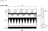
- FIG. 3 schematically shows examples of the DC voltage Vdcl and the switch state of the switch Sc when zero is used as the time period T1. Also in the example of FIG. 3 , the single-phase AC voltage Vin, the input current Iin, and the current iL are shown for reference. As illustrated in FIG. 3 , the switch Sc is repeatedly switched between conducting and not conducting in the entire time period (time period T2). The first average of the DC voltage Vdcl can thus be higher than the rectified voltage Vrec in the entire time period.
- the amplitude of the AC voltage applied to the motor 6 increases with increasing rotational speed ⁇ m of the motor 6.
- the maximum value of the amplitude of the AC voltage that the inverter 5 can output to the motor 6 depends on the DC voltage Vdcl. Specifically, the maximum value increases with increasing DC voltage Vdcl. Thus, the DC voltage Vdcl is not required to be increased when the rotational speed ⁇ m is low.
- the time period T1 is thus set to be long when the rotational speed ⁇ m is low (e.g., FIG. 2 ). This can reduce the maximum value of the second average of the DC voltage Vdcl when the rotational speed ⁇ m is low. If it is assumed that the duty in the time period T2 is not changed by the change of the length of the time period T1 for simplicity, for example, the second average of the DC voltage Vdcl is reduced by extension of the time period T1.
- a time period in which the switch Sc can be conducting that is, a time period in which the capacitor C4 can discharge decreases, and the amount of discharge can be reduced.
- the amount of charge and the amount of discharge of the capacitor C4 are controlled to be balanced, and thus the amount of charge of the capacitor C4 by the boost circuit 4a is reduced by reduction in amount of discharge. That is to say, a time period in which the switch SL is on is shorter when the rotational speed ⁇ m is lower than the speed threshold than when the rotational speed ⁇ m is higher than the speed threshold. This reduces a current flowing through the boost circuit 4a. Loss caused in the boost circuit 4a is thus also reduced.
- the time period T1 is set to be long to reduce the DC voltage Vdcl, the motor 6 can be driven with higher efficiency compared with a case where the time period T1 is set to be short.
- the time period T1 is set to be short when the rotational speed ⁇ m is high (e.g., FIG. 3 ).
- This can increase the maximum value of the second average of the DC voltage Vdcl when the rotational speed ⁇ m is high. That is to say, the DC voltage Vdcl can be controlled to be higher compared with a case where the time period T1 is set to be long. An AC voltage having larger amplitude can thus be output to the motor 6. This enables the motor 6 to be driven properly at a high rotational speed ⁇ m.
- the rotational speed ⁇ m can be increased, for example, by performing field weakening control (or flux weakening control, the same applies to the following).
- field weakening control or flux weakening control, the same applies to the following.
- the amplitude of the AC current flowing through the motor 6 increases rapidly with increasing rotational speed ⁇ m.
- the increase in current is undesirable, for example, because the current capacity of the circuit (the converter 3, the power buffer circuit 4, the inverter 5, and the motor 6) is required to be raised.
- the DC voltage Vdcl when the rotational speed ⁇ m is higher than the speed threshold, the DC voltage Vdcl can be controlled to be higher, and the inverter 5 can output the AC voltage having larger amplitude to the motor 6.
- a value of the rotational speed ⁇ m that requires the field weakening control can be increased. This can reduce the amplitude of the AC current flowing through the motor 6.
- the current capacity that the circuit is required to have can be reduced, leading to reduction in manufacturing cost.
- a speed detection unit 9 and the control device 10 are provided.
- the speed detection unit 9 detects the rotational speed ⁇ m of the motor 6.
- AC currents iu, iv, and iw flowing through the motor 6 are input into the speed detection unit 9.
- the AC currents iu, iv, and iw are detected by a known current detection unit.
- the speed detection unit 9 calculates the rotational speed ⁇ m of the motor 6 on the basis of the AC currents iu, iv, and iw, and outputs it to the control device 10.
- the control device 10 includes a switch control unit 11 and a charge and discharge time period setting unit 12.
- the control device 10 herein includes a microcomputer and a storage device.
- the microcomputer performs processing steps (i.e., procedures) written in a program.
- the above-mentioned storage device can be formed by one or more various storage devices, such as read only memory (ROM), random access memory (RAM), rewritable non-volatile memory (e.g., erasable programmable ROM (EPROM)), and a hard disk drive.
- ROM read only memory
- RAM random access memory
- EPROM erasable programmable ROM
- the storage device stores various pieces of information, data, and the like, stores the program executed by the microcomputer, and provides a work area for executing the program.
- the microcomputer can be understood to function as various units corresponding to the respective processing steps written in the program, or to achieve various functions corresponding to the respective processing steps.
- the control device 10 is not limited to this, and some or all of various procedures performed by the control device 10 or various units or various functions achieved by the control device 10 may be achieved by hardware.
- the rotational speed ⁇ m detected by the speed detection unit 9 is input into the charge and discharge time period setting unit 12.
- the charge and discharge time period setting unit 12 sets the length of the time period T1 (and, further, the time period T2) on the basis of the rotational speed ⁇ m as described above, and outputs information M showing the length of the time period T1 to the switch control unit 11.
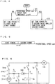
- FIG. 4 is a flowchart showing an example of operation of the charge and discharge time period setting unit 12, and FIG. 5 is a diagram for explaining the operation.
- the charge and discharge time period setting unit 12 first determines whether the rotational speed ⁇ m is higher than a speed threshold ⁇ ref in step ST1.
- the speed threshold ⁇ ref is stored in a storage, for example, and the charge and discharge time period setting unit 12 reads it, and determines whether the rotational speed ⁇ m is higher than the speed threshold ⁇ ref.
- the determination can be made, for example, using a comparator.
- the charge and discharge time period setting unit 12 determines the time period T1 as a first value in step ST2. Control based on the first value for the time period T1 is hereinafter also referred to as a first scheme.
- the charge and discharge time period setting unit 12 sets the time period T1 to a second value (e.g., zero) that is smaller than the first value in step ST2.
- Control based on the second value for the time period T1 is hereinafter also referred to as a second scheme.
- the first scheme is used when the rotational speed ⁇ m is lower than the speed threshold ⁇ ref
- the second scheme is used when the rotational speed ⁇ m is higher than the speed threshold ⁇ ref as shown in FIG. 5 .
- the switch control unit 11 generates control signals SSc, SSL, SSup, SSvp, SSwp, SSun, SSvn, SSvn, and SSwn for the switches SL and Sc of the power buffer circuit 4 and the switching elements Sup, Sun, Svp, Svn, Swp, and Swn of the inverter 5, and outputs them to the power buffer circuit 4 and the inverter 5.
- the rectified voltage Vrec when a time period in which the rectified voltage Vrec is smaller than the voltage reference value Vref is used as the time period T1, the rectified voltage Vrec near a bottom value (zero) appears as the DC voltage Vdc1 in the time period T1. That is to say, the DC voltage Vdcl can be increased by using the time period in which the rectified voltage Vrec is greater than the voltage reference value Vref as the time period T1. This is desirable because the AC voltage from the single-phase AC power supply 1 is used effectively.
- a plurality of speed thresholds may be provided.
- the time period T1 may be set to the first value when the rotational speed ⁇ m is lower than a first speed threshold, may be set to the second value ( ⁇ the first value) when the rotational speed ⁇ m is higher than the first speed threshold and is lower than a second speed threshold, and may be set to a third value ( ⁇ the second value) when the rotational speed ⁇ m is higher than the second speed threshold.
- the time periods T1 and T2 are switched each one-quarter period of the single-phase AC voltage Vin.
- the time period T1 is set to zero in the second scheme used when the rotational speed ⁇ m is higher than the speed threshold ⁇ ref (see FIG. 4 ).
- the second term of the rightmost side of the equation (1) indicates power ripple.
- a variation range of the input power Pin is the amplitude of the second term of the rightmost side of the equation (1), and is indicated by Vm ⁇ Im/2.
- Power that the converter 3 outputs to the DC link is ideally equal to the input power Pin input into the converter 3.
- the input power Pin can thus be understood as power input into the DC link.
- the power buffer circuit 4 should provide and receive power to and from the DC link so that the amplitude of the second term of the rightmost side of the equation (1) is reduced.
- the power provided and received by the power buffer circuit 4 is hereinafter referred to as buffer power Pbuf.
- the buffer power Pbuf is expressed by the product of a DC part (Vm ⁇ Im/2) of the input power Pin input from the single-phase AC power supply 1 (or further via the filter 2: the same applies to the following), a cosine value cos(2 ⁇ t) of a value (2 ⁇ t) that is twice the phase angle ⁇ t, and the variable k.
- FIG. 6 shows graphs each showing examples of the power. Two graphs are shown in the example of FIG. 6 , and each of the graphs shows the input power Pin, the buffer power Pbuf, and output power Pout. The output power Pout is power output from the inverter 5, and will be described below. These graphs differ in variable k.
- the buffer power Pbuf takes a positive value in a second time period T12 in which the phase angle ⁇ t of the single-phase AC voltage is 0 to ⁇ /4 inclusive, 3 ⁇ /4 to 5 ⁇ /4 inclusive, or 7 ⁇ /4 to 2 ⁇ inclusive, and takes a negative value in a first time period T11 other than the second time period T12. That is to say, the power buffer circuit 4 outputs the absolute value of the buffer power Pbuf to the DC link in the second time period T12, and receives the absolute value of the buffer power Pbuf from the DC link in the first time period T11.
- the single-phase AC voltage Vin is expressed by Vm ⁇ sin( ⁇ t), and thus, by describing the above-mentioned range in another way, it can also be said that the power buffer circuit 4 outputs positive power when the absolute value of the single-phase AC voltage Vin is smaller than a value that is 1/ ⁇ 2 times the crest value Vm thereof, and outputs negative power when the absolute value of the single-phase AC voltage Vin is greater than the value that is 1/ ⁇ 2 times the crest value Vm thereof.
- the output power Pout output from the inverter 5 is expressed by an equation shown below using the input power Pin and the buffer power Pbuf.
- the DC power Pdc input into the inverter 5 and the output power Pout output from the inverter 5 are ideally equal to each other.
- a variation range of ripple of the output power Pout is indicated by (1 - k) ⁇ Vm ⁇ Im/2. Since the variable k is greater than 0 and equal to or smaller than 1, the variation range is smaller than a variation range of the ripple power Pin (amplitude of the second term of the rightmost side of the equation (1)). That is to say, the power buffer circuit 4 provides and receives the buffer power Pbuf shown in the equation (2) to and from the DC link, so that the DC link outputs the DC power Pdc having a variation range smaller than the variation range of the ripple power Pin to the inverter 5.
- the variable k corresponds to a magnitude of a difference between the variation range of the ripple power Pin and the variation range of the DC power Pdc, and indicates a degree of reduction in power ripple.
- the variable k is hereinafter also referred to as a compensation rate k.
- FIG. 6 shows an equivalent circuit of the circuit shown in FIG. 1 .
- a current irec1 flowing from the converter 3 to the inverter 5 is equivalently expressed as a current irec1 passing through a switch Srec when the switch Srec is conducting.
- a discharge current of the capacitor C4 is equivalently expressed as a current ic passing through the switch Sc when the switch Sc is conducting.
- a current flowing to the motor 6 via the inverter 5 when the output terminals Pu, Pv, and Pw are connected in common to one of the DC power supply lines LH and LL in the inverter 5 is also equivalently expressed as a zero-phase current iz flowing through a switch Sz when the switch Sz is conducting.
- FIG. 6 shows the reactor L4, the diode D40, and the switch SL constituting the boost circuit 4a, and additionally shows the current iL flowing through the reactor L4.
- the currents irec1, ic, and iz are respectively obtained by multiplying the DC current Idc by the duties drec, dc, and dz, and thus are average values in switching periods of the respective switches Srec, Sc, and Sz.
- the current iL is similarly an average value in switching periods of the switch SL.
- the duties drec, dc, and dz can thus be seen as current distribution ratios of the DC current Idc to the currents irec1, icd, and iz.
- the duty drec is a duty at which a time period in which the converter 3 is connected to the DC power supply lines LH and LL to allow a current to flow to the inverter 5 is set, and is thus hereinafter also referred to as a rectification duty drec.
- the duty dc is a duty at which the capacitor C4 discharges, and is thus hereinafter also referred to as a discharge duty dc.
- the duty dz is a duty at which the zero-phase current iz always flows in the inverter 5 regardless of a voltage output from the inverter 5, and is thus hereinafter also referred to as a zero duty dz.
- the inverter 5 cannot use the DC voltage across the DC power supply lines LH and LL in a time period in which the zero-phase current iz flows.
- An imaginary DC voltage (hereinafter, referred to as an "imaginary DC voltage") Vdc of the DC voltage across the DC power supply lines LH and LL in a time period in which the inverter 5 can perform power conversion can thus be considered as shown below.
- the buffer power Pbuf takes the negative value in the first time period T11 as described above. That is to say, the power buffer circuit 4 receives the buffer power Pbuf from the DC link in the first time period T11. In this case, the power buffer circuit 4 is not required to output power to the DC link. This means that the capacitor C4 is not required to discharge to the DC link. Thus, the switch Sc may be maintained not conducting in the first time period T11. That is to say, the first time period T11 may be used as the above-mentioned time period T1. In this case, the discharge duty dc is maintained zero in the time period T1.
- the buffer power Pbuf takes the positive value in the second time period T12 as described above. That is to say, in the second time period T12, the switch Sc is switched between conducting and not conducting, so that the capacitor C4 discharges to the DC link. In other words, the second time period T12 is used as the above-mentioned time period T2.
- the power buffer circuit 4 is not required to receive power from the DC link.
- the switch SL may be maintained not conducting in the second time period T12.
- a boost duty dL at which the switch SL is conducting may be maintained zero in the second time period T12.
- the power buffer circuit 4 only receives power, and does not provide power to the DC link in the first time period T11. On the other hand, the power buffer circuit 4 only provides power, and does not receive power from the DC link in the second time period T12.
- the power buffer circuit 4 may allow power provision and reception over the entire time period. This means that the power buffer circuit 4 provides and receives power to and from the DC link also in the first time period T11, but the power buffer circuit 4 receives the buffer power Pbuf shown in the equation (2) from the DC link as the balance of power in the first time period T11. That is to say, power PL that the power buffer circuit 4 receives from the DC link is larger than power Pc that the power buffer circuit 4 provides to the DC link in the first time period T11. Similarly, the power buffer circuit 4 provides the buffer power Pbuf shown in the equation (2) to the DC link as the balance of power in the second time period T12.
- the power Pc is larger than the power PL in the second time period T12.
- the switch Sc is switched between conducting and not conducting over the entire time period.
- This scheme thus corresponds to a case where the time period T1 in which the switch Sc is maintained not conducting is set to zero in the above-mentioned second scheme.
- the entire time period corresponds to the time period T2 in which the switch Sc is repeatedly switched between conducting and not conducting.
- a ratio of the imaginary DC voltage Vdc to the crest value Vm is first introduced as a voltage utilization ratio R.
- An increase in voltage utilization ratio R means an increase in use of the single-phase AC voltage Vin.
- the rectification duty drec and the discharge duty dc to maximize the voltage utilization ratio R are set by the equation (6) and an equation (7) in the first time period T11 (time period T1). This, however, is setting to maximize the voltage utilization ratio R in a case where the imaginary DC voltage Vdc is constant as suggested in Patent Document 2.
- the voltage utilization ratio R is (1/ ⁇ 2) in this case.
- the DC current Idc input into the inverter 5 is allowed to ripple to obtain the buffer power Pbuf satisfying the equation (2) while maintaining the above-mentioned voltage utilization ratio R, that is, while maintaining the duties in the equations (7) and (8).
- the current irec appears as the absolute value of the input current Iin, and thus the input current Iin differs from a sinusoidal current.
- the crest value Im is thus a crest value of a current having a sinusoidal waveform with an rms value of the input current Iin (i.e., a time average of the square of the input current Iin) as its rms value.
- the crest value Im of the current irec can be understood as a value that is ⁇ 2 times a value that the current irec (i.e., the absolute value of the current Iin) takes when the phase angle ⁇ t is ⁇ /4 or 3 ⁇ /4 (i.e., at the boundary between the second time period T12 and the first time period T11).
- the current iL is set as shown in an equation (14). Accordingly, power stored in the power buffer circuit 4 in the first time period T11 (time period T1) is calculated as shown in an equation (15), and is equal in absolute value and has polarity opposite to that in the equation (2), which shows the buffer power Pbuf. It can thus be understood that setting the current iL by the equation (14) is valid.
- the current iL is controlled on the basis of whether the switch SL is conducting or not. That is to say, the current iL can have a value shown in the equation (14) through appropriate control of the switch SL.
- Control of the switch SL for causing the current iL to have a value closer to a desired value is known as control of a boost chopper circuit, and thus detailed description thereof is omitted.
- the duties drec, dc, and dz to control the switches Srec, Sc, and Sz are provided by the equations (5), (7), and (8).
- the switch Srec is not actually provided, and only appears in the equivalent circuit.
- the switch Srec is thus equivalently controlled by controlling the switch Sc and the inverter 5 respectively on the basis of the duty dc and the duty dz. That is to say, whether the switch Sc is conducting or not is controlled on the basis of the duty dc shown in the equation (7) in the second time period T12, and the switch Sc is controlled to be not conducting on the basis of the duty dc shown in the equation (8) in the first time period T11.
- the inverter 5 is caused to use a zero voltage vector on the basis of the zero duty dz obtained by the equations (5) and (7).
- the zero voltage vector is a voltage vector when all the switching elements Sup, Svp, and Swp or all the switching elements Sun, Svn, and Swn are not conducting.
- the inverter 5 is caused to use the zero voltage vector on the basis of the zero duty dz obtained by the equations (5) and (8).
- the switches Srec, Sc, and Sz can equivalently be caused to be conducting respectively on the basis of the duties drec, dc, and dz through control of the switches SL and Sc and the inverter 5. This leads to reduction in ripple of the DC power Pdc.
- the voltage utilization ratio R is maximized as described above, but a value thereof is 1/ ⁇ 2. That is to say, the maximum value of the imaginary DC voltage Vdc is 1/ ⁇ 2 of the crest value Vm.
- the buffer power Pbuf is expressed by a difference (Pc - PL) between the power PL input from the DC link into the power buffer circuit 4 and the power Pc output from the power buffer circuit 4 to the DC link.
- the capacitor C4 is charged when the power PL is input from the DC link into the power buffer circuit 4, and thus the power PL is hereinafter also referred to as charge power PL.
- the capacitor C4 discharges when the power Pc is output from the power buffer circuit 4 to the DC link, and thus the power Pc is hereinafter also referred to as discharge power Pc.
- the charge power PL is power that is k1 times the input power Pin as shown in the equation (16)
- the discharge power Pc is power that is obtained by adding the charge power PL to power that is (-2 ⁇ k1) times an AC component of the input power Pin as shown in the equation (17).
- discharge dominant time period T12 in which an inequation Pc > PL (i.e., Pbuf > 0) holds
- charge is dominant over discharge in the first time period T11 (hereinafter, also referred to as a "charge dominant time period") in which an inequation Pc ⁇ PL (i.e., Pbuf ⁇ 0) holds.
- a time period in which an inequation (n + 1/4) ⁇ ⁇ ⁇ t ⁇ (n + 3/4) ⁇ holds is the charge dominant time period
- a time period in which an inequation (n + 3/4) ⁇ ⁇ ⁇ t ⁇ (n + 5/4) ⁇ holds is the discharge dominant time period (n is an integer: the same applies to the following).
- the time period T1 is zero, and both the first time period T11 and the second time period T12 are included in the time period T2.
- Vrec
- Vm ⁇
- the discharge power Pc output from the power buffer circuit 4 is expressed by the product Vc ⁇ ic by introducing the discharge current ic flowing from the capacitor C4 to the inverter 5.
- the discharge current ic should satisfy the following equation (22) so that the discharge power Pc satisfies the equation (17).
- the rectification duty drec and the discharge duty dc are respectively set by the following equations (23) and (24) from the equations (20), (22), and (4).
- drec 1 ⁇ k 1 ⁇ Im Idc ⁇
- [Math 24] dc k 1 ⁇ Vm 2 Vc ⁇ Im Idc ⁇ 1 + cos 2 ⁇ t
- the equations (20), (22), (23), and (24) are used upon request for the balance of power, and the equation (21) is used upon further request to make the input current Iin sinusoidal so that the equation (1) on which the above-mentioned various equations are based is satisfied.
- the converter 3 In a case where the converter 3 uses the diode bridge, the converter 3 cannot actively perform switching at the rectification duty drec shown by the equation (23) as described above.
- the current irec1 shown by the equation (20) can thus be obtained by the inverter 5 and the switch Sc performing switching respectively in accordance with the zero duty dz and the discharge duty dc determined by the equations (23), (24), and (5).
- the DC power Pdc input from the DC link into the inverter 5 is the product of the imaginary DC voltage Vdc and the DC current Idc.
- Idc Pin + Pc ⁇ PL
- Vdc Vm ⁇ Im 2 1 ⁇ 1 ⁇ 2 ⁇ k 1 cos 2 ⁇ t ⁇ 1 Vdc
- the duty dz is set to zero. This is because, as can be understood from the equations (5) and (6), the imaginary DC voltage Vdc is maximized when the zero duty dz is zero.
- the zero duty dz is a duty at which all the switching elements Sup, Svp, and Swp or all the switching elements Sun, Svn, and Swn are turned on in the inverter 5.
- the discharge duty dc is a duty at which the switch Sc is turned on
- the boost duty dL is a duty at which the switch SL is turned on.
- the switch control unit 11 generates the control signals for the inverter 5 and the power buffer circuit 4 on the basis of each of the duties dz, dc, and dL. For example, each control signal is generated on the basis of comparison between each duty and a carrier.
- the control signals for the inverter 5 are generated as described below.
- a deviation of the rotational speed ⁇ m from the rotational speed command value ⁇ m* is calculated, and proportional integral control is performed on the deviation ⁇ .
- the output power Pout is calculated on the basis of the AC currents iu, iv, and iw and the AC voltage (command value) of the motor 6, and a ripple component thereof is extracted.
- a deviation ⁇ P of the ripple component from a target ripple component i.e., the second term of the rightmost side of the equation (3)
- proportional integral control is performed on the deviation ⁇ P.
- a result of the proportional integral control performed on the deviation ⁇ and a result of the proportional integral control performed on the deviation ⁇ P are added to generate a current command value.
- the control signals for controlling the inverter 5 are generated on the basis of the current command value. Generation of the control signals based on the current command value is known, and thus detailed description thereof is omitted.
- the imaginary DC voltage Vdc can be maintained at a constant of the crest value Vm, for example, by adjusting each of the duties drec, dc, dz, and dL.
- the equation dc 0 holds in the first time period T11 (time period T1), and thus the imaginary DC voltage Vdc cannot be higher than the rectified voltage Vrec (see the equation (6)).
- the maximum value of the imaginary DC voltage Vdc is 1/ ⁇ 2 of the crest value Vm as described above. The imaginary DC voltage Vdc can thus be increased more in the second scheme.
- the time period T1 is set to be shorter when the rotational speed is higher than the speed threshold than when the rotational speed is lower than the speed threshold.
- the charge and discharge time period setting unit 12 may set the time period T1 so that the time period T1 is reduced when the amplitude of the AC voltage applied to the motor 6 reaches an upper limit. That is to say, a value of the rotational speed ⁇ m when the amplitude of the AC voltage applied to the motor 6 reaches the upper limit may be used as the speed threshold ⁇ ref.
- the upper limit is determined by the DC voltage Vdcl. The fact that the amplitude has reached the upper limit can be detected through comparison between the amplitude of the AC voltage and the DC voltage Vdcl.
- the DC voltage Vdcl can be increased to increase the upper limit of the amplitude of the AC voltage that can be output to the motor 6 to thereby further increase the rotational speed ⁇ m.
- the rotational speed can be increased without using the field weakening (magnetic flux weakening) control.
- a command value on the AC voltage output from the inverter 5 may be used. That is to say, the time period T1 may be set to be reduced when an amplitude command value on the AC voltage reaches an upper limit (e.g., the DC voltage Vdcl).
- control is performed on the basis of the equation (3) in the above-mentioned example, control is not limited to this.
Landscapes
- Engineering & Computer Science (AREA)
- Power Engineering (AREA)
- Inverter Devices (AREA)
- Control Of Ac Motors In General (AREA)
- Rectifiers (AREA)
- Dc-Dc Converters (AREA)
Applications Claiming Priority (2)
| Application Number | Priority Date | Filing Date | Title |
|---|---|---|---|
| JP2015256350A JP6103031B1 (ja) | 2015-12-28 | 2015-12-28 | 電力変換装置の制御装置 |
| PCT/JP2016/083336 WO2017115560A1 (ja) | 2015-12-28 | 2016-11-10 | 電力変換装置の制御装置 |
Publications (2)
| Publication Number | Publication Date |
|---|---|
| EP3399643A4 EP3399643A4 (de) | 2018-11-07 |
| EP3399643A1 true EP3399643A1 (de) | 2018-11-07 |
Family
ID=59227377
Family Applications (1)
| Application Number | Title | Priority Date | Filing Date |
|---|---|---|---|
| EP16881540.5A Ceased EP3399643A1 (de) | 2015-12-28 | 2016-11-10 | Vorrichtung zur steuerung einer energieumwandlungsvorrichtung |
Country Status (8)
| Country | Link |
|---|---|
| US (1) | US10355632B2 (de) |
| EP (1) | EP3399643A1 (de) |
| JP (1) | JP6103031B1 (de) |
| CN (1) | CN108521849B (de) |
| AU (1) | AU2016381888B2 (de) |
| BR (1) | BR112018011515B1 (de) |
| SG (1) | SG11201804799PA (de) |
| WO (1) | WO2017115560A1 (de) |
Families Citing this family (6)
| Publication number | Priority date | Publication date | Assignee | Title |
|---|---|---|---|---|
| JP6394741B1 (ja) * | 2017-05-30 | 2018-09-26 | ダイキン工業株式会社 | 電力変換装置、冷凍装置 |
| CN112248289B (zh) * | 2019-07-22 | 2022-10-11 | 财团法人精密机械研究发展中心 | 红外线烘料机 |
| JP7436783B2 (ja) * | 2019-09-30 | 2024-02-22 | ダイキン工業株式会社 | 電力変換装置 |
| JP7374053B2 (ja) * | 2020-08-03 | 2023-11-06 | 株式会社日立産機システム | 電力変換装置および金属加工装置 |
| JP7679790B2 (ja) * | 2022-03-30 | 2025-05-20 | 株式会社豊田自動織機 | 電力変換システム |
| CN121002767A (zh) | 2023-03-31 | 2025-11-21 | 大金工业株式会社 | 状态推断装置、驱动系统、制冷系统、风扇系统、状态推断方法、状态推断程序 |
Family Cites Families (18)
| Publication number | Priority date | Publication date | Assignee | Title |
|---|---|---|---|---|
| JP3164838B2 (ja) * | 1991-06-19 | 2001-05-14 | 株式会社日立製作所 | スイッチング回路及びそれを用いた変換装置、力率改善電源装置 |
| US5633793A (en) * | 1995-01-23 | 1997-05-27 | Center For Innovative Technology | Soft switched three-phase boost rectifiers and voltage source inverters |
| JP3984775B2 (ja) * | 2000-04-27 | 2007-10-03 | 株式会社日立製作所 | インバータ装置 |
| JP3954503B2 (ja) * | 2003-01-23 | 2007-08-08 | 株式会社東芝 | 電気自動車用電力変換装置 |
| GB0415511D0 (en) * | 2004-07-10 | 2004-08-11 | Trw Ltd | Motor drive voltage-boost control |
| JP4424428B2 (ja) * | 2008-03-18 | 2010-03-03 | トヨタ自動車株式会社 | 電動機駆動制御装置、それを備えた車両および電動機駆動制御方法 |
| US8149119B2 (en) * | 2010-02-09 | 2012-04-03 | Ekstrom Industries, Inc. | Utility meter tamper monitoring system and method |
| JP5629885B2 (ja) * | 2010-03-16 | 2014-11-26 | ダイキン工業株式会社 | 単相/三相直接変換装置及びその制御方法 |
| CN201656905U (zh) * | 2010-04-16 | 2010-11-24 | 西安新兴自动控制电器有限公司 | 转差功率回馈式大功率中高压异步电机调速系统 |
| JP5381970B2 (ja) * | 2010-12-24 | 2014-01-08 | ダイキン工業株式会社 | 制御信号生成装置、直接形電力変換装置並びに、その制御方法、その運転方法及びその設計方法 |
| SG10201704824RA (en) | 2012-09-27 | 2017-07-28 | Daikin Ind Ltd | Direct ac power converter |
| JPWO2014087609A1 (ja) * | 2012-12-03 | 2017-01-05 | パナソニックIpマネジメント株式会社 | Dc/dcコンバータ |
| EP2894783A4 (de) * | 2012-12-06 | 2017-05-03 | Mitsubishi Heavy Industries, Ltd. | Motorantriebsvorrichtung, klimaanlage und umrichtersteuerungsverfahren |
| JP5804167B2 (ja) | 2013-09-19 | 2015-11-04 | ダイキン工業株式会社 | 電力変換装置 |
| JP5664733B1 (ja) | 2013-09-24 | 2015-02-04 | ダイキン工業株式会社 | 直接形電力変換装置の制御方法 |
| JP5794273B2 (ja) | 2013-10-07 | 2015-10-14 | ダイキン工業株式会社 | 直接形電力変換装置の制御方法 |
| TWI540835B (zh) * | 2015-05-01 | 2016-07-01 | 遠翔科技股份有限公司 | 可控制負載開關之調整電路 |
| US9755538B2 (en) * | 2015-11-12 | 2017-09-05 | Abb Schweiz Ag | Active AC-link power converter |
-
2015
- 2015-12-28 JP JP2015256350A patent/JP6103031B1/ja active Active
-
2016
- 2016-11-10 SG SG11201804799PA patent/SG11201804799PA/en unknown
- 2016-11-10 WO PCT/JP2016/083336 patent/WO2017115560A1/ja not_active Ceased
- 2016-11-10 EP EP16881540.5A patent/EP3399643A1/de not_active Ceased
- 2016-11-10 BR BR112018011515A patent/BR112018011515B1/pt active IP Right Grant
- 2016-11-10 AU AU2016381888A patent/AU2016381888B2/en active Active
- 2016-11-10 US US16/061,608 patent/US10355632B2/en active Active
- 2016-11-10 CN CN201680074552.4A patent/CN108521849B/zh active Active
Also Published As
| Publication number | Publication date |
|---|---|
| CN108521849A (zh) | 2018-09-11 |
| US10355632B2 (en) | 2019-07-16 |
| AU2016381888B2 (en) | 2018-09-13 |
| EP3399643A4 (de) | 2018-11-07 |
| BR112018011515B1 (pt) | 2020-02-04 |
| WO2017115560A1 (ja) | 2017-07-06 |
| AU2016381888A1 (en) | 2018-07-12 |
| US20180367080A1 (en) | 2018-12-20 |
| JP6103031B1 (ja) | 2017-03-29 |
| JP2017121121A (ja) | 2017-07-06 |
| BR112018011515A2 (pt) | 2018-08-28 |
| SG11201804799PA (en) | 2018-07-30 |
| CN108521849B (zh) | 2020-01-17 |
Similar Documents
| Publication | Publication Date | Title |
|---|---|---|
| EP3048718B1 (de) | Stromwandler | |
| US10355632B2 (en) | Power converter control device | |
| EP3051684B1 (de) | Steuerungsverfahren für direkte energieumwandlungsvorrichtung | |
| US9837929B2 (en) | Power converter | |
| US10666143B2 (en) | Control device for direct power converter | |
| EP3057223B1 (de) | Steuerungsverfahren für direkte energieumwandlungsvorrichtung | |
| US11437921B2 (en) | Direct power converter and control device to improve an input power factor | |
| EP3399644B1 (de) | Vorrichtung zur steuerung einer energieumwandlungsvorrichtung | |
| CN113544961B (zh) | 直接型电力转换器用的控制装置 | |
| BR112021003972B1 (pt) | Conversor de energia direta e dispositivo de controle |
Legal Events
| Date | Code | Title | Description |
|---|---|---|---|
| STAA | Information on the status of an ep patent application or granted ep patent |
Free format text: STATUS: THE INTERNATIONAL PUBLICATION HAS BEEN MADE |
|
| PUAI | Public reference made under article 153(3) epc to a published international application that has entered the european phase |
Free format text: ORIGINAL CODE: 0009012 |
|
| STAA | Information on the status of an ep patent application or granted ep patent |
Free format text: STATUS: REQUEST FOR EXAMINATION WAS MADE |
|
| 17P | Request for examination filed |
Effective date: 20180620 |
|
| A4 | Supplementary search report drawn up and despatched |
Effective date: 20181010 |
|
| AK | Designated contracting states |
Kind code of ref document: A1 Designated state(s): AL AT BE BG CH CY CZ DE DK EE ES FI FR GB GR HR HU IE IS IT LI LT LU LV MC MK MT NL NO PL PT RO RS SE SI SK SM TR |
|
| AX | Request for extension of the european patent |
Extension state: BA ME |
|
| DAV | Request for validation of the european patent (deleted) | ||
| DAX | Request for extension of the european patent (deleted) | ||
| STAA | Information on the status of an ep patent application or granted ep patent |
Free format text: STATUS: EXAMINATION IS IN PROGRESS |
|
| 17Q | First examination report despatched |
Effective date: 20190517 |
|
| REG | Reference to a national code |
Ref country code: DE Ref legal event code: R003 |
|
| STAA | Information on the status of an ep patent application or granted ep patent |
Free format text: STATUS: THE APPLICATION HAS BEEN REFUSED |
|
| 18R | Application refused |
Effective date: 20200613 |