EP3401941A1 - Schützspulensteuerschaltung - Google Patents
Schützspulensteuerschaltung Download PDFInfo
- Publication number
- EP3401941A1 EP3401941A1 EP16907991.0A EP16907991A EP3401941A1 EP 3401941 A1 EP3401941 A1 EP 3401941A1 EP 16907991 A EP16907991 A EP 16907991A EP 3401941 A1 EP3401941 A1 EP 3401941A1
- Authority
- EP
- European Patent Office
- Prior art keywords
- mos transistor
- control circuit
- diode
- contactor coil
- capacitor
- Prior art date
- Legal status (The legal status is an assumption and is not a legal conclusion. Google has not performed a legal analysis and makes no representation as to the accuracy of the status listed.)
- Granted
Links
Images



Classifications
-
- H—ELECTRICITY
- H01—ELECTRIC ELEMENTS
- H01H—ELECTRIC SWITCHES; RELAYS; SELECTORS; EMERGENCY PROTECTIVE DEVICES
- H01H47/00—Circuit arrangements not adapted to a particular application of the relay and designed to obtain desired operating characteristics or to provide energising current
- H01H47/002—Monitoring or fail-safe circuits
-
- H—ELECTRICITY
- H01—ELECTRIC ELEMENTS
- H01H—ELECTRIC SWITCHES; RELAYS; SELECTORS; EMERGENCY PROTECTIVE DEVICES
- H01H47/00—Circuit arrangements not adapted to a particular application of the relay and designed to obtain desired operating characteristics or to provide energising current
- H01H47/02—Circuit arrangements not adapted to a particular application of the relay and designed to obtain desired operating characteristics or to provide energising current for modifying the operation of the relay
- H01H47/04—Circuit arrangements not adapted to a particular application of the relay and designed to obtain desired operating characteristics or to provide energising current for modifying the operation of the relay for holding armature in attracted position, e.g. when initial energising circuit is interrupted; for maintaining armature in attracted position, e.g. with reduced energising current
- H01H47/10—Circuit arrangements not adapted to a particular application of the relay and designed to obtain desired operating characteristics or to provide energising current for modifying the operation of the relay for holding armature in attracted position, e.g. when initial energising circuit is interrupted; for maintaining armature in attracted position, e.g. with reduced energising current by switching-in or -out impedance external to the relay winding
-
- H—ELECTRICITY
- H01—ELECTRIC ELEMENTS
- H01H—ELECTRIC SWITCHES; RELAYS; SELECTORS; EMERGENCY PROTECTIVE DEVICES
- H01H47/00—Circuit arrangements not adapted to a particular application of the relay and designed to obtain desired operating characteristics or to provide energising current
- H01H47/22—Circuit arrangements not adapted to a particular application of the relay and designed to obtain desired operating characteristics or to provide energising current for supplying energising current for relay coil
- H01H47/32—Energising current supplied by semiconductor device
- H01H47/325—Energising current supplied by semiconductor device by switching regulator
-
- H—ELECTRICITY
- H01—ELECTRIC ELEMENTS
- H01F—MAGNETS; INDUCTANCES; TRANSFORMERS; SELECTION OF MATERIALS FOR THEIR MAGNETIC PROPERTIES
- H01F7/00—Magnets
- H01F7/06—Electromagnets; Actuators including electromagnets
- H01F7/08—Electromagnets; Actuators including electromagnets with armatures
- H01F7/18—Circuit arrangements for obtaining desired operating characteristics, e.g. for slow operation, for sequential energisation of windings, for high-speed energisation of windings
-
- H—ELECTRICITY
- H01—ELECTRIC ELEMENTS
- H01H—ELECTRIC SWITCHES; RELAYS; SELECTORS; EMERGENCY PROTECTIVE DEVICES
- H01H47/00—Circuit arrangements not adapted to a particular application of the relay and designed to obtain desired operating characteristics or to provide energising current
- H01H47/001—Functional circuits, e.g. logic, sequencing, interlocking circuits
-
- H—ELECTRICITY
- H01—ELECTRIC ELEMENTS
- H01H—ELECTRIC SWITCHES; RELAYS; SELECTORS; EMERGENCY PROTECTIVE DEVICES
- H01H47/00—Circuit arrangements not adapted to a particular application of the relay and designed to obtain desired operating characteristics or to provide energising current
- H01H47/22—Circuit arrangements not adapted to a particular application of the relay and designed to obtain desired operating characteristics or to provide energising current for supplying energising current for relay coil
- H01H47/223—Circuit arrangements not adapted to a particular application of the relay and designed to obtain desired operating characteristics or to provide energising current for supplying energising current for relay coil adapted to be supplied by AC
-
- H—ELECTRICITY
- H01—ELECTRIC ELEMENTS
- H01H—ELECTRIC SWITCHES; RELAYS; SELECTORS; EMERGENCY PROTECTIVE DEVICES
- H01H47/00—Circuit arrangements not adapted to a particular application of the relay and designed to obtain desired operating characteristics or to provide energising current
- H01H47/22—Circuit arrangements not adapted to a particular application of the relay and designed to obtain desired operating characteristics or to provide energising current for supplying energising current for relay coil
- H01H47/32—Energising current supplied by semiconductor device
-
- H—ELECTRICITY
- H02—GENERATION; CONVERSION OR DISTRIBUTION OF ELECTRIC POWER
- H02H—EMERGENCY PROTECTIVE CIRCUIT ARRANGEMENTS
- H02H9/00—Emergency protective circuit arrangements for limiting excess current or voltage without disconnection
- H02H9/04—Emergency protective circuit arrangements for limiting excess current or voltage without disconnection responsive to excess voltage
- H02H9/045—Emergency protective circuit arrangements for limiting excess current or voltage without disconnection responsive to excess voltage adapted to a particular application and not provided for elsewhere
- H02H9/047—Free-wheeling circuits
Definitions
- the present application relates to the field of alternating current contactors, and more particularly relates to a control circuit for a contactor coil.
- An electromagnetic control system of a traditional contactor consists of a coil which has hundreds or even thousands of turns, and an iron core.
- a contactor coil is actually an inductor with extremely large inductance and internal resistance. Generally, the inductance is hundreds millihenry to several henry, and the internal resistance is tens to hundreds Ohms.
- the whole working process of the contactor coil can be divided into three stages: pull-in, holding and turn-off. In the pull-in stage, the contactor coil can generate a relatively high electromagnetic force by relatively high pull-in current to enable a contactor contact to be closed, and this process is generally completed within 200 ms.
- the contactor coil After the contactor contact is closed, the contactor coil enters the holding stage, in which the holding current of the coil is about 1/10 of the pull-in current because excessive holding current would increase the loss of the coil.
- the stage that the contactor contact is opened is called the turn-off stage, in which the contactor contact is not opened until the current of the coil is dissipated.
- the contactor coil requires high current in the pull-in stage, and only requires relatively low current during holding. Without other control elements, the traditional contactor limits the current only through the impedance of its own coil. In consideration of the high current required by the pull-in, the impedance of the coil cannot be designed to be too high.
- a circuit as shown in Figure 1 is a common power-saving circuit which may adjust the current of a contactor coil 1 by adjusting the duty ratio of an MOS (Metal Oxide Semiconductor) transistor TR1.
- This circuit may enable the contactor coil to realize high-current pull-in and low-current holding by making the duty ratio of TR1 relatively large in the pull-in stage and relatively small in the holding stage, thereby achieving an energy-saving effect.
- a diode D1 provides a freewheel loop, having a loop voltage drop of about 0.7 V, of the coil. During normal work, the low-impedance freewheel loop is favorable for reducing the loss of the whole circuit. When in the turn-off stage, it needs to consume away the current of the coil quickly to turn off the contactor quickly.
- the low-impedance freewheel loop may enable the current of the coil to remain for a relatively long time, resulting in turn-off delay of the contactor, so that it is unfavorable for fast turn-off of the contactor. It generally takes about 50 ms to turn off a traditional contactor product, but in the presence of the low-impedance freewheel loop of the coil, it would take 200 ms to turn off a contactor product with a power-saving circuit. In general application occasions, it will not cause a great impact if the turn-off time is slightly prolonged, but in some cases, it may cause a relatively serious problem if the turn-off time is prolonged.
- a contactor for controlling a motor to rotate forward and reverse the pull-in and release of the forward and reverse contactor must be carried out alternately, namely they may not be carried out at the same time.
- a relatively long contactor turn-off time delay such a phenomenon that one contactor is pulled in before the other one is completely turned off would be caused, resulting in short circuit of a power supply and causing a danger.
- V gs the voltage V ds between the drain and the source is equal to (V gth + (I ds /k))*(R 1 +R 2 )/R 2 , wherein V gth is a turn-on voltage threshold value of the MOS transistor, k is a coefficient proportional to the transconductance of the MOS transistor, and I ds is current between the drain and the source.
- V gth is a turn-on voltage threshold value of the MOS transistor
- k is a coefficient proportional to the transconductance of the MOS transistor
- I ds current between the drain and the source.
- the fast turn-off transistor is turned off, and the coil current is quickly consumed away by drive circuit, thus achieving a fast turn-off effect.
- This circuit has the disadvantages that in the pull-in and holding stages, the fast turn-off transistor works in the amplification region, and the turn-on threshold value V gth of the gate is generally 3.5 V or above, resulting in relatively high voltage V ds between the drain and the source, which is also more than 3.5 V, so that the fast turn-off transistor would consume relatively high energy during freewheeling of the contactor coil, and the loss of the power-saving circuit in the pull-in and holding stages is increased.
- a patent No. 201210004876.4 discloses a method for supplying power to the gate of the fast turn-off transistor with an extra isolated power supply.
- the MOS transistor TR2 may be completely conducted through this method, with an extremely small voltage drop at two ends of V ds , the circuit may become very complicated.
- the cost and the volume of the isolated power supply account for relatively large proportions because the isolated power supply requires devices such as an isolated transformer, a rectifying circuit and a voltage stabilizing circuit, and the isolated power supply itself is relatively high in loss as well.
- the objective of the present application is to provide a contactor coil control circuit.
- the coil control circuit On the premise of turning off the contactor quickly, the coil control circuit has lower loss, fewer devices, and lower in cost and smaller in volume.
- the present application provides a contactor coil control circuit, including a switch control circuit, a drive circuit, a fast turn-off circuit, a diode, a first MOS (Metal Oxide Semiconductor) transistor and a contactor coil.
- the fast turn-off circuit at least includes an MOS transistor or a triode.
- connection relation of the circuit of the present application is as follows: the cathode of the diode is connected to an input voltage; the anode of the diode is connected to a first port of the fast turn-off circuit; a second port of the fast turn-off circuit is connected to the drain of the first MOS transistor; the source of the first MOS transistor is grounded; one end of the contactor coil is connected to the input voltage, and the other end of the contactor is connected to the drain of the first MOS transistor; a third port of the fast turn-off circuit is connected to an output port of the drive circuit; an input port of the drive circuit is connected to a first output port of the switch control circuit; and a second output port of the switch control circuit is connected to the gate of the first MOS transistor.
- the contactor coil control circuit is suitable for controlling a coil of a contactor, and includes a freewheel diode D1, an MOS transistor TR1, a fast turn-off circuit, a drive circuit and a switch control circuit.
- the fast turn-off circuit forms a freewheel loop with the freewheel diode D1, and provides a low-impedance path for the freewheel loop in pull-in and holding stages and a high-impedance path for the freewheel loop during a switch-off stage.
- the drive circuit provides a drive voltage for the fast turn-off circuit.
- the switch control circuit controls operation of the MOS transistor TR1.
- the drive circuit drives the fast turn-off circuit to work in a saturated conduction state in the pull-in and holding stages of the coil.
- the fast turn-off circuit is an MOS transistor, and accords with a saturated conduction parameter characteristic of V gs >(V gth +I ds /k) in the pull-in and holding stages of the coil.
- the fast turn-off circuit includes an MOS transistor TR2; the drive circuit includes a capacitor C1; the switch control circuit includes an MOS transistor TR3, an MOS transistor TR4 and a current supply end; the capacitor C1 is connected in parallel between the gate and the source of the MOS transistor TR2; current from the current supply end charges the capacitor C1 through a path formed by a body diode of the MOS transistor TR4, a body diode of the MOS transistor TR2 and the MOS transistor TR1; and when the MOS transistor TR2 is conducted, the capacitor C1 continuously supplies power to the gate of the MOS transistor TR2 to enable the MOS transistor TR2 to be conducted in a saturated manner.
- the capacitor C1 of the drive circuit discharges energy through a loop formed by the MOS transistor TR4, the MOS transistor TR3 , a body diodes of the MOS transistor TR1 and the MOS transistor TR2 in the turn-off stage.
- the fast turn-off circuit includes a triode Q1; the drive circuit includes a resistor R1; the switch control circuit includes an MOS transistor TR3; in the pull-in and holding stages, the MOS transistor TR3 is conducted to form a path of the resistor R1 and the ground; and the resistor R1 builds base current for the triode Q1 to enable the triode Q1 to be conducted in a saturated manner.
- the switch control circuit controls the MOS transistor TR3 to be turned off in the turn-off stage, so as to enable the triode Q1 to work in an amplified state or a complete turned off state.
- a coil control method of the contactor coil control circuit of the present application is as follows.
- the second output port of the switch control circuit continuously outputs square wave signals to control the first MOS transistor to be turned on and turned off, and in the turn-off stage, the second output port of the switch control circuit does not output the square wave signals to control the first MOS transistor to be turned off continuously.
- the fast turn-off circuit may be an MOS transistor or a triode.
- a fast turn-off transistor is the MOS transistor (expressed by a second MOS transistor)
- the control circuit is characterized in that: in the pull-in and holding stages, at the moment that the first MOS transistor is turned off, the drive circuit controls the second MOS transistor to be conducted, and the parameter characteristic of the second MOS transistor is V gs >(V gth +I ds /k), wherein V gth is a turn-on voltage threshold value of the MOS transistor, k is a coefficient proportional to the transconductance of the MOS transistor, V gs is the gate voltage of the second MOS transistor, and I ds is the current between the drain and the source of the second MOS transistor.
- the drive circuit may set V gs to be 10 V or above. Under the drive voltage, the MOS transistor can be completely conducted, with extremely low conduction internal resistance R dson ; and the second MOS transistor has the power consumption of I ds 2 *R dson which is extremely low.
- the control circuit is characterized in that in the pull-in and holding stages, at the moment that the first MOS transistor is turned off, the drive circuit controls the NPN triode to be conducted, and the parameter characteristic of the NPN triode is I b >I ce / ⁇ , wherein I b is the base current of the NPN triode, ⁇ is an amplification factor of the triode, and I ce is the current between the collector and the emitter of the NPN triode.
- I b >I ce / ⁇ the NPN triode is conducted in a saturated manner, and at the moment, a voltage drop between the collector electrode and the emitter is 0.3 V.
- the present application has the beneficial effect that on the premise of achieving the fast turn-off effect, nearly no extra loss is increased.
- the most important technical point of the present application is that an above-the-ground drive method which enables an MOS transistor above the ground to be conducted in a saturated manner and makes the circuit simple. Compared with an existing solution, the present application has no disadvantages.
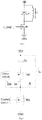
- FIG. 2 The schematic circuit block diagram of the features of the prior art is as shown in Figure 2 .
- MOS Metal Oxide Semiconductor
- TR1 Metal Oxide Semiconductor
- TR2 a fast turn-off transistor TR2 needs to be turned on to provide a freewheel loop for a contactor coil, and energy for driving quick turning off and conduction is supplied by the contactor coil.
- This technology is characterized in that in the pull-in and holding stages, after the MOS transistor TR1 is turned off, the current of the coil flows through a drive circuit; and after the fast turn-off transistor is driven to be turned on, the other current flows through the fast turn-off transistor.
- the fast turn-off transistor In the pull-in and holding stages, after the MOS transistor TR1 is turned off, the current flowing through the fast turn-off transistor and the drive circuit accords with the following relation: I L -I dri +I ds . Besides, the fast turn-off transistor also has other characteristic relations. When the fast turn-off transistor adopts an NPN triode or an MOS transistor, the relation is different.
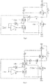
- Figure 3-1 and Figure 3-2 respectively show specific examples of the NPN triode and the MOS transistor in the prior art.
- the MOS transistor TR1 In pull-in and holding processes, the MOS transistor TR1 is turned on and turned off at a certain frequency duty ratio.
- the principle of above-the-ground MOS transistor driving is that when TR1 is turned off, current of an inductor needs to be freewheeled. As the inductance of the contactor coil is relatively high, and approximates to a constant current source, when TR1 is turned off, the coil current may find other loops for freewheeling. The coil current would first flow through the base of a triode or the gate of the MOS transistor to drive the triode or the MOS transistor to be conducted.
- the energy of the fast turn-off transistor is always supplied by freewheeling current of the contactor coil, the above-mentioned formulas are always valid, the fast turn-off transistor is always in an amplified state, the voltage drop is relatively large, and the loss of the fast turn-off transistor is also relatively high during freewheeling.
- Persons skilled in the art cannot make the fast turn-off transistor conducted in a saturated manner under a condition of requiring relatively low cost, and cannot minimize the loss in the pull-in and holding stages of the contactor.
- the fast turn-off transistors are in the amplified state all the time, with a relatively large conduction voltage drop.
- the coil current is freewheeled through a freewheel loop formed by the fast turn-off transistor and D1, and energy consumed by the freewheel loop is I L *V on .
- the fast turn-off transistor is designed on the basis of optimal loss.
- the saturated conduction voltage drop of the triode is generally 0.3 V
- the conduction resistance of the MOS transistor is selected as 0.05 ⁇
- the coil current I L is equal to 1 A, so that it is very easy to obtain the loss of 0.3 W of the triode and the loss of 0.05 W of the MOS transistor.
- the schematic circuit block diagram of a contactor coil control circuit of the present application is as shown in Figure 4 .
- a first embodiment of the contactor coil control circuit of the present application is as shown in Figure 5 .
- the contactor coil control circuit includes a switch control circuit, a drive circuit, a fast turn-off circuit, a diode D1, an MOS (Metal Oxide Semiconductor) transistor TR1 and a contactor coil L1.
- MOS Metal Oxide Semiconductor
- the fast turn-off circuit includes an MOS transistor TR2; the drive circuit includes a capacitor C1, a diode D2 and a resistor R1; and the switch control circuit includes a diode D3, an inverter U1, an MOS transistor TR3, an MOS transistor TR4, a first signal port CTRL1, a second signal port CTRL2 and a third signal port CTRL3.
- connection relation of all the devices of the first embodiment is as follows: the cathode of the diode D1 is connected to an input voltage VIN, and the anode of the diode D1 is connected to the source of the MOS transistor TR2; the drain of the MOS transistor TR2 is connected to the drain of the MOS transistor TR1; the source of the MOS transistor TR1 is grounded; one end of the contactor coil L1 is connected to the input voltage VIN, and the other end of the contactor coil L1 is connected to the drain of the MOS transistor TR1; and the gate of the MOS transistor TR1 is connected to the first signal port CTRL1.
- the capacitor C1 is connected in parallel to the gate and the source of the MOS transistor TR2; the cathode of the diode D2 is connected to the gate of the MOS transistor TR2; and the resistor R1 is connected between the anode of the diode D2 and the drain of the MOS transistor TR2.
- the drain of the MOS transistor TR4 is connected to the gate of the MOS transistor TR2; the gate of the MOS transistor TR4 is connected to the third signal port CTRL3; the source of the MOS transistor TR4 is connected to the drain of the MOS transistor TR3, and is also connected to the cathode of the diode D3; the source of the MOS transistor TR3 is grounded; the second signal port CTRL2 is connected to the anode of the diode D3 and the input end of the inverter U1 respectively; and an output of the inverter U1 is connected to the gate of the MOS transistor TR3.
- a control method of the first embodiment is as follows.
- the first signal port CTRL1 continuously outputs square wave signals to control the MOS transistor TR1 to be turned on and turned off continuously, and the third signal port CTRL3 continuously inputs low level signals to enable the MOS transistor TR4 to be turned off continuously.
- the first signal port CTRL1 does not output the square wave signals to control the MOS transistor TR1 to be turned off continuously, and the third signal port CTRL3 inputs high level signals to enable the MOS transistor TR4 to be turned on continuously.
- the second signal port CTRL2 has the characteristics that: in the contactor pull-in and holding stages, the second signal port CTRL2 is at a high level; when the MOS transistor TR1 is conducted, the current from the second signal port CTRL2 charges the capacitor C1 through a loop formed by a body diode of the MOS transistor TR4, a body diode of the MOS transistor TR2 and the MOS transistor TR1, and the voltage of the capacitor C1 is approximately equal to that of the second signal port CTRL2.
- the capacitor C1 continuously supplies power to the gate of the MOS transistor TR2, so that the MOS transistor TR2 may work in a completely saturated conduction state, with extremely low loss.
- the second signal port CTRL2 is at a low level, and controls the MOS transistor TR3 to be conducted, and the power of the capacitor C1 is quickly discharged through a loop formed by the MOS transistor TR4, the MOS transistor TR3 , a body diodes of the MOS transistor TR1 and the MOS transistor TR2 in the turn-off stage.
- the power of the contactor coil L1 is quickly consumed away by the MOS transistor TR2 to achieve a fast turn-off effect.
- the second signal port CTRL2 may be a current supply end of the capacitor C1, and in other embodiments, the current supply end of the capacitor C1 may also be an individually disposed power supply port to realize the same or similar function, namely to supply energy to the capacitor C1 to enable the voltage of the capacitor C1 to be much higher than the turn-on threshold value of the fast turn-off transistor and enable the fast turn-off transistor to be conducted in a saturated manner.
- the dash-line area in Figure 5 are all integrated in a chip, and the capacitor C1, the resistor R1 and the diode D2 are all low-power surface-mounted devices, which are extremely low in cost and extremely small in volume.
- the MOS transistors work in a completely conducted state all the time, with nearly ignorable loss.
- FIG. 6 The schematic circuit diagram of a contactor coil control circuit of a second embodiment of the present application is as shown in Figure 6 .
- the circuit and the control method are both similar to those of the first embodiment.
- a difference between this embodiment and the first embodiment is that a voltage stabilizing diode Z1 replaces the resistor R1 in the first embodiment.
- the voltage drop between the drain and the source of the MOS transistor TR2 is larger in the fast turn-off stage, so that the contactor is turned off more quickly.
- the schematic circuit diagram of a contactor coil control circuit of a third embodiment of the present application is as shown in Figure 7 .
- the circuit and the control method are both similar to those of the first embodiment.
- a difference between this embodiment and the first embodiment is that the resistor R1 in the first embodiment is not provided in this embodiment, but a power resistor R3 is connected in parallel to the drain and the source of the MOS transistor TR2.
- the working process of the circuit is the same as that of the first embodiment; and in the turn-off stage, the MOS transistor TR2 is completely turned off, and the power of the contactor coil is quickly consumed away by the power resistor R3, so that the larger the resistance value of the resistor R3 is, the quicker the contactor will be turned off.
- the schematic circuit diagram of a contactor coil control circuit of a fourth embodiment of the present application is as shown in Figure 8 .
- the contactor coil control circuit includes a switch control circuit, a drive circuit, a fast turn-off circuit, a diode D1, an MOS transistor TR1 and a contactor coil L1.
- the fast turn-off circuit includes an MOS transistor TR2;
- the drive circuit includes a capacitor C1, a resistor R4, a diode D2 and a voltage stabilizing diode Z1;
- the switch control circuit includes a diode D3, a first signal port CTRL1 and a second signal port CTRL2.
- connection relation of all the devices of the fourth embodiment is as follows: the cathode of the diode D1 is connected to an input voltage VIN, and the anode of the diode D1 is connected to the source of the MOS transistor TR2; the drain of the MOS transistor TR2 is connected to the drain of the MOS transistor TR1; the source of the MOS transistor TR1 is grounded; one end of the contactor coil L1 is connected to the input voltage VIN, and the other end of the contactor coil L1 is connected to the drain of the MOS transistor TR1; and the gate of the MOS transistor TR1 is connected to the first signal port CTRL1.
- the capacitor C1 and the resistor R4 are connected in parallel to the gate and the source of the MOS transistor TR2; and after being connected in series, the diode D2 and the voltage stabilizing diode Z1 are connected in parallel to the gate and the drain of the MOS transistor TR2.
- the cathode of the diode D3 is connected to the cathode of the diode D2, and the anode of the diode D3 is connected to the second signal port CTRL2.
- a control method of the fourth embodiment is as follows.
- the first signal port CTRL1 continuously outputs square wave signals to control the MOS transistor TR1 to be turned on and turned off continuously. In the turn-off stage, the first signal port CTRL1 does not output the square wave signals to control the MOS transistor TR1 to be turned off continuously.
- the second signal port CTRL2 has the characteristics that: in the contactor pull-in and holding stages, the second signal port CTRL2 is at a high level; when the MOS transistor TR1 is conducted, the current from the second signal port CTRL2 charges the capacitor C1 through a loop formed by the diode D3, the capacitor C1, a body diode of the MOS transistor TR2 and the MOS transistor TR1.
- the capacitor C1 continuously supplies power to the gate of the MOS transistor TR2 to enable the MOS transistor TR2 to be conducted in a saturated manner, with extremely low loss.
- the second signal port CTRL2 is at a low level, the power of the capacitor C1 is consumed away by the resistor R4, the MOS transistors work in an amplification region, and a voltage drop between the drain and the source of the MOS transistor TR2 is equal to V gs +V z .
- the contactor coil is demagnetized at a relatively high voltage, so that its power is quickly consumed away by the MOS transistors to achieve a fast turn-off effect.
- a current supply end of the capacitor C1 may be either the second signal port CTRL2 or an individually disposed power supply port.
- FIG. 9 is the schematic circuit diagram of a contactor coil control circuit of a fifth embodiment of the present application.
- the contactor coil control circuit includes a switch control circuit, a drive circuit, a fast turn-off circuit, a diode D1, an MOS transistor TR1 and a contactor coil L1.
- the fast turn-off circuit includes an MOS transistor TR2 and a resistor R3; and the drive circuit includes a capacitor C1, a diode D2, a voltage detection circuit and a logic control circuit.
- connection relation of all the devices of the fifth embodiment is as follows: the cathode of the diode D1 is connected to an input voltage VIN, and the anode of the diode D1 is connected to the source of the MOS transistor TR2; the drain of the MOS transistor TR2 is connected to the drain of the MOS transistor TR1; the resistor R3 is connected in parallel to the drain and the source of the MOS transistor; the source of the MOS transistor TR1 is grounded; and one end of the contactor coil L1 is connected to the input voltage VIN, and the other end of the contactor coil L1 is connected to the drain of the MOS transistor TR1.
- the anode of the diode D2 is connected to the drain of the MOS transistor TR1, and the cathode of the diode is connected to one end of the capacitor C1; the other end of the capacitor C1 is connected to the source of the MOS transistor TR2; the input end of the voltage detection circuit is connected to the cathode of the diode D2; the output port of the voltage detection circuit is connected to a first input port of the logic control circuit; and an output port of the logic control circuit is connected to the gate of the MOS transistor TR2.
- a first output port of the switch control circuit is connected to the gate of the MOS transistor TR1, and a second output port of the switch control circuit is connected to a second input port of the logic control circuit.
- a control method of the fifth embodiment is as follows.
- the first output port of the switch control circuit continuously outputs square wave signals to control the MOS transistor TR1 to be turned on and turned off continuously.
- the first output port of the switch control circuit does not output the square wave signals to control the MOS transistor TR1 to be turned off continuously.
- the voltage detection circuit has the control characteristics that: the voltage detection circuit detects the voltage at two ends of the capacitor C1; when the voltage at the two ends of the capacitor is higher than a threshold value VTH1, the voltage detection circuit outputs a high level; and when the voltage at the two ends of the capacitor is lower than the threshold value VTH1, the voltage detection circuit outputs a low level.
- the logic control circuit has the control characteristics that: in the pull-in and holding stages, when the voltage detection circuit outputs the low level, the logic control circuit controls the MOS transistor TR2 to be completely conducted; and when the voltage detection circuit outputs the high level, the logic control circuit controls the MOS transistor TR2 to be completely turned off to enable the freewheeling current of the contactor coil L1 to charge the capacitor C1.
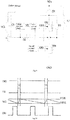
- the logic sequence of the circuit is as shown in Figure 10 .
- the voltage on the capacitor C1 is controlled by the voltage detection circuit, and may be much higher than the turn-on voltage threshold value of the gate of the MOS transistor, so that a drive voltage DR2 may enable the MOS transistor TR2 to be completely conducted, with extremely low loss.
- the capacitor C1 and the diode D2 are both low-power surface-mounted devices, and the voltage detection circuit, the logic control circuit and the switch control circuit may be integrated in one chip, so that the whole circuit is extremely low in cost and extremely small in volume.
- the schematic circuit diagram of a contactor coil control circuit of a sixth embodiment of the present application is as shown in Figure 11 .
- the contactor coil control circuit includes a switch control circuit, a drive circuit, a fast turn-off circuit, a diode D1, an MOS transistor TR1 and a contactor coil L1.
- the switch control circuit includes an MOS transistor TR3, a first signal port CTRL1 and a second signal port CTRL2; the drive circuit includes a resistor R1 and a resistor R4; and the fast turn-off circuit includes a PNP triode Q1.
- connection relation of all the devices of the sixth embodiment is as follows: the cathode of the diode D1 is connected to an input voltage VIN, and the anode of the diode D1 is connected to the collector of the PNP triode Q1; the emitter of the PNP triode Q1 is connected to the drain of the MOS transistor TR1; the source of the MOS transistor TR1 is grounded; one end of the contactor coil L1 is connected to the input voltage VIN, and the other end of the contactor coil L1 is connected to the drain of the MOS transistor TR1; and the gate of the MOS transistor TR1 is connected to the first signal port CTRL1.
- the resistor R4 is connected between the base and the collector of the PNP triode Q1; the resistor R1 is connected between the base of the PNP triode Q1 and the drain of the MOS transistor TR3; the source of the MOS transistor TR3 is grounded; and the gate of the MOS transistor TR3 is connected to the second signal port CTRL2.
- a control method of the sixth embodiment is as follows.
- the first signal port CTRL1 continuously outputs square wave signals to control the MOS transistor TR1 to be turned on and turned off continuously. In the turn-off stage, the first signal port CTRL1 does not output the square wave signals to control the MOS transistor TR1 to be turned off continuously.
- the second signal port CTRL2 has the characteristics that: in the pull-in and holding stages, the second signal port CTRL2 controls the MOS transistor TR3 to be conducted; when the MOS transistor TR1 is turned off, the current of the contactor coil may flow through the base of the PNP triode and the resistor R1 and then flow into the ground to enable the PNP triode to be conducted.
- the second signal port CTRL2 controls the MOS transistor TR2 to be turned off, and the PNP triode Q1 will work in an amplification region.
- the dash-line area in Figure 11 may be implemented by means of integrated circuits, and the resistors R1 and R4 are both low-power surface-mounted devices, which are extremely low in cost and extremely small in volume.
- the schematic circuit diagram of a contactor coil control circuit of a sixth embodiment is as shown in Figure 12 .
- the contactor coil control circuit and a control method thereof are similar to those of the sixth embodiment.
- a different between this embodiment and the seventh embodiment is that the resistor R3 is connected in parallel to the collector and the emitter of the PNP triode. In the turn-off stage, the PNP triode Q1 is completely turned off, and the current of the contactor coil is quickly discharged through R3.
- Other working principles are completely the same as those of the fifth embodiment.
- the dash-line area in Figure 12 may be implemented by means of integrated circuits, and the resistors R1 and R4 are both low-power surface-mounted devices, which are extremely low in cost and extremely small in volume.
Landscapes
- Engineering & Computer Science (AREA)
- Power Engineering (AREA)
- Physics & Mathematics (AREA)
- Electromagnetism (AREA)
- Electronic Switches (AREA)
- Relay Circuits (AREA)
- Power Conversion In General (AREA)
Applications Claiming Priority (2)
| Application Number | Priority Date | Filing Date | Title |
|---|---|---|---|
| CN201610526057.4A CN106024521B (zh) | 2016-07-05 | 2016-07-05 | 一种接触器线圈控制电路 |
| PCT/CN2016/097519 WO2018006487A1 (zh) | 2016-07-05 | 2016-08-31 | 一种接触器线圈控制电路 |
Publications (4)
| Publication Number | Publication Date |
|---|---|
| EP3401941A1 true EP3401941A1 (de) | 2018-11-14 |
| EP3401941A4 EP3401941A4 (de) | 2020-01-01 |
| EP3401941B1 EP3401941B1 (de) | 2023-06-07 |
| EP3401941C0 EP3401941C0 (de) | 2023-06-07 |
Family
ID=57108016
Family Applications (1)
| Application Number | Title | Priority Date | Filing Date |
|---|---|---|---|
| EP16907991.0A Active EP3401941B1 (de) | 2016-07-05 | 2016-08-31 | Schützspulensteuerschaltung |
Country Status (5)
| Country | Link |
|---|---|
| US (1) | US10910182B2 (de) |
| EP (1) | EP3401941B1 (de) |
| JP (1) | JP6714094B2 (de) |
| CN (1) | CN106024521B (de) |
| WO (1) | WO2018006487A1 (de) |
Cited By (1)
| Publication number | Priority date | Publication date | Assignee | Title |
|---|---|---|---|---|
| CN114220623A (zh) * | 2021-12-28 | 2022-03-22 | 安阳凯地磁力科技股份有限公司 | 一种快响应、低温升双工位防爆电磁铁 |
Families Citing this family (28)
| Publication number | Priority date | Publication date | Assignee | Title |
|---|---|---|---|---|
| CN109292561B (zh) * | 2017-07-25 | 2020-11-17 | 江苏科技大学 | 一种基于刷卡机开门并呼叫电梯和照明的电路及实现方法 |
| CN107967021B (zh) * | 2017-12-26 | 2024-06-04 | 华景传感科技(无锡)有限公司 | 一种mos管驱动电压的控制电路 |
| CN108735552B (zh) * | 2018-08-17 | 2024-01-16 | 广州金升阳科技有限公司 | 接触器的线圈控制电路 |
| CN109659194B (zh) * | 2018-12-29 | 2024-05-03 | 长城电源技术(广西)有限公司 | 一种继电器控制电路及电源 |
| CN112820585B (zh) * | 2019-11-15 | 2025-01-21 | 施耐德电器工业公司 | 接触器及其供电方法 |
| CN110867343B (zh) * | 2019-11-20 | 2021-10-22 | 广州金升阳科技有限公司 | 一种接触器线圈隔离控制电路及其隔离控制方法 |
| CN110911229A (zh) * | 2019-11-26 | 2020-03-24 | 天索(苏州)控制技术有限公司 | 具有保护功能的感性线圈驱动电路 |
| CN110931312B (zh) * | 2019-11-26 | 2022-05-20 | 广州金升阳科技有限公司 | 一种接触器节电控制方法及应用该方法的控制电路 |
| CN112233935B (zh) * | 2019-12-30 | 2022-03-29 | 蜂巢能源科技有限公司 | 接触器驱动设备及系统 |
| CN111244888B (zh) * | 2020-03-04 | 2022-12-13 | 汉中一零一航空电子设备有限公司 | 一种机载汇流条接触器无源快速关断电路及关断方法 |
| US11676786B2 (en) * | 2020-04-09 | 2023-06-13 | Rockwell Automation Technologies, Inc. | Systems and methods for controlling contactor open time |
| CN111883388B (zh) * | 2020-07-23 | 2025-06-17 | 重庆川仪自动化股份有限公司 | 一种驱动继电器快速通断的控制电路 |
| CN112087136B (zh) * | 2020-08-05 | 2024-07-19 | 广州金升阳科技有限公司 | 关断控制电路及其控制方法 |
| CN112259414B (zh) * | 2020-09-18 | 2024-06-11 | 力神(青岛)新能源有限公司 | 一种直流接触器线圈的低边驱动自保持电路 |
| CN112349545B (zh) * | 2020-10-19 | 2023-01-31 | 北京动力源科技股份有限公司 | 一种直流开关 |
| CN113161198B (zh) * | 2021-04-14 | 2025-05-06 | 东莞市中汇瑞德电子股份有限公司 | 一种节能型继电器或接触器控制电路 |
| CN113764228B (zh) * | 2021-08-30 | 2024-10-22 | 深圳南云微电子有限公司 | 一种接触器节电电路 |
| CN113965059B (zh) * | 2021-10-20 | 2023-08-11 | 深圳市英锐恩科技有限公司 | 人体触摸识别电路、方法及装置 |
| CN114220624B (zh) * | 2021-12-28 | 2023-10-27 | 安阳凯地磁力科技股份有限公司 | 快响应、低温升防爆电磁铁控制电路 |
| CN115206730A (zh) * | 2022-05-24 | 2022-10-18 | 珠海科创电力电子有限公司 | 一种加速继电器吸合的继电器驱动电路 |
| CN115224664B (zh) * | 2022-06-30 | 2024-05-14 | 山东电工电气集团新能科技有限公司 | 10kV柱上断路器CT二次侧开路的保护方法 |
| CN114866153B (zh) * | 2022-07-07 | 2022-09-16 | 国机传感科技有限公司 | 一种极低频磁传感信号发射系统、方法及装置 |
| CN116430073B (zh) * | 2022-09-23 | 2023-11-10 | 上海铁路通信有限公司 | 一种齿轮速度传感器输出频率测试电路 |
| CN115940079B (zh) * | 2022-12-16 | 2025-12-23 | 惠州市亿能电子有限公司 | 一种可快速关断mos的电路 |
| CN116403856A (zh) * | 2023-03-22 | 2023-07-07 | 大力电工襄阳股份有限公司 | 接触器驱动电路及接触器 |
| CN118431030B (zh) * | 2023-12-29 | 2025-03-14 | 成都火炬电子有限公司 | 一种自举二倍压继电器快速吸合释放的驱动电路 |
| CN119049921B (zh) * | 2024-10-28 | 2025-05-30 | 深圳戴普森新能源技术有限公司 | 一种继电器的节能控制电路 |
| CN120856112B (zh) * | 2025-07-14 | 2026-03-24 | 宁波兴为汽车电子有限公司 | N-mos管高边驱动及快速关断电路 |
Family Cites Families (28)
| Publication number | Priority date | Publication date | Assignee | Title |
|---|---|---|---|---|
| US4176388A (en) * | 1978-03-30 | 1979-11-27 | Towmotor Corporation | Control circuit for a contactor |
| US4450427A (en) * | 1981-12-21 | 1984-05-22 | General Electric Company | Contactor with flux sensor |
| CH664232A5 (de) * | 1984-05-23 | 1988-02-15 | Sodeco Compteurs De Geneve | Verfahren und schaltungsanordnung zur steuerung eines elektromagneten. |
| JPH0766733B2 (ja) * | 1985-12-14 | 1995-07-19 | 株式会社豊田自動織機製作所 | 継電器の励磁回路 |
| DE4321252C2 (de) * | 1993-06-25 | 1996-09-12 | Siemens Ag | Schaltungsanordnung zur Ansteuerung eines Schützes |
| FR2748167B1 (fr) * | 1996-04-25 | 1998-06-05 | Schneider Electric Sa | Dispositif de commande d'une charge inductive |
| JPH10335140A (ja) * | 1996-07-31 | 1998-12-18 | Matsushita Electric Works Ltd | 電磁石駆動装置 |
| EP0827170B1 (de) * | 1996-07-31 | 2004-11-03 | Matsushita Electric Works, Ltd. | Elektromagnet-Ansteuervorrichtung |
| JP3619959B2 (ja) * | 2000-10-11 | 2005-02-16 | 日本コントロール工業株式会社 | ソレノイド駆動回路 |
| CN1925085A (zh) * | 2005-09-02 | 2007-03-07 | 上海扎可电气有限公司 | 接触器宽电压节能控制器 |
| JP5373257B2 (ja) * | 2006-08-04 | 2013-12-18 | 日立オートモティブシステムズ株式会社 | エンジン用高圧ポンプ駆動回路 |
| JP2009228709A (ja) * | 2008-03-19 | 2009-10-08 | Smc Corp | 電磁弁駆動制御装置及び電磁弁の駆動制御方法 |
| JP5162335B2 (ja) * | 2008-05-30 | 2013-03-13 | 矢崎総業株式会社 | リレー制御装置 |
| US20100259861A1 (en) * | 2009-04-10 | 2010-10-14 | Pertech Resources, Inc. | Solenoid drive method that conserves power |
| CN201503817U (zh) * | 2009-07-07 | 2010-06-09 | 厦门士林电机有限公司 | 一种改进的电子式接触器控制回路 |
| CN201490100U (zh) * | 2009-08-13 | 2010-05-26 | 合肥钦力电子有限公司 | Pwm脉宽调制的接触器线圈驱动电路 |
| CN102262977B (zh) * | 2010-05-26 | 2013-10-09 | 台达电子工业股份有限公司 | 交流接触器的驱动电路 |
| US8350414B2 (en) * | 2010-08-11 | 2013-01-08 | Xantrex Technology Inc. | Semiconductor assisted DC load break contactor |
| CN202126969U (zh) * | 2011-06-23 | 2012-01-25 | 杭州和而泰智能控制技术有限公司 | 继电器驱动电路及带有该电路的装置 |
| CN102420078B (zh) * | 2012-01-04 | 2015-04-08 | 北京馨容纵横科技发展有限公司 | 用于普通电磁接触器的同步开关控制电路 |
| WO2014094830A1 (en) * | 2012-12-18 | 2014-06-26 | Siemens Aktiengesellschaft | Regulated power supply assembly for use in electrical switch |
| CN103199677B (zh) * | 2013-04-08 | 2015-08-19 | 乐金电子研发中心(上海)有限公司 | 单路隔离型mosfet驱动电路 |
| CN103560051A (zh) * | 2013-11-01 | 2014-02-05 | 威海人合机电股份有限公司 | 一种接触器控制电路 |
| CN203607339U (zh) * | 2013-12-12 | 2014-05-21 | 武汉钢铁(集团)公司 | 一种保护用继电器的控制驱动装置 |
| CN105321770B (zh) * | 2014-07-30 | 2017-09-15 | 上海电科电器科技有限公司 | 交流接触器的控制器及控制方法 |
| US10374444B2 (en) * | 2014-08-26 | 2019-08-06 | Elite Power Innovations, Llc. | Method and system for battery management |
| US9786457B2 (en) * | 2015-01-14 | 2017-10-10 | General Electric Company | Systems and methods for freewheel contactor circuits |
| CN205911239U (zh) * | 2016-07-05 | 2017-01-25 | 广州金升阳科技有限公司 | 接触器的线圈控制电路 |
-
2016
- 2016-07-05 CN CN201610526057.4A patent/CN106024521B/zh active Active
- 2016-08-31 WO PCT/CN2016/097519 patent/WO2018006487A1/zh not_active Ceased
- 2016-08-31 JP JP2018546858A patent/JP6714094B2/ja active Active
- 2016-08-31 US US16/073,804 patent/US10910182B2/en active Active
- 2016-08-31 EP EP16907991.0A patent/EP3401941B1/de active Active
Cited By (2)
| Publication number | Priority date | Publication date | Assignee | Title |
|---|---|---|---|---|
| CN114220623A (zh) * | 2021-12-28 | 2022-03-22 | 安阳凯地磁力科技股份有限公司 | 一种快响应、低温升双工位防爆电磁铁 |
| CN114220623B (zh) * | 2021-12-28 | 2023-10-27 | 安阳凯地磁力科技股份有限公司 | 一种快响应、低温升双工位防爆电磁铁 |
Also Published As
| Publication number | Publication date |
|---|---|
| CN106024521B (zh) | 2019-02-05 |
| JP2019514153A (ja) | 2019-05-30 |
| EP3401941A4 (de) | 2020-01-01 |
| US20190035583A1 (en) | 2019-01-31 |
| US10910182B2 (en) | 2021-02-02 |
| CN106024521A (zh) | 2016-10-12 |
| WO2018006487A1 (zh) | 2018-01-11 |
| EP3401941B1 (de) | 2023-06-07 |
| EP3401941C0 (de) | 2023-06-07 |
| JP6714094B2 (ja) | 2020-06-24 |
Similar Documents
| Publication | Publication Date | Title |
|---|---|---|
| EP3401941A1 (de) | Schützspulensteuerschaltung | |
| TWI523419B (zh) | 適於以脈寬調變為基礎之切換式電源的隔離型閘極驅動器 | |
| CN101431297B (zh) | 一种同步整流电路 | |
| US20220140737A1 (en) | Multi-mode control method for active clamp flyback converter | |
| CN205248774U (zh) | 一种输入防反接保护电路 | |
| CN106452040B (zh) | 启动电路 | |
| CN104795976B (zh) | 可快速关断pmos开关管的驱动控制电路的设计方法 | |
| CN102684506B (zh) | 一种提高自激推挽式变换器工作效率的方法及自激推挽式变换器 | |
| CN110112893A (zh) | 一种碳化硅半导体场效应管的驱动电路 | |
| WO2021104047A1 (zh) | 一种正反激式开关电源电路及其控制方法 | |
| CN102832793A (zh) | 功率开关管的驱动方法和装置 | |
| CN111342642A (zh) | 一种用于碳化硅mosfet驱动的反激式电源控制方法 | |
| CN207819757U (zh) | 一种启动电路 | |
| US11831307B2 (en) | Power switch drive circuit and device | |
| CN106452024A (zh) | 开关电源及单电源供电的负压驱动电路 | |
| CN201352771Y (zh) | 一种同步整流电路 | |
| CN210075089U (zh) | 一种隔离驱动电路 | |
| CN204559384U (zh) | 一种关断pmos功率器件的栅源寄生电容快速放电电路 | |
| CN219554947U (zh) | 一种低成本的mos管驱动电路 | |
| CN207399047U (zh) | 供电电压转换电路和led供电系统 | |
| CN112564480A (zh) | 一种零电流检测电路及宽负载范围的ky变换器 | |
| CN113346757A (zh) | 一种自驱动同步整流线路及其工作方法和应用 | |
| US7031463B2 (en) | Resistive feed rail generation in a power supply | |
| CN219204347U (zh) | 一种放电电路及内置放电电路的电源 | |
| CN220856480U (zh) | 一种双线圈欠压脱扣器 |
Legal Events
| Date | Code | Title | Description |
|---|---|---|---|
| STAA | Information on the status of an ep patent application or granted ep patent |
Free format text: STATUS: THE INTERNATIONAL PUBLICATION HAS BEEN MADE |
|
| PUAI | Public reference made under article 153(3) epc to a published international application that has entered the european phase |
Free format text: ORIGINAL CODE: 0009012 |
|
| STAA | Information on the status of an ep patent application or granted ep patent |
Free format text: STATUS: REQUEST FOR EXAMINATION WAS MADE |
|
| 17P | Request for examination filed |
Effective date: 20180808 |
|
| AK | Designated contracting states |
Kind code of ref document: A1 Designated state(s): AL AT BE BG CH CY CZ DE DK EE ES FI FR GB GR HR HU IE IS IT LI LT LU LV MC MK MT NL NO PL PT RO RS SE SI SK SM TR |
|
| AX | Request for extension of the european patent |
Extension state: BA ME |
|
| DAV | Request for validation of the european patent (deleted) | ||
| DAX | Request for extension of the european patent (deleted) | ||
| A4 | Supplementary search report drawn up and despatched |
Effective date: 20191203 |
|
| RIC1 | Information provided on ipc code assigned before grant |
Ipc: H01F 7/18 20060101ALI20191127BHEP Ipc: H01H 47/32 20060101AFI20191127BHEP Ipc: H01H 47/00 20060101ALI20191127BHEP Ipc: H02H 9/04 20060101ALI20191127BHEP |
|
| STAA | Information on the status of an ep patent application or granted ep patent |
Free format text: STATUS: EXAMINATION IS IN PROGRESS |
|
| 17Q | First examination report despatched |
Effective date: 20211201 |
|
| GRAP | Despatch of communication of intention to grant a patent |
Free format text: ORIGINAL CODE: EPIDOSNIGR1 |
|
| STAA | Information on the status of an ep patent application or granted ep patent |
Free format text: STATUS: GRANT OF PATENT IS INTENDED |
|
| INTG | Intention to grant announced |
Effective date: 20221122 |
|
| GRAS | Grant fee paid |
Free format text: ORIGINAL CODE: EPIDOSNIGR3 |
|
| RAP3 | Party data changed (applicant data changed or rights of an application transferred) |
Owner name: MORNSUN GUANGZHOU SCIENCE & TECHNOLOGY CO., LTD. |
|
| RAP3 | Party data changed (applicant data changed or rights of an application transferred) |
Owner name: MORNSUN GUANGZHOU SCIENCE & TECHNOLOGY CO., LTD. |
|
| RIN1 | Information on inventor provided before grant (corrected) |
Inventor name: SU, JUNXI Inventor name: TANG, SHENGBIN Inventor name: YIN, XIANGYANG |
|
| GRAA | (expected) grant |
Free format text: ORIGINAL CODE: 0009210 |
|
| STAA | Information on the status of an ep patent application or granted ep patent |
Free format text: STATUS: THE PATENT HAS BEEN GRANTED |
|
| AK | Designated contracting states |
Kind code of ref document: B1 Designated state(s): AL AT BE BG CH CY CZ DE DK EE ES FI FR GB GR HR HU IE IS IT LI LT LU LV MC MK MT NL NO PL PT RO RS SE SI SK SM TR |
|
| REG | Reference to a national code |
Ref country code: GB Ref legal event code: FG4D |
|
| REG | Reference to a national code |
Ref country code: CH Ref legal event code: EP Ref country code: AT Ref legal event code: REF Ref document number: 1577505 Country of ref document: AT Kind code of ref document: T Effective date: 20230615 |
|
| REG | Reference to a national code |
Ref country code: DE Ref legal event code: R096 Ref document number: 602016080234 Country of ref document: DE |
|
| U01 | Request for unitary effect filed |
Effective date: 20230607 |
|
| U07 | Unitary effect registered |
Designated state(s): AT BE BG DE DK EE FI FR IT LT LU LV MT NL PT SE SI Effective date: 20230612 |
|
| REG | Reference to a national code |
Ref country code: LT Ref legal event code: MG9D |
|
| U20 | Renewal fee for the european patent with unitary effect paid |
Year of fee payment: 8 Effective date: 20230830 |
|
| PG25 | Lapsed in a contracting state [announced via postgrant information from national office to epo] |
Ref country code: NO Free format text: LAPSE BECAUSE OF FAILURE TO SUBMIT A TRANSLATION OF THE DESCRIPTION OR TO PAY THE FEE WITHIN THE PRESCRIBED TIME-LIMIT Effective date: 20230907 Ref country code: ES Free format text: LAPSE BECAUSE OF FAILURE TO SUBMIT A TRANSLATION OF THE DESCRIPTION OR TO PAY THE FEE WITHIN THE PRESCRIBED TIME-LIMIT Effective date: 20230607 |
|
| PG25 | Lapsed in a contracting state [announced via postgrant information from national office to epo] |
Ref country code: RS Free format text: LAPSE BECAUSE OF FAILURE TO SUBMIT A TRANSLATION OF THE DESCRIPTION OR TO PAY THE FEE WITHIN THE PRESCRIBED TIME-LIMIT Effective date: 20230607 Ref country code: HR Free format text: LAPSE BECAUSE OF FAILURE TO SUBMIT A TRANSLATION OF THE DESCRIPTION OR TO PAY THE FEE WITHIN THE PRESCRIBED TIME-LIMIT Effective date: 20230607 Ref country code: GR Free format text: LAPSE BECAUSE OF FAILURE TO SUBMIT A TRANSLATION OF THE DESCRIPTION OR TO PAY THE FEE WITHIN THE PRESCRIBED TIME-LIMIT Effective date: 20230908 |
|
| PG25 | Lapsed in a contracting state [announced via postgrant information from national office to epo] |
Ref country code: SK Free format text: LAPSE BECAUSE OF FAILURE TO SUBMIT A TRANSLATION OF THE DESCRIPTION OR TO PAY THE FEE WITHIN THE PRESCRIBED TIME-LIMIT Effective date: 20230607 |
|
| PG25 | Lapsed in a contracting state [announced via postgrant information from national office to epo] |
Ref country code: IS Free format text: LAPSE BECAUSE OF FAILURE TO SUBMIT A TRANSLATION OF THE DESCRIPTION OR TO PAY THE FEE WITHIN THE PRESCRIBED TIME-LIMIT Effective date: 20231007 |
|
| PG25 | Lapsed in a contracting state [announced via postgrant information from national office to epo] |
Ref country code: SM Free format text: LAPSE BECAUSE OF FAILURE TO SUBMIT A TRANSLATION OF THE DESCRIPTION OR TO PAY THE FEE WITHIN THE PRESCRIBED TIME-LIMIT Effective date: 20230607 Ref country code: SK Free format text: LAPSE BECAUSE OF FAILURE TO SUBMIT A TRANSLATION OF THE DESCRIPTION OR TO PAY THE FEE WITHIN THE PRESCRIBED TIME-LIMIT Effective date: 20230607 Ref country code: RO Free format text: LAPSE BECAUSE OF FAILURE TO SUBMIT A TRANSLATION OF THE DESCRIPTION OR TO PAY THE FEE WITHIN THE PRESCRIBED TIME-LIMIT Effective date: 20230607 Ref country code: IS Free format text: LAPSE BECAUSE OF FAILURE TO SUBMIT A TRANSLATION OF THE DESCRIPTION OR TO PAY THE FEE WITHIN THE PRESCRIBED TIME-LIMIT Effective date: 20231007 Ref country code: CZ Free format text: LAPSE BECAUSE OF FAILURE TO SUBMIT A TRANSLATION OF THE DESCRIPTION OR TO PAY THE FEE WITHIN THE PRESCRIBED TIME-LIMIT Effective date: 20230607 |
|
| PG25 | Lapsed in a contracting state [announced via postgrant information from national office to epo] |
Ref country code: PL Free format text: LAPSE BECAUSE OF FAILURE TO SUBMIT A TRANSLATION OF THE DESCRIPTION OR TO PAY THE FEE WITHIN THE PRESCRIBED TIME-LIMIT Effective date: 20230607 |
|
| REG | Reference to a national code |
Ref country code: DE Ref legal event code: R097 Ref document number: 602016080234 Country of ref document: DE |
|
| PG25 | Lapsed in a contracting state [announced via postgrant information from national office to epo] |
Ref country code: MC Free format text: LAPSE BECAUSE OF FAILURE TO SUBMIT A TRANSLATION OF THE DESCRIPTION OR TO PAY THE FEE WITHIN THE PRESCRIBED TIME-LIMIT Effective date: 20230607 |
|
| REG | Reference to a national code |
Ref country code: CH Ref legal event code: PL |
|
| PG25 | Lapsed in a contracting state [announced via postgrant information from national office to epo] |
Ref country code: MC Free format text: LAPSE BECAUSE OF FAILURE TO SUBMIT A TRANSLATION OF THE DESCRIPTION OR TO PAY THE FEE WITHIN THE PRESCRIBED TIME-LIMIT Effective date: 20230607 |
|
| PLBE | No opposition filed within time limit |
Free format text: ORIGINAL CODE: 0009261 |
|
| STAA | Information on the status of an ep patent application or granted ep patent |
Free format text: STATUS: NO OPPOSITION FILED WITHIN TIME LIMIT |
|
| PG25 | Lapsed in a contracting state [announced via postgrant information from national office to epo] |
Ref country code: CH Free format text: LAPSE BECAUSE OF NON-PAYMENT OF DUE FEES Effective date: 20230831 |
|
| 26N | No opposition filed |
Effective date: 20240308 |
|
| REG | Reference to a national code |
Ref country code: IE Ref legal event code: MM4A |
|
| GBPC | Gb: european patent ceased through non-payment of renewal fee |
Effective date: 20230907 |
|
| PG25 | Lapsed in a contracting state [announced via postgrant information from national office to epo] |
Ref country code: IE Free format text: LAPSE BECAUSE OF NON-PAYMENT OF DUE FEES Effective date: 20230831 |
|
| PG25 | Lapsed in a contracting state [announced via postgrant information from national office to epo] |
Ref country code: GB Free format text: LAPSE BECAUSE OF NON-PAYMENT OF DUE FEES Effective date: 20230907 |
|
| PG25 | Lapsed in a contracting state [announced via postgrant information from national office to epo] |
Ref country code: IE Free format text: LAPSE BECAUSE OF NON-PAYMENT OF DUE FEES Effective date: 20230831 Ref country code: GB Free format text: LAPSE BECAUSE OF NON-PAYMENT OF DUE FEES Effective date: 20230907 |
|
| U20 | Renewal fee for the european patent with unitary effect paid |
Year of fee payment: 9 Effective date: 20240828 |
|
| PG25 | Lapsed in a contracting state [announced via postgrant information from national office to epo] |
Ref country code: CY Free format text: LAPSE BECAUSE OF FAILURE TO SUBMIT A TRANSLATION OF THE DESCRIPTION OR TO PAY THE FEE WITHIN THE PRESCRIBED TIME-LIMIT; INVALID AB INITIO Effective date: 20160831 |
|
| PG25 | Lapsed in a contracting state [announced via postgrant information from national office to epo] |
Ref country code: HU Free format text: LAPSE BECAUSE OF FAILURE TO SUBMIT A TRANSLATION OF THE DESCRIPTION OR TO PAY THE FEE WITHIN THE PRESCRIBED TIME-LIMIT; INVALID AB INITIO Effective date: 20160831 |
|
| U20 | Renewal fee for the european patent with unitary effect paid |
Year of fee payment: 10 Effective date: 20250827 |
|
| U1N | Appointed representative for the unitary patent procedure changed after the registration of the unitary effect |
Representative=s name: LORENZ SEIDLER GOSSEL PART. MBB; DE |
|
| PG25 | Lapsed in a contracting state [announced via postgrant information from national office to epo] |
Ref country code: TR Free format text: LAPSE BECAUSE OF FAILURE TO SUBMIT A TRANSLATION OF THE DESCRIPTION OR TO PAY THE FEE WITHIN THE PRESCRIBED TIME-LIMIT Effective date: 20230607 |