EP3402060A1 - Elektronischer wandler und zugehöriges verfahren zum betrieb eines elektronischen wandlers - Google Patents
Elektronischer wandler und zugehöriges verfahren zum betrieb eines elektronischen wandlers Download PDFInfo
- Publication number
- EP3402060A1 EP3402060A1 EP18171074.0A EP18171074A EP3402060A1 EP 3402060 A1 EP3402060 A1 EP 3402060A1 EP 18171074 A EP18171074 A EP 18171074A EP 3402060 A1 EP3402060 A1 EP 3402060A1
- Authority
- EP
- European Patent Office
- Prior art keywords
- switch
- diode
- terminal
- capacitor
- electronic
- Prior art date
- Legal status (The legal status is an assumption and is not a legal conclusion. Google has not performed a legal analysis and makes no representation as to the accuracy of the status listed.)
- Granted
Links
Images


Classifications
-
- H—ELECTRICITY
- H02—GENERATION; CONVERSION OR DISTRIBUTION OF ELECTRIC POWER
- H02M—APPARATUS FOR CONVERSION BETWEEN AC AND AC, BETWEEN AC AND DC, OR BETWEEN DC AND DC, AND FOR USE WITH MAINS OR SIMILAR POWER SUPPLY SYSTEMS; CONVERSION OF DC OR AC INPUT POWER INTO SURGE OUTPUT POWER; CONTROL OR REGULATION THEREOF
- H02M1/00—Details of apparatus for conversion
- H02M1/32—Means for protecting converters other than automatic disconnection
- H02M1/34—Snubber circuits
-
- H—ELECTRICITY
- H02—GENERATION; CONVERSION OR DISTRIBUTION OF ELECTRIC POWER
- H02M—APPARATUS FOR CONVERSION BETWEEN AC AND AC, BETWEEN AC AND DC, OR BETWEEN DC AND DC, AND FOR USE WITH MAINS OR SIMILAR POWER SUPPLY SYSTEMS; CONVERSION OF DC OR AC INPUT POWER INTO SURGE OUTPUT POWER; CONTROL OR REGULATION THEREOF
- H02M1/00—Details of apparatus for conversion
- H02M1/42—Circuits or arrangements for compensating for or adjusting power factor in converters or inverters
- H02M1/4208—Arrangements for improving power factor of AC input
- H02M1/4266—Arrangements for improving power factor of AC input using passive elements
-
- H—ELECTRICITY
- H02—GENERATION; CONVERSION OR DISTRIBUTION OF ELECTRIC POWER
- H02M—APPARATUS FOR CONVERSION BETWEEN AC AND AC, BETWEEN AC AND DC, OR BETWEEN DC AND DC, AND FOR USE WITH MAINS OR SIMILAR POWER SUPPLY SYSTEMS; CONVERSION OF DC OR AC INPUT POWER INTO SURGE OUTPUT POWER; CONTROL OR REGULATION THEREOF
- H02M3/00—Conversion of DC power input into DC power output
- H02M3/22—Conversion of DC power input into DC power output with intermediate conversion into AC
- H02M3/24—Conversion of DC power input into DC power output with intermediate conversion into AC by static converters
- H02M3/28—Conversion of DC power input into DC power output with intermediate conversion into AC by static converters using discharge tubes with control electrode or semiconductor devices with control electrode to produce the intermediate AC
- H02M3/325—Conversion of DC power input into DC power output with intermediate conversion into AC by static converters using discharge tubes with control electrode or semiconductor devices with control electrode to produce the intermediate AC using devices of a triode or a transistor type requiring continuous application of a control signal
- H02M3/335—Conversion of DC power input into DC power output with intermediate conversion into AC by static converters using discharge tubes with control electrode or semiconductor devices with control electrode to produce the intermediate AC using devices of a triode or a transistor type requiring continuous application of a control signal using semiconductor devices only
- H02M3/33538—Conversion of DC power input into DC power output with intermediate conversion into AC by static converters using discharge tubes with control electrode or semiconductor devices with control electrode to produce the intermediate AC using devices of a triode or a transistor type requiring continuous application of a control signal using semiconductor devices only of the forward type
- H02M3/33546—Conversion of DC power input into DC power output with intermediate conversion into AC by static converters using discharge tubes with control electrode or semiconductor devices with control electrode to produce the intermediate AC using devices of a triode or a transistor type requiring continuous application of a control signal using semiconductor devices only of the forward type with automatic control of the output voltage or current
- H02M3/33553—Conversion of DC power input into DC power output with intermediate conversion into AC by static converters using discharge tubes with control electrode or semiconductor devices with control electrode to produce the intermediate AC using devices of a triode or a transistor type requiring continuous application of a control signal using semiconductor devices only of the forward type with automatic control of the output voltage or current with galvanic isolation between input and output of both the power stage and the feedback loop
-
- H—ELECTRICITY
- H02—GENERATION; CONVERSION OR DISTRIBUTION OF ELECTRIC POWER
- H02M—APPARATUS FOR CONVERSION BETWEEN AC AND AC, BETWEEN AC AND DC, OR BETWEEN DC AND DC, AND FOR USE WITH MAINS OR SIMILAR POWER SUPPLY SYSTEMS; CONVERSION OF DC OR AC INPUT POWER INTO SURGE OUTPUT POWER; CONTROL OR REGULATION THEREOF
- H02M3/00—Conversion of DC power input into DC power output
- H02M3/22—Conversion of DC power input into DC power output with intermediate conversion into AC
- H02M3/24—Conversion of DC power input into DC power output with intermediate conversion into AC by static converters
- H02M3/28—Conversion of DC power input into DC power output with intermediate conversion into AC by static converters using discharge tubes with control electrode or semiconductor devices with control electrode to produce the intermediate AC
- H02M3/325—Conversion of DC power input into DC power output with intermediate conversion into AC by static converters using discharge tubes with control electrode or semiconductor devices with control electrode to produce the intermediate AC using devices of a triode or a transistor type requiring continuous application of a control signal
- H02M3/335—Conversion of DC power input into DC power output with intermediate conversion into AC by static converters using discharge tubes with control electrode or semiconductor devices with control electrode to produce the intermediate AC using devices of a triode or a transistor type requiring continuous application of a control signal using semiconductor devices only
- H02M3/33569—Conversion of DC power input into DC power output with intermediate conversion into AC by static converters using discharge tubes with control electrode or semiconductor devices with control electrode to produce the intermediate AC using devices of a triode or a transistor type requiring continuous application of a control signal using semiconductor devices only having several active switching elements
- H02M3/33571—Half-bridge at primary side of an isolation transformer
-
- H—ELECTRICITY
- H02—GENERATION; CONVERSION OR DISTRIBUTION OF ELECTRIC POWER
- H02M—APPARATUS FOR CONVERSION BETWEEN AC AND AC, BETWEEN AC AND DC, OR BETWEEN DC AND DC, AND FOR USE WITH MAINS OR SIMILAR POWER SUPPLY SYSTEMS; CONVERSION OF DC OR AC INPUT POWER INTO SURGE OUTPUT POWER; CONTROL OR REGULATION THEREOF
- H02M3/00—Conversion of DC power input into DC power output
- H02M3/22—Conversion of DC power input into DC power output with intermediate conversion into AC
- H02M3/24—Conversion of DC power input into DC power output with intermediate conversion into AC by static converters
- H02M3/28—Conversion of DC power input into DC power output with intermediate conversion into AC by static converters using discharge tubes with control electrode or semiconductor devices with control electrode to produce the intermediate AC
- H02M3/325—Conversion of DC power input into DC power output with intermediate conversion into AC by static converters using discharge tubes with control electrode or semiconductor devices with control electrode to produce the intermediate AC using devices of a triode or a transistor type requiring continuous application of a control signal
- H02M3/335—Conversion of DC power input into DC power output with intermediate conversion into AC by static converters using discharge tubes with control electrode or semiconductor devices with control electrode to produce the intermediate AC using devices of a triode or a transistor type requiring continuous application of a control signal using semiconductor devices only
- H02M3/33569—Conversion of DC power input into DC power output with intermediate conversion into AC by static converters using discharge tubes with control electrode or semiconductor devices with control electrode to produce the intermediate AC using devices of a triode or a transistor type requiring continuous application of a control signal using semiconductor devices only having several active switching elements
- H02M3/33576—Conversion of DC power input into DC power output with intermediate conversion into AC by static converters using discharge tubes with control electrode or semiconductor devices with control electrode to produce the intermediate AC using devices of a triode or a transistor type requiring continuous application of a control signal using semiconductor devices only having several active switching elements having at least one active switching element at the secondary side of an isolation transformer
-
- H—ELECTRICITY
- H02—GENERATION; CONVERSION OR DISTRIBUTION OF ELECTRIC POWER
- H02M—APPARATUS FOR CONVERSION BETWEEN AC AND AC, BETWEEN AC AND DC, OR BETWEEN DC AND DC, AND FOR USE WITH MAINS OR SIMILAR POWER SUPPLY SYSTEMS; CONVERSION OF DC OR AC INPUT POWER INTO SURGE OUTPUT POWER; CONTROL OR REGULATION THEREOF
- H02M3/00—Conversion of DC power input into DC power output
- H02M3/22—Conversion of DC power input into DC power output with intermediate conversion into AC
- H02M3/24—Conversion of DC power input into DC power output with intermediate conversion into AC by static converters
- H02M3/28—Conversion of DC power input into DC power output with intermediate conversion into AC by static converters using discharge tubes with control electrode or semiconductor devices with control electrode to produce the intermediate AC
- H02M3/325—Conversion of DC power input into DC power output with intermediate conversion into AC by static converters using discharge tubes with control electrode or semiconductor devices with control electrode to produce the intermediate AC using devices of a triode or a transistor type requiring continuous application of a control signal
- H02M3/335—Conversion of DC power input into DC power output with intermediate conversion into AC by static converters using discharge tubes with control electrode or semiconductor devices with control electrode to produce the intermediate AC using devices of a triode or a transistor type requiring continuous application of a control signal using semiconductor devices only
- H02M3/337—Conversion of DC power input into DC power output with intermediate conversion into AC by static converters using discharge tubes with control electrode or semiconductor devices with control electrode to produce the intermediate AC using devices of a triode or a transistor type requiring continuous application of a control signal using semiconductor devices only in push-pull configuration
- H02M3/3376—Conversion of DC power input into DC power output with intermediate conversion into AC by static converters using discharge tubes with control electrode or semiconductor devices with control electrode to produce the intermediate AC using devices of a triode or a transistor type requiring continuous application of a control signal using semiconductor devices only in push-pull configuration with automatic control of output voltage or current
-
- H—ELECTRICITY
- H05—ELECTRIC TECHNIQUES NOT OTHERWISE PROVIDED FOR
- H05B—ELECTRIC HEATING; ELECTRIC LIGHT SOURCES NOT OTHERWISE PROVIDED FOR; CIRCUIT ARRANGEMENTS FOR ELECTRIC LIGHT SOURCES, IN GENERAL
- H05B45/00—Circuit arrangements for operating light-emitting diodes [LED]
- H05B45/30—Driver circuits
- H05B45/37—Converter circuits
- H05B45/3725—Switched mode power supply [SMPS]
- H05B45/382—Switched mode power supply [SMPS] with galvanic isolation between input and output
-
- H—ELECTRICITY
- H05—ELECTRIC TECHNIQUES NOT OTHERWISE PROVIDED FOR
- H05B—ELECTRIC HEATING; ELECTRIC LIGHT SOURCES NOT OTHERWISE PROVIDED FOR; CIRCUIT ARRANGEMENTS FOR ELECTRIC LIGHT SOURCES, IN GENERAL
- H05B45/00—Circuit arrangements for operating light-emitting diodes [LED]
- H05B45/30—Driver circuits
- H05B45/37—Converter circuits
- H05B45/3725—Switched mode power supply [SMPS]
- H05B45/39—Circuits containing inverter bridges
-
- H—ELECTRICITY
- H05—ELECTRIC TECHNIQUES NOT OTHERWISE PROVIDED FOR
- H05B—ELECTRIC HEATING; ELECTRIC LIGHT SOURCES NOT OTHERWISE PROVIDED FOR; CIRCUIT ARRANGEMENTS FOR ELECTRIC LIGHT SOURCES, IN GENERAL
- H05B45/00—Circuit arrangements for operating light-emitting diodes [LED]
- H05B45/40—Details of LED load circuits
- H05B45/44—Details of LED load circuits with an active control inside an LED matrix
- H05B45/48—Details of LED load circuits with an active control inside an LED matrix having LEDs organised in strings and incorporating parallel shunting devices
-
- H—ELECTRICITY
- H02—GENERATION; CONVERSION OR DISTRIBUTION OF ELECTRIC POWER
- H02M—APPARATUS FOR CONVERSION BETWEEN AC AND AC, BETWEEN AC AND DC, OR BETWEEN DC AND DC, AND FOR USE WITH MAINS OR SIMILAR POWER SUPPLY SYSTEMS; CONVERSION OF DC OR AC INPUT POWER INTO SURGE OUTPUT POWER; CONTROL OR REGULATION THEREOF
- H02M1/00—Details of apparatus for conversion
- H02M1/0003—Details of control, feedback or regulation circuits
- H02M1/0029—Circuits or arrangements for limiting the slope of switching signals, e.g. slew rate
-
- H—ELECTRICITY
- H02—GENERATION; CONVERSION OR DISTRIBUTION OF ELECTRIC POWER
- H02M—APPARATUS FOR CONVERSION BETWEEN AC AND AC, BETWEEN AC AND DC, OR BETWEEN DC AND DC, AND FOR USE WITH MAINS OR SIMILAR POWER SUPPLY SYSTEMS; CONVERSION OF DC OR AC INPUT POWER INTO SURGE OUTPUT POWER; CONTROL OR REGULATION THEREOF
- H02M1/00—Details of apparatus for conversion
- H02M1/0048—Circuits or arrangements for reducing losses
- H02M1/0054—Transistor switching losses
- H02M1/0058—Transistor switching losses by employing soft switching techniques, i.e. commutation of transistors when applied voltage is zero or when current flow is zero
-
- H—ELECTRICITY
- H02—GENERATION; CONVERSION OR DISTRIBUTION OF ELECTRIC POWER
- H02M—APPARATUS FOR CONVERSION BETWEEN AC AND AC, BETWEEN AC AND DC, OR BETWEEN DC AND DC, AND FOR USE WITH MAINS OR SIMILAR POWER SUPPLY SYSTEMS; CONVERSION OF DC OR AC INPUT POWER INTO SURGE OUTPUT POWER; CONTROL OR REGULATION THEREOF
- H02M1/00—Details of apparatus for conversion
- H02M1/0064—Magnetic structures combining different functions, e.g. storage, filtering or transformation
-
- H—ELECTRICITY
- H02—GENERATION; CONVERSION OR DISTRIBUTION OF ELECTRIC POWER
- H02M—APPARATUS FOR CONVERSION BETWEEN AC AND AC, BETWEEN AC AND DC, OR BETWEEN DC AND DC, AND FOR USE WITH MAINS OR SIMILAR POWER SUPPLY SYSTEMS; CONVERSION OF DC OR AC INPUT POWER INTO SURGE OUTPUT POWER; CONTROL OR REGULATION THEREOF
- H02M3/00—Conversion of DC power input into DC power output
- H02M3/01—Resonant DC/DC converters
-
- Y—GENERAL TAGGING OF NEW TECHNOLOGICAL DEVELOPMENTS; GENERAL TAGGING OF CROSS-SECTIONAL TECHNOLOGIES SPANNING OVER SEVERAL SECTIONS OF THE IPC; TECHNICAL SUBJECTS COVERED BY FORMER USPC CROSS-REFERENCE ART COLLECTIONS [XRACs] AND DIGESTS
- Y02—TECHNOLOGIES OR APPLICATIONS FOR MITIGATION OR ADAPTATION AGAINST CLIMATE CHANGE
- Y02B—CLIMATE CHANGE MITIGATION TECHNOLOGIES RELATED TO BUILDINGS, e.g. HOUSING, HOUSE APPLIANCES OR RELATED END-USER APPLICATIONS
- Y02B20/00—Energy efficient lighting technologies, e.g. halogen lamps or gas discharge lamps
- Y02B20/30—Semiconductor lamps, e.g. solid state lamps [SSL] light emitting diodes [LED] or organic LED [OLED]
-
- Y—GENERAL TAGGING OF NEW TECHNOLOGICAL DEVELOPMENTS; GENERAL TAGGING OF CROSS-SECTIONAL TECHNOLOGIES SPANNING OVER SEVERAL SECTIONS OF THE IPC; TECHNICAL SUBJECTS COVERED BY FORMER USPC CROSS-REFERENCE ART COLLECTIONS [XRACs] AND DIGESTS
- Y02—TECHNOLOGIES OR APPLICATIONS FOR MITIGATION OR ADAPTATION AGAINST CLIMATE CHANGE
- Y02B—CLIMATE CHANGE MITIGATION TECHNOLOGIES RELATED TO BUILDINGS, e.g. HOUSING, HOUSE APPLIANCES OR RELATED END-USER APPLICATIONS
- Y02B70/00—Technologies for an efficient end-user side electric power management and consumption
- Y02B70/10—Technologies improving the efficiency by using switched-mode power supplies [SMPS], i.e. efficient power electronics conversion e.g. power factor correction or reduction of losses in power supplies or efficient standby modes
Definitions
- the description relates to electronic converters.
- Figure 1 shows a typical lighting system including an electronic converter 10 and at least one lighting module 20.
- a lighting module 20 includes one or more light radiation sources, including e.g. at least one LED (Light Emitting Diode) or other solid-state lighting means, such as e.g. laser diodes.
- LED Light Emitting Diode
- solid-state lighting means such as e.g. laser diodes.
- the electronic converter 10 is a DC/DC electronic converter. Therefore, the electronic converter 10 includes two input terminals 102a and 102b for receiving an input voltage V in and two output terminals 104a and 104b for the connection to the lighting module (s) 20.
- direct voltage V in may also be obtained from an alternated voltage (provided e.g. by the mains), e.g. via a rectification circuit, e.g. a diode-bridge rectifier, and optionally a filter, such as e.g. a capacitor connected between the terminals 102a and 102b.
- the electronic converter 10 may be either a voltage generator or a current generator, i.e. the electronic converter 10 supplies at output, via the positive terminal 104a and the negative terminal 104b, a regulated voltage V out , such as e.g. 12 or 24 VDC, or a regulated current i out .
- the lighting module 20 includes a positive input terminal 200a and a negative input terminal 200b, for the connection to the terminals 104a and 104b of the electronic converter 10.
- the lighting module 20 such as a LED module including one or more LEDs connected between the terminals 200a and 200b, may be connected, either directly or through a cable, to the electronic converter 10. Therefore, the terminal 200a is connected to the positive terminal 104a, and the terminal 200b is connected to the negative terminal 104b, and thus the lighting module receives the regulated voltage V out or the regulated current i out .
- a plurality of lighting modules 20 may be connected to the electronic converter 10.
- the lighting modules 20 may be connected in parallel to the terminals 104a and 104b.
- the lighting modules 20 are typically connected in series between the terminals 104a and 104b.
- the light emitted by the light sources of the lighting module 20 is often required to be adjustable, i.e. dimmable.
- the control circuit 112 may directly vary the amplitude of said regulated current i out as a function of a dimming control signal.
- the control circuit 112 may enable or disable the output of the electronic converter 10 as a function of a dimming control signal. In this solution, the converter 10 therefore performs the dimming operation, and regulates the average current flowing through the lighting module 20 by switching the converter 10, and therefore the lighting module 20, on or off.
- the on/off switching is often driven by means of a Pulse Width Modulation (PWM), wherein a control circuit varies the duty cycle as a function of the dimming control signal.
- PWM Pulse Width Modulation
- the PWM frequency is in the range between 100 Hz and 2 kHz.
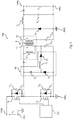
- Figure 2 shows a circuit diagram of an asymmetric electronic half-bridge converter 10.
- the electronic converter 10 therefore includes a half-bridge, i.e. two electronic switches S 1 and S 2 which are connected (typically directly) in series between the two input terminals 102a/102b, wherein the switching of the electronic switches S 1 and S 2 is driven by a control unit 112.
- said electronic switches S 1 and S 2 are n-channel Field-Effect Transistors (FETs), e.g. N-MOS, i.e. n-channel MOSFETs (Metal-Oxide-Semiconductor Field-Effect Transistors).
- FETs Field-Effect Transistors
- Said switches S 1 and S 2 may have respective capacitances C A1 , C A2 (typically the parasitic capacitances) and respective diodes D A1 , D A2 (typically the body diodes) connected in parallel thereto.
- converter 10 moreover includes a transformer T, including a primary winding T1 and a secondary winding T2.
- transformer T may be modelled as an ideal transformer having a given turns ration 1:n, an inductance L M which represents the magnetization inductance of transformer T and an inductance L R representing the leakage inductance, which are shown in Figure 2 on the primary side of transformer T.
- the primary winding of transformer T and a capacitor C RP are connected between the intermediate point between the two electronic switches S 1 /S 2 and the first input terminal 102a (positive terminal) or the second input terminal 102b (negative terminal representing a first ground GND 1 ).
- the first terminal of the primary winding T1 of transformer T is connected (e.g. directly) to the intermediate point between the two electronic switches S 1 and S 2 .
- the second terminal of the primary winding T1 of transformer T is connected via a capacitor C RP to the second input terminal 102b.
- the second terminal of the primary winding T1 of transformer T may also be connected via a further capacitor C RP to the first input terminal 102b. Therefore, the switches S 1 and S 2 may be used for selectively connecting the first terminal of the primary winding T1 of transformer T to voltage V in or to ground GND 1 , thereby controlling the current flow through the primary winding T1 of transformer T.
- the converter 10 On the secondary side T2 of transformer T, the converter 10 includes a rectification circuit, configured to convert the alternated current (AC) provided by the secondary winding T2 into a direct current (DC), and a filter circuit which stabilizes the signal provided by the rectification circuit, so that the output voltage V o and/or the output current i o are more stable.
- a rectification circuit configured to convert the alternated current (AC) provided by the secondary winding T2 into a direct current (DC), and a filter circuit which stabilizes the signal provided by the rectification circuit, so that the output voltage V o and/or the output current i o are more stable.
- the converter includes, on the secondary side of transformer T, three branches which are connected (e.g. directly) in parallel, wherein:
- a first terminal of the secondary winding T2 may be connected (e.g. directly) to the cathode of diode D, and the second terminal of the secondary winding T2 is connected (e.g. directly) via capacitor C RS to the anode of diode D.
- a first terminal of inductor L o may be connected (e.g. directly) to the cathode of diode D, and the second terminal of inductor L o may be connected (e.g. directly) via capacitor C o to the anode of diode D (which therefore represents a second ground GND 2 ).
- the electronic converter 10 is asymmetric because the on times of S 1 and S 2 are typically different, and mainly depend on the output voltage.
- the converter shown in Figure 2 offers the advantage that such a converter may be driven so as to subject switches S 1 and S 2 to Zero Voltage Switching (ZVS) and diode D may be subjected to Zero Current Switching (ZCS), so-called soft-switching.
- ZVS Zero Voltage Switching
- ZCS Zero Current Switching
- control unit 112 is typically configured to switch switches S 1 and S 2 alternatively, i.e. only one of the switches S 1 and S 2 is closed at a given time. Generally speaking, there may also be provided intermediate intervals, during which neither switch S 1 nor S 2 is closed. For this reason, the control unit 112 is typically configured to drive the switches S 1 and S 2 of the half-bridge S 1 /S 2 with the following stages, which are periodically repeated:
- Figures 3c and 3d respectively show two driver signals V GS1 and V GS2 for the gate terminals of switches S 1 and S 2
- Figure 3a shows the voltage V DS2 at the intermediate point between the switches S 1 and S 2 .
- the voltage V DS2 is equal to voltage V in
- switch S 2 is closed during the time interval ⁇ t 3
- the voltage V DS2 is zero.
- the ZVS condition may be achieved by properly sizing the resonant components of the converter (i.e. the inductances and the capacitances). Specifically, as previously mentioned, there are typically provided intermediate switching intervals ( ⁇ t 2 and ⁇ t 4) during which neither switch, S 1 or S 2 , is closed. During such intervals the current I P on the primary side of transformer T1 should charge and discharge the capacitances C A1 and C A2 associated to the switches S 1 and S 2 , so that the switches S 1 and S 2 may be closed in the following zero voltage switching stage, i.e.:
- the discharging of capacitance C A2 during time interval ⁇ t 2 may be easily ensured, because the current I P is positive at the end of interval ⁇ t 2.
- the amplitude of said current I P depends on the duration of interval ⁇ t 1, which in turn is regulated in order to achieve a desired output voltage V out or output current i out .
- the resonant components of the electronic converter 10 e.g. the transformer T, e.g. the magnetization inductance L M , may be sized so that the primary winding T1 of transformer T provides, during time interval ⁇ t 4, a negative current I P .
- the duration of time interval ⁇ t 3 should be controlled e.g. by verifying that current I P is lower than a given threshold at the end of time interval ⁇ t 3.
- the energy stored in transformer T depends therefore on the operating conditions of the electronic converter 10, e.g. the energy charged during time interval ⁇ t 1 (i.e. while switch S 1 is closed) and the output load. Therefore, the sizing of the inductances of the electronic converter 10 is typically carried out assuming the worst case. However, this also implies that the electronic converter 10 often operates in less than optimal conditions, which reduces the efficiency of converter 10. For example, details about the operation and the possible sizing of the circuit shown in Figure 2 are described in document PCT/IB2014/064657, the content whereof is incorporated herein to this end.
- the discharge of capacitance C A2 during the time interval ⁇ t 2 may be ensured easily, because the current I P is typically high during the interval ⁇ t 1.
- a capacitor may be connected (e.g. directly) in parallel with switch S 2 , so as to increase the value of capacitance C A2 .
- a high capacitance C A2 enables increasing the discharging time of capacitance C A2 , i.e. reducing the value dV / dt, thus reducing the electromagnetic interference.
- transformer T should be adapted to manage a higher amount of energy, which raises the temperature of transformer T and further reduces the efficiency of the electronic converter 10.
- the present specification aims at providing solutions which are adapted to reduce the amount of energy that the transformer is supposed to manage.
- said object is achieved thanks to an electronic converter having the features set forth in the claims that follow.
- the claims also concern a corresponding method of operating an electronic converter.
- the electronic converter includes a positive input terminal and a negative input terminal, for receiving a direct voltage, and two output terminals for providing a regulated output voltage or a regulated output current.
- at least one LED may be connected between such two output terminals.
- the electronic converter includes a half-bridge, including a first and a second electronic converter connected in series between the two input terminals, wherein a respective capacitance and a respective diode are associated with the first and the second electronic converter.
- the electronic switches may be field-effect transistors, preferably n-channel field-effect transistors, e.g. N-MOS.
- the electronic converter includes a transformer, including a primary winding and a secondary winding.
- a first terminal of the primary winding is connected to the intermediate point between the first and the second electronic switch.
- a second terminal of the primary winding is connected via a first capacitor to the positive input terminal or to the negative input terminal.
- a rectification and filter circuit is connected between the secondary circuit and the output terminals.
- the rectification and filter circuit may include:
- the first and the second electronic switch are driven by means of a control unit.
- the control unit may drive the switches according to the following time intervals, which are repeated periodically:
- the electronic converter moreover includes a snubber circuit on the primary side of the electronic converter.
- said snubber circuit includes a second capacitor, an inductor, a first diode and a second diode.
- the first terminal of the second capacitor is connected to the first terminal of the primary winding
- the second terminal of the second capacitor is connected to the cathode of the first diode
- the anode of the first diode is connected to the negative input terminal.
- the inductor and the second diode are connected in series between the cathode of the first diode and the second terminal of the primary winding, wherein the cathode of the second diode is directed towards the second terminal of the primary winding.
- the first terminal of the second capacitor is connected to the first terminal of the primary winding
- the second terminal of the second capacitor is connected to the anode of the first diode
- the cathode of the first diode is connected to the positive input terminal.
- the inductor and the second diode are connected in series between the anode of the first diode and the second terminal of the primary winding, wherein the anode of the second diode is directed towards the second terminal of the primary winding.
- the snubber circuits according to the present specification enable varying the capacitance associated to the intermediate point of the half-bridge.
- the present specification concerns an electronic converter 10a which overcomes the drawbacks of the electronic converters 10 known in the art, as described with reference to Figures 1 to 3 , i.e. asymmetric electronic half-bridge converters.
- the inventors have observed that it would be convenient for the capacitance between the intermediate point of the half-bridge (including switches S 1 and S 2 ) and ground GND 1 to vary in time.
- said capacitance should be small during the time interval ⁇ t 4 so that, at the beginning of time interval ⁇ t 4, a (negative) current I P having small amplitude may suffice to charge said capacitance, while enabling a ZVS switching of switch S 1 .
- said capacitance should be high during the time interval ⁇ t 2, so that, during time interval ⁇ t 2, the discharging time of the capacitance is prolonged, thus reducing electromagnetic interference.
- Figure 4 shows a first embodiment of an electronic converter 10a according to the present specification, which is based substantially on the circuit diagram shown in Figure 2 .
- Figure 4 only shows a capacitor C RP directly connected in series with the primary winding T1 of transformer T, between the intermediate point of the half-bridge S 1 /S 2 and ground GND 1 .
- the Figure only shows the magnetization inductance L M of transformer T.
- the electronic converter 10a receives at input, via two input terminals 102a and 102b (GND 1 ), a voltage V in , and provides at output, via two output terminals 104a and 104b, a regulated voltage V out or preferably a regulated current i out .
- a lighting module 20 may be connected to the terminals 104a and 104b (see Figure 1 ).
- the converter 10a moreover includes a half-bridge, i.e. two electronic switches S 1 and S 2 which are connected in series between the two input terminals 102a and 102b/GND 1 , wherein the switching of the electronic switches S 1 and S 2 is driven by means of a control unit 112.
- the control unit 112 may be an analog and/or digital circuit, such as e.g. a microprocessor which is programmed via software code.
- the control unit 112 is configured to drive the switches as a function of the output current i out , for example in order to regulate the output current i out to a desired (average) value.
- the electronic switches S 1 and S 2 are N-MOS transistors, i.e. n-channel MOSFETs (Metal-Oxide-Semiconductor Field-Effect Transistors). Such switches S 1 e S 2 may have, connected in parallel thereto, respective capacitances C A1 , C A2 and respective diodes D A1 , D A2 .
- the capacitances C A1 and C A2 may represent the parasitic capacitance of a MOSFET, and/or may be implemented by means of additional capacitors which are connected in parallel to the switches S 1 and S 2 .
- diodes D A1 and D A2 may represent the body diodes of a MOSFET, and/or they may be implemented by means of additional diodes.
- the converter 10a also includes a transformer T, including a primary winding T1 and a secondary winding T2.
- the electronic converter 10 may also include further inductors, which are connected in series and/or in parallel with the primary T1 and/or secondary winding T2 of transformer T.
- the first terminal of the primary winding T1 of transformer T is connected (e.g. directly) to the intermediate point between the two electronic switches S 1 and S 2 .
- the second terminal of the primary winding T1 of transformer T is connected, via a capacitor C RP , to the second input terminal 102b, i.e. to ground GND 1 .
- the switches S 1 and S 2 may be used to selectively connect the first terminal of the primary winding T1 of transformer T to voltage V in or to ground GND 1 .
- the electronic converter 10a includes, on the secondary side, three branches which are (preferably directly) connected in parallel, wherein:
- a second capacitor C o may be connected in parallel with output 104a/104b.
- Said capacitor is optional and it is used, e.g. in the case of a resistive load, for keeping the output voltage constant; however, in the case of a LED load, the voltage of the load may be constrained by the voltage of the LEDs itself, and therefore capacitor C o may also be omitted.
- a first terminal of the secondary winding T2 is connected (e.g. directly) to the cathode of diode D, and the second terminal of the secondary winding T2 is connected (e.g. directly) through capacitor C RS to the anode of diode D.
- a first terminal of inductor L o is connected (e.g. directly) to the cathode of diode D, and the second terminal of inductor L o is connected (e.g. directly) to the positive terminal of the output, and the negative terminal of the output may be connected (e.g. directly) to the anode of diode D.
- the converter is typically sized so to have a desired efficiency at the high output voltages, thus ensuring the ZVS condition for S 1 /S 2 .
- the capacitance between the intermediate point of the half-bridge (including switches S 1 and S 2 ) and ground GND 1 should be adapted to vary in time.
- said capacitance should be small during time interval ⁇ t 4, so that, at the beginning of time interval ⁇ t 4, a (negative) current I P having reduced amplitude may suffice to charge said capacitance, while enabling a ZVS switching of switch S 1 .
- said capacitance should be higher during time interval ⁇ t 2, so that, during time interval ⁇ t 2, the discharging time of the capacitance is prolonged, thereby reducing the electromagnetic interference.
- said variability of the capacitance is achieved by means of a snubber circuit 30, connected between the intermediate point of the half-bridge and ground GND 1 .
- the snubber circuit includes a capacitor C S and a diode D S which are connected in series, and a resistor R S connected in parallel with diode D S .
- this embodiment has the drawback that the current required for charging capacitor C S also flows through resistor R S , which reduces the efficiency of the electronic converter 10.
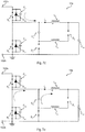
- Figure 5 shows an embodiment which overcomes said drawback.
- the snubber circuit 30 again includes a capacitor C S and a diode D 1 connected in series.
- a first terminal of capacitor C S is connected (e.g. directly) to the intermediate point of half-bridge S 1 /S 2 , i.e. the source terminal of transistor S 1 and the drain terminal of transistor S 2 , which are also connected to the first terminal of primary winding T1.
- the second terminal of capacitor C S is connected (e.g. directly) to the cathode of diode D 1 , and the anode of diode D 1 is connected (e.g. directly) to ground GND 1 , i.e. terminal 102b.
- an inductor L S and a second diode D 2 are connected (e.g. directly) between the cathode of diode D 1 and the second terminal of primary winding T 1 , which in turn is connected, via capacitor C RP , to ground GND 1 .
- the anode of diode D 2 is directed towards the cathode of diode D 1
- the cathode of diode D 2 is directed towards the second terminal of primary winding T1.
- a first terminal of inductor L S is connected (e.g. directly) to the cathode of diode D 1
- a second terminal of inductor L S is connected (e.g. directly) to the anode of diode D 2
- the cathode of diode D 2 is connected (e.g. directly) to the second terminal of primary winding T1.
- Figures 7a to 7e show different operation states of the circuit in Figure 6
- Figures 8a to 8g show some waveforms, specifically:
- the inductance of inductor L S is higher than the magnetization inductance L M of transformer T, e.g. at least twice as high, the current I CS is low and consequently the voltage V D1 at the diode D 1 substantially corresponds to the voltage V ds2 , while the voltage at capacitor V CS remains approximately zero.
- the capacitance of capacitor C S may be in the range of 1 pF - 10 nF, and the inductance of inductor L S may be in the range of 200 uH - 10 mH.
- the control unit 112 then closes switch S 1 (see Figure 7b ). Specifically, the switching may take place at zero voltage, because the voltage V ds2 is equal to voltage V in .
- the current I P increases in a substantially linear manner.
- a portion of the current is also provided to capacitor C S and to inductor L S .
- the capacitor C S and the inductor L S are in resonance.
- the voltage V CS increases and the voltage V D1 to diode D 1 decreases (see Figure 8d ).
- the voltage V CS to capacitor C S reaches a maximum value (substantially voltage V in ) and the voltage V D1 to diode D 1 becomes zero.
- the current I LS keeps on flowing through inductor L S , and therefore the diode D 1 is closed.
- the diodes D 1 and D 2 are opened, i.e. the inductor L S is coupled to ground GND 1 and to capacitor C RP only by means of the parasitic capacitances of the diodes D 1 and D 2 (see Figure 7d ).
- the electronic converter 10a behaves as a traditional electronic half-bridge converter, and the control unit 112 may open the switch S 1 at a time t 4 . Therefore, switch S 1 is closed for a time interval ⁇ t 1 (between times t 1 and t 4 ) and the control unit 112 may vary said duration in such a way as to regulate the output voltage V out or the output current i out to a desired value.
- the voltage V ds2 becomes zero, and consequently diode D 1 is opened and diode D A2 is closed, i.e. capacitance C A2 and capacitor C S remain discharged.
- the control unit 112 may close switch S 2 at zero voltage.
- the control unit 112 closes switch S 2 at a time t 6 , wherein the duration of interval ⁇ t 4 (between times t 4 and t 6 ) is constant.
- the control unit may also monitor the voltage V ds2 .
- control unit 112 may open switch S 2 at a time t ' 0 , and a new switching cycle begins.
- a new switching cycle begins.
- the capacitor C S is minimally charged in the intervals between times to and t 1 .
- the resonant components e.g. the magnetization inductance L M of transformer T
- capacitor C S is mainly charged when switch S 1 is closed and the diodes D 1 and D 2 allow the inductor L S to be completely discharged.
- capacitor C S is connected, through diode D 1 , in parallel with capacitance C A2 , thereby reducing the dV / dt ratio.
- the discharging time is increased and the electromagnetic interference is improved.
- a capacitor C RP is directly connected in series with the primary winding T1 of transformer T between the intermediate point of the half-bridge S 1 /S 2 and ground GND 1 .
- the second terminal of the primary winding T1 or transformer T might be connected via a capacitor C RP also to the first input terminal 102a.
- the primary winding T1 of transformer T and a capacitor C RP are connected in series between the intermediate point between the two electronic switches S 1 /S 2 and the first input terminal 102 (positive terminal) or the second input terminal 102b (negative terminal).
- the snubber circuit 20 may be connected to the first input terminal 102a (positive terminal) and not to the second input terminal 102b (negative terminal).
- some modifications are required. Specifically, it would be necessary to reverse also the direction of transformer T (symbolized in the drawing as a small circle) and the operation of switches S 1 and S 2 would have to be inverted. Therefore, in the presently considered embodiment, switch S 2 is connected to the first input terminal 102a (positive terminal) and switch S 1 is connected to the second input terminal 102b (negative terminal).
- the snubber circuit 30 again includes a capacitor C S and a diode D 1 connected in series.
- a first terminal of capacitor C S is connected (e.g. directly) to the intermediate point of the half-bridge S 1 /S 2 , i.e. the source terminal of transistor S 2 and the drain terminal of transistor S 1 , which are also connected to the first terminal of primary winding T1.
- the second terminal of capacitor C S is connected (e.g. directly) to the cathode of diode D 1 , and the anode of diode D 1 is connected (e.g. directly) to terminal 102a.
- an inductor L S and a second diode D 2 are connected (e.g. directly) between the anode of diode D 1 (i.e. the second terminal of capacitor C S ) and the second terminal of primary winding T1, which in turn is connected (as was previously the case) via one or more capacitors C RP to the first input terminal 102a and/or to the second input terminal 102b.
- the cathode of diode D 2 is directed towards the anode of diode D 1 (i.e. the second terminal of capacitor C S ) and the anode of diode D 2 is directed towards the second terminal of primary winding T1.
- a first terminal of inductor L S is connected (e.g. directly) to the anode of diode D 1 (i.e. the second terminal of capacitor C S ), a second terminal of inductor L S is connected (e.g. directly) to the cathode of diode D 2 and the anode of diode D 2 is connected (e.g. directly) to the second terminal of primary winding T1.
- the implementation details and the embodiments may vary, even appreciably, with respect to what has been described herein by way of non-limiting example only, without departing from the scope of the invention as defined by the annexed claims.
- the snubber circuit 30 described in the foregoing may also be used in other asymmetric electronic half-bridge converters, which make use of the magnetizing current in order to create the ZVS condition.
Landscapes
- Engineering & Computer Science (AREA)
- Power Engineering (AREA)
- Dc-Dc Converters (AREA)
Applications Claiming Priority (1)
| Application Number | Priority Date | Filing Date | Title |
|---|---|---|---|
| IT201700050228 | 2017-05-09 |
Publications (2)
| Publication Number | Publication Date |
|---|---|
| EP3402060A1 true EP3402060A1 (de) | 2018-11-14 |
| EP3402060B1 EP3402060B1 (de) | 2019-10-02 |
Family
ID=59859516
Family Applications (1)
| Application Number | Title | Priority Date | Filing Date |
|---|---|---|---|
| EP18171074.0A Active EP3402060B1 (de) | 2017-05-09 | 2018-05-07 | Elektronischer wandler und zugehöriges verfahren zum betrieb eines elektronischen wandlers |
Country Status (2)
| Country | Link |
|---|---|
| US (1) | US10243474B2 (de) |
| EP (1) | EP3402060B1 (de) |
Families Citing this family (2)
| Publication number | Priority date | Publication date | Assignee | Title |
|---|---|---|---|---|
| US12531483B2 (en) * | 2021-12-28 | 2026-01-20 | Novatek Microelectronics Corp. | Switchable power supply circuit for realizing various switching converters |
| CN114567176B (zh) * | 2022-02-15 | 2024-08-23 | 中国科学院电工研究所 | 双向直流变换器及其宽范围运行调制方法 |
Citations (4)
| Publication number | Priority date | Publication date | Assignee | Title |
|---|---|---|---|---|
| JP2001224172A (ja) * | 2000-02-09 | 2001-08-17 | Mitsubishi Electric Corp | 電力変換装置 |
| EP2395646A1 (de) * | 2009-02-06 | 2011-12-14 | Sansha Electric Manufacturing Co., Ltd. | Umrichterschaltung |
| WO2012116488A1 (en) * | 2011-03-01 | 2012-09-07 | Intersil Americas Inc. | Clamping voltage and current in an asymmetric half bridge dc/dc converter |
| WO2015044846A2 (en) * | 2013-09-25 | 2015-04-02 | Osram Gmbh | Electronic half-bridge zeta converter and related method for operating an electronic half-bridge zeta converter and method for designing an electronic half- bridge zeta converter |
Family Cites Families (2)
| Publication number | Priority date | Publication date | Assignee | Title |
|---|---|---|---|---|
| US5994848A (en) * | 1997-04-10 | 1999-11-30 | Philips Electronics North America Corporation | Triac dimmable, single stage compact flourescent lamp |
| JP6605499B2 (ja) * | 2014-04-25 | 2019-11-13 | シグニファイ ホールディング ビー ヴィ | 電力送信アンテナと一体化されたスイッチモード電源ドライバ |
-
2018
- 2018-05-07 EP EP18171074.0A patent/EP3402060B1/de active Active
- 2018-05-08 US US15/973,605 patent/US10243474B2/en active Active
Patent Citations (4)
| Publication number | Priority date | Publication date | Assignee | Title |
|---|---|---|---|---|
| JP2001224172A (ja) * | 2000-02-09 | 2001-08-17 | Mitsubishi Electric Corp | 電力変換装置 |
| EP2395646A1 (de) * | 2009-02-06 | 2011-12-14 | Sansha Electric Manufacturing Co., Ltd. | Umrichterschaltung |
| WO2012116488A1 (en) * | 2011-03-01 | 2012-09-07 | Intersil Americas Inc. | Clamping voltage and current in an asymmetric half bridge dc/dc converter |
| WO2015044846A2 (en) * | 2013-09-25 | 2015-04-02 | Osram Gmbh | Electronic half-bridge zeta converter and related method for operating an electronic half-bridge zeta converter and method for designing an electronic half- bridge zeta converter |
Also Published As
| Publication number | Publication date |
|---|---|
| US20180331629A1 (en) | 2018-11-15 |
| EP3402060B1 (de) | 2019-10-02 |
| US10243474B2 (en) | 2019-03-26 |
Similar Documents
| Publication | Publication Date | Title |
|---|---|---|
| EP3050400B1 (de) | Elektronischer resonanter und isolierter zeta-halbbrückenwandler samt steuerverfahren | |
| US10638562B2 (en) | Power converter, LED driver and control method | |
| US9787302B2 (en) | Source driver circuit and control method thereof | |
| US10116222B2 (en) | Soft switching flyback converter with primary control | |
| US9698768B2 (en) | System and method for operating a switching transistor | |
| EP2713488B1 (de) | Elektronischer Wandler und zugehöriges Beleuchtungssystem und Verfahren zum Betrieb eines elektronischen Wandlers | |
| KR101719474B1 (ko) | 적어도 하나의 반도체 광원을 동작시키기 위한 회로 어레인지먼트 | |
| US20050265057A1 (en) | Synchronous rectifier circuits and method for utilizing common source inductance of the synchronous fet | |
| US7113411B2 (en) | Switching power supply | |
| EP3365967B1 (de) | Elektronischer wandler und zugehöriges verfahren zum betrieb eines elektronischen wandlers | |
| US20050152160A1 (en) | Switching-type power converter | |
| EP3629462B1 (de) | Elektronischer umrichter und zugehöriges beleuchtungssystem und verfahren zum betrieb eines elektronischen umrichters | |
| JPWO2005076448A1 (ja) | スイッチング電源装置 | |
| US10770980B2 (en) | Electronic converter and related method of operating an electronic converter | |
| CN114600365A (zh) | 例如用于在功率因数校正中使用的逆变器电路和方法 | |
| EP3402060B1 (de) | Elektronischer wandler und zugehöriges verfahren zum betrieb eines elektronischen wandlers | |
| EP2980993B1 (de) | Betriebsgerät für eine Lichtquelle und Verfahren zum Steuern eines Betriebsgeräts | |
| EP3160028B1 (de) | Elektronischer wandler und zugehöriges verfahren zum betrieb eines elektronischen wandlers | |
| JP7760858B2 (ja) | 照明装置 | |
| Asghari et al. | A driving scheme using a single control signal for a ZVT voltage driven synchronous buck converter | |
| Ben-Yaakov et al. | A resonant local power supply with turn off snubbing features | |
| HK1060448A1 (zh) | 具有功率因数校正器的交直流变换器 |
Legal Events
| Date | Code | Title | Description |
|---|---|---|---|
| PUAI | Public reference made under article 153(3) epc to a published international application that has entered the european phase |
Free format text: ORIGINAL CODE: 0009012 |
|
| STAA | Information on the status of an ep patent application or granted ep patent |
Free format text: STATUS: THE APPLICATION HAS BEEN PUBLISHED |
|
| AK | Designated contracting states |
Kind code of ref document: A1 Designated state(s): AL AT BE BG CH CY CZ DE DK EE ES FI FR GB GR HR HU IE IS IT LI LT LU LV MC MK MT NL NO PL PT RO RS SE SI SK SM TR |
|
| AX | Request for extension of the european patent |
Extension state: BA ME |
|
| STAA | Information on the status of an ep patent application or granted ep patent |
Free format text: STATUS: REQUEST FOR EXAMINATION WAS MADE |
|
| 17P | Request for examination filed |
Effective date: 20190314 |
|
| RBV | Designated contracting states (corrected) |
Designated state(s): AL AT BE BG CH CY CZ DE DK EE ES FI FR GB GR HR HU IE IS IT LI LT LU LV MC MK MT NL NO PL PT RO RS SE SI SK SM TR |
|
| GRAP | Despatch of communication of intention to grant a patent |
Free format text: ORIGINAL CODE: EPIDOSNIGR1 |
|
| STAA | Information on the status of an ep patent application or granted ep patent |
Free format text: STATUS: GRANT OF PATENT IS INTENDED |
|
| INTG | Intention to grant announced |
Effective date: 20190510 |
|
| GRAS | Grant fee paid |
Free format text: ORIGINAL CODE: EPIDOSNIGR3 |
|
| GRAA | (expected) grant |
Free format text: ORIGINAL CODE: 0009210 |
|
| STAA | Information on the status of an ep patent application or granted ep patent |
Free format text: STATUS: THE PATENT HAS BEEN GRANTED |
|
| AK | Designated contracting states |
Kind code of ref document: B1 Designated state(s): AL AT BE BG CH CY CZ DE DK EE ES FI FR GB GR HR HU IE IS IT LI LT LU LV MC MK MT NL NO PL PT RO RS SE SI SK SM TR |
|
| REG | Reference to a national code |
Ref country code: GB Ref legal event code: FG4D |
|
| REG | Reference to a national code |
Ref country code: CH Ref legal event code: EP Ref country code: AT Ref legal event code: REF Ref document number: 1187311 Country of ref document: AT Kind code of ref document: T Effective date: 20191015 |
|
| REG | Reference to a national code |
Ref country code: DE Ref legal event code: R096 Ref document number: 602018000772 Country of ref document: DE |
|
| REG | Reference to a national code |
Ref country code: IE Ref legal event code: FG4D |
|
| REG | Reference to a national code |
Ref country code: NL Ref legal event code: MP Effective date: 20191002 |
|
| REG | Reference to a national code |
Ref country code: LT Ref legal event code: MG4D |
|
| REG | Reference to a national code |
Ref country code: AT Ref legal event code: MK05 Ref document number: 1187311 Country of ref document: AT Kind code of ref document: T Effective date: 20191002 |
|
| PG25 | Lapsed in a contracting state [announced via postgrant information from national office to epo] |
Ref country code: PT Free format text: LAPSE BECAUSE OF FAILURE TO SUBMIT A TRANSLATION OF THE DESCRIPTION OR TO PAY THE FEE WITHIN THE PRESCRIBED TIME-LIMIT Effective date: 20200203 Ref country code: AT Free format text: LAPSE BECAUSE OF FAILURE TO SUBMIT A TRANSLATION OF THE DESCRIPTION OR TO PAY THE FEE WITHIN THE PRESCRIBED TIME-LIMIT Effective date: 20191002 Ref country code: FI Free format text: LAPSE BECAUSE OF FAILURE TO SUBMIT A TRANSLATION OF THE DESCRIPTION OR TO PAY THE FEE WITHIN THE PRESCRIBED TIME-LIMIT Effective date: 20191002 Ref country code: GR Free format text: LAPSE BECAUSE OF FAILURE TO SUBMIT A TRANSLATION OF THE DESCRIPTION OR TO PAY THE FEE WITHIN THE PRESCRIBED TIME-LIMIT Effective date: 20200103 Ref country code: LT Free format text: LAPSE BECAUSE OF FAILURE TO SUBMIT A TRANSLATION OF THE DESCRIPTION OR TO PAY THE FEE WITHIN THE PRESCRIBED TIME-LIMIT Effective date: 20191002 Ref country code: BG Free format text: LAPSE BECAUSE OF FAILURE TO SUBMIT A TRANSLATION OF THE DESCRIPTION OR TO PAY THE FEE WITHIN THE PRESCRIBED TIME-LIMIT Effective date: 20200102 Ref country code: NO Free format text: LAPSE BECAUSE OF FAILURE TO SUBMIT A TRANSLATION OF THE DESCRIPTION OR TO PAY THE FEE WITHIN THE PRESCRIBED TIME-LIMIT Effective date: 20200102 Ref country code: SE Free format text: LAPSE BECAUSE OF FAILURE TO SUBMIT A TRANSLATION OF THE DESCRIPTION OR TO PAY THE FEE WITHIN THE PRESCRIBED TIME-LIMIT Effective date: 20191002 Ref country code: LV Free format text: LAPSE BECAUSE OF FAILURE TO SUBMIT A TRANSLATION OF THE DESCRIPTION OR TO PAY THE FEE WITHIN THE PRESCRIBED TIME-LIMIT Effective date: 20191002 Ref country code: NL Free format text: LAPSE BECAUSE OF FAILURE TO SUBMIT A TRANSLATION OF THE DESCRIPTION OR TO PAY THE FEE WITHIN THE PRESCRIBED TIME-LIMIT Effective date: 20191002 Ref country code: ES Free format text: LAPSE BECAUSE OF FAILURE TO SUBMIT A TRANSLATION OF THE DESCRIPTION OR TO PAY THE FEE WITHIN THE PRESCRIBED TIME-LIMIT Effective date: 20191002 Ref country code: PL Free format text: LAPSE BECAUSE OF FAILURE TO SUBMIT A TRANSLATION OF THE DESCRIPTION OR TO PAY THE FEE WITHIN THE PRESCRIBED TIME-LIMIT Effective date: 20191002 |
|
| PG25 | Lapsed in a contracting state [announced via postgrant information from national office to epo] |
Ref country code: IS Free format text: LAPSE BECAUSE OF FAILURE TO SUBMIT A TRANSLATION OF THE DESCRIPTION OR TO PAY THE FEE WITHIN THE PRESCRIBED TIME-LIMIT Effective date: 20200224 Ref country code: CZ Free format text: LAPSE BECAUSE OF FAILURE TO SUBMIT A TRANSLATION OF THE DESCRIPTION OR TO PAY THE FEE WITHIN THE PRESCRIBED TIME-LIMIT Effective date: 20191002 Ref country code: HR Free format text: LAPSE BECAUSE OF FAILURE TO SUBMIT A TRANSLATION OF THE DESCRIPTION OR TO PAY THE FEE WITHIN THE PRESCRIBED TIME-LIMIT Effective date: 20191002 Ref country code: RS Free format text: LAPSE BECAUSE OF FAILURE TO SUBMIT A TRANSLATION OF THE DESCRIPTION OR TO PAY THE FEE WITHIN THE PRESCRIBED TIME-LIMIT Effective date: 20191002 |
|
| PG25 | Lapsed in a contracting state [announced via postgrant information from national office to epo] |
Ref country code: AL Free format text: LAPSE BECAUSE OF FAILURE TO SUBMIT A TRANSLATION OF THE DESCRIPTION OR TO PAY THE FEE WITHIN THE PRESCRIBED TIME-LIMIT Effective date: 20191002 |
|
| REG | Reference to a national code |
Ref country code: DE Ref legal event code: R097 Ref document number: 602018000772 Country of ref document: DE |
|
| PG2D | Information on lapse in contracting state deleted |
Ref country code: IS |
|
| PG25 | Lapsed in a contracting state [announced via postgrant information from national office to epo] |
Ref country code: EE Free format text: LAPSE BECAUSE OF FAILURE TO SUBMIT A TRANSLATION OF THE DESCRIPTION OR TO PAY THE FEE WITHIN THE PRESCRIBED TIME-LIMIT Effective date: 20191002 Ref country code: RO Free format text: LAPSE BECAUSE OF FAILURE TO SUBMIT A TRANSLATION OF THE DESCRIPTION OR TO PAY THE FEE WITHIN THE PRESCRIBED TIME-LIMIT Effective date: 20191002 Ref country code: DK Free format text: LAPSE BECAUSE OF FAILURE TO SUBMIT A TRANSLATION OF THE DESCRIPTION OR TO PAY THE FEE WITHIN THE PRESCRIBED TIME-LIMIT Effective date: 20191002 Ref country code: IS Free format text: LAPSE BECAUSE OF FAILURE TO SUBMIT A TRANSLATION OF THE DESCRIPTION OR TO PAY THE FEE WITHIN THE PRESCRIBED TIME-LIMIT Effective date: 20200202 |
|
| PLBE | No opposition filed within time limit |
Free format text: ORIGINAL CODE: 0009261 |
|
| STAA | Information on the status of an ep patent application or granted ep patent |
Free format text: STATUS: NO OPPOSITION FILED WITHIN TIME LIMIT |
|
| PG25 | Lapsed in a contracting state [announced via postgrant information from national office to epo] |
Ref country code: SM Free format text: LAPSE BECAUSE OF FAILURE TO SUBMIT A TRANSLATION OF THE DESCRIPTION OR TO PAY THE FEE WITHIN THE PRESCRIBED TIME-LIMIT Effective date: 20191002 Ref country code: IT Free format text: LAPSE BECAUSE OF FAILURE TO SUBMIT A TRANSLATION OF THE DESCRIPTION OR TO PAY THE FEE WITHIN THE PRESCRIBED TIME-LIMIT Effective date: 20191002 Ref country code: SK Free format text: LAPSE BECAUSE OF FAILURE TO SUBMIT A TRANSLATION OF THE DESCRIPTION OR TO PAY THE FEE WITHIN THE PRESCRIBED TIME-LIMIT Effective date: 20191002 |
|
| 26N | No opposition filed |
Effective date: 20200703 |
|
| PG25 | Lapsed in a contracting state [announced via postgrant information from national office to epo] |
Ref country code: SI Free format text: LAPSE BECAUSE OF FAILURE TO SUBMIT A TRANSLATION OF THE DESCRIPTION OR TO PAY THE FEE WITHIN THE PRESCRIBED TIME-LIMIT Effective date: 20191002 |
|
| PG25 | Lapsed in a contracting state [announced via postgrant information from national office to epo] |
Ref country code: MC Free format text: LAPSE BECAUSE OF FAILURE TO SUBMIT A TRANSLATION OF THE DESCRIPTION OR TO PAY THE FEE WITHIN THE PRESCRIBED TIME-LIMIT Effective date: 20191002 |
|
| REG | Reference to a national code |
Ref country code: BE Ref legal event code: MM Effective date: 20200531 |
|
| PG25 | Lapsed in a contracting state [announced via postgrant information from national office to epo] |
Ref country code: LU Free format text: LAPSE BECAUSE OF NON-PAYMENT OF DUE FEES Effective date: 20200507 |
|
| PG25 | Lapsed in a contracting state [announced via postgrant information from national office to epo] |
Ref country code: FR Free format text: LAPSE BECAUSE OF NON-PAYMENT OF DUE FEES Effective date: 20200531 Ref country code: IE Free format text: LAPSE BECAUSE OF NON-PAYMENT OF DUE FEES Effective date: 20200507 |
|
| PG25 | Lapsed in a contracting state [announced via postgrant information from national office to epo] |
Ref country code: BE Free format text: LAPSE BECAUSE OF NON-PAYMENT OF DUE FEES Effective date: 20200531 |
|
| REG | Reference to a national code |
Ref country code: CH Ref legal event code: PL |
|
| PG25 | Lapsed in a contracting state [announced via postgrant information from national office to epo] |
Ref country code: LI Free format text: LAPSE BECAUSE OF NON-PAYMENT OF DUE FEES Effective date: 20210531 Ref country code: CH Free format text: LAPSE BECAUSE OF NON-PAYMENT OF DUE FEES Effective date: 20210531 |
|
| PG25 | Lapsed in a contracting state [announced via postgrant information from national office to epo] |
Ref country code: TR Free format text: LAPSE BECAUSE OF FAILURE TO SUBMIT A TRANSLATION OF THE DESCRIPTION OR TO PAY THE FEE WITHIN THE PRESCRIBED TIME-LIMIT Effective date: 20191002 Ref country code: MT Free format text: LAPSE BECAUSE OF FAILURE TO SUBMIT A TRANSLATION OF THE DESCRIPTION OR TO PAY THE FEE WITHIN THE PRESCRIBED TIME-LIMIT Effective date: 20191002 Ref country code: CY Free format text: LAPSE BECAUSE OF FAILURE TO SUBMIT A TRANSLATION OF THE DESCRIPTION OR TO PAY THE FEE WITHIN THE PRESCRIBED TIME-LIMIT Effective date: 20191002 |
|
| PG25 | Lapsed in a contracting state [announced via postgrant information from national office to epo] |
Ref country code: MK Free format text: LAPSE BECAUSE OF FAILURE TO SUBMIT A TRANSLATION OF THE DESCRIPTION OR TO PAY THE FEE WITHIN THE PRESCRIBED TIME-LIMIT Effective date: 20191002 |
|
| GBPC | Gb: european patent ceased through non-payment of renewal fee |
Effective date: 20220507 |
|
| PG25 | Lapsed in a contracting state [announced via postgrant information from national office to epo] |
Ref country code: GB Free format text: LAPSE BECAUSE OF NON-PAYMENT OF DUE FEES Effective date: 20220507 |
|
| PGFP | Annual fee paid to national office [announced via postgrant information from national office to epo] |
Ref country code: DE Payment date: 20250319 Year of fee payment: 8 |