EP3403239B1 - Circuit de mesure destiné à un détecteur de rayons x, procédé et système d'imagerie par rayons x correspondants - Google Patents
Circuit de mesure destiné à un détecteur de rayons x, procédé et système d'imagerie par rayons x correspondants Download PDFInfo
- Publication number
- EP3403239B1 EP3403239B1 EP16885284.6A EP16885284A EP3403239B1 EP 3403239 B1 EP3403239 B1 EP 3403239B1 EP 16885284 A EP16885284 A EP 16885284A EP 3403239 B1 EP3403239 B1 EP 3403239B1
- Authority
- EP
- European Patent Office
- Prior art keywords
- data
- measurement circuit
- detector
- measurement
- ray
- Prior art date
- Legal status (The legal status is an assumption and is not a legal conclusion. Google has not performed a legal analysis and makes no representation as to the accuracy of the status listed.)
- Active
Links
Images


Classifications
-
- A—HUMAN NECESSITIES
- A61—MEDICAL OR VETERINARY SCIENCE; HYGIENE
- A61B—DIAGNOSIS; SURGERY; IDENTIFICATION
- A61B6/00—Apparatus or devices for radiation diagnosis; Apparatus or devices for radiation diagnosis combined with radiation therapy equipment
- A61B6/02—Arrangements for diagnosis sequentially in different planes; Stereoscopic radiation diagnosis
- A61B6/03—Computed tomography [CT]
- A61B6/032—Transmission computed tomography [CT]
-
- A—HUMAN NECESSITIES
- A61—MEDICAL OR VETERINARY SCIENCE; HYGIENE
- A61B—DIAGNOSIS; SURGERY; IDENTIFICATION
- A61B6/00—Apparatus or devices for radiation diagnosis; Apparatus or devices for radiation diagnosis combined with radiation therapy equipment
- A61B6/42—Arrangements for detecting radiation specially adapted for radiation diagnosis
- A61B6/4266—Arrangements for detecting radiation specially adapted for radiation diagnosis characterised by using a plurality of detector units
-
- A—HUMAN NECESSITIES
- A61—MEDICAL OR VETERINARY SCIENCE; HYGIENE
- A61B—DIAGNOSIS; SURGERY; IDENTIFICATION
- A61B6/00—Apparatus or devices for radiation diagnosis; Apparatus or devices for radiation diagnosis combined with radiation therapy equipment
- A61B6/52—Devices using data or image processing specially adapted for radiation diagnosis
- A61B6/5205—Devices using data or image processing specially adapted for radiation diagnosis involving processing of raw data to produce diagnostic data
-
- G—PHYSICS
- G01—MEASURING; TESTING
- G01T—MEASUREMENT OF NUCLEAR OR X-RADIATION
- G01T1/00—Measuring X-radiation, gamma radiation, corpuscular radiation, or cosmic radiation
- G01T1/16—Measuring radiation intensity
- G01T1/17—Circuit arrangements not adapted to a particular type of detector
-
- G—PHYSICS
- G01—MEASURING; TESTING
- G01T—MEASUREMENT OF NUCLEAR OR X-RADIATION
- G01T1/00—Measuring X-radiation, gamma radiation, corpuscular radiation, or cosmic radiation
- G01T1/16—Measuring radiation intensity
- G01T1/24—Measuring radiation intensity with semiconductor detectors
-
- G—PHYSICS
- G06—COMPUTING OR CALCULATING; COUNTING
- G06T—IMAGE DATA PROCESSING OR GENERATION, IN GENERAL
- G06T11/00—Two-dimensional [2D] image generation
-
- G—PHYSICS
- G06—COMPUTING OR CALCULATING; COUNTING
- G06T—IMAGE DATA PROCESSING OR GENERATION, IN GENERAL
- G06T12/00—Tomographic reconstruction from projections
Definitions
- the proposed technology relates to a measurement circuit for an x-ray detector, a method for processing data by a measurement circuit of an x-ray detector prior to data read-out and an x-ray imaging system comprising a measurement circuit.
- Radiographic imaging such as x-ray imaging has been used for years in medical applications and for non-destructive testing.
- an x-ray imaging system includes an x-ray source and an x-ray detector array consisting of multiple detectors comprising one or many detector elements (independent means of measuring x-ray intensity/fluence).
- the x-ray source emits x-rays, which pass through a subject or object to be imaged and are then registered by the detector array. Since some materials absorb a larger fraction of the x-rays than others, an image is formed of the subject or object.
- An example of a commonly used x-ray imaging system is an x-ray Computed Tomography (CT) system, which may include an x-ray tube that produces a fan- or cone beam of x-rays and an opposing array of x-ray detectors measuring the fraction of x-rays that are transmitted through a patient or object.
- the x-ray tube and detector array are mounted in a gantry that rotates around the imaged object.
- An example illustration of a CT geometry is shown in FIG. 1 .
- a plurality of detector elements in the direction of the rotational axis of the gantry, i.e. the z-direction of FIG. 1 enables multi-slice image acquisition.
- a plurality of detector elements in the angular direction ( ⁇ in FIG. 1 ) enables measurement of multiple projections in the same plane simultaneously and this is applied in fan/cone-beam CT.
- Most conventional detectors are so called flat-panel detectors, meaning that they have detector elements in the slice (z) and angular ( ⁇ ) directions.
- X-ray detectors made from low-Z materials need to have a substantial thickness in the direction of the x-ray beam in order to have sufficient detection efficiency to be used in CT.
- This can be solved by, for example, using an "edge-on" geometry, as in U.S. Pat. No. 8,183,535 , in which the detector array is built up of a multitude of detectors, which comprise thin wafers of a low-atomic number material, oriented with the edge towards the impinging x-rays.
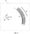
- An example illustration of a CT geometry using edge-on detectors is shown in FIG. 2 , showing the position of the source 60, the direction of the x-rays 45, the detector array 50, a single edge-on detector 5 and the angular direction of movement of the array 55. It is common that each detector has a plurality of detector elements on a 2D grid on the wafer.
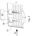
- FIG. 3 is a schematic diagram illustrating a semiconductor detector module implemented as a multi-chip module similar to an exemplary embodiment in U.S. Pat. 8,183,535 .
- the detector elements are organized in three depth segments 15 with respect to the direction of the incoming x-rays 45.
- MCM Multi-Chip Module
- the signal is routed 37 from the detector elements 15 to inputs of parallel processing circuits (e.g. ASICs) 30.
- ASIC Application Specific Integrated Circuit
- the ASIC processes the electric charge generated from each x-ray and converts it to digital data, which can be used to obtain measurement data such as a photon count and/or estimated energy.
- the ASICs are configured for connection to digital data processing circuitry 20 so the digital data may be sent to further digital data processing and/or memories located outside of the MCM and finally the data will be the input for image processing to generate a reconstructed image.
- each detector element measures the transmitted x-rays for a certain projection line. Such a measurement is called a projection measurement.
- the collection of projection measurements for many projection lines is called a sinogram.
- the sinogram data is utilized through image reconstruction to obtain an image of the interior of the imaged object.
- Each projection line (a point in the sinogram) is given by an angular coordinate, ⁇ , and a radial coordinate, r , as defined in FIG. 4 .
- Each measurement with a detector element at a specific coordinate given by ( r, ⁇ ) is a sample of the sinogram. More samples in the sinogram generally lead to a better representation of the real sinogram and therefore also a more accurately reconstructed image.
- FIG. 6A-B An example of how a detector array, similar to that displayed in FIG. 1 , samples the sinogram space is shown in FIGs. 6A-B for two different angular positions of the gantry separated by ⁇ ⁇ .
- the different r positions of the samples come from the different detectors in the array.
- a measurement period, T is here defined as the interval in time during which a certain detector element is occupied with a measurement.
- the length of the measurement period can be, but does not have to be, equal to the frame time.
- the measurement period is much smaller than the total data acquisition time and multiple measurement periods follow directly after each other throughout the overall data acquisition/measurement.
- the length of the measurement period is referred to as the temporal sampling interval and the reciprocal of the sampling interval 1/ T is referred to as the sampling frequency.
- a schematic example illustration of the angular sampling is displayed in FIG. 5 , where the detector and the source are illustrated for two different positions separated in time by the sampling interval T.
- the radial coordinate for all projection lines corresponding to a specific detector element is invariant to the rotation of the gantry.
- One way to increase the angular sampling frequency is to decrease the temporal sampling interval T . Decreasing the temporal sampling interval results in a corresponding increase in the amount of produced data.
- the temporal sampling rate can be limited by the capacity of the data transfer from the measurement circuit, rather than the measurement circuit itself.
- US Patent 5,448,609 relates to a computed tomography X-ray system, wherein the number of A/D converters required to digitize detector output signals is reduced without degrading the resultant tomographic image. This hardware reduction results from combining certain detector output signals into a pseudo detector having a single output. The detector output signals thus combined represent data corresponding to X-ray beams having substantially the same Radon radius.
- US 2015/324973 relates to a way to prevent aliasing of the X-ray detector from lowering the spatial resolution and enhance the precision of measurement in an X-ray CT device.
- An X-ray CT device for capturing an X-ray transmission image from a plurality of angular directions with respect to an object and generating a tomographic image of the object on the basis of the transmission images, wherein a plurality of detection pixels of an X-ray detector are added together and a signal is retrieved, and also the adding positions of the plurality of detection pixels are changed in synchronization with a plurality of image scanning timings, thereby allowing a computer (CPU), which is a signal processing unit, to enhance the spatial resolution without lowering the S/N of the CT image thus measured.
- CPU computer
- Another object is to provide a method for processing data by a measurement circuit of an x-ray detector prior to data read-out.
- Yet another object is to provide an x-ray imaging system comprising such a measurement circuit.
- an x-ray imaging Computed Tomography system comprising an photon-counting x-ray detector and a measurement circuit for an x-ray detector.
- the measurement circuit is configured to sample measurement data to generate data points and process the data points before read-out to produce new data points by combining two or more data points which have been acquired at different times such that the number of data points for read-out are less than the number of original data points.
- the angular sampling rate in e.g. CT is generally limited by the rate at which data can be read out from the measurement circuit of the x-ray detector.
- the measurement circuit of the detector can, however, have the capacity to sample at a higher rate than the data read-out chain can handle.
- the inventors have recognized that it may be possible that the measurement circuit can perform some operations, such as addition or multiplication, during the time between samples.
- a solution is proposed in which the data is processed in the measurement circuit before read-out. The processing may involve producing new data points by combining two or more data points which have been acquired at different times. Further, the number of data points which are read out are less than the number of original data points.
- the data points may be regarded as data samples generated by the measurement circuit when sampling measurement data.
- the measurement circuit is configured to process the data points by any combination of summation, linear combination or non-linear combination.
- the measurement circuit is configured to process data from more than one detector element of the x-ray detector.
- the measurement circuit may be configured to process data from one or more detector elements in general.
- the measurement circuit is configured to sum data from two or more detector elements before or after the signal is low-pass filtered and down-sampled.
- the measurement circuit comprises a processing unit configured to decimate the data signal from a higher sampling rate to a lower sampling rate for data read-out, while mitigating aliasing using a digital low-pass filter.
- the processing unit comprises the digital low-pass filter followed by a down-sampling module for decimating the data signal from the higher sampling rate to the lower sampling rate for data read-out.
- the measurement circuit may be configured to process electric charge generated from x-rays to obtain the measurement data.
- the measurement circuit may be configured to generate measurement data in the form of photon counts and/or estimated energy.
- the estimated energy (or equivalently charge) may be estimated photon energy and/or integrated energy.
- FIG. 9 is a schematic diagram illustrating an example of an x-ray imaging system.
- the x-ray imaging system 100 includes one or more detectors 5, each of which may have a number of detector elements, and one or more measurement circuits 30, and an image processing module 50.
- the x-ray imaging system is a Computed Tomography (CT) system.
- CT Computed Tomography
- the proposed technology involves the application of digital decimation of the signal in the measurement circuit of an x-ray detector used in CT.
- a benefit is that the proposed technology prevents aliasing artifacts in the angular (temporal) signal in CT.
- the signal is filtered using a low-pass filter and downsampled to match the requirements of the output rate.
- the higher internal sampling rate of the measurement circuit decreases the aliasing in the signal and the low-pass filter then enables downsampling without introducing aliasing; a process referred to as decimation.
- the processing includes data from several detector elements.
- the processing can include summing the data from two or more detector elements before or after the signal is low-pass filtered and downsampled.
- the pattern of how to combine the data points in order to create the new ones is stored on a memory in the measurement circuit.
- a so-called tent convolution kernel is employed as a low-pass filter
- the data new data points are formed by a linear combination of three original data points with coefficients e.g. 1 ⁇ 4, 1 ⁇ 2, 1 ⁇ 4.
- the pattern may include any combination of summation, linear combination or non-linear combination of the original, or new data points.
- the pattern can include forming new points using linear combination similar to the tent kernel described above followed by, for example, a summation of the new points formed using the tent kernel.
- FIG. 7 displays a schematic illustration of an example of a measurement setup of a detector where the measurement circuit 30 comprises a processing unit 32. Each detector element 15 of a detector may be connected individually to the measurement circuit 30.
- the measurement circuit 30 processes the electric charge generated from each x-ray and converts it to digital data, which can be used to obtain measurement data such as a photon count.
- the detector may be a photon-counting (edge-on) detector. It should though be understood that the invention is not limited thereto, and that the detector may also be a charge/energy-integrating detector.
- the measurement circuit 30 comprises one or many counters (shown in FIG. 8 ), which count the number of x-rays detected by a detector element 15 within a measurement period.
- the measurement circuit also comprises a memory 35 used for storing data during the data sampling and/or data processing.
- the measurement circuit 30 also comprises one or several processors or processing circuitries, hereinafter referred to as a processing unit 32.
- processing circuitry includes, but is not limited to, one or more microprocessors, one or more Digital Signal Processors (DSPs), one or more Central Processing Units (CPUs), video acceleration hardware, and/or any suitable programmable logic circuitry such as one or more Field Programmable Gate Arrays (FPGAs), or one or more Programmable Logic Controllers (PLCs), or Application Specific Integrated Circuitry (ASIC).
- DSPs Digital Signal Processors
- CPUs Central Processing Units
- FPGAs Field Programmable Gate Arrays
- PLCs Programmable Logic Controllers
- ASIC Application Specific Integrated Circuitry
- the measurement circuit 30 comprises one or more counters 31, a corresponding sampling module 33 for performing a sampling process, and a processing unit 32.
- the processing unit 32 comprises a digital filter 34 followed by a down-sampling module 36.
- the processing unit 32 includes the memory 35.
- the processing unit 32 is configured to decimate the signal from a higher sampling rate in the measurement circuit to a lower sampling rate for data read-out, while mitigating aliasing in the signal using a low-pass digital filter, as previously described.
- At least some of the steps, functions, procedures, and/or blocks described herein may be implemented in software such as a computer program for execution by suitable processing circuitry such as one or more processors or processing units.
- embodiments may be implemented in hardware, or in software for execution by suitable processing circuitry, or a combination thereof.
Landscapes
- Health & Medical Sciences (AREA)
- Life Sciences & Earth Sciences (AREA)
- Engineering & Computer Science (AREA)
- Medical Informatics (AREA)
- Physics & Mathematics (AREA)
- High Energy & Nuclear Physics (AREA)
- Molecular Biology (AREA)
- Surgery (AREA)
- Biomedical Technology (AREA)
- Veterinary Medicine (AREA)
- Biophysics (AREA)
- Public Health (AREA)
- Nuclear Medicine, Radiotherapy & Molecular Imaging (AREA)
- Optics & Photonics (AREA)
- Pathology (AREA)
- Radiology & Medical Imaging (AREA)
- General Health & Medical Sciences (AREA)
- Heart & Thoracic Surgery (AREA)
- Animal Behavior & Ethology (AREA)
- General Physics & Mathematics (AREA)
- Theoretical Computer Science (AREA)
- Spectroscopy & Molecular Physics (AREA)
- Pulmonology (AREA)
- Computer Vision & Pattern Recognition (AREA)
- Apparatus For Radiation Diagnosis (AREA)
- Analysing Materials By The Use Of Radiation (AREA)
Claims (5)
- Système de tomodensitométrie, CT, à imagerie radiographique (100) comprenant un détecteur de rayons X (5) et un circuit de mesure (30), dans lequel le détecteur de rayons X (5) comprend un nombre d'éléments de détecteur (15), et le circuit de mesure (30) est configuré pour être relié aux éléments de détecteur (15),dans lequel le circuit de mesure comprend un ou plusieurs compteurs de photons (31) pour compter, à l'intérieur d'une période de mesure correspondant à un intervalle d'échantillonnage temporel, le nombre de rayons X détectés pour générer des données de mesure sous la forme de comptes de photons et/ou d'une énergie photonique estimée et un module d'échantillonnage (33) correspondant relié aux compteurs de photons (31) pour réaliser un processus d'échantillonnage pour échantillonner lesdites données de mesure sous la forme de comptes de photons et/ou d'une énergie photonique estimée pour générer des points de données, etdans lequel le circuit de mesure (30) est configuré pour traiter les points de données avant de les lire pour produire de nouveaux points de données par la combinaison de deux points données ou plus qui ont été acquis à des temps différents de sorte que le nombre de points de données à lire soit inférieur au nombre de points de données initiaux,dans lequel le circuit de mesure (30) comprend une mémoire (35) pour stocker des données pendant l'échantillonnage de données et/ou le traitement de données,dans lequel le circuit de mesure (30) comprend une unité de traitement (32), ladite unité de traitement (32) comprenant un filtre passe-bas numérique (34) et un module de sous-échantillonnage (36), ladite unité de traitement (32) étant configurée pour décimer le signal de données d'un taux d'échantillonnage supérieur à un taux d'échantillonnage inférieur pour des données lues en utilisant ledit module de sous-échantillonnage (36), tout en atténuant le crénelage en utilisant ledit filtre passe-bas numérique (34) pour un filtrage anticrénelage par convolution suivi d'un sous-échantillonnage avant lecture pour empêcher des artefacts de crénelage dans le signal angulaire du système CT.
- Système CT à imagerie radiographique (100) selon la revendication 1, dans lequel le circuit de mesure (30) est configuré pour traiter les points de données par toute combinaison de sommation, combinaison linéaire ou combinaison non linéaire.
- Système CT à imagerie radiographique (100) selon la revendication 1 ou 2, dans lequel le circuit de mesure (30) est configuré pour traiter des données depuis plus d'un élément de détecteur (15) du détecteur de rayons X (5).
- Système CT à imagerie radiographique (100) selon la revendication 3, dans lequel le circuit de mesure (30) est configuré pour sommer des données provenant de deux éléments de détecteur (15) ou plus avant ou après que le signal est filtré passe-bas et sous-échantillonné.
- Système CT à imagerie radiographique (100) selon l'une quelconque des revendications 1 à 4, dans lequel le circuit de mesure (30) est configuré pour traiter une charge électrique générée à partir de rayons X pour obtenir les données de mesure.
Applications Claiming Priority (2)
| Application Number | Priority Date | Filing Date | Title |
|---|---|---|---|
| US201662278736P | 2016-01-14 | 2016-01-14 | |
| PCT/SE2016/050389 WO2017123128A1 (fr) | 2016-01-14 | 2016-05-03 | Circuit de mesure destiné à un détecteur de rayons x, procédé et système d'imagerie par rayons x correspondants |
Publications (3)
| Publication Number | Publication Date |
|---|---|
| EP3403239A1 EP3403239A1 (fr) | 2018-11-21 |
| EP3403239A4 EP3403239A4 (fr) | 2019-09-04 |
| EP3403239B1 true EP3403239B1 (fr) | 2023-07-12 |
Family
ID=59312201
Family Applications (1)
| Application Number | Title | Priority Date | Filing Date |
|---|---|---|---|
| EP16885284.6A Active EP3403239B1 (fr) | 2016-01-14 | 2016-05-03 | Circuit de mesure destiné à un détecteur de rayons x, procédé et système d'imagerie par rayons x correspondants |
Country Status (6)
| Country | Link |
|---|---|
| US (1) | US10247833B2 (fr) |
| EP (1) | EP3403239B1 (fr) |
| JP (1) | JP6710759B2 (fr) |
| KR (1) | KR102539407B1 (fr) |
| CN (1) | CN109196560B (fr) |
| WO (1) | WO2017123128A1 (fr) |
Families Citing this family (2)
| Publication number | Priority date | Publication date | Assignee | Title |
|---|---|---|---|---|
| US12471877B2 (en) * | 2022-06-07 | 2025-11-18 | GE Precision Healthcare LLC | Photon counting computed tomography (PCCT) detector sensor repair for increased sensor yield |
| US12601694B2 (en) * | 2023-08-09 | 2026-04-14 | GE Precision Healthcare LLC | System and method for improved data handling in a computed tomography imaging system |
Family Cites Families (24)
| Publication number | Priority date | Publication date | Assignee | Title |
|---|---|---|---|---|
| US5448609A (en) * | 1992-06-26 | 1995-09-05 | Siemens Aktiengesellschaft | Method and apparatus for combining CT scanner system detector outputs |
| US5724037A (en) * | 1995-05-23 | 1998-03-03 | Analog Devices, Inc. | Data acquisition system for computed tomography scanning and related applications |
| US5841829A (en) * | 1997-05-13 | 1998-11-24 | Analogic Corporation | Optimal channel filter for CT system with wobbling focal spot |
| US6963631B2 (en) * | 2002-10-25 | 2005-11-08 | Koninklijke Philips Electronics N.V. | Dynamic detector interlacing for computed tomography |
| US7136450B2 (en) * | 2004-05-26 | 2006-11-14 | Analogic Corporation | Method of and system for adaptive scatter correction in multi-energy computed tomography |
| US8290222B2 (en) * | 2006-08-29 | 2012-10-16 | Siemens Medical Solutions Usa, Inc. | Systems and methods of image processing utilizing resizing of data |
| WO2008072175A1 (fr) * | 2006-12-15 | 2008-06-19 | Koninklijke Philips Electronics N.V. | Dispositif d'imagerie à rayons x à résolution spectrale |
| US8045781B2 (en) * | 2007-07-10 | 2011-10-25 | Kabushiki Kaisha Toshiba | X-ray computed tomography apparatus, reconstruction processing apparatus, and image processing apparatus |
| WO2009038559A1 (fr) * | 2007-09-19 | 2009-03-26 | Thomson Licensing | Système et procédé de changement d'échelle d'images |
| DE102009051635A1 (de) * | 2009-11-02 | 2011-05-05 | Siemens Aktiengesellschaft | Verbesserte Streustrahlkorrektur auf Rohdatenbasis bei der Computertomographie |
| US8692708B2 (en) * | 2010-03-30 | 2014-04-08 | Sony Corporation | Radiometric imaging device and corresponding method |
| US9949718B2 (en) * | 2010-07-12 | 2018-04-24 | General Electric Company | Method and system for controlling communication of data via digital demodulation in a diagnostic ultrasound system |
| JP6200428B2 (ja) * | 2011-12-19 | 2017-09-20 | コーニンクレッカ フィリップス エヌ ヴェKoninklijke Philips N.V. | X線検出器、x線装置、プロセッサ、コンピュータプログラム、及びその関連方法 |
| US20130202085A1 (en) * | 2012-02-03 | 2013-08-08 | General Electric Company | System and method for autonomous exposure detection by digital x-ray detector |
| EP2664280A3 (fr) * | 2012-05-14 | 2013-12-04 | Samsung Electronics Co., Ltd | Appareil dýimagerie à rayons X et son procédé de contrôle |
| WO2013191001A1 (fr) * | 2012-06-20 | 2013-12-27 | 株式会社日立メディコ | Dispositif de tdm à rayons x |
| US8958660B2 (en) * | 2012-06-22 | 2015-02-17 | General Electric Company | Method and apparatus for iterative reconstruction |
| CN102937599B (zh) * | 2012-10-25 | 2015-01-07 | 中国科学院自动化研究所 | 一种通过x射线检测含金属被测物的无损检测系统和方法 |
| US9892812B2 (en) * | 2012-10-30 | 2018-02-13 | California Institute Of Technology | Fourier ptychographic x-ray imaging systems, devices, and methods |
| US8823572B2 (en) * | 2012-12-17 | 2014-09-02 | Dust Networks, Inc. | Anti-aliasing sampling circuits and analog-to-digital converter |
| JP6109560B2 (ja) * | 2012-12-21 | 2017-04-05 | 東芝メディカルシステムズ株式会社 | X線コンピュータ断層撮影装置 |
| GB201302887D0 (en) * | 2013-02-19 | 2013-04-03 | Optos Plc | Improvements in or relating to image processing |
| CN104121985B (zh) * | 2013-04-29 | 2020-07-14 | 艾默生电气(美国)控股公司(智利)有限公司 | 过采样数据的选择性抽取和分析 |
| WO2014196479A1 (fr) * | 2013-06-06 | 2014-12-11 | 株式会社 東芝 | Dispositif de comptage de photons |
-
2016
- 2016-05-03 KR KR1020187013935A patent/KR102539407B1/ko active Active
- 2016-05-03 CN CN201680065625.3A patent/CN109196560B/zh active Active
- 2016-05-03 WO PCT/SE2016/050389 patent/WO2017123128A1/fr not_active Ceased
- 2016-05-03 EP EP16885284.6A patent/EP3403239B1/fr active Active
- 2016-05-03 JP JP2018530546A patent/JP6710759B2/ja active Active
- 2016-05-03 US US15/505,374 patent/US10247833B2/en active Active
Non-Patent Citations (1)
| Title |
|---|
| YVEBORG MOA ET AL: "Photon-counting CT with silicon detectors: feasibility for pediatric imaging", PROCEEDINGS OF SPIE, vol. 7258, 26 February 2009 (2009-02-26), Orlando, Florida, pages 725825, XP055805186, ISSN: 0277-786X, ISBN: 978-1-5106-4059-7, DOI: 10.1117/12.813733 * |
Also Published As
| Publication number | Publication date |
|---|---|
| KR20180103041A (ko) | 2018-09-18 |
| KR102539407B1 (ko) | 2023-06-01 |
| JP2019503215A (ja) | 2019-02-07 |
| WO2017123128A1 (fr) | 2017-07-20 |
| US20180217277A1 (en) | 2018-08-02 |
| EP3403239A4 (fr) | 2019-09-04 |
| US10247833B2 (en) | 2019-04-02 |
| CN109196560A (zh) | 2019-01-11 |
| EP3403239A1 (fr) | 2018-11-21 |
| JP6710759B2 (ja) | 2020-06-17 |
| CN109196560B (zh) | 2023-07-04 |
Similar Documents
| Publication | Publication Date | Title |
|---|---|---|
| EP3035038B1 (fr) | Tomographie haute résolution assistée par ordinateur | |
| EP3374803B1 (fr) | Tomodensitométrie haute résolution utilisant des détecteurs de bord avec des segments de profondeur temporellement décalés | |
| JP6280544B2 (ja) | X線エネルギー別画像再構成装置及び方法並びにx線三次元測定装置及び方法 | |
| EP3353575A1 (fr) | Détermination de l'orientation d'un détecteur de rayons x à géométrie « edge-on » par rapport à la direction de rayons x entrants | |
| US8492762B2 (en) | Electrical interface for a sensor array | |
| JP2019020334A (ja) | 波高頻度分布取得装置、波高頻度分布取得方法、波高頻度分布取得プログラム及び放射線撮像装置 | |
| EP3403239B1 (fr) | Circuit de mesure destiné à un détecteur de rayons x, procédé et système d'imagerie par rayons x correspondants | |
| JP2535762B2 (ja) | 陽電子断層撮影装置におけるγ線吸収体による散乱同時計数測定法及び陽電子断層撮影装置 | |
| US20080068815A1 (en) | Interface Assembly And Method for Integrating A Data Acquisition System on a Sensor Array | |
| US10130313B2 (en) | Data acquisition for computed tomography | |
| US10048390B2 (en) | Detector implementations for X-ray detectors | |
| CN109567849B (zh) | 正电子发射ct成像仪 |
Legal Events
| Date | Code | Title | Description |
|---|---|---|---|
| STAA | Information on the status of an ep patent application or granted ep patent |
Free format text: STATUS: THE INTERNATIONAL PUBLICATION HAS BEEN MADE |
|
| PUAI | Public reference made under article 153(3) epc to a published international application that has entered the european phase |
Free format text: ORIGINAL CODE: 0009012 |
|
| STAA | Information on the status of an ep patent application or granted ep patent |
Free format text: STATUS: REQUEST FOR EXAMINATION WAS MADE |
|
| 17P | Request for examination filed |
Effective date: 20180814 |
|
| AK | Designated contracting states |
Kind code of ref document: A1 Designated state(s): AL AT BE BG CH CY CZ DE DK EE ES FI FR GB GR HR HU IE IS IT LI LT LU LV MC MK MT NL NO PL PT RO RS SE SI SK SM TR |
|
| AX | Request for extension of the european patent |
Extension state: BA ME |
|
| DAV | Request for validation of the european patent (deleted) | ||
| DAX | Request for extension of the european patent (deleted) | ||
| A4 | Supplementary search report drawn up and despatched |
Effective date: 20190805 |
|
| RIC1 | Information provided on ipc code assigned before grant |
Ipc: G01T 1/24 20060101ALI20190730BHEP Ipc: G01T 1/17 20060101ALI20190730BHEP Ipc: A61B 6/00 20060101ALI20190730BHEP Ipc: G06T 11/00 20060101AFI20190730BHEP |
|
| STAA | Information on the status of an ep patent application or granted ep patent |
Free format text: STATUS: EXAMINATION IS IN PROGRESS |
|
| 17Q | First examination report despatched |
Effective date: 20200630 |
|
| GRAP | Despatch of communication of intention to grant a patent |
Free format text: ORIGINAL CODE: EPIDOSNIGR1 |
|
| STAA | Information on the status of an ep patent application or granted ep patent |
Free format text: STATUS: GRANT OF PATENT IS INTENDED |
|
| INTG | Intention to grant announced |
Effective date: 20230210 |
|
| GRAS | Grant fee paid |
Free format text: ORIGINAL CODE: EPIDOSNIGR3 |
|
| GRAA | (expected) grant |
Free format text: ORIGINAL CODE: 0009210 |
|
| STAA | Information on the status of an ep patent application or granted ep patent |
Free format text: STATUS: THE PATENT HAS BEEN GRANTED |
|
| AK | Designated contracting states |
Kind code of ref document: B1 Designated state(s): AL AT BE BG CH CY CZ DE DK EE ES FI FR GB GR HR HU IE IS IT LI LT LU LV MC MK MT NL NO PL PT RO RS SE SI SK SM TR |
|
| P01 | Opt-out of the competence of the unified patent court (upc) registered |
Effective date: 20230528 |
|
| REG | Reference to a national code |
Ref country code: CH Ref legal event code: EP |
|
| REG | Reference to a national code |
Ref country code: IE Ref legal event code: FG4D |
|
| REG | Reference to a national code |
Ref country code: DE Ref legal event code: R096 Ref document number: 602016081064 Country of ref document: DE |
|
| REG | Reference to a national code |
Ref country code: NL Ref legal event code: FP |
|
| REG | Reference to a national code |
Ref country code: LT Ref legal event code: MG9D |
|
| REG | Reference to a national code |
Ref country code: AT Ref legal event code: MK05 Ref document number: 1587938 Country of ref document: AT Kind code of ref document: T Effective date: 20230712 |
|
| PG25 | Lapsed in a contracting state [announced via postgrant information from national office to epo] |
Ref country code: GR Free format text: LAPSE BECAUSE OF FAILURE TO SUBMIT A TRANSLATION OF THE DESCRIPTION OR TO PAY THE FEE WITHIN THE PRESCRIBED TIME-LIMIT Effective date: 20231013 |
|
| PG25 | Lapsed in a contracting state [announced via postgrant information from national office to epo] |
Ref country code: ES Free format text: LAPSE BECAUSE OF FAILURE TO SUBMIT A TRANSLATION OF THE DESCRIPTION OR TO PAY THE FEE WITHIN THE PRESCRIBED TIME-LIMIT Effective date: 20230712 |
|
| PG25 | Lapsed in a contracting state [announced via postgrant information from national office to epo] |
Ref country code: IS Free format text: LAPSE BECAUSE OF FAILURE TO SUBMIT A TRANSLATION OF THE DESCRIPTION OR TO PAY THE FEE WITHIN THE PRESCRIBED TIME-LIMIT Effective date: 20231112 |
|
| PG25 | Lapsed in a contracting state [announced via postgrant information from national office to epo] |
Ref country code: SE Free format text: LAPSE BECAUSE OF FAILURE TO SUBMIT A TRANSLATION OF THE DESCRIPTION OR TO PAY THE FEE WITHIN THE PRESCRIBED TIME-LIMIT Effective date: 20230712 Ref country code: RS Free format text: LAPSE BECAUSE OF FAILURE TO SUBMIT A TRANSLATION OF THE DESCRIPTION OR TO PAY THE FEE WITHIN THE PRESCRIBED TIME-LIMIT Effective date: 20230712 Ref country code: PT Free format text: LAPSE BECAUSE OF FAILURE TO SUBMIT A TRANSLATION OF THE DESCRIPTION OR TO PAY THE FEE WITHIN THE PRESCRIBED TIME-LIMIT Effective date: 20231113 Ref country code: NO Free format text: LAPSE BECAUSE OF FAILURE TO SUBMIT A TRANSLATION OF THE DESCRIPTION OR TO PAY THE FEE WITHIN THE PRESCRIBED TIME-LIMIT Effective date: 20231012 Ref country code: LV Free format text: LAPSE BECAUSE OF FAILURE TO SUBMIT A TRANSLATION OF THE DESCRIPTION OR TO PAY THE FEE WITHIN THE PRESCRIBED TIME-LIMIT Effective date: 20230712 Ref country code: LT Free format text: LAPSE BECAUSE OF FAILURE TO SUBMIT A TRANSLATION OF THE DESCRIPTION OR TO PAY THE FEE WITHIN THE PRESCRIBED TIME-LIMIT Effective date: 20230712 Ref country code: IS Free format text: LAPSE BECAUSE OF FAILURE TO SUBMIT A TRANSLATION OF THE DESCRIPTION OR TO PAY THE FEE WITHIN THE PRESCRIBED TIME-LIMIT Effective date: 20231112 Ref country code: HR Free format text: LAPSE BECAUSE OF FAILURE TO SUBMIT A TRANSLATION OF THE DESCRIPTION OR TO PAY THE FEE WITHIN THE PRESCRIBED TIME-LIMIT Effective date: 20230712 Ref country code: GR Free format text: LAPSE BECAUSE OF FAILURE TO SUBMIT A TRANSLATION OF THE DESCRIPTION OR TO PAY THE FEE WITHIN THE PRESCRIBED TIME-LIMIT Effective date: 20231013 Ref country code: FI Free format text: LAPSE BECAUSE OF FAILURE TO SUBMIT A TRANSLATION OF THE DESCRIPTION OR TO PAY THE FEE WITHIN THE PRESCRIBED TIME-LIMIT Effective date: 20230712 Ref country code: ES Free format text: LAPSE BECAUSE OF FAILURE TO SUBMIT A TRANSLATION OF THE DESCRIPTION OR TO PAY THE FEE WITHIN THE PRESCRIBED TIME-LIMIT Effective date: 20230712 Ref country code: AT Free format text: LAPSE BECAUSE OF FAILURE TO SUBMIT A TRANSLATION OF THE DESCRIPTION OR TO PAY THE FEE WITHIN THE PRESCRIBED TIME-LIMIT Effective date: 20230712 |
|
| PG25 | Lapsed in a contracting state [announced via postgrant information from national office to epo] |
Ref country code: PL Free format text: LAPSE BECAUSE OF FAILURE TO SUBMIT A TRANSLATION OF THE DESCRIPTION OR TO PAY THE FEE WITHIN THE PRESCRIBED TIME-LIMIT Effective date: 20230712 |
|
| REG | Reference to a national code |
Ref country code: DE Ref legal event code: R097 Ref document number: 602016081064 Country of ref document: DE |
|
| PG25 | Lapsed in a contracting state [announced via postgrant information from national office to epo] |
Ref country code: SM Free format text: LAPSE BECAUSE OF FAILURE TO SUBMIT A TRANSLATION OF THE DESCRIPTION OR TO PAY THE FEE WITHIN THE PRESCRIBED TIME-LIMIT Effective date: 20230712 Ref country code: RO Free format text: LAPSE BECAUSE OF FAILURE TO SUBMIT A TRANSLATION OF THE DESCRIPTION OR TO PAY THE FEE WITHIN THE PRESCRIBED TIME-LIMIT Effective date: 20230712 Ref country code: EE Free format text: LAPSE BECAUSE OF FAILURE TO SUBMIT A TRANSLATION OF THE DESCRIPTION OR TO PAY THE FEE WITHIN THE PRESCRIBED TIME-LIMIT Effective date: 20230712 Ref country code: DK Free format text: LAPSE BECAUSE OF FAILURE TO SUBMIT A TRANSLATION OF THE DESCRIPTION OR TO PAY THE FEE WITHIN THE PRESCRIBED TIME-LIMIT Effective date: 20230712 Ref country code: CZ Free format text: LAPSE BECAUSE OF FAILURE TO SUBMIT A TRANSLATION OF THE DESCRIPTION OR TO PAY THE FEE WITHIN THE PRESCRIBED TIME-LIMIT Effective date: 20230712 Ref country code: SK Free format text: LAPSE BECAUSE OF FAILURE TO SUBMIT A TRANSLATION OF THE DESCRIPTION OR TO PAY THE FEE WITHIN THE PRESCRIBED TIME-LIMIT Effective date: 20230712 |
|
| PLBE | No opposition filed within time limit |
Free format text: ORIGINAL CODE: 0009261 |
|
| STAA | Information on the status of an ep patent application or granted ep patent |
Free format text: STATUS: NO OPPOSITION FILED WITHIN TIME LIMIT |
|
| PG25 | Lapsed in a contracting state [announced via postgrant information from national office to epo] |
Ref country code: IT Free format text: LAPSE BECAUSE OF FAILURE TO SUBMIT A TRANSLATION OF THE DESCRIPTION OR TO PAY THE FEE WITHIN THE PRESCRIBED TIME-LIMIT Effective date: 20230712 |
|
| 26N | No opposition filed |
Effective date: 20240415 |
|
| PG25 | Lapsed in a contracting state [announced via postgrant information from national office to epo] |
Ref country code: SI Free format text: LAPSE BECAUSE OF FAILURE TO SUBMIT A TRANSLATION OF THE DESCRIPTION OR TO PAY THE FEE WITHIN THE PRESCRIBED TIME-LIMIT Effective date: 20230712 |
|
| PG25 | Lapsed in a contracting state [announced via postgrant information from national office to epo] |
Ref country code: BG Free format text: LAPSE BECAUSE OF FAILURE TO SUBMIT A TRANSLATION OF THE DESCRIPTION OR TO PAY THE FEE WITHIN THE PRESCRIBED TIME-LIMIT Effective date: 20230712 |
|
| PG25 | Lapsed in a contracting state [announced via postgrant information from national office to epo] |
Ref country code: BG Free format text: LAPSE BECAUSE OF FAILURE TO SUBMIT A TRANSLATION OF THE DESCRIPTION OR TO PAY THE FEE WITHIN THE PRESCRIBED TIME-LIMIT Effective date: 20230712 |
|
| REG | Reference to a national code |
Ref country code: CH Ref legal event code: PL |
|
| PG25 | Lapsed in a contracting state [announced via postgrant information from national office to epo] |
Ref country code: MC Free format text: LAPSE BECAUSE OF FAILURE TO SUBMIT A TRANSLATION OF THE DESCRIPTION OR TO PAY THE FEE WITHIN THE PRESCRIBED TIME-LIMIT Effective date: 20230712 |
|
| PG25 | Lapsed in a contracting state [announced via postgrant information from national office to epo] |
Ref country code: LU Free format text: LAPSE BECAUSE OF NON-PAYMENT OF DUE FEES Effective date: 20240503 |
|
| PG25 | Lapsed in a contracting state [announced via postgrant information from national office to epo] |
Ref country code: MC Free format text: LAPSE BECAUSE OF FAILURE TO SUBMIT A TRANSLATION OF THE DESCRIPTION OR TO PAY THE FEE WITHIN THE PRESCRIBED TIME-LIMIT Effective date: 20230712 Ref country code: LU Free format text: LAPSE BECAUSE OF NON-PAYMENT OF DUE FEES Effective date: 20240503 Ref country code: CH Free format text: LAPSE BECAUSE OF NON-PAYMENT OF DUE FEES Effective date: 20240531 |
|
| REG | Reference to a national code |
Ref country code: BE Ref legal event code: MM Effective date: 20240531 |
|
| REG | Reference to a national code |
Ref country code: DE Ref legal event code: R081 Ref document number: 602016081064 Country of ref document: DE Owner name: GE PRECISION HEALTHCARE LLC, WAUKESHA, US Free format text: FORMER OWNER: PRISMATIC SENSORS AB, STOCKHOLM, SE |
|
| PG25 | Lapsed in a contracting state [announced via postgrant information from national office to epo] |
Ref country code: IE Free format text: LAPSE BECAUSE OF NON-PAYMENT OF DUE FEES Effective date: 20240503 |
|
| PG25 | Lapsed in a contracting state [announced via postgrant information from national office to epo] |
Ref country code: BE Free format text: LAPSE BECAUSE OF NON-PAYMENT OF DUE FEES Effective date: 20240531 |
|
| PGFP | Annual fee paid to national office [announced via postgrant information from national office to epo] |
Ref country code: NL Payment date: 20250423 Year of fee payment: 10 |
|
| REG | Reference to a national code |
Ref country code: GB Ref legal event code: 732E Free format text: REGISTERED BETWEEN 20250424 AND 20250430 |
|
| REG | Reference to a national code |
Ref country code: NL Ref legal event code: PD Owner name: GE PRECISION HEALTHCARE LLC; US Free format text: DETAILS ASSIGNMENT: CHANGE OF OWNER(S), ASSIGNMENT; FORMER OWNER NAME: PRISMATIC SENSORS AB Effective date: 20250604 |
|
| PGFP | Annual fee paid to national office [announced via postgrant information from national office to epo] |
Ref country code: DE Payment date: 20250423 Year of fee payment: 10 |
|
| PGFP | Annual fee paid to national office [announced via postgrant information from national office to epo] |
Ref country code: GB Payment date: 20250423 Year of fee payment: 10 |
|
| PGFP | Annual fee paid to national office [announced via postgrant information from national office to epo] |
Ref country code: FR Payment date: 20250423 Year of fee payment: 10 |
|
| PG25 | Lapsed in a contracting state [announced via postgrant information from national office to epo] |
Ref country code: CY Free format text: LAPSE BECAUSE OF FAILURE TO SUBMIT A TRANSLATION OF THE DESCRIPTION OR TO PAY THE FEE WITHIN THE PRESCRIBED TIME-LIMIT; INVALID AB INITIO Effective date: 20160503 |
|
| PG25 | Lapsed in a contracting state [announced via postgrant information from national office to epo] |
Ref country code: HU Free format text: LAPSE BECAUSE OF FAILURE TO SUBMIT A TRANSLATION OF THE DESCRIPTION OR TO PAY THE FEE WITHIN THE PRESCRIBED TIME-LIMIT; INVALID AB INITIO Effective date: 20160503 |