EP3403284B1 - Halbleiterbauelemente mit einer verstifteten photodiodenstruktur - Google Patents
Halbleiterbauelemente mit einer verstifteten photodiodenstruktur Download PDFInfo
- Publication number
- EP3403284B1 EP3403284B1 EP17738734.7A EP17738734A EP3403284B1 EP 3403284 B1 EP3403284 B1 EP 3403284B1 EP 17738734 A EP17738734 A EP 17738734A EP 3403284 B1 EP3403284 B1 EP 3403284B1
- Authority
- EP
- European Patent Office
- Prior art keywords
- type
- implant layer
- transfer gate
- semiconductor device
- floating diffusion
- Prior art date
- Legal status (The legal status is an assumption and is not a legal conclusion. Google has not performed a legal analysis and makes no representation as to the accuracy of the status listed.)
- Active
Links
Images

Classifications
-
- H—ELECTRICITY
- H10—SEMICONDUCTOR DEVICES; ELECTRIC SOLID-STATE DEVICES NOT OTHERWISE PROVIDED FOR
- H10F—INORGANIC SEMICONDUCTOR DEVICES SENSITIVE TO INFRARED RADIATION, LIGHT, ELECTROMAGNETIC RADIATION OF SHORTER WAVELENGTH OR CORPUSCULAR RADIATION
- H10F39/00—Integrated devices, or assemblies of multiple devices, comprising at least one element covered by group H10F30/00, e.g. radiation detectors comprising photodiode arrays
- H10F39/80—Constructional details of image sensors
- H10F39/803—Pixels having integrated switching, control, storage or amplification elements
- H10F39/8033—Photosensitive area
-
- H—ELECTRICITY
- H10—SEMICONDUCTOR DEVICES; ELECTRIC SOLID-STATE DEVICES NOT OTHERWISE PROVIDED FOR
- H10F—INORGANIC SEMICONDUCTOR DEVICES SENSITIVE TO INFRARED RADIATION, LIGHT, ELECTROMAGNETIC RADIATION OF SHORTER WAVELENGTH OR CORPUSCULAR RADIATION
- H10F30/00—Individual radiation-sensitive semiconductor devices in which radiation controls the flow of current through the devices, e.g. photodetectors
- H10F30/20—Individual radiation-sensitive semiconductor devices in which radiation controls the flow of current through the devices, e.g. photodetectors the devices having potential barriers, e.g. phototransistors
- H10F30/21—Individual radiation-sensitive semiconductor devices in which radiation controls the flow of current through the devices, e.g. photodetectors the devices having potential barriers, e.g. phototransistors the devices being sensitive to infrared, visible or ultraviolet radiation
-
- H—ELECTRICITY
- H10—SEMICONDUCTOR DEVICES; ELECTRIC SOLID-STATE DEVICES NOT OTHERWISE PROVIDED FOR
- H10F—INORGANIC SEMICONDUCTOR DEVICES SENSITIVE TO INFRARED RADIATION, LIGHT, ELECTROMAGNETIC RADIATION OF SHORTER WAVELENGTH OR CORPUSCULAR RADIATION
- H10F39/00—Integrated devices, or assemblies of multiple devices, comprising at least one element covered by group H10F30/00, e.g. radiation detectors comprising photodiode arrays
- H10F39/80—Constructional details of image sensors
- H10F39/802—Geometry or disposition of elements in pixels, e.g. address-lines or gate electrodes
-
- H—ELECTRICITY
- H10—SEMICONDUCTOR DEVICES; ELECTRIC SOLID-STATE DEVICES NOT OTHERWISE PROVIDED FOR
- H10F—INORGANIC SEMICONDUCTOR DEVICES SENSITIVE TO INFRARED RADIATION, LIGHT, ELECTROMAGNETIC RADIATION OF SHORTER WAVELENGTH OR CORPUSCULAR RADIATION
- H10F39/00—Integrated devices, or assemblies of multiple devices, comprising at least one element covered by group H10F30/00, e.g. radiation detectors comprising photodiode arrays
- H10F39/80—Constructional details of image sensors
- H10F39/803—Pixels having integrated switching, control, storage or amplification elements
- H10F39/8037—Pixels having integrated switching, control, storage or amplification elements the integrated elements comprising a transistor
-
- H—ELECTRICITY
- H10—SEMICONDUCTOR DEVICES; ELECTRIC SOLID-STATE DEVICES NOT OTHERWISE PROVIDED FOR
- H10F—INORGANIC SEMICONDUCTOR DEVICES SENSITIVE TO INFRARED RADIATION, LIGHT, ELECTROMAGNETIC RADIATION OF SHORTER WAVELENGTH OR CORPUSCULAR RADIATION
- H10F39/00—Integrated devices, or assemblies of multiple devices, comprising at least one element covered by group H10F30/00, e.g. radiation detectors comprising photodiode arrays
- H10F39/80—Constructional details of image sensors
- H10F39/803—Pixels having integrated switching, control, storage or amplification elements
- H10F39/8037—Pixels having integrated switching, control, storage or amplification elements the integrated elements comprising a transistor
- H10F39/80377—Pixels having integrated switching, control, storage or amplification elements the integrated elements comprising a transistor characterised by the channel of the transistor, e.g. channel having a doping gradient
-
- H—ELECTRICITY
- H10—SEMICONDUCTOR DEVICES; ELECTRIC SOLID-STATE DEVICES NOT OTHERWISE PROVIDED FOR
- H10P—GENERIC PROCESSES OR APPARATUS FOR THE MANUFACTURE OR TREATMENT OF DEVICES COVERED BY CLASS H10
- H10P30/00—Ion implantation into wafers, substrates or parts of devices
- H10P30/20—Ion implantation into wafers, substrates or parts of devices into semiconductor materials, e.g. for doping
- H10P30/22—Ion implantation into wafers, substrates or parts of devices into semiconductor materials, e.g. for doping using masks
Definitions
- Semiconductor materials may be doped via ion implantation: a process by which ions are accelerated with an electrical field and impacted into another material.
- concentration and distribution of the ions (i.e., the dopants) in the resultant ion-implanted semiconductor material can strongly influence the effectiveness and efficiency of the semiconductor device into which the semiconductor material is incorporated (e.g., a pixel).
- a mask is employed to direct ions; however, little tolerance in mask position is permitted.
- a slight misalignment of the mask can lead to poor semiconductor device performance. Misalignment, for example, can lead to potential barriers or potential bumps within the semiconductor device resulting in non-ideal charge-carrier transport and poor device performance.
- US 2009/0224139 A1 describes a pixel based on a pinned-photodiode structure that creates a lateral electric drift field.
- the combination of the photodiode with adjacent CCD gates enables the utilization of the drift field device in applications such as 3-D imaging.
- the new pinned-photodiode based drift field pixel has its advantages in its wide independence of the quantum efficiency on the optical wavelength, its high optical sensitivity, the opportunity of easily creating arbitrary potential distributions in the semiconductor, the straight-forward routing capabilities and the generation of perfectly linear potential distributions in the semiconductor.
- At least one pixel of the image sensor includes a detection portion including a plurality of doping areas hav-ing different pinning voltages, and a demodulation portion to receive an electron from the detection portion, and to demodulate the received electron.
- EP 234 8537 A1 describes an electro-optical demodulator based on buried photodiode comprising, on an epitaxial layer, a first pair of n+ junctions defining a pair of collectors, placed on opposite edges of said epitaxial layer, a silicon oxide layer formed on said epitaxial layer and between said collectors, a pair of polysilicon gate, formed on said silicon oxide layer; said gates extending to a middle line (r') of the demodulator, without touching each other; an n-type buried layer and a p-type surface implantation in the middle part of the device in the epitaxial layer and under said oxide layer.
- a potential difference applied between the gate contacts creates a lateral electric field which permits the quick transfer of the photo-generated electrons towards one of the two collectors.
- a semiconductor device operable to demodulate incident modulated electromagnetic radiation according to independent claim 1. Preferred embodiments are defined in the dependent claims.
- the semiconductor devices can be implemented without generating undesirable potential barriers, and can be insensitive to mask misalignment during ion implantation. In some instances, the semiconductor devices can be implemented such that chare-transfer efficiency between photo-detection regions and transfer gates within the semiconductor devices can be optimized.
- the pinned photodiode structure can include a substrate of a first type, and an implant layer of a second type disposed within the substrate of the first type.
- the pinned photodiode structure can further include a first auxiliary implant layer of the second type disposed adjacent to the implant layer of the second type, and a second auxiliary implant layer of the second type disposed adjacent to the implant layer of the second type.
- the first and second auxiliary implant layers can be disposed within the substrate.
- the pinned photodiode structure can further include an implant layer of the first type disposed within the implant layer of the second type.
- the implant layer of the first type can extend into the first auxiliary implant layer of the second type and the second auxiliary implant layer of a second type.
- the pinned photodiode structure can further include an insulator disposed on a surface of the substrate, and can further include a photo-detection region.
- the semiconductor device can further include a first transfer gate and a second transfer gate disposed on a surface of the insulator, the first transfer gates and/or the second transfer gate can be operable to generate a field within the substrate of the first type.
- the semiconductor device can further include a first floating diffusion implant layer of a second type and a second floating diffusion implant layer of a second type disposed within the substrate of the first type.
- a semiconductor device having components of a first and a second type can be operable to generate charge-carriers of the second type from modulated electromagnetic radiation incident on the photo-detection region.
- the generated charge-carriers can have modulation characteristics of the incident modulated electromagnetic radiation.
- a semiconductor device having components of a first and a second type can include a first transfer gate and a second transfer gate operable to conduct alternately charge-carriers corresponding to a first floating diffusion implant layer and to a second floating diffusion implant layer.
- a semiconductor device having components of a first and a second type can include a first auxiliary implant layer of the second type extending under a first transfer gate, and a second auxiliary implant layer of the second type extending under a second transfer gate.
- a semiconductor device having components of a first and a second type can include a first auxiliary implant layer of the second type abutting a first floating diffusion implant layer of the second type.
- a semiconductor device having components of a first and a second type can include a second auxiliary implant layer of the second type abutting a second floating diffusion implant layer of the second type.
- a semiconductor device having components of a first and a second type can include first and second auxiliary implant layers of the second type contiguous to the implant layer of the second type.
- a semiconductor device having components of a first and a second type can include a pinned photodiode structure with a substrate of the first type, an implant layer of the second type, a first auxiliary implant layer of the second type disposed adjacent to the implant layer of the second type, and a second auxiliary implant layer of the second type disposed adjacent to the implant layer of the second type.
- a semiconductor device having components of a first and a second type can include first and second auxiliary implant layers of the second type abutting an implant layer of the second type.
- a semiconductor device having components of a first and a second type can include first and second floating diffusion implant layers of the second type.
- the first floating diffusion implant layer of the second type can abut a first auxiliary implant layer of the second type
- the second floating diffusion implant layer of the second type can abut a second auxiliary implant layer of the second type.
- a semiconductor device having components of a first and a second type can include a first auxiliary implant layer of the second type and a second auxiliary implant layer of the second type with a concentration gradient of dopants.
- a semiconductor device having components of a first and a second type can include holes as the majority charge-carriers in components of the first type, and electrons as the majority charge-carriers in components of the second type.
- a semiconductor device having components of a first and a second type can include electrons as the majority charge-carriers in components of the first type, and holes as the majority charge-carriers in components of the second type.
- a semiconductor device having components of a first and a second type can include at least one additional transfer gate disposed on a surface of the insulator.
- the at least one additional transfer gate can be operable to generate a field within a substrate of the first type.
- a semiconductor device having components of a first and a second type can include at least one additional floating diffusion implant layer of the second type disposed within a substrate of the first type and at least one additional auxiliary implant layer of the second type disposed adjacent to an implant layer of the second type.
- a semiconductor device having components of a first and a second type can be operable to generate charge-carriers of the second type from modulated electromagnetic radiation incident on a photo-detection region, wherein the generated charge-carriers have modulation characteristics of the incident modulated electromagnetic radiation.
- a semiconductor device having components of a first and a second type can include a first transfer gate, a second transfer gate, and an at least one addition transfer gate.
- the first transfer gate, the second transfer gate, and the at least one additional transfer gate ca be operable to conduct alternately charge-carriers to a first floating diffusion implant layer, to a second floating diffusion implant layer, and to an at least one additional floating diffusion implant layer.
- a semiconductor device having components of a first and a second type can include at least one dump gate disposed on a surface of an insulator, the at least one dump gate being operable to generate a field within a substrate of the first type.
- the semiconductor device can further include at least one dump floating diffusion implant layer of the second type disposed within the substrate of the first type, and at least one additional dump auxiliary implant layer of the second type disposed adjacent to an implant layer of the second type.
- a semiconductor device having components of a first and a second type can include a first transfer gate, a second transfer gate, and a dump gate.
- the first transfer gate, the second transfer gate, and the dump gate can be operable to conduct charge-carriers to an at least one dump floating diffusion layer.
- a semiconductor device having components of a first and a second type can include a first transfer gate, a second transfer gate, and a dump gate.
- the first transfer gate, second transfer gate and dump gate can be operable to conduct alternately charge-carriers to a first floating diffusion implant layer, to a second floating diffusion implant layer, and to a dump floating diffusion implant layer.
- a semiconductor device having components of a first and a second type can include a first auxiliary implant layer of the second type extending under a first transfer gate, a second auxiliary implant layer of the second type extending under a second transfer gate, a dump auxiliary implant layer of the second type extending under a dump gate, and the first auxiliary implant layer, the second auxiliary implant layer, and the dump auxiliary implant layer each having a concentration gradient of dopants.
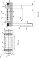
- FIG. 1A depicts a schematic top view of an example semiconductor device (e.g., a pixel) not part of the invention.
- the semiconductor device 100 includes a pinned photodiode structure 101.
- the pinned photodiode structure 101 includes a substrate 103 of a first type (e.g., a p-type material), an implant layer 105 of a second type (e.g., an n-type material), and an implant layer 107 of the first type.
- a first type e.g., a p-type material
- an implant layer 105 of a second type e.g., an n-type material
- the semiconductor device 100 further includes a first floating diffusion implant layer 109 of a second type and a second floating diffusion implant layer 111 of a second type.
- the floating diffusion layers can be floating diffusion nodes or sense nodes, for example.
- the semiconductor device 100 further includes an insulator layer 113 deposited on the substrate 103, a first transfer gate 115 (i.e., a component of an insulated gate structure), and a second transfer gate 117 (i.e., a component of another insulated gate structure), and a photo-detection region 119.
- the photo-detection region 119 is a photo-sensitive region within the semiconductor device 100 wherein incident electromagnetic radiation (e.g., ultraviolet, infrared, visible light) produces photo-generated charge-carriers.
- incident electromagnetic radiation e.g., ultraviolet, infrared, visible light
- the photo-detection region 119 includes a region of charge-carrier depletion (e.g., a region of intrinsic charge-carrier concentration).
- the insulator layer 113 can be substantially electrically insulating and substantially transparent to wavelengths of electromagnetic radiation such as electromagnetic radiation having wavelengths in the visible and/or invisible ranges (e.g., near infrared or infrared light).
- the insulator layer 113 can be composed, at least in part, of a substantially electrically insulating and transparent material (e.g., silicon dioxide or polycrystalline silicon dioxide).
- the insulator layer 113 insulates electrically the first transfer gate 115 and the second transfer gate 117 from the substrate 103.
- the substrate 103, the implant layer 105 of the second type, the implant layer 107 of the first type, the first floating diffusion implant layer 109 of the second type, and the second floating diffusion implant layer 111 of the second type can each be composed, at least in part, of a semiconductor material, such as silicon, polycrystalline silicon, germanium, indium gallium arsenide, lead sulfide, and/or indium phosphide, and can further include donor and/or acceptor dopants.
- a semiconductor material such as silicon, polycrystalline silicon, germanium, indium gallium arsenide, lead sulfide, and/or indium phosphide, and can further include donor and/or acceptor dopants.
- the implant layer 105 of the second type, the implant layer 107 of the first type, the first floating diffusion implant layer 109 of the second type, and the second floating diffusion implant layer 111 of the second type can each be the same material as the substrate 103 though, in some cases, can have a different dopant concentration or spatial distribution.
- the majority charge-carriers within the components of the first type can be holes and the majority charge-carriers within the components of the second type can can be electrons. In some cases, the majority charge-carriers within components of the first type can be electrons and the majority charge-carriers within the components of the second type can be holes. In either case, the majority charge carriers can occur intrinsically or can be introduced via acceptor (p-type) or donor (n-type) doping.
- the first transfer gate 115 and second transfer gate 117 can be composed, at least in part, of substantially transparent material (e.g., polycrystalline silicon). Voltages can be applied to the first transfer gate 115 and the second transfer gate 117. In some cases, the same voltages can be the same, while in some cases the voltages can be different. Accordingly, the first transfer gate 115 and the second transfer gate 117 can be operable to generate an electric drift field in the semiconductor device 100 (e.g., a fringe-field effect).
- substantially transparent material e.g., polycrystalline silicon
- the insulator layer 113 can have a thickness sufficient to enable the capacitive coupling between the substrate 103 and the first transfer gate 115 and second transfer gate 117 such that the voltage levels on the first and second transfer gates 115, 117, respectively, are reflected within the substrate 103 (i.e., reflected as potential distribution 120).
- an electric drift field can arise within the semiconductor device 100 (e.g., laterally within the photo-detection region 119).
- An electric drift field within the semiconductor device 100 (i.e., a potential distribution) can facilitate the conduction of photo-generated charge carries (i.e., generated within the photo-detection region 119) to either the first floating diffusion implant layer 109 or the second floating diffusion implant layer 111.
- a potential distribution as described above is illustrated in FIG. 1B .
- FIG. 1B depicts a schematic cross-sectional view and the potential distribution 120 spanning a lateral dimension of the semiconductor device depicted in FIG. 1A .
- the potential distribution 120 spanning a lateral dimension 121 of the semiconductor device 100 is depicted in a schematic plot with the lateral dimension 121 on the x-axis and potential 122 on the y -axis.
- the voltage levels on the first transfer gate 115 and the second transfer gate 117 are operable to generate a potential distribution 120 with particular characteristics intended to effect photo-generated charge-carriers.
- the potential distribution 120 depicted in FIG. 1B can conduct photo-generated charge-carriers created within the photo-detection region 119 to the second floating diffusion implant layer 111 and can inhibit charge-carriers from being conducting into the first floating diffusion implant layer 109.
- voltage levels on the first transfer gate 115 and the second transfer gate 117 can be modulated such that the semiconductor device 100 can be operable to collect modulated electromagnetic radiation (e.g., intensity modulated electromagnetic radiation) incident on the photo-detection region 119 of the semiconductor device 100.
- modulated electromagnetic radiation e.g., intensity modulated electromagnetic radiation
- Applications employing modulated electromagnetic radiation generate charge carriers with modulation characteristics of the incident modulated electromagnetic radiation. In such applications, for example, in time-of-flight applications, the charge-carriers with the modulation characteristics must necessarily be sampled at different instances in time.
- charge-carriers with the modulation characteristics are conducted through (at least partially through) the photo-detection region 119 via a potential distribution 120 (e.g., described above) and into respective first and second floating diffusion implant layers 111 at different instances in time.
- the process can be repeated over multiple instances in time, such that each first and second floating diffusion layer is occupied with sufficient charge carriers.
- the charge-carriers in each first and second floating diffusion layer can be sampled and can be used to determine useful information (e.g., distance data).
- the spatial position, concentration, spatial distribution, and purity of dopants within components of the semiconductor device 100 can significantly affect charge transport.
- dopants can be accidentally introduced into the implant layer 105 of the second type and/or the implant layer 107 of the first type via mask misalignment (during ion implantation).
- the introduced dopant can generate a potential barrier 123, as depicted in FIG. 1B , and transport efficiency between the photo-detection region 119 and the first transfer gate 115 and/or second transfer gate 117 can be degraded significantly.
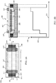
- FIG. 2A depicts a schematic top view of an example semiconductor device 200 (e.g., a demodulation pixel) operable to overcome the limitations described above, such as mask misalignment during ion implantation.
- the semiconductor device 200 includes a pinned photodiode structure 201.
- the pinned photodiode structure 201 includes a substrate 203 of a first type, an implant layer 205 of a second type and an implant layer 207 of the first type.
- the semiconductor device further includes a first auxiliary implant layer 206 of the second type and a second auxiliary implant layer 208 of the second type.
- the semiconductor device 200 further includes a first floating diffusion implant layer 209 of the second type and a second floating diffusion implant layer 211 of the second type.
- the floating diffusion implant layers 209, 211 can be floating diffusion nodes or sense nodes, for example.
- the semiconductor device 200 further includes an insulator layer 213 deposited on the substrate 203, a first transfer gate 215, and a second transfer gate 217, and a photo-detection region 219.
- Each gate i.e., the first transfer gate 215 and the second transfer gate 217) can be a component of an insulated gate structure.
- the photo-detection region 219 is a photo-sensitive region within the semiconductor device 200 wherein incident electromagnetic radiation (e.g., ultraviolet, infrared, visible light) produces photo-generated charge-carriers.
- incident electromagnetic radiation e.g., ultraviolet, infrared, visible light
- the photo-detection region 219 includes a region of charge-carrier depletion (e.g., a region of intrinsic charge-carrier concentration).
- the insulator layer 213 can be composed of a substantially electrically insulating and transparent material (e.g., silicon dioxide or polycrystalline silicon dioxide).
- the insulator layer 213 insulates electrically the first transfer gate 215 and the second transfer gate 217 from the substrate 203.
- the first transfer gate 215 and the second transfer gate 217 can be composed, at least in part, of substantially transparent material (e.g., polycrystalline silicon).
- the substrate 203, the implant layer 205 of the second type, the implant layer 207 of the first type, the first floating diffusion implant layer 209 of the second type, the second floating diffusion implant layer 211 of the second type, the first auxiliary implant layer of the second type 206, the second auxiliary implant layer 208 of the second type can each be composed, at least in part, of a semiconductor material, such as silicon, polycrystalline silicon, germanium, indium gallium arsenide, lead sulfide, and/or indium phosphide, and can further include donor and/or acceptor dopants.
- a semiconductor material such as silicon, polycrystalline silicon, germanium, indium gallium arsenide, lead sulfide, and/or indium phosphide, and can further include donor and/or acceptor dopants.
- the implant layer 205 of the second type, the implant layer 207 of the first type, the first floating diffusion implant layer 209 of the second type, the second floating diffusion implant layer 211 of the second type, the first auxiliary implant layer of the second type 206, and the second auxiliary implant layer 208 of the second type can each be the same material as the substrate 203 though, in some cases, can have a different dopant concentration or spatial distribution.
- the doping concentrations of the first auxiliary implant layer 206 of the second type and the second auxiliary implant layer 208 of the second type can be the same as the doping concentration as the implant layer 205 of the second type.
- the first auxiliary implant layer 206 of the second type and the second auxiliary implant layer 208 of the second type include a concentration gradient of dopants that varies linearly with thickness .
- the majority charge-carriers within the components of the first type can be holes and the majority charge-carriers within the components of the second type can can be electrons. In some cases, the majority charge-carriers within components of the first type can be electrons and the majority charge-carriers within the components of the second type can be holes. In either case, the majority charge carriers can occur intrinsically or can be introduced via acceptor (p-type) or donor (n-type) doping.
- Voltages can be applied to the first transfer gate 215 and the second transfer gate 217.
- the voltages can be the same, while in some cases the voltages can be different.
- the first transfer gate 215 and the second transfer gate 217 can be operable to generate an electric drift field in the semiconductor device 200 (e.g., a fringe-field effect).
- the insulator layer 213 can have a thickness sufficient to enable the capacitive coupling between the substrate 203 and the first transfer gate 215 and second transfer gate 217 such that the voltage levels on the first and second transfer gates 215, 217, respectively, are reflected within the substrate 203 (i.e., reflected as potential distribution 220).
- an electric drift field can arise within the semiconductor device 200 (e.g., laterally within the photo-detection region 219).
- An electric drift field within 9794712-1 the semiconductor device 200 i.e., a potential distribution
- a dopant concentration gradient through the first auxiliary implant layer 206 and second auxiliary implant layer 208 can inhibit the formation of potential barriers caused by mask misalignment during ion implantation. Such a potential distribution as described above is illustrated in FIG. 2B .
- FIG. 2B depicts a schematic cross-sectional view and a potential distribution 220 spanning a lateral dimension of the semiconductor device 200 depicted in FIG. 2A .
- the potential distribution 220 spanning a lateral dimension 221 of the semiconductor device 200 is depicted in a schematic plot with the lateral dimension 221 on the x-axis and potential 222 on the y -axis.
- the voltage levels on the first transfer gate 215 and the second transfer gate 217 are operable to generate a potential distribution 220 with particular characteristics.
- the potential distribution 220 depicted in FIG. 2B can conduct charges generated within the photo-detection region 219 to the second floating diffusion implant layer 211 via the second floating diffusion implant layer 211 and can inhibit charge carriers from being conducted into the first floating diffusion implant layer 209.
- the implant layer 207 of the second type can extend under the first transfer gate 215 and/or the second transfer gate 217.
- the first auxiliary implant layer 206 of the second type can extend under the first transfer gate 215.
- the second auxiliary implant layer 208 of the second type can extend under the second transfer gate 217.
- the first auxiliary implant layer 206 of the second type can abut the first floating diffusion layer 209.
- the second auxiliary implant layer 208 of the second type can abut the second floating diffusion layer 211.
- Other configuration are within the scope of this disclosure; for example, at least one additional transfer gate, at least one additional auxiliary implant layer, and at least one additional floating diffusion layer can be includes in some implementations.
- voltage levels on the first transfer gate 215 and the second transfer gate 217 can be modulated such that the semiconductor device 200 can be operable to collect modulated electromagnetic radiation (e.g., intensity modulated electromagnetic radiation) incident on the photo-detection region 219 of the semiconductor device 200.
- modulated electromagnetic radiation e.g., intensity modulated electromagnetic radiation
- Applications employing modulated electromagnetic radiation generate charge carriers with modulation characteristics of the incident modulated electromagnetic radiation. In such applications, for example, in time-of-flight applications, the charge-carriers with the modulation characteristics must necessarily be sampled at different instances in time.
- charge-carriers with the modulation characteristics are conducted through (at least partially through) the photo-detection region 219 via a potential distribution 220 (e.g., described above) and into respective first and second floating diffusion implant layers 209, 211 (via the first auxiliary implant layer 206 of the second type and a second auxiliary implant layer 208 of the second type) at different instances in time.
- the process can be repeated over multiple instances in time, such that each first and second floating diffusion layer 209, 211 is occupied with sufficient charge carriers.
- the charge-carriers in each first and second floating diffusion layer 209, 211 can be sampled and can be used to determine useful information (e.g., distance data).
- FIG 3 depicts a schematic top view of another example semiconductor device 300 (e.g., a demodulation pixel) operable to overcome the limitations described above, such as mask misalignment during ion implantation.
- the semiconductor device 300 includes a pinned photodiode structure 301.
- the pinned photodiode structure 301 includes a substrate 303 of a first type, an implant layer 305 of a second type and an implant layer 307 of the first type.
- the semiconductor device further includes a first auxiliary implant layer 306 of the second type, a second auxiliary implant layer 308 of the second type, and a dump auxiliary implant layer 310 of a second type.
- the semiconductor device 300 further includes a first floating diffusion implant layer 309 of the second type, a second floating diffusion implant layer 311 of the second type, and a dump floating diffusion implant layer 312 of the second type.
- the floating diffusion implant layers can be floating diffusion nodes or sense nodes, for example.
- the semiconductor device 300 further includes an insulator layer 313 deposited on the substrate 303, a first transfer gate 315, a second transfer gate 317, a dump gate 318, and a photo-detection region 319.
- Each gate i.e., the first transfer gate 315, the second transfer gate 317, and the dump gate 318) can be a component of an insulated gate structure.
- the photo-detection region 319 is a photo-sensitive region within the semiconductor device 300 wherein incident electromagnetic radiation (e.g., ultraviolet, infrared, visible light) produces photo-generated charge-carriers.
- incident electromagnetic radiation e.g., ultraviolet, infrared, visible light
- the photo-detection region 319 includes a region of charge-carrier depletion (e.g., a region of intrinsic charge-carrier concentration).
- the insulator layer 313 can be composed of a substantially electrically insulating and transparent material (e.g., silicon dioxide or polycrystalline silicon dioxide).
- the insulator layer 313 insulates electrically the first transfer gate 315 and the second transfer gate 317 from the substrate 303.
- the first transfer gate 315, the second transfer gate 317, and the dump gate 318 can be composed, at least in part, of substantially transparent material (e.g., polycrystalline silicon).
- the substrate 303, the implant layer 305 of the second type, the implant layer 307 of the first type, the first floating diffusion implant layer 309 of the second type, the second floating diffusion implant layer 311 of the second type, the first auxiliary implant layer of the second type 306, the second auxiliary implant layer 308 of the second type, the dump auxiliary implant layer 310 of the second type, and the dump floating diffusion implant layer 312 of the second type can each be composed, at least in part, of a semiconductor material, such as silicon, polycrystalline silicon, germanium, indium gallium arsenide, lead sulfide, and/or indium phosphide, and can further include donor and/or acceptor dopants.
- a semiconductor material such as silicon, polycrystalline silicon, germanium, indium gallium arsenide, lead sulfide, and/or indium phosphide, and can further include donor and/or acceptor dopants.
- the implant layer 305 of the second type, the implant layer 307 of the first type, the first floating diffusion implant layer 309 of the second type, the second floating diffusion implant layer 311 of the second type, the first auxiliary implant layer of the second type 306, the second auxiliary implant layer 308 of the second type, the dump auxiliary implant layer 310 of the second type, and the dump floating diffusion implant layer 312 of the second type can each be the same material as the substrate 303 though, in some cases, can have a different dopant concentration or spatial dopant distribution.
- the doping concentrations of the first auxiliary implant layer 306 of the second type, the second auxiliary implant layer 308 of the second type, and the dump auxiliary implant layer 310 of the second type can be the same as the doping concentration as the implant layer 305 of the second type.
- the first auxiliary implant layer 306 of the second type, the second auxiliary implant layer 308 of the second type, and the dump auxiliary implant layer 310 of the second type could include a concentration gradient of dopants (e.g., the dopant concertation could vary linearly with thickness or some other dimension).
- the majority charge-carriers within the components of the first type can be holes and the majority charge-carriers within the components of the second type can can be electrons. In some cases, the majority charge-carriers within components of the first type can be electrons and the majority charge-carriers within the components of the second type can be holes. In either case, the majority charge carriers can occur intrinsically or can be introduced via acceptor (p-type) or donor (n-type) doping.
- Voltages can be applied to the first transfer gate 315, the second transfer gate 317, and the dump gate 318.
- the voltages can be the same, while in some cases the voltages can be different.
- the first transfer gate 315, the second transfer gate 317, and the dump gate 318 can be operable to generate an electric drift field in the semiconductor device 300 (e.g., a fringe-field effect).
- the insulator layer 313 can have a thickness sufficient to enable the capacitive coupling between the substrate 303 and the first transfer gate 315, the second transfer gate 317, and the dump gate 318 such that the voltage levels on the first and second transfer gates 315, 317, respectively, and the dump gate 318 are reflected within the substrate 303.
- an electric drift field can arise within the semiconductor device 300 (e.g., laterally within the photo-detection region 319).
- An electric drift field within the semiconductor device 300 i.e., a potential distribution
- Charge-carriers associated with background electromagnetic radiation for example, can be conducted to the dump floating diffusion implant layer 312.
- a dopant concentration gradient through the first auxiliary implant layer 306, the second auxiliary implant layer 308, and the dump auxiliary layer 310 can inhibit the formation of potential barriers caused by mask misalignment during ion implantation.
- the implant layer 307 of the second type can extend under the first transfer gate 315 and/or the second transfer gate 317 and/or the dump gate 318.
- the first auxiliary implant layer 306 of the second type can extend under the first transfer gate 315.
- the second auxiliary implant layer 308 of the second type can extend under the second transfer gate 317.
- the dump auxiliary implant layer 310 can extend under the dump gate 318.
- the first auxiliary implant layer 306 of the second type can abut the first floating diffusion layer 309.
- the second auxiliary implant layer 308 of the second type can abut the second floating diffusion layer 311.
- the dump auxiliary layer 310 can abut the dump floating diffusion implant layer 312.
- Other configurations are within the scope of this disclosure; for example, at least one additional transfer gate, at least one additional auxiliary implant layer, and at least one additional floating diffusion layer can be included in some implementations.
- voltage levels on the first transfer gate 315, the second transfer gate 317, and the dump gate 318 can be modulated such that the semiconductor device 300 can be operable to collect modulated electromagnetic radiation (e.g., intensity modulated electromagnetic radiation) incident on the photo-detection region 319 of the semiconductor device 300.
- modulated electromagnetic radiation e.g., intensity modulated electromagnetic radiation
- Applications employing modulated electromagnetic radiation generate charge carriers with modulation characteristics of the incident modulated electromagnetic radiation. In such applications, for example, in time-of-flight applications, the charge-carriers with the modulation characteristics must necessarily be sampled at different instances in time.
- charge-carriers with the modulation characteristics can be conducted through (at least partially through) the photo-detection region 319 into respective first and second floating diffusion implant layers 309, 311 (via the first auxiliary implant layer 306 of the second type and a second auxiliary implant layer 308 of the second type) at different instances in time.
- Charge-carriers without modulation characteristics e.g., charge-carriers associated with background electromagnetic radiation
- can be electromagnetic radiation that is not modulated can be conducted to through (at least partially though) the photo-detection region 319 into the dump floating diffusion implant layer 312 via the dump auxiliary implant layer 310.
- each first and second floating diffusion layer 309, 311 are occupied with sufficient charge carriers and the charge-carriers without modulation characteristics (e.g., associated with background electromagnetic radiation) are essentially eliminated. Accordingly, the charge-carriers in each first and second floating diffusion layer 309, 311 can be sampled and can be used to determine useful information (e.g., distance data) without being compromised by charge-carries without modulation characteristics, such as background electromagnetic radiation.
Landscapes
- Solid State Image Pick-Up Elements (AREA)
- Light Receiving Elements (AREA)
Claims (13)
- Halbleitervorrichtung (100, 200, 300), welche bedienbar ist, um eine einfallende modulierte elektromagnetische Strahlung zu demodulieren, wobei die Halbleitervorrichtung (100, 200, 300) Folgendes umfasst:eine verstiftete Photodiodenstruktur (101, 201, 301), welche ein Substrat (103, 203, 303) einer ersten Art einschließt;eine Implantatschicht (105, 205, 305) einer zweiten Art, welche innerhalb des Substrates (103, 203, 303) angeordnet ist;eine erste zusätzliche Implantatschicht (206, 306) der zweiten Art, welche innerhalb des Substrates (103, 203, 303) und angrenzend an die Implantatschicht (105, 205, 305) der zweiten Art angeordnet ist;eine erste zusätzliche Implantatschicht (208, 308) der zweiten Art, welche innerhalb des Substrates (103, 203, 303) und angrenzend an die Implantatschicht der zweiten Art angeordnet ist;eine Implantatschicht (107, 207, 307) der ersten Art, welche innerhalb der Implantatschicht der zweiten Art angeordnet ist und sich in die erste zusätzliche Implantatschicht der zweiten Art und die zweite zusätzliche Implantatschicht der zweiten Art erstreckt;einen Isolator (113, 213, 313), welcher an einer Oberfläche des Substrates (103, 203, 303) angeordnet ist;einen Lichterfassungsbereich (119, 219, 319);ein erstes Transfergate (115, 215, 315) und ein zweites Transfergate (117, 217, 317), welche an einer Oberfläche des Isolators angeordnet sind, wobei das erste Transfergate (115, 215, 315) und das zweite Transfergate (117, 217, 317) bedienbar sind, um ein Feld innerhalb des Substrates der ersten Art zu erzeugen; undeine erste schwebende Diffusionsimplantatschicht (109, 209, 309) einer zweiten Art und eine zweite schwebende Diffusionsimplantatschicht (111, 211, 311) einer zweiten Art, welche innerhalb des Substrates der ersten Art angeordnet sind,wobei die erste und die zweite zusätzliche Implantatschicht (206, 306, 208, 308) der zweiten Art jeweils einen Konzentrationsgradienten an Dotierungsmitteln aufweist, welcher linear entsprechend der Dicke variiert.
- Halbleitervorrichtung (100, 200, 300) nach Anspruch 1, wobei die Halbleitervorrichtung (100, 200, 300) bedienbar ist, um Ladungsträger der zweiten Art aus modulierter elektromagnetischer Strahlung zu erzeugen, welche auf den Lichterfassungsbereich (119, 219, 319) einfällt, wobei die erzeugten Ladungsträger Modulationsmerkmale der einfallenden modulierten elektromagnetischen Strahlung aufweisen.
- Halbleitervorrichtung (100, 200, 300) nach Anspruch 2, wobei das erste Transfergate (115, 215, 315) und das zweite Transfergate (117, 217, 317) bedienbar sind, um abwechselnd Ladungsträger zu der ersten schwebenden Diffusionsimplantatschicht (109, 209, 309) zu leiten und zu der zweiten schwebenden Diffusionsimplantatschicht (111, 211, 311) zu leiten.
- Halbleitervorrichtung (100, 200, 300) nach Anspruch 1, wobei sich die erste zusätzliche Implantatschicht der zweiten Art (206, 306) unter dem ersten Transfergate (115, 215, 315) erstreckt und die zweite zusätzliche Implantatschicht der zweiten Art sich unter dem zweiten Transfergate (117, 217, 317) erstreckt.
- Halbleitervorrichtung (100, 200, 300) nach Anspruch 1, wobei die erste zusätzliche Implantatschicht (206, 306) der zweiten Art an die erste schwebende Diffusionsimplantatschicht (109, 209, 309) der zweiten Art anstößt, und wobei optionsweise die zweite zusätzliche Implantatschicht (208, 308) der zweiten Art an die zweite schwebende Diffusionsimplantatschicht (111, 211, 311) der zweiten Art anstößt.
- Halbleitervorrichtung (100, 200, 300) nach Anspruch 1, wobei die erste und die zweite zusätzliche Implantatschicht (206, 306, 208, 308) der zweiten Art an die Implantatschicht (105, 205, 305) der zweiten Art angrenzen.
- Halbleitervorrichtung (100, 200, 300) nach Anspruch 1, ferner einschließend mindestens ein zusätzliches Transfergate, welches an einer Oberfläche des Isolators (113, 213, 313) angeordnet ist, wobei das mindestens eine zusätzliche Transfergate bedienbar ist, um ein Feld innerhalb des Substrates (103, 203, 303) der ersten Art zu erzeugen.
- Halbleitervorrichtung (100, 200, 300) nach Anspruch 7, ferner einschließend mindestens eine weitere schwebende Diffusionsimplantatschicht der zweiten Art, welche innerhalb des Substrates (103, 203, 303) der ersten Art angeordnet ist, und mindestens eine weitere zusätzliche Implantatschicht der zweiten Art, welche angrenzend an die Implantatschicht (105, 205, 305) der zweiten Art angeordnet ist.
- Halbleitervorrichtung (100, 200, 300) nach Anspruch 8, wobei die Halbleitervorrichtung (100, 200, 300) bedienbar ist, um Ladungsträger der zweiten Art aus modulierter elektromagnetischer Strahlung zu erzeugen, welche auf den Lichterfassungsbereich (119, 219, 319) einfällt, wobei die erzeugten Ladungsträger Modulationsmerkmale der einfallenden modulierten elektromagnetischen Strahlung aufweisen, und wobei optionsweise das erste Transfergate (115, 215, 315), das zweite Transfergate (117, 217, 317) und das mindestens eine weitere Transfergate bedienbar sind, um abwechselnd Ladungsträger zu der ersten schwebenden Diffusionsimplantatschicht (109, 209, 309), zu der zweiten schwebenden Diffusionsimplantatschicht (111) und zu der mindestens einen weiteren schwebenden Diffusionsimplantatschicht zu leiten.
- Halbleitervorrichtung (100, 200, 300) nach Anspruch 1, wobei die Halbleitervorrichtung (100, 200, 300) bedienbar ist, um Ladungsträger der zweiten Art aus elektromagnetischer Strahlung zu erzeugen, welche auf den Lichterfassungsbereich (119, 219, 319) einfällt.
- Halbleitervorrichtung (100, 200, 300) nach Anspruch 10, ferner einschließend mindestens ein Abwurfgate (318), welches an einer Oberfläche des Isolators (113, 213, 313) angeordnet ist, wobei das mindestens eine Abwurfgate (318) bedienbar ist, um ein Feld innerhalb des Substrates (103, 203, 303) der ersten Art zu erzeugen; mindestens eine schwebende Abwurf-Diffusionsimplantatschicht (312) der zweiten Art, welche innerhalb des Substrates (103, 203, 303) der ersten Art angeordnet ist; und mindestens eine weitere zusätzliche Abwurf-Implantatschicht (310) der zweiten Art, welche angrenzend an die Implantatschicht (105, 205, 305) der zweiten Art angeordnet ist.
- Halbleitervorrichtung (100, 200, 300) nach Anspruch 11, wobei das erste Transfergate (115, 215, 315), das zweite Transfergate (117, 217, 317) und das Abwurfgate (318) bedienbar sind, um Ladungsträger zu der mindestens einen schwebenden Abwurf-Diffusionsschicht (312) zu leiten, und wobei optionsweise das erste Transfergate (115, 215, 315), das zweite Transfergate (117, 217, 317) und das Abwurfgate (318) bedienbar sind, um abwechselnd Ladungsträger zu der ersten schwebenden Diffusionsimplantatschicht (109, 209, 309), zu der zweiten schwebenden Diffusionsimplantatschicht (111, 211, 311) und zu der schwebenden Abwurf-Diffusionsimplantatschicht (312) zu leiten.
- Halbleitervorrichtung (100, 200, 300) nach Anspruch 11, wobei sich die erste zusätzliche Implantatschicht (206, 306) der zweiten Art unter das erste Transfergate (115, 215, 315) erstreckt, sich die zweite zusätzliche Implantatschicht (208, 308) der zweiten Art unter das zweite Transfergate (117, 317) erstreckt, die zusätzliche Abwurf-Implantatschicht (310) der zweiten Art sich unter das Abwurfgate (318) erstreckt und die zusätzliche Abwurf-Implantatschicht (310) einen Konzentrationsgradienten an Dotierungsmitteln aufweist, welcher linear entsprechend der Dicke variiert.
Applications Claiming Priority (2)
| Application Number | Priority Date | Filing Date | Title |
|---|---|---|---|
| US201662279076P | 2016-01-15 | 2016-01-15 | |
| PCT/SG2017/050019 WO2017123159A1 (en) | 2016-01-15 | 2017-01-16 | Semiconductor devices comprising a pinned photodiode structure |
Publications (3)
| Publication Number | Publication Date |
|---|---|
| EP3403284A1 EP3403284A1 (de) | 2018-11-21 |
| EP3403284A4 EP3403284A4 (de) | 2019-01-16 |
| EP3403284B1 true EP3403284B1 (de) | 2021-03-03 |
Family
ID=59311985
Family Applications (1)
| Application Number | Title | Priority Date | Filing Date |
|---|---|---|---|
| EP17738734.7A Active EP3403284B1 (de) | 2016-01-15 | 2017-01-16 | Halbleiterbauelemente mit einer verstifteten photodiodenstruktur |
Country Status (5)
| Country | Link |
|---|---|
| US (1) | US10861889B2 (de) |
| EP (1) | EP3403284B1 (de) |
| CN (1) | CN108701729B (de) |
| TW (1) | TWI731026B (de) |
| WO (1) | WO2017123159A1 (de) |
Families Citing this family (1)
| Publication number | Priority date | Publication date | Assignee | Title |
|---|---|---|---|---|
| WO2020234649A1 (en) * | 2019-05-21 | 2020-11-26 | Sony Semiconductor Solutions Corporation | Capacitance matched metal wirings in dual conversion gain pixels |
Family Cites Families (20)
| Publication number | Priority date | Publication date | Assignee | Title |
|---|---|---|---|---|
| US5903021A (en) * | 1997-01-17 | 1999-05-11 | Eastman Kodak Company | Partially pinned photodiode for solid state image sensors |
| US7087944B2 (en) * | 2003-01-16 | 2006-08-08 | Micron Technology, Inc. | Image sensor having a charge storage region provided within an implant region |
| US6900484B2 (en) * | 2003-07-30 | 2005-05-31 | Micron Technology, Inc. | Angled pinned photodiode for high quantum efficiency |
| KR100535926B1 (ko) * | 2003-09-22 | 2005-12-09 | 동부아남반도체 주식회사 | 씨모스 이미지 센서 제조 방법 |
| US7635880B2 (en) * | 2004-12-30 | 2009-12-22 | Ess Technology, Inc. | Method and apparatus for proximate CMOS pixels |
| ATE390715T1 (de) | 2005-10-19 | 2008-04-15 | Suisse Electronique Microtech | Einrichtung und verfahren zur demodulation von modulierten elektromagnetischen wellenfeldern |
| EP1777811B1 (de) | 2005-10-19 | 2018-10-03 | Heptagon Micro Optics Pte. Ltd. | Verfahren und Vorrichtung zum demodulieren eines modulierten optischen Signals |
| US7586077B2 (en) | 2007-07-18 | 2009-09-08 | Mesa Imaging Ag | Reference pixel array with varying sensitivities for time of flight (TOF) sensor |
| US20090224139A1 (en) * | 2008-03-04 | 2009-09-10 | Mesa Imaging Ag | Drift Field Demodulation Pixel with Pinned Photo Diode |
| JP4788742B2 (ja) * | 2008-06-27 | 2011-10-05 | ソニー株式会社 | 固体撮像装置及び電子機器 |
| EP2316221A1 (de) | 2008-08-28 | 2011-05-04 | MESA Imaging AG | Demodulationspixel mit verketteten ladespeicherorten und betriebsverfahren dafür |
| US9117712B1 (en) | 2009-07-24 | 2015-08-25 | Mesa Imaging Ag | Demodulation pixel with backside illumination and charge barrier |
| GB2477083A (en) | 2010-01-13 | 2011-07-27 | Cmosis Nv | Pixel structure with multiple transfer gates to improve dynamic range |
| ITMI20100091A1 (it) * | 2010-01-26 | 2011-07-27 | Fond Bruno Kessler | Demodulatore elettro-ottico basato su fotodiodo sepolto |
| KR20110093212A (ko) * | 2010-02-12 | 2011-08-18 | 삼성전자주식회사 | 이미지 센서의 픽셀 및 픽셀 동작 방법 |
| FR2986906B1 (fr) * | 2012-02-15 | 2015-06-19 | New Imaging Technologies Sas | Structure de pixel actif a transfert de charge ameliore |
| EP2822270A1 (de) * | 2012-02-27 | 2015-01-07 | Sony Corporation | Bildaufzeichnungselement und elektronische vorrichtung damit |
| KR102252647B1 (ko) * | 2014-07-11 | 2021-05-17 | 삼성전자주식회사 | 이미지 센서의 픽셀 및 이미지 센서 |
| CN104362198B (zh) * | 2014-11-03 | 2016-07-06 | 长沙理工大学 | 透明电极栅控横向pin蓝紫光探测器及其制备方法 |
| FR3046495B1 (fr) * | 2015-12-30 | 2018-02-16 | Stmicroelectronics (Crolles 2) Sas | Pixel de detection de temps de vol |
-
2017
- 2017-01-13 TW TW106101281A patent/TWI731026B/zh active
- 2017-01-16 WO PCT/SG2017/050019 patent/WO2017123159A1/en not_active Ceased
- 2017-01-16 EP EP17738734.7A patent/EP3403284B1/de active Active
- 2017-01-16 US US16/069,986 patent/US10861889B2/en active Active
- 2017-01-16 CN CN201780011654.6A patent/CN108701729B/zh active Active
Non-Patent Citations (1)
| Title |
|---|
| None * |
Also Published As
| Publication number | Publication date |
|---|---|
| WO2017123159A1 (en) | 2017-07-20 |
| US10861889B2 (en) | 2020-12-08 |
| TW201733147A (zh) | 2017-09-16 |
| EP3403284A1 (de) | 2018-11-21 |
| TWI731026B (zh) | 2021-06-21 |
| US20190027516A1 (en) | 2019-01-24 |
| EP3403284A4 (de) | 2019-01-16 |
| CN108701729A (zh) | 2018-10-23 |
| CN108701729B (zh) | 2022-02-25 |
Similar Documents
| Publication | Publication Date | Title |
|---|---|---|
| US11791359B2 (en) | Light detecting element and method of manufacturing same | |
| TWI734709B (zh) | 解調變像素裝置、像素裝置陣列及包含其之光電裝置 | |
| KR100298178B1 (ko) | 이미지센서의포토다이오드 | |
| US7205627B2 (en) | Image sensor cells | |
| US8890219B2 (en) | UTBB CMOS imager having a diode junction in a photosensitive area thereof | |
| JP2019134167A (ja) | 多数電流によって補助される放射線検出器デバイス | |
| US10692921B2 (en) | Method of manufacturing an imager and imager device | |
| KR102682692B1 (ko) | 애벌란치 포토다이오드 어레이 | |
| US10978606B2 (en) | Avalanche diode and method of manufacturing an avalanche diode | |
| US7205591B2 (en) | Pixel sensor cell having reduced pinning layer barrier potential and method thereof | |
| KR20180028752A (ko) | 광 검출 장치 | |
| KR20080011468A (ko) | 고 양자 효율을 위한 각도를 가지는 핀드 포토다이오드 및그 형성 방법 | |
| US8994138B2 (en) | Hardened photodiode image sensor | |
| US20210175264A1 (en) | Photoelectric conversion element and solid-state imaging device | |
| GB2106314A (en) | Infra-red radiation imaging devices | |
| CN115050766A (zh) | 图像传感器及其形成方法 | |
| US20240241229A1 (en) | SINGLE PHOTON DETECTOR, ELECTRONIC DEVICE, AND LiDAR DEVICE | |
| US10861889B2 (en) | Semiconductor devices | |
| US8513753B1 (en) | Photodiode having a buried well region | |
| US20250351595A1 (en) | Semiconductor image sensor device | |
| US12113141B2 (en) | Optical-sensing apparatus | |
| US20240186432A1 (en) | Method for manufacturing deep-junction low-gain avalanche detectors and associated semiconductor substrates | |
| KR100298201B1 (ko) | 이미지센서의 저전압 포토다이오드 형성방법 | |
| KR100718775B1 (ko) | 이미지 센서 및 그 제조방법 |
Legal Events
| Date | Code | Title | Description |
|---|---|---|---|
| STAA | Information on the status of an ep patent application or granted ep patent |
Free format text: STATUS: THE INTERNATIONAL PUBLICATION HAS BEEN MADE |
|
| PUAI | Public reference made under article 153(3) epc to a published international application that has entered the european phase |
Free format text: ORIGINAL CODE: 0009012 |
|
| STAA | Information on the status of an ep patent application or granted ep patent |
Free format text: STATUS: REQUEST FOR EXAMINATION WAS MADE |
|
| 17P | Request for examination filed |
Effective date: 20180814 |
|
| AK | Designated contracting states |
Kind code of ref document: A1 Designated state(s): AL AT BE BG CH CY CZ DE DK EE ES FI FR GB GR HR HU IE IS IT LI LT LU LV MC MK MT NL NO PL PT RO RS SE SI SK SM TR |
|
| AX | Request for extension of the european patent |
Extension state: BA ME |
|
| A4 | Supplementary search report drawn up and despatched |
Effective date: 20181219 |
|
| RIC1 | Information provided on ipc code assigned before grant |
Ipc: H01L 31/111 20060101ALI20181213BHEP Ipc: H01L 31/0352 20060101AFI20181213BHEP Ipc: H01L 21/265 20060101ALI20181213BHEP Ipc: H01L 31/11 20060101ALI20181213BHEP Ipc: H01L 21/329 20060101ALI20181213BHEP Ipc: H01L 21/33 20060101ALI20181213BHEP Ipc: H01L 27/146 20060101ALI20181213BHEP |
|
| DAV | Request for validation of the european patent (deleted) | ||
| DAX | Request for extension of the european patent (deleted) | ||
| STAA | Information on the status of an ep patent application or granted ep patent |
Free format text: STATUS: EXAMINATION IS IN PROGRESS |
|
| 17Q | First examination report despatched |
Effective date: 20200409 |
|
| GRAP | Despatch of communication of intention to grant a patent |
Free format text: ORIGINAL CODE: EPIDOSNIGR1 |
|
| STAA | Information on the status of an ep patent application or granted ep patent |
Free format text: STATUS: GRANT OF PATENT IS INTENDED |
|
| INTG | Intention to grant announced |
Effective date: 20200715 |
|
| GRAS | Grant fee paid |
Free format text: ORIGINAL CODE: EPIDOSNIGR3 |
|
| GRAA | (expected) grant |
Free format text: ORIGINAL CODE: 0009210 |
|
| STAA | Information on the status of an ep patent application or granted ep patent |
Free format text: STATUS: THE PATENT HAS BEEN GRANTED |
|
| AK | Designated contracting states |
Kind code of ref document: B1 Designated state(s): AL AT BE BG CH CY CZ DE DK EE ES FI FR GB GR HR HU IE IS IT LI LT LU LV MC MK MT NL NO PL PT RO RS SE SI SK SM TR |
|
| REG | Reference to a national code |
Ref country code: GB Ref legal event code: FG4D |
|
| REG | Reference to a national code |
Ref country code: AT Ref legal event code: REF Ref document number: 1368168 Country of ref document: AT Kind code of ref document: T Effective date: 20210315 Ref country code: CH Ref legal event code: EP |
|
| REG | Reference to a national code |
Ref country code: DE Ref legal event code: R096 Ref document number: 602017033824 Country of ref document: DE |
|
| REG | Reference to a national code |
Ref country code: IE Ref legal event code: FG4D |
|
| REG | Reference to a national code |
Ref country code: LT Ref legal event code: MG9D |
|
| PG25 | Lapsed in a contracting state [announced via postgrant information from national office to epo] |
Ref country code: LT Free format text: LAPSE BECAUSE OF FAILURE TO SUBMIT A TRANSLATION OF THE DESCRIPTION OR TO PAY THE FEE WITHIN THE PRESCRIBED TIME-LIMIT Effective date: 20210303 Ref country code: BG Free format text: LAPSE BECAUSE OF FAILURE TO SUBMIT A TRANSLATION OF THE DESCRIPTION OR TO PAY THE FEE WITHIN THE PRESCRIBED TIME-LIMIT Effective date: 20210603 Ref country code: GR Free format text: LAPSE BECAUSE OF FAILURE TO SUBMIT A TRANSLATION OF THE DESCRIPTION OR TO PAY THE FEE WITHIN THE PRESCRIBED TIME-LIMIT Effective date: 20210604 Ref country code: FI Free format text: LAPSE BECAUSE OF FAILURE TO SUBMIT A TRANSLATION OF THE DESCRIPTION OR TO PAY THE FEE WITHIN THE PRESCRIBED TIME-LIMIT Effective date: 20210303 Ref country code: HR Free format text: LAPSE BECAUSE OF FAILURE TO SUBMIT A TRANSLATION OF THE DESCRIPTION OR TO PAY THE FEE WITHIN THE PRESCRIBED TIME-LIMIT Effective date: 20210303 Ref country code: NO Free format text: LAPSE BECAUSE OF FAILURE TO SUBMIT A TRANSLATION OF THE DESCRIPTION OR TO PAY THE FEE WITHIN THE PRESCRIBED TIME-LIMIT Effective date: 20210603 |
|
| REG | Reference to a national code |
Ref country code: NL Ref legal event code: MP Effective date: 20210303 |
|
| REG | Reference to a national code |
Ref country code: AT Ref legal event code: MK05 Ref document number: 1368168 Country of ref document: AT Kind code of ref document: T Effective date: 20210303 |
|
| PG25 | Lapsed in a contracting state [announced via postgrant information from national office to epo] |
Ref country code: SE Free format text: LAPSE BECAUSE OF FAILURE TO SUBMIT A TRANSLATION OF THE DESCRIPTION OR TO PAY THE FEE WITHIN THE PRESCRIBED TIME-LIMIT Effective date: 20210303 Ref country code: RS Free format text: LAPSE BECAUSE OF FAILURE TO SUBMIT A TRANSLATION OF THE DESCRIPTION OR TO PAY THE FEE WITHIN THE PRESCRIBED TIME-LIMIT Effective date: 20210303 Ref country code: PL Free format text: LAPSE BECAUSE OF FAILURE TO SUBMIT A TRANSLATION OF THE DESCRIPTION OR TO PAY THE FEE WITHIN THE PRESCRIBED TIME-LIMIT Effective date: 20210303 Ref country code: LV Free format text: LAPSE BECAUSE OF FAILURE TO SUBMIT A TRANSLATION OF THE DESCRIPTION OR TO PAY THE FEE WITHIN THE PRESCRIBED TIME-LIMIT Effective date: 20210303 |
|
| PG25 | Lapsed in a contracting state [announced via postgrant information from national office to epo] |
Ref country code: NL Free format text: LAPSE BECAUSE OF FAILURE TO SUBMIT A TRANSLATION OF THE DESCRIPTION OR TO PAY THE FEE WITHIN THE PRESCRIBED TIME-LIMIT Effective date: 20210303 |
|
| PG25 | Lapsed in a contracting state [announced via postgrant information from national office to epo] |
Ref country code: SM Free format text: LAPSE BECAUSE OF FAILURE TO SUBMIT A TRANSLATION OF THE DESCRIPTION OR TO PAY THE FEE WITHIN THE PRESCRIBED TIME-LIMIT Effective date: 20210303 Ref country code: AT Free format text: LAPSE BECAUSE OF FAILURE TO SUBMIT A TRANSLATION OF THE DESCRIPTION OR TO PAY THE FEE WITHIN THE PRESCRIBED TIME-LIMIT Effective date: 20210303 Ref country code: EE Free format text: LAPSE BECAUSE OF FAILURE TO SUBMIT A TRANSLATION OF THE DESCRIPTION OR TO PAY THE FEE WITHIN THE PRESCRIBED TIME-LIMIT Effective date: 20210303 Ref country code: CZ Free format text: LAPSE BECAUSE OF FAILURE TO SUBMIT A TRANSLATION OF THE DESCRIPTION OR TO PAY THE FEE WITHIN THE PRESCRIBED TIME-LIMIT Effective date: 20210303 |
|
| PG25 | Lapsed in a contracting state [announced via postgrant information from national office to epo] |
Ref country code: PT Free format text: LAPSE BECAUSE OF FAILURE TO SUBMIT A TRANSLATION OF THE DESCRIPTION OR TO PAY THE FEE WITHIN THE PRESCRIBED TIME-LIMIT Effective date: 20210705 Ref country code: RO Free format text: LAPSE BECAUSE OF FAILURE TO SUBMIT A TRANSLATION OF THE DESCRIPTION OR TO PAY THE FEE WITHIN THE PRESCRIBED TIME-LIMIT Effective date: 20210303 Ref country code: SK Free format text: LAPSE BECAUSE OF FAILURE TO SUBMIT A TRANSLATION OF THE DESCRIPTION OR TO PAY THE FEE WITHIN THE PRESCRIBED TIME-LIMIT Effective date: 20210303 Ref country code: IS Free format text: LAPSE BECAUSE OF FAILURE TO SUBMIT A TRANSLATION OF THE DESCRIPTION OR TO PAY THE FEE WITHIN THE PRESCRIBED TIME-LIMIT Effective date: 20210703 |
|
| REG | Reference to a national code |
Ref country code: DE Ref legal event code: R097 Ref document number: 602017033824 Country of ref document: DE |
|
| PLBE | No opposition filed within time limit |
Free format text: ORIGINAL CODE: 0009261 |
|
| STAA | Information on the status of an ep patent application or granted ep patent |
Free format text: STATUS: NO OPPOSITION FILED WITHIN TIME LIMIT |
|
| PG25 | Lapsed in a contracting state [announced via postgrant information from national office to epo] |
Ref country code: ES Free format text: LAPSE BECAUSE OF FAILURE TO SUBMIT A TRANSLATION OF THE DESCRIPTION OR TO PAY THE FEE WITHIN THE PRESCRIBED TIME-LIMIT Effective date: 20210303 Ref country code: DK Free format text: LAPSE BECAUSE OF FAILURE TO SUBMIT A TRANSLATION OF THE DESCRIPTION OR TO PAY THE FEE WITHIN THE PRESCRIBED TIME-LIMIT Effective date: 20210303 Ref country code: AL Free format text: LAPSE BECAUSE OF FAILURE TO SUBMIT A TRANSLATION OF THE DESCRIPTION OR TO PAY THE FEE WITHIN THE PRESCRIBED TIME-LIMIT Effective date: 20210303 |
|
| 26N | No opposition filed |
Effective date: 20211206 |
|
| PG25 | Lapsed in a contracting state [announced via postgrant information from national office to epo] |
Ref country code: SI Free format text: LAPSE BECAUSE OF FAILURE TO SUBMIT A TRANSLATION OF THE DESCRIPTION OR TO PAY THE FEE WITHIN THE PRESCRIBED TIME-LIMIT Effective date: 20210303 |
|
| PG25 | Lapsed in a contracting state [announced via postgrant information from national office to epo] |
Ref country code: IT Free format text: LAPSE BECAUSE OF FAILURE TO SUBMIT A TRANSLATION OF THE DESCRIPTION OR TO PAY THE FEE WITHIN THE PRESCRIBED TIME-LIMIT Effective date: 20210303 |
|
| PG25 | Lapsed in a contracting state [announced via postgrant information from national office to epo] |
Ref country code: IS Free format text: LAPSE BECAUSE OF FAILURE TO SUBMIT A TRANSLATION OF THE DESCRIPTION OR TO PAY THE FEE WITHIN THE PRESCRIBED TIME-LIMIT Effective date: 20210703 |
|
| PG25 | Lapsed in a contracting state [announced via postgrant information from national office to epo] |
Ref country code: MC Free format text: LAPSE BECAUSE OF FAILURE TO SUBMIT A TRANSLATION OF THE DESCRIPTION OR TO PAY THE FEE WITHIN THE PRESCRIBED TIME-LIMIT Effective date: 20210303 |
|
| REG | Reference to a national code |
Ref country code: CH Ref legal event code: PL |
|
| GBPC | Gb: european patent ceased through non-payment of renewal fee |
Effective date: 20220116 |
|
| REG | Reference to a national code |
Ref country code: BE Ref legal event code: MM Effective date: 20220131 |
|
| PG25 | Lapsed in a contracting state [announced via postgrant information from national office to epo] |
Ref country code: LU Free format text: LAPSE BECAUSE OF NON-PAYMENT OF DUE FEES Effective date: 20220116 Ref country code: GB Free format text: LAPSE BECAUSE OF NON-PAYMENT OF DUE FEES Effective date: 20220116 |
|
| PG25 | Lapsed in a contracting state [announced via postgrant information from national office to epo] |
Ref country code: FR Free format text: LAPSE BECAUSE OF NON-PAYMENT OF DUE FEES Effective date: 20220131 Ref country code: BE Free format text: LAPSE BECAUSE OF NON-PAYMENT OF DUE FEES Effective date: 20220131 |
|
| PG25 | Lapsed in a contracting state [announced via postgrant information from national office to epo] |
Ref country code: LI Free format text: LAPSE BECAUSE OF NON-PAYMENT OF DUE FEES Effective date: 20220131 Ref country code: CH Free format text: LAPSE BECAUSE OF NON-PAYMENT OF DUE FEES Effective date: 20220131 |
|
| PG25 | Lapsed in a contracting state [announced via postgrant information from national office to epo] |
Ref country code: IE Free format text: LAPSE BECAUSE OF NON-PAYMENT OF DUE FEES Effective date: 20220116 |
|
| P01 | Opt-out of the competence of the unified patent court (upc) registered |
Effective date: 20230825 |
|
| PG25 | Lapsed in a contracting state [announced via postgrant information from national office to epo] |
Ref country code: HU Free format text: LAPSE BECAUSE OF FAILURE TO SUBMIT A TRANSLATION OF THE DESCRIPTION OR TO PAY THE FEE WITHIN THE PRESCRIBED TIME-LIMIT; INVALID AB INITIO Effective date: 20170116 |
|
| PG25 | Lapsed in a contracting state [announced via postgrant information from national office to epo] |
Ref country code: MK Free format text: LAPSE BECAUSE OF FAILURE TO SUBMIT A TRANSLATION OF THE DESCRIPTION OR TO PAY THE FEE WITHIN THE PRESCRIBED TIME-LIMIT Effective date: 20210303 Ref country code: CY Free format text: LAPSE BECAUSE OF FAILURE TO SUBMIT A TRANSLATION OF THE DESCRIPTION OR TO PAY THE FEE WITHIN THE PRESCRIBED TIME-LIMIT Effective date: 20210303 |
|
| PG25 | Lapsed in a contracting state [announced via postgrant information from national office to epo] |
Ref country code: TR Free format text: LAPSE BECAUSE OF FAILURE TO SUBMIT A TRANSLATION OF THE DESCRIPTION OR TO PAY THE FEE WITHIN THE PRESCRIBED TIME-LIMIT Effective date: 20210303 |
|
| REG | Reference to a national code |
Ref country code: DE Ref legal event code: R081 Ref document number: 602017033824 Country of ref document: DE Owner name: AMS-OSRAM ASIA PACIFIC PTE. LTD., SG Free format text: FORMER OWNER: HEPTAGON MICRO OPTICS PTE. LTD., SINGAPORE, SG |
|
| PG25 | Lapsed in a contracting state [announced via postgrant information from national office to epo] |
Ref country code: MT Free format text: LAPSE BECAUSE OF FAILURE TO SUBMIT A TRANSLATION OF THE DESCRIPTION OR TO PAY THE FEE WITHIN THE PRESCRIBED TIME-LIMIT Effective date: 20210303 |
|
| REG | Reference to a national code |
Ref country code: DE Ref legal event code: R079 Ref document number: 602017033824 Country of ref document: DE Free format text: PREVIOUS MAIN CLASS: H01L0031035200 Ipc: H10F0077140000 |
|
| PGFP | Annual fee paid to national office [announced via postgrant information from national office to epo] |
Ref country code: DE Payment date: 20260121 Year of fee payment: 10 |