EP3404587B1 - Procédé et dispositif de traitement cnn - Google Patents
Procédé et dispositif de traitement cnn Download PDFInfo
- Publication number
- EP3404587B1 EP3404587B1 EP17738111.8A EP17738111A EP3404587B1 EP 3404587 B1 EP3404587 B1 EP 3404587B1 EP 17738111 A EP17738111 A EP 17738111A EP 3404587 B1 EP3404587 B1 EP 3404587B1
- Authority
- EP
- European Patent Office
- Prior art keywords
- module
- fpga
- merging
- arithmetic unit
- function
- Prior art date
- Legal status (The legal status is an assumption and is not a legal conclusion. Google has not performed a legal analysis and makes no representation as to the accuracy of the status listed.)
- Active
Links
Images




Classifications
-
- G—PHYSICS
- G06—COMPUTING OR CALCULATING; COUNTING
- G06N—COMPUTING ARRANGEMENTS BASED ON SPECIFIC COMPUTATIONAL MODELS
- G06N3/00—Computing arrangements based on biological models
- G06N3/02—Neural networks
- G06N3/06—Physical realisation, i.e. hardware implementation of neural networks, neurons or parts of neurons
- G06N3/063—Physical realisation, i.e. hardware implementation of neural networks, neurons or parts of neurons using electronic means
-
- G—PHYSICS
- G06—COMPUTING OR CALCULATING; COUNTING
- G06N—COMPUTING ARRANGEMENTS BASED ON SPECIFIC COMPUTATIONAL MODELS
- G06N3/00—Computing arrangements based on biological models
- G06N3/02—Neural networks
- G06N3/06—Physical realisation, i.e. hardware implementation of neural networks, neurons or parts of neurons
-
- G—PHYSICS
- G06—COMPUTING OR CALCULATING; COUNTING
- G06F—ELECTRIC DIGITAL DATA PROCESSING
- G06F9/00—Arrangements for program control, e.g. control units
- G06F9/06—Arrangements for program control, e.g. control units using stored programs, i.e. using an internal store of processing equipment to receive or retain programs
- G06F9/46—Multiprogramming arrangements
- G06F9/50—Allocation of resources, e.g. of the central processing unit [CPU]
- G06F9/5005—Allocation of resources, e.g. of the central processing unit [CPU] to service a request
- G06F9/5027—Allocation of resources, e.g. of the central processing unit [CPU] to service a request the resource being a machine, e.g. CPUs, Servers, Terminals
- G06F9/5044—Allocation of resources, e.g. of the central processing unit [CPU] to service a request the resource being a machine, e.g. CPUs, Servers, Terminals considering hardware capabilities
-
- G—PHYSICS
- G06—COMPUTING OR CALCULATING; COUNTING
- G06N—COMPUTING ARRANGEMENTS BASED ON SPECIFIC COMPUTATIONAL MODELS
- G06N3/00—Computing arrangements based on biological models
- G06N3/02—Neural networks
- G06N3/04—Architecture, e.g. interconnection topology
- G06N3/045—Combinations of networks
-
- G—PHYSICS
- G06—COMPUTING OR CALCULATING; COUNTING
- G06N—COMPUTING ARRANGEMENTS BASED ON SPECIFIC COMPUTATIONAL MODELS
- G06N3/00—Computing arrangements based on biological models
- G06N3/02—Neural networks
- G06N3/04—Architecture, e.g. interconnection topology
- G06N3/0464—Convolutional networks [CNN, ConvNet]
-
- G—PHYSICS
- G06—COMPUTING OR CALCULATING; COUNTING
- G06N—COMPUTING ARRANGEMENTS BASED ON SPECIFIC COMPUTATIONAL MODELS
- G06N3/00—Computing arrangements based on biological models
- G06N3/02—Neural networks
- G06N3/08—Learning methods
- G06N3/084—Backpropagation, e.g. using gradient descent
-
- G—PHYSICS
- G06—COMPUTING OR CALCULATING; COUNTING
- G06F—ELECTRIC DIGITAL DATA PROCESSING
- G06F2209/00—Indexing scheme relating to G06F9/00
- G06F2209/50—Indexing scheme relating to G06F9/50
- G06F2209/501—Performance criteria
-
- Y—GENERAL TAGGING OF NEW TECHNOLOGICAL DEVELOPMENTS; GENERAL TAGGING OF CROSS-SECTIONAL TECHNOLOGIES SPANNING OVER SEVERAL SECTIONS OF THE IPC; TECHNICAL SUBJECTS COVERED BY FORMER USPC CROSS-REFERENCE ART COLLECTIONS [XRACs] AND DIGESTS
- Y02—TECHNOLOGIES OR APPLICATIONS FOR MITIGATION OR ADAPTATION AGAINST CLIMATE CHANGE
- Y02D—CLIMATE CHANGE MITIGATION TECHNOLOGIES IN INFORMATION AND COMMUNICATION TECHNOLOGIES [ICT], I.E. INFORMATION AND COMMUNICATION TECHNOLOGIES AIMING AT THE REDUCTION OF THEIR OWN ENERGY USE
- Y02D10/00—Energy efficient computing, e.g. low power processors, power management or thermal management
Definitions
- the present disclosure relates to the field of computer technology, and in particular to a convolutional neural network (CNN) processing method and a CNN processing device.
- CNN convolutional neural network
- a main image recognition algorithm is a CNN, which mainly implemented by a graphics processing unit (GPU) and a central processing unit (CPU), and which results in a large amount of computation and a high cost.
- the GPU has a high parallel computation efficiency, there is a problem that computation resource components are utilized without a high use efficiency.
- an implementation scheme of the CNN is mainly based on the CPU and the GPU.
- the implementation scheme of the CNN mainly includes the following three steps: an inputting step, a feature extracting step and a classifying step, where the feature extracting step is the most complex in computation and consumes the most resources.
- the feature extracting step mainly involves computation for the following two layers: a sampling layer and a convolution layer.
- a GPU-based model computations with a higher complexity are completed by the GPU. With the GPU-based model, the computation performance of the CNN can be improved, and a computation time can be reduced.
- US 2011/0029471 A1 discloses a coprocessor and method for processing convolutional neural networks, which includes a configurable input switch coupled to an input. A plurality of convolver elements are enabled in accordance with the input switch. An output switch is configured to receive outputs from the set of convolver elements to provide data to output branches.
- a controller is configured to provide control signals to the input switch and the output switch such that the set of convolver elements are rendered active and a number of output branches are selected for a given cycle in accordance with the control signals.
- S. Chakradhar et al. "A dynamically configurable coprocessor for convolutional neural networks", Proceedings of 37 th Annual International Symposium on Computer Architecture, 2010, discloses that two key observations drive the design of a new architecture for CNN.
- CNN workloads exhibit a widely varying mix of three types of parallelism: parallelism within a convolution operation, intra-output parallelism where multiple input sources (features) are combined to create a single output, and inter-output parallelism where multiple, independent outputs (features) are computed simultaneously.
- CNN Convolutional Neural Networks
- CN 104915322 A discloses a method for accelerating convolution neutral network hardware and an AXI bus IP core thereof.
- the method includes the first step of performing operation and converting a convolution layer into matrix multiplication of a matrix A with m lines and K columns and a matrix B with K lines and n columns; the second step of dividing the matrix result into matrix subblocks with m lines and n columns; the third step of starting a matrix multiplier to prefetch the operation number of the matrix subblocks; and the fourth step of causing the matrix multiplier to execute the calculation of the matrix subblocks and writing the result back to a main memory.
- the IP core includes an AXI bus interface module, a prefetching unit, a flow mapper and a matrix multiplier.
- the matrix multiplier includes a chain type DMA and a processing unit array, the processing unit array is composed of a plurality of processing units through chain structure arrangement, and the processing unit of a chain head is connected with the chain type DMA.
- the method can support various convolution neutral network structures and has the advantages of high calculation efficiency and performance, less requirements for on-chip storage resources and off-chip storage bandwidth, small in communication overhead, convenience in unit component upgrading and improvement and good universality.
- CN 104035751 A discloses a graphics processing unit (GPU) based parallel data processing method.
- the GPU based parallel data processing method includes steps of creating multiple Workers used for controlling multiple working sets respectively in a central processing unit (CPU), wherein each working set includes one or more GPUs; binding each worker with the corresponding GPU; downloading a plurality of batches of training data from nonvolatile storage units into GPU video memories in the working sets; controlling the GPUs to process parallel data by the workers.
- CPU central processing unit
- CN 102799563 A discloses a reconfigurable computing array and a construction method.
- the reconfigurable computing array comprises a preset number of single-cores and interconnection modules, wherein any single-core includes a reconfigurable computing module, a reconfigurable storage module, a reconfigurable control logic module and configuration modules; the reconfigurable computing module, the reconfigurable storage module and the reconfigurable control logic module are constructed by referring to a hardware structure of a foundation count nuclear set contained in a certain application set; the preset number of single-cores can support all foundation count nucleus contained in the application set; and the interconnection module is realized by referring to each application in the application set on the basis of the hardware of the foundation count nuclear set for interconnecting the preset number of single-cores.
- US 2015/0371359 A1 discloses a processing method and a processing apparatus for a single-channel convolution layer, and a processing method and apparatus for a multichannel convolution layer.
- the processing method for a single-channel convolution layer includes following steps.
- Data to be processed is divided into multiple data blocks, the multiple data blocks are read by multiple graphic processor thread groups into local memories of the multiple graphic processor thread groups, multiple filters are read by the multiple graphic processor thread groups into the local memories of the multiple graphic processor thread groups and convolutions of corresponding data points in the multiple data blocks and the multiple filters simultaneously are calculated by multiple threads in the multiple graphic processor thread groups.
- a CNN processing method is provided according to an embodiment of the present disclosure, which includes:
- a CNN processing device is further provided according to an embodiment of the present disclosure, which includes:
- a nonvolatile storage medium for storing one or more computer programs, where the computer programs include instructions executable by a processor including one or more memories; and the processor executes the instructions to perform the above convolutional neural network processing method.
- an intensity type of a first module in a CNN model is acquired firstly, the first module is deployed on an FPGA and multiple arithmetic unit resources of the FPGA which are occupied by the first module are acquired in a case that the intensity type of the first module is a computation-intensity type, identical arithmetic unit resources among the multiple arithmetic unit resources of the FPGA which are occupied by the first module are merged to obtain the first module deployed on the FPGA in which arithmetic unit resources are merged, and the first module deployed on the FPGA in which arithmetic unit resources are merged is operated.
- the first module of the computation-intensity type may be migrated to the FPGA, so that module arithmetic in the CNN model is implemented by the FPGA without using the GPU, while both a deployment cost and an operation cost of the FPGA are much less than that of the GPU.
- the identical arithmetic unit resources in the first module of the computation-intensity type are merged, so that the arithmetic unit resources are utilized with a highest use efficiency, and thus, the computation performance of the CNN can be ensured.
- a CNN processing method and a CNN processing device for implementing module arithmetic in a CNN model by an FPGA, to ensure computation performance of the CNN and reduce an operation cost.
- a CNN processing method according to an embodiment of the present disclosure may be applied to an arithmetic acceleration process of the CNN.
- the CNN processing method according to the embodiment of the present disclosure may include the following step 101 to step 104.
- step101 an intensity type of a first module in a CNN model is acquired.
- CNN models such as an open source convolutional architecture for fast feature embedding (CAFFE) model and a cuda-convNet model.
- the CNN model may include multiple modules based on an arithmetic order and a layer division.
- a first module included in the CNN model is described as an example.
- other modules included in the CNN model may be implemented with reference to a manner for processing the first module in the following embodiments.
- the first module in the CNN model is acquired and the intensity type of the first module is determined.
- the intensity type of a module in the CNN model is a type determined based on a computation-intensity degree of a layer of the convolution neural network.
- the intensity type of a module may be various, for example, the module may be of a computation-intensity type or a storage-intensity type.
- the intensity type of each module in the CNN model may be determined based on an implementation scenario of the CNN.
- the CNN model is a CAFFE model
- the CAFFE model includes a convolution layer, a pooling layer, a data layer, and the like.
- the convolution layer and the pooling layer include modules with a huge amount of computation, which are of a computation-intensity type, and acceleration computation may be performed on these modules with the CNN processing method according to the embodiment of the present disclosure.
- Modules in the data layer are of a storage-intensity type and usually involve not too large amount of computation, and may be processed by a central processing unit (CPU).
- CPU central processing unit
- the first module is deployed on a field programmable gate array (FPGA) and multiple arithmetic unit resources of the FPGA which are occupied by the first module are acquired, in a case that the intensity type of the first module is a computation-intensity type.
- FPGA field programmable gate array
- the first module of the computation-intensity type is deployed on the FPGA, that is, a function of the first module is implemented by arithmetic unit resources of the FPGA. After the first module is deployed on the FPGA, the first module occupies multiple arithmetic unit resources of the FPGA. For example, in a case that the first module is a CAFFE model, a large number of multiplication resources for computing a convolution are used.
- the first module may be considered as being of computation-intensity type, the first module may be deployed onh the FPGA, and the first module occupies the arithmetic unit resources of the FPGA.
- the first module of the computation-intensity type is deployed on the FPGA to implement a computation function.
- the CNN processing is implemented without using a GPU to avoid a high consumption power of the GPU and avoid a hardware deployment cost and an operation cost due to using the GPU.
- the first module in the CNN model is deployed on the FPGA and operated by the FPGA, the operation cost of FPGA is much lower than that of the GPU.
- a first resource merging module is obtained by merging identical arithmetic unit resources among the multiple arithmetic unit resources of the FPGA which are occupied by the first module.
- the first module occupies multiple arithmetic unit resources of the FPGA after the first module is deployed on the FPGA.
- the first module may occupy multiple identical arithmetic unit resources, or may occupy multiple different arithmetic unit resources, depending on an implementation scenario.
- the identical arithmetic unit resources may be merged. That is, there may be multiple resources using an identical arithmetic unit in the multiple arithmetic unit resources of the first module.
- the identical arithmetic unit resources may be merged to form one arithmetic unit resource, thereby achieving a maximum utilization of the arithmetic unit resources.
- the identical arithmetic unit resources may be merged.
- the computation resources may be reused by the simplest computation such as addition, subtraction, multiplication and division.
- the different arithmetic unit resources may not be merged, for example, resources which have a complex logic and may not be simply reused may not be merged, and resources which have completely different arithmetic operations may not be merged.
- the first module deployed on the FPGA in which the arithmetic unit resources are merged that is a first resource merging module, may be obtained. With the first module with the resources being merged, utilization of the overall resources of the FPGA is improved.
- step 104 the first resource merging module is operated by the FPGA.
- the first resource merging module obtained in step 103 described above may be operated by the FPGA to implement a function of the first module by the FPGA.
- the convolution arithmetic module is operated by the FPGA after the arithmetic unit resources are merged in step 103, so that arithmetic in the convolution layer of the CNN model can be implemented.
- computation of the CNN can be completed by operating the first module by the FPGA, and the computation performance of the CNN can be improved by merging the arithmetic unit resources, so that the CNN processing method provided in the embodiment of the present disclosure can achieve the same efficiency without a GPU as that achieved by the GPU for performing a CNN computation, thereby saving the hardware deployment cost and the operation cost.
- the CNN processing method provided in the embodiment of the present disclosure may further includes the following step A1 to step A4.
- step A1 an intensity type of a second module in the CNN model is acquired.
- step A2 the second module is deployed on the FPGA and multiple arithmetic unit resources of the FPGA which are occupied by the second module are acquired, in a case that the intensity type of the second module is the computation-intensity type.
- step A3 the first module and the second module are merged to obtain a third module, in a case that the arithmetic unit resources occupied by the first module are identical or partially identical to the arithmetic unit resources of the FPGA which are occupied by the second module.
- a function of the third module includes a function of the first module and a function of the second module.
- step A4 the third module is operated by the FPGA.
- the CNN model may include, in addition to the first module, a second module, which is a module in the CNN model and may be used to implement a specific computation function in the CNN model.
- the CNN model in the embodiment of the present disclosure may include a first module and a second module, both of which may be deployed on the FPGA.
- both the first module and the second module included in the CN model can be deployed on the FPGA.
- each of the first module and the second module occupies multiple arithmetic unit resources of the FPGA, it may be further determined whether there are identical arithmetic unit resources between the multiple arithmetic unit resources of the FPGA which are occupied by the first module and the multiple arithmetic unit resources of the FPGA which are occupied by the second module.
- step A3 is performed, where the first module and the second module are merged to obtain a third module deployed with the FPGA in which the modules are merged.
- the function of the third module may include the function of the first module and the function of the second module.
- the first module and the second module may be merged at a module level in a case that the first module and the second module deployed on the FPGA occupy identical arithmetic unit resources, the first module and the second module are implemented through a separate module (which is defined as a third module).
- the function of the third module includes the function of the first module and the function of the second module.
- the third module is operated by the FPGA to implement the function of the first module or the function of the second module.
- two modules in the CNN model may be merged to implement multiple functions of an individual module and improve the computation performance of the CNN.
- the above step A13 in which the first module and the second module are merged may include the following step A131.
- step A131 identical arithmetic unit resources of the FPGA which are occupied by the first module and the second module are reused, and an input interface of the first module and an input interface of the second module are merged, and an output interface of the first module and an output interface of the second module are merged.
- the identical arithmetic unit resources occupied by the first module and the second module may be reused, and the input interfaces and the output interfaces of the two modules may also be merged, that is, the input interface of the first module and the input interface of the second module are merged, the output interface of the first module and the output interface of the second module are merged. Since inputs and outputs of multiple modules in the CNN model occupy interface resources of the FPGA, resource waste caused by the inputs and outputs can be reduced.
- a framework of the modules can be integrated by merging the input interfaces of the two modules and merging the output interfaces of the two modules.
- step A1 to step A4 the merging of the two modules is described as an example in an implementation scenario of step A1 to step A4 in the embodiment of the present disclosure, and it is not limited that three or even more modules may be merged in the embodiment of the present disclosure with reference to the implementation herein, and is not illustrated here.
- the above step A14 of operating the third module deployed on the FPGA in which the modules are merged may include the following step A141 to step A142.
- step A141 a come into effect condition is set for the function of the third module based on the function of the first module and the function of the second module.
- step A142 in a case that the come into effect condition for the third module is met, the function of the third module is implemented by the FPGA.
- the operation of the third module can implement the function of the first module and the function of the second module. Since the third module is to implement the function of the first module in some cases and is to implement the function of the second module in other cases, come into effect conditions have to be set for all the functions of the third module, to determine that in which case the third module implements the function of the first module and in which case the third module implements the function of the second module. Come into effect conditions may be set for different functions of the third module, so that each function of the third module may be implemented under a corresponding come into effect condition. For example, the function of the first module is function A, the function of the second module is function B, and the function of the generated third module include the function A and the function B.
- inputs of the function A are 1, 2, inputs of the function B are 1, 2, 3, in this case, inputs of the merged AB are 1, 2, 3.
- An come into effect condition set for implementing the function A is that the input 3 is invalid
- an come into effect condition set for implementing the function B is that the input 3 is valid. Therefore, it is determined whether the function A or the function B is implemented by the third module based on the set come into effect condition.
- the CNN processing method provided in the embodiment of the present disclosure may further include the following step A5 to step A6.
- a second resource merging module is obtained by merging identical arithmetic unit resources among the multiple arithmetic unit resources of the FPGA which are occupied by the second module.
- step A6 the second resource merging module is operated by the FPGA.
- step A5 to step A6 is similar to the implementations of step 103 to step 104 described above, the difference between them is that in step A5 to step A6, the arithmetic unit resources for the second module are merged and the second module is operated, for details refer to the description of the previous embodiments.
- the CNN processing method provided in the embodiment of the present disclosure may further includes the following step B1 to step B2.
- step B1 an operation state of the first resource merging module on the FPGA is monitored during operating the first resource merging module by the FPGA.
- step B2 after the first resource merging module completes operation on the FPGA, the first resource merging module is unloaded from the FPGA and a fourth module in the CNN model is loaded to the FPGA.
- the CNN model includes multiple modules. An implementation of module switching in the embodiment of the present disclosure is described by taking the CNN model including two modules as an example, the module switching is performed to solve a problem that the resources of the FPGA are not sufficient to deploy all the modules.
- the CNN model includes a first module and a fourth module.
- the operation state of the first resource merging module on the FPGA is monitored during operating the first resource merging module by the FPGA.
- the operation state of the module in the CNN model on the FPGA may include three states, which are being operating, completing operation and to be operated. If the first resource merging module is operating, the operation state of the first resource merging module on the FPGA is monitored.
- the first resource merging module may be unloaded from the FPGA after the first resource merging module completes operation.
- the fourth module is to be operated.
- the fourth module in the CNN model may be loaded to the FPGA, so that the fourth module may be operated by the FPGA.
- the deployment and the computation of all the modules in the CNN model can be implemented through the module switching between the first resource merging module and the fourth module. It should be noted that although the module switching is illustrated by taking the CNN model including two modules in the above-described embodiment as an example, the CNN model may include more modules in practice. The process of the module switching may be referred to the description of step B1 and step B2.
- the CNN processing method provided in the embodiment of the present disclosure may further include step C1.
- step C1 a mathematical library of the CNN model is deployed on the FPGA, the mathematical library includes the first module.
- a different CNN model may be set with a mathematical library.
- the mathematical library in the CNN model may include the first module, and may include the second module and the fourth module described above.
- the mathematical library of the CNN model may be deployed on the FPGA, so that modules included in the mathematical library of the CNN model may be deployed on the FPGA, thereby saving more arithmetic unit resources.
- the CNN model is CAFFE
- each of simple computation modules included in the mathematical library may implement a small interface, an actual function of which is very simple, such as addition, subtraction, multiplication and division. If each of the computation modules is implemented by the FPGA, many frame resources are wasted, which indicates a waste of interfaces. Moving the mathematical library directly to the FPGA can avoid such a waste of many resources.
- an intensity type of a first module in a CNN model is acquired firstly, the first module is deployed on an FPGA and multiple arithmetic unit resources of the FPGA which are occupied by the first module are acquired in a case that the intensity type of the first module is a computation-intensity type, identical arithmetic unit resources among the multiple arithmetic unit resources of the FPGA which are occupied by the first module are merged to obtain a first resource merging module, and the first resource merging module is operated by the FPGA.
- the first module of the computation-intensity type may be migrated to the FPGA, so that module arithmetic in the CNN model is implemented by the FPGA without using the GPU, while both a deployment cost and an operation cost of the FPGA are much less than that of the GPU.
- the identical arithmetic unit resources in the first module of the computation-intensity type are merged, so that the arithmetic unit resources are utilized with a highest use efficiency, and thus, the computation performance of the CNN can be ensured.
- the CNN model is CAFFE
- modules in the CAFFE model are deployed on the FPGA in which the resources may be programmed, thereby improving the utilization and reducing the cost under the same resources.
- the CNN may be implemented and deployed by using the FPGA to overcome a resource constraint.
- FPGA differs from GPU in that the resource utilization of FPGA is higher than that of GPU under the same components, which leads to that FPGA can use less component resources for achieving the same performance as that of GPU, thereby saving more cost.
- an implementation of CPU compute unified device architecture (CUDA) of the CAFFE model can be transformed into an implementation of an open computing language (opencl) on the FPGA, so that the whole model can be deployed on the FPGA and operated by the FPGA.
- Figure 2 is a schematic diagram showing an implementation architecture of a CNN processing method in a CAFFE model according to an embodiment of the present disclosure. In the embodiment of the present disclosure, the following three steps may be performed.
- a convolution neural network includes multiple layers, for example, the CAFFE model includes a convolution layer, a pooling layer, a data layer and the like.
- the convolution layer is a layer for extracting picture features
- a pooling layer is a layer for classifying a large number of the extracted picture features, such as taking a maximum value of a feature, and reducing data complexity.
- the data layer is a layer for storing original data
- the data layer is, for example, a database, a disk or a memory.
- some layers on which an amount of computation is not large, for example, the data layer are suitable for being processed by a CPU.
- the module selecting has to follow the following principles: layers and modules of a computation-intensity type which have a high computation complexity and a high computation frequency, for example, a convolution computation module in the convolution layer, can be implemented by the FPGA; layers and modules of a storage-intensity type for accessing memories and switching which have a high requirement on a memory bandwidth and have a less amount of computation, such as the data layer, are not suitable for being implemented by the FPGA; and it may be determined whether to implement computation modules having a high computation complexity and a low computation frequency by the FPGA based on the resources of the FPGA.
- the resource integrating is illustrated by examples.
- a lot of computation resources are used in the CAFFE model, especially multiplication resources for computing a convolution.
- resources of the FPGA are limited, for example, the number of multiplier resources of a digital signal processor (DSP) on a board suitable for developing the opencl in altera stratix V is only 256.
- DSP digital signal processor
- All the modules capable of being accelerated in the CAFFE model are mitigated to the FPGA.
- the convolution computation module is a module capable of being accelerated
- the random computation module is also a module capable of being accelerated
- all the modules capable of being accelerated are models of a computation-intensity type.
- data storage is an operation of a storage-intensity type and cannot be accelerated.
- the identical arithmetic unit resources occupied by the multiple models are reused, such that the resources can be utilized with a highest use efficiency.
- the whole modules may be merged, such that an individual module implements multiple functions.
- each module occupies a portion of a lookup table (LUT) and a memory (MEM) as a module interface, a selector, and the like once the module is implemented by the FPGA.
- LUT lookup table
- MEM memory
- An implementable way is to migrate a whole mathematical library used by the CAFFE model to the FPGA in a case that various modules in the mathematical library only implement interfaces and do not implement functions.
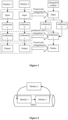
- Figure 3 is a schematic diagram showing a resource integrating process according to an embodiment of the present disclosure. The integration includes: arithmetic unit integration and framework integration. In practice, overall resources can be reduced by about 8% after the resources occupied by modules are integrated.
- the arithmetic unit includes a multiplier, an adder and other computers that can be implemented by a DSP.
- the convolution layer of the CNN mainly involves convolution computation which includes multiplication and addition and is suitable for arithmetic unit integration.
- the models in the mathematical library of the CAFFE model also include dot-multiplication, addition-multiplication, zoom, multiplication-addition, and the like, which contain multiplication operations and addition operations that may be reused.
- the integrating method is illustrated as follows. 1. Addition and multiplication in multiple modules are specified to use the same adder and the same multiplier.
- the arithmetic c in module 1 and the arithmetic c in module 2 are implemented by reusing one arithmetic c. 2.
- a time delay cannot be met when sharing the arithmetic, it may be tried to merge the modules, implement a variety of functions together, and share inputs and outputs.
- two arithmetical modules when deployed on the FPGA, are spaced far apart on elements of the printed circuit board (PCB), if only one of the components is reused, a circuit delay does not meet the standard. In this case, the whole arithmetical module is directly merged together, so that the resources may be reused.
- interface resources of the FPGA are occupied by inputs and outputs of multiple modules, which resulting in consuming of LUT resources of the FPGA, therefore, many modules with the same or similar input format and output format may be merged to reduce a waste of resources caused by the inputs and the outputs.
- the addition, subtraction, multiplication, division and the like in the mathematical library of the CAFFE model which have some differences in arithmetic with each other and have similar interfaces, not only the arithmetic unit integration but also the module framework integration can be implemented after the modules are merged.
- An integrating method are described as follows. 1. Modules having the same or similar (that is, difference lies in a parameter) input and output interfaces are found from the computation module.
- the same input and output interfaces indicate that the outputs are 32-bit integers, or 64-bit integers, that is, inputs and outputs are the same, the similar input and output interfaces indicate that a 64-bit interface is compatible for a 32-bit interface, and belong to similar modules.
- Module functions are merged into a large module, and the identical computation resources are integrated (that is, to achieve the arithmetic unit integration), for example, in Figure 3 , the two input interfaces are merged into an input interface, the two output interfaces are merged into an output interface. 3. It is determined whether to skip or perform a part of the similar modules with different parameters based on a conditional judgment.
- an input of the function A is 1, 2
- an input of the function B is 1, 2, 3
- an input of the merged AB is 1, 2, 3.
- the function A is implemented only when the input 3 is invalid. A condition judgment is required to judge the scope of 3, and the function A is different from the function B, it is skipped between the function modules based on whether the 3 is invalid or valid.
- the CNN includes multiple modules, in the iterative process, not all modules are in a computation state, and there is an order of executing the modules. For example, in a Mnist model, cyclic iterative computation is performed between the convolution layer, the pool layer, the complete connection layer and the like. FPGA resources are limited, and cannot deploy all the modules of the whole CNN model in general. Delay of computation between modules may be used, a module completing computation may be switched to a module to be computed during an operation of a module, to implement the switch continuously, thereby achieving deployment and computation of all the modules in the CNN. As shown in Figure 4a, which is a schematic diagram showing module switching according to an embodiment of the present disclosure.
- the module switching method and the effect evaluation include the following step 1 to step 4.
- the CNN model is illustrated to include three modules (which are a module 1, a module 2 and a module 3).
- the module 1 and the module 2 are employed by the FPGA first, and computation is began, operating time of the two modules are t1 and t2 respectively.
- step 2 an operation state of the modules on the FPGA is monitored.
- the module 2 is operated after the module 1 completes operation.
- the module 1 is unloaded, and the module 3 is loaded, operating time of the module 3 is t3, and loading time of each of the module 1, the module 2 and the module 3 is T.
- step 3 the above process is repeated, switch and operating are performed among the multiple modules on the FPGA.
- step 4 if the loading time T is less than t1, t2, t3, there is no delay for each switch.
- a related device for carrying out the above-described solutions is provided in order to better implement the above-described solutions of the present disclosure.
- a CNN processing device 500 is provided according to an embodiment of the present disclosure, which may include a type acquiring unit 501, a deploying unit 502, a merging unit 503 and a module operating unit 504.
- the type acquiring unit 501 is configured to acquire an intensity type of a first module in a CNN model.
- the deploying unit 502 is configured to, in a case that the intensity type of the first module is a computation-intensity type, deploy the first module on a field programmable gate array, FPGA, and acquire multiple arithmetic unit resources of the FPGA which are occupied by the first module.
- the intensity type of the first module is a computation-intensity type
- the merging unit 503 is configured to obtain a first resource merging module by merging identical arithmetic unit resources among the multiple arithmetic unit resources of the FPGA which are occupied by the first module.
- the module operating unit 504 is configured to operate the first resource merging module by the FPGA to recognize an image.
- the type acquiring unit 501 is further configured to acquire an intensity type of a second module in the CNN model.
- the deploying unit 502 is further configured to deploy the second module on the FPGA and acquire multiple arithmetic unit resources of the FPGA which are occupied by the second module, in a case that the intensity type of the second module is the computation-intensity type.
- the merging unit 503 is further configured to merge the first module and the second module to obtain a third module in a case that the arithmetic unit resources occupied by the first module are identical or partially identical to the arithmetic unit resources occupied by the second module, where a function of the third module includes a function of the first module and a function of the second module.
- the module operating unit 504 is further configured to operate the third module by the FPGA.
- the merging unit 504 is further configured to reuse identical arithmetic unit resources of the FPGA which are occupied by the first module and the second module, and merge an input interface of the first module and an input interface of the second module, and merge an output interface of the first module and an output interface of the second module.
- the module operating unit 504 is configured to set a come into effect condition for the function of the third module based on the function of the first module and the function of the second module, and determine whether to implement the function of the first module or the function of the second module by the FPGA based on the come into effect condition.
- the merging unit 503 is further configured to obtain a second resource merging module by merging identical arithmetic unit resources among the multiple arithmetic unit resources of the FPGA which are occupied by the second module.
- the module operating unit 503 is further configured to operate the second resource merging module by the FPGA.
- the CNN processing device 500 further includes a module switching unit 505 configured to: monitor an operation state of the first resource merging module on the FPGA during operating the first resource merging module by the FPGA; unload the first resource merging module from the FPGA after the first resource merging module completes operation on the FPGA; and load a fourth module in the CNN model to the FPGA.
- a module switching unit 505 configured to: monitor an operation state of the first resource merging module on the FPGA during operating the first resource merging module by the FPGA; unload the first resource merging module from the FPGA after the first resource merging module completes operation on the FPGA; and load a fourth module in the CNN model to the FPGA.
- the deploying unit 502 is further configured to deploy a mathematical library of the CNN model on the FPGA, where the mathematical library includes the first module.
- the FPGA is a field programmable gate array FPGA.
- an intensity type of a first module in a CNN model is acquired firstly, the first module is deployed on an FPGA and multiple arithmetic unit resources of the FPGA which are occupied by the first module are acquired in a case that the intensity type of the first module is a computation-intensity type, identical arithmetic unit resources among the multiple arithmetic unit resources of the FPGA which are occupied by the first module are merged to obtain the first module deployed on the FPGA in which arithmetic unit resources are merged, and the first module deployed on the FPGA in which arithmetic unit resources are merged is operated.
- the first module of the computation-intensity type may be migrated to the FPGA, so that module arithmetic in the CNN model is implemented by the FPGA without using the GPU, while both a deployment cost and an operation cost of the FPGA are much less than that of the GPU.
- the identical arithmetic unit resources in the first module of the computation-intensity type are merged, so that the arithmetic unit resources are utilized with a highest use efficiency, and thus, the computation performance of the CNN can be ensured.
- FIG. 6 is a schematic diagram showing a structure of a server according to an embodiment of the present disclosure.
- the server 600 may vary considerably depending on a configuration or a performance and may include one or more central processing units (CPU) 622 (e.g., one or more processors), a memory 632, one or more storage medium 630 (e.g., one or more mass storage devices) that store an application 642 or data 644, and FPGA 633.
- the memory 632 and the storage medium 630 may be temporary storages or persistent storages.
- Programs stored in the storage medium 630 may include one or more modules (not shown in the drawing), each of the modules may include a series of instruction operations on the server.
- the central processing unit 622 may be configured to communicate with the storage medium 630 to perform the series of instruction operations in the storage medium 630 on the server 600.
- the server 600 may further include one or more power supplies 626, one or more wired or wireless network interfaces 650, one or more input and output interfaces 658, and/or one or more operating systems 641, such as Windows ServerTM, Mac OS XTM, UnixTM, LinuxTM, and FreeBSDTM.
- the steps performed by the server in the above-described embodiment may be based on the structure of the server shown in Figure 6 , which may perform the above-described CNN processing method, as described in the description of the above-described embodiments.
- connection relation between the modules indicates that there is a communication connection between the modules, and may be embodied as one or more communication buses or signal lines.
- the present disclosure can be implemented by software and necessary general-purpose hardware, and may also be implemented by dedicated hardware including an application specific integrated circuit, a dedicated CPU, a dedicated memory, a dedicated component.
- functions implemented by a computer program can be easily implemented by the appropriate hardware, and a specific hardware structure used to implement the same function can be varied, such as an analog circuit, a digital circuit, or a dedicated circuit.
- an implementation by a software program is a better embodiment for the present disclosure.
- the technical solution of the present disclosure or a part of the technical solution making a contribution to the prior art may be embodied in the form of a software product stored in a readable storage medium, such as a floppy disk of a computer, a USB disk, a mobile hard disk, a read-only memory (ROM), a random access memory (RAM), a magnetic disk, or an optical disk, and the software product includes several instructions for causing a computer device (which may be a personal computer, a server, a network device, or the like) to perform method described in various embodiments of the present disclosure that fall within the scope of the appended claims.
- a computer device which may be a personal computer, a server, a network device, or the like
Landscapes
- Engineering & Computer Science (AREA)
- Physics & Mathematics (AREA)
- Theoretical Computer Science (AREA)
- Health & Medical Sciences (AREA)
- Life Sciences & Earth Sciences (AREA)
- Biomedical Technology (AREA)
- Biophysics (AREA)
- Software Systems (AREA)
- General Physics & Mathematics (AREA)
- General Engineering & Computer Science (AREA)
- Computing Systems (AREA)
- Artificial Intelligence (AREA)
- General Health & Medical Sciences (AREA)
- Evolutionary Computation (AREA)
- Data Mining & Analysis (AREA)
- Mathematical Physics (AREA)
- Computational Linguistics (AREA)
- Molecular Biology (AREA)
- Neurology (AREA)
- Image Analysis (AREA)
- Stored Programmes (AREA)
- Management, Administration, Business Operations System, And Electronic Commerce (AREA)
- User Interface Of Digital Computer (AREA)
- Testing And Monitoring For Control Systems (AREA)
- Design And Manufacture Of Integrated Circuits (AREA)
- Feedback Control In General (AREA)
Claims (11)
- Procédé de traitement de réseau neuronal convolutionnel, CNN, comprenant :l'acquisition d'un type d'intensité d'un premier module dans un modèle CNN (101), le type d'intensité du premier module dans le modèle CNN (101) étant un type déterminé sur la base d'un degré d'intensité de calcul d'une couche du réseau neuronal convolutionnel ;dans un cas où le type d'intensité du premier module est un type d'intensité de calcul, le déploiement du premier module sur un réseau de portes programmable (FPGA), et l'acquisition d'une pluralité de ressources unitaires arithmétiques du FPGA qui sont occupées par le premier module (102) ;l'obtention d'un premier module de fusion de ressources en fusionnant des ressources unitaires arithmétiques identiques, parmi la pluralité de ressources unitaires arithmétiques du FPGA qui sont occupées par le premier module (103) ; etle fonctionnement du premier module de fusion de ressources par le FPGA (104) ;l'acquisition d'un type d'intensité d'un deuxième module dans le modèle CNN (101), le type d'intensité du deuxième module dans le modèle CNN (101) étant un type déterminé sur la base d'un degré d'intensité de calcul d'une couche du réseau neuronal convolutionnel ;dans un cas où le type d'intensité du deuxième module est un type d'intensité de calcul, le déploiement du deuxième module sur le FPGA et l'acquisition d'une pluralité de ressources unitaires arithmétiques du FPGA qui sont occupées par le deuxième module ;dans un cas où les ressources unitaires arithmétiques occupées par le premier module sont identiques ou partiellement identiques aux ressources unitaires arithmétiques occupées par le deuxième module, la fusion du premier module et du deuxième module pour obtenir un troisième module, dans lequel une fonction du troisième module comprend une fonction du premier module et une fonction du deuxième module ; etle fonctionnement du troisième module par le FPGA, dans lequel la fusion du premier module et du deuxième module comprend :la réutilisation des ressources unitaires arithmétiques identiques du FPGA qui sont occupées par le premier module et le deuxième module ; etla fusion d'une interface d'entrée du premier module et d'une interface d'entrée du deuxième module, et la fusion d'une interface de sortie du premier module et d'une interface de sortie du deuxième module.
- Procédé selon la revendication 1, dans lequel le fonctionnement du troisième module par le FPGA comprend :la définition d'une condition d'entrée en vigueur pour la fonction du troisième module sur la base de la fonction du premier module et de la fonction du deuxième module, dans lequel la condition d'entrée en vigueur est utilisée pour déterminer dans quel cas le troisième module met en œuvre la fonction du premier module et dans quel cas le troisième module met en œuvre la fonction du deuxième module ; etla mise en oeuvre, par le FPGA, de la fonction du premier module ou de la fonction du deuxième module correspondant à la condition d'entrée en vigueur.
- Procédé selon la revendication 1, dans lequel, après le déploiement du deuxième module sur le FPGA et l'acquisition de la pluralité de ressources unitaires arithmétiques du FPGA qui sont occupées par le deuxième module, le procédé comprend en outre :l'obtention d'un deuxième module de fusion de ressources en fusionnant des ressources unitaires arithmétiques identiques, parmi la pluralité de ressources unitaires arithmétiques du FPGA qui sont occupées par le deuxième module ; etle fonctionnement du deuxième module de fusion de ressources par le FPGA.
- Procédé selon la revendication 1 comprenant en outre ;la surveillance d'un état de fonctionnement du premier module de fusion de ressources sur le FPGA pendant le fonctionnement du premier module de fusion de ressources par le FPGA ;le déchargement du premier module de fusion de ressources du FPGA après que le premier module de fusion de ressources a terminé son fonctionnement sur le FPGA ; etle chargement d'un quatrième module dans le modèle CNN sur le FPGA.
- Procédé selon la revendication 1, comprenant en outre :le déploiement d'une bibliothèque mathématique du modèle CNN sur le FPGA, dans lequella bibliothèque mathématique comprend le premier module.
- Dispositif de traitement de réseau neuronal convolutionnel, CNN, comprenant :une unité d'acquisition de type (501) configurée pour acquérir un type d'intensité d'un premier module dans un modèle CNN ;une unité de déploiement (502) configurée pour, dans un cas où le type d'intensité du premier module est un type d'intensité de calcul, déployer le premier module sur un réseau de portes programmable, FPGA, et acquérir une pluralité de ressources unitaires arithmétiques du FPGA qui sont occupées par le premier module ;une unité de fusion (503) configurée pour obtenir un premier module de fusion de ressources en fusionnant des ressources unitaires arithmétiques identiques, parmi la pluralité de ressources unitaires arithmétiques du FPGA qui sont occupées par le premier module ; etune unité de fonctionnement de module (504) configurée pour faire fonctionner le premier module de fusion de ressources par le FPGA,dans lequel l'unité d'acquisition de type (501) est en outre configurée pour acquérir un type d'intensité d'un deuxième module dans le modèle CNN,l'unité de déploiement (502) est en outre configurée pour, dans un cas où le type d'intensité du deuxième module est le type d'intensité de calcul, déployer le deuxième module sur le FPGA et acquérir une pluralité de ressources unitaires arithmétiques du FPGA qui sont occupées par le deuxième module,l'unité de fusion (503) est en outre configurée pour, dans un cas où les ressources unitaires arithmétiques occupées par le premier module sont identiques ou partiellement identiques aux ressources unitaires arithmétiques occupées par le deuxième module, fusionner le premier module et le deuxième module pour obtenir un troisième module, dans lequel une fonction du troisième module comprend une fonction du premier module et une fonction du deuxième module, etl'unité de fonctionnement de module (504) est en outre configurée pour faire fonctionner le troisième module par le FPGA, dans lequel l'unité de fusion (503) est en outre configurée pour :réutiliser des ressources unitaires arithmétiques identiques du FPGA qui sont occupées par le premier module et le deuxième module ; etfusionner une interface d'entrée du premier module et une interface d'entrée du deuxième module, et fusionner une interface de sortie du premier module et une interface de sortie du deuxième module.
- Dispositif selon la revendication 6, dans lequel l'unité de fonctionnement de module (504) est en outre configurée pour :définir une condition d'entrée en vigueur pour la fonction du troisième module sur la base de la fonction du premier module et de la fonction du deuxième module, dans lequel la condition d'entrée en vigueur est utilisée pour déterminer dans quel cas le troisième module met en œuvre la fonction du premier module et dans quel cas le troisième module met en œuvre la fonction du deuxième module ; etmettre en oeuvre, par le FPGA, la fonction du premier module ou la fonction du deuxième module correspondant à la condition d'entrée en vigueur.
- Dispositif selon la revendication 6, dans lequel l'unité de fusion (503) est en outre configurée pour obtenir un deuxième module de fusion de ressources en fusionnant des ressources unitaires arithmétiques identiques, parmi la pluralité de ressources unitaires arithmétiques du FPGA qui sont occupées par le deuxième module ; et
l'unité de fonctionnement de module (504) est en outre configurée pour faire fonctionner le deuxième module de fusion de ressources par le FPGA. - Dispositif selon la revendication 6, comprenant en outre une unité de commutation de module (505) configurée pour :surveiller un état de fonctionnement du premier module de fusion sur le FPGA pendant le fonctionnement du premier module de fusion de ressources par le FPGA ;décharger le premier module de fusion de ressources du FPGA après que le premier module de fusion de ressources a terminé son fonctionnement sur le FPGA ; etcharger un quatrième module dans le modèle CNN sur le FPGA.
- Dispositif selon la revendication 6, dans lequel l'unité de déploiement (502) est en outre configurée pour déployer une bibliothèque mathématique du modèle CNN sur le FPGA, dans lequel la bibliothèque mathématique comprend le premier module.
- Support de stockage non volatil comprenant un ou plusieurs programmes informatiques, dans lequel les programmes informatiques comprennent des instructions pouvant être exécutées par un processeur comprenant une ou plusieurs mémoires, dans lequel, lorsqu'elles sont exécutées par un ordinateur, lesdites instructions amènent ledit ordinateur à réaliser le procédé de traitement de réseau neuronal convolutionnel selon l'une quelconque des revendications 1 à 5.
Applications Claiming Priority (2)
| Application Number | Priority Date | Filing Date | Title |
|---|---|---|---|
| CN201610017755.1A CN105678379B (zh) | 2016-01-12 | 2016-01-12 | 一种cnn的处理方法和装置 |
| PCT/CN2017/070628 WO2017121297A1 (fr) | 2016-01-12 | 2017-01-09 | Procédé et dispositif de traitement cnn |
Publications (3)
| Publication Number | Publication Date |
|---|---|
| EP3404587A1 EP3404587A1 (fr) | 2018-11-21 |
| EP3404587A4 EP3404587A4 (fr) | 2019-10-30 |
| EP3404587B1 true EP3404587B1 (fr) | 2023-11-01 |
Family
ID=56300134
Family Applications (1)
| Application Number | Title | Priority Date | Filing Date |
|---|---|---|---|
| EP17738111.8A Active EP3404587B1 (fr) | 2016-01-12 | 2017-01-09 | Procédé et dispositif de traitement cnn |
Country Status (9)
| Country | Link |
|---|---|
| US (1) | US11151442B2 (fr) |
| EP (1) | EP3404587B1 (fr) |
| JP (1) | JP6507271B2 (fr) |
| KR (1) | KR102192468B1 (fr) |
| CN (1) | CN105678379B (fr) |
| CA (1) | CA2987325C (fr) |
| MY (1) | MY188759A (fr) |
| SG (1) | SG11201709689PA (fr) |
| WO (1) | WO2017121297A1 (fr) |
Families Citing this family (37)
| Publication number | Priority date | Publication date | Assignee | Title |
|---|---|---|---|---|
| CN105678379B (zh) * | 2016-01-12 | 2020-08-07 | 腾讯科技(深圳)有限公司 | 一种cnn的处理方法和装置 |
| CN106228240B (zh) * | 2016-07-30 | 2020-09-01 | 复旦大学 | 基于fpga的深度卷积神经网络实现方法 |
| KR102835519B1 (ko) * | 2016-09-28 | 2025-07-17 | 에스케이하이닉스 주식회사 | 합성곱 신경망의 연산 장치 및 방법 |
| US10733505B2 (en) | 2016-11-10 | 2020-08-04 | Google Llc | Performing kernel striding in hardware |
| WO2018113597A1 (fr) * | 2016-12-20 | 2018-06-28 | 上海寒武纪信息科技有限公司 | Dispositif de multiplication et d'addition de matrices, dispositif d'informatique neuronale et procédé |
| US11238334B2 (en) | 2017-04-04 | 2022-02-01 | Hailo Technologies Ltd. | System and method of input alignment for efficient vector operations in an artificial neural network |
| US12430543B2 (en) | 2017-04-04 | 2025-09-30 | Hailo Technologies Ltd. | Structured sparsity guided training in an artificial neural network |
| US11551028B2 (en) | 2017-04-04 | 2023-01-10 | Hailo Technologies Ltd. | Structured weight based sparsity in an artificial neural network |
| US10387298B2 (en) | 2017-04-04 | 2019-08-20 | Hailo Technologies Ltd | Artificial neural network incorporating emphasis and focus techniques |
| US11615297B2 (en) | 2017-04-04 | 2023-03-28 | Hailo Technologies Ltd. | Structured weight based sparsity in an artificial neural network compiler |
| US11544545B2 (en) | 2017-04-04 | 2023-01-03 | Hailo Technologies Ltd. | Structured activation based sparsity in an artificial neural network |
| US10467795B2 (en) * | 2017-04-08 | 2019-11-05 | Intel Corporation | Sub-graph in frequency domain and dynamic selection of convolution implementation on a GPU |
| CN107491809B (zh) * | 2017-08-21 | 2020-10-16 | 苏州浪潮智能科技有限公司 | 一种fpga实现残差网络中激活函数的方法 |
| CN108021938A (zh) * | 2017-11-29 | 2018-05-11 | 中冶南方工程技术有限公司 | 一种冷轧带钢表面缺陷在线检测方法以及检测系统 |
| JP6574004B2 (ja) * | 2018-01-25 | 2019-09-11 | 株式会社モルフォ | 計算手法決定システム、計算手法決定装置、処理装置、計算手法決定方法、処理方法、計算手法決定プログラム、及び、処理プログラム |
| CN108470211B (zh) * | 2018-04-09 | 2022-07-12 | 郑州云海信息技术有限公司 | 一种卷积计算的实现方法、设备和计算机存储介质 |
| CN110533666B (zh) * | 2018-05-25 | 2022-09-23 | 杭州海康威视数字技术股份有限公司 | 一种获取数据块尺寸的方法、处理数据的方法及装置 |
| CN108805285B (zh) * | 2018-05-30 | 2022-03-29 | 山东浪潮科学研究院有限公司 | 一种卷积神经网络池化单元设计方法 |
| US11960935B2 (en) | 2018-06-27 | 2024-04-16 | Amazon Technologies, Inc. | Fault-tolerant accelerator based inference service |
| EP3814899B1 (fr) * | 2018-06-27 | 2022-11-23 | Amazon Technologies, Inc. | Service d'inférence basé sur un accélérateur annexé |
| CN109165736B (zh) * | 2018-08-08 | 2023-12-12 | 北京字节跳动网络技术有限公司 | 应用于卷积神经网络的信息处理方法和装置 |
| KR101984730B1 (ko) * | 2018-10-23 | 2019-06-03 | (주) 글루시스 | 서버 장애 자동 예측 시스템 및 자동 예측 방법 |
| CN111488216B (zh) * | 2019-01-28 | 2024-04-30 | 北京灵汐科技有限公司 | 一种数据处理的方法、装置及电子设备 |
| CN110032374B (zh) * | 2019-03-21 | 2023-04-07 | 深兰科技(上海)有限公司 | 一种参数提取方法、装置、设备及介质 |
| CN110555519B (zh) * | 2019-10-08 | 2023-07-28 | 东南大学 | 一种基于符号随机计算的低复杂度卷积神经网络架构 |
| CN111767059B (zh) * | 2020-06-30 | 2023-03-31 | 北京百度网讯科技有限公司 | 深度学习模型的部署方法、装置、电子设备和存储介质 |
| CN111915016B (zh) * | 2020-07-10 | 2022-03-25 | 深圳云天励飞技术股份有限公司 | 一种基于tvm编译器的异构平台的部署方法及装置 |
| CN111984864B (zh) * | 2020-08-14 | 2023-12-26 | 北京达佳互联信息技术有限公司 | 对象推荐方法、装置、电子设备和存储介质 |
| US11811421B2 (en) | 2020-09-29 | 2023-11-07 | Hailo Technologies Ltd. | Weights safety mechanism in an artificial neural network processor |
| US11263077B1 (en) | 2020-09-29 | 2022-03-01 | Hailo Technologies Ltd. | Neural network intermediate results safety mechanism in an artificial neural network processor |
| US11874900B2 (en) | 2020-09-29 | 2024-01-16 | Hailo Technologies Ltd. | Cluster interlayer safety mechanism in an artificial neural network processor |
| US12248367B2 (en) | 2020-09-29 | 2025-03-11 | Hailo Technologies Ltd. | Software defined redundant allocation safety mechanism in an artificial neural network processor |
| US11237894B1 (en) | 2020-09-29 | 2022-02-01 | Hailo Technologies Ltd. | Layer control unit instruction addressing safety mechanism in an artificial neural network processor |
| US11221929B1 (en) | 2020-09-29 | 2022-01-11 | Hailo Technologies Ltd. | Data stream fault detection mechanism in an artificial neural network processor |
| JP7513189B2 (ja) * | 2021-03-05 | 2024-07-09 | 日本電信電話株式会社 | スケジューリング装置、スケジューリング方法、および、スケジューリングプログラム |
| US12210962B2 (en) * | 2021-06-30 | 2025-01-28 | Micron Technology, Inc. | Artificial neural networks on a deep learning accelerator |
| CN116700912B (zh) * | 2022-02-28 | 2025-03-25 | 华为技术有限公司 | 一种访问逻辑ip的软硬件交互方法及装置 |
Family Cites Families (22)
| Publication number | Priority date | Publication date | Assignee | Title |
|---|---|---|---|---|
| JP4212676B2 (ja) * | 1998-02-12 | 2009-01-21 | 富士ゼロックス株式会社 | 情報処理システムおよび情報処理方法 |
| US20080228719A1 (en) * | 2007-03-13 | 2008-09-18 | Fatdoor, Inc. | People and business search result optimization |
| JP2008235992A (ja) * | 2007-03-16 | 2008-10-02 | Matsushita Electric Ind Co Ltd | リコンフィギュラブル回路、リコンフィギュラブル回路システムおよびリコンフィギュラブル回路の配置配線方法 |
| US8694948B2 (en) * | 2008-11-28 | 2014-04-08 | Nec Corporation | Reconfigurable circuit generation device, method, and program |
| US8442927B2 (en) * | 2009-07-30 | 2013-05-14 | Nec Laboratories America, Inc. | Dynamically configurable, multi-ported co-processor for convolutional neural networks |
| CN102799563B (zh) * | 2011-05-26 | 2015-08-26 | 上海红神信息技术有限公司 | 一种可重构计算阵列及构建方法 |
| US10860946B2 (en) * | 2011-08-10 | 2020-12-08 | Konlanbi | Dynamic data structures for data-driven modeling |
| US20130132962A1 (en) * | 2011-11-22 | 2013-05-23 | Microsoft Corporation | Scheduler combinators |
| GB2516627A (en) * | 2013-07-26 | 2015-02-04 | Warsaw University Of Technology | Parallel decision-or regression-tree growing |
| US10042894B2 (en) * | 2013-10-31 | 2018-08-07 | Microsoft Technology Licensing, Llc | Temporal-based professional similarity |
| US9978014B2 (en) | 2013-12-18 | 2018-05-22 | Intel Corporation | Reconfigurable processing unit |
| CN104077233B (zh) * | 2014-06-18 | 2017-04-05 | 百度在线网络技术(北京)有限公司 | 多通道卷积层处理方法和装置 |
| CN104035751B (zh) * | 2014-06-20 | 2016-10-12 | 深圳市腾讯计算机系统有限公司 | 基于多图形处理器的数据并行处理方法及装置 |
| JP6381368B2 (ja) * | 2014-08-26 | 2018-08-29 | キヤノン株式会社 | 画像処理装置、画像処理方法、およびプログラム |
| CN104287764B (zh) * | 2014-09-11 | 2017-05-31 | 沈阳东软医疗系统有限公司 | 一种ct灌注成像方法和设备 |
| US20160314410A1 (en) * | 2015-04-23 | 2016-10-27 | Rovi Guides, Inc. | Systems and methods for improving accuracy in media asset recommendations based on data from one data space |
| CN104915195B (zh) * | 2015-05-20 | 2017-11-28 | 清华大学 | 一种基于现场可编程门阵列实现神经网络计算的方法 |
| CN104915322B (zh) * | 2015-06-09 | 2018-05-01 | 中国人民解放军国防科学技术大学 | 一种卷积神经网络硬件加速方法 |
| US10579628B2 (en) * | 2015-12-17 | 2020-03-03 | The Nielsen Company (Us), Llc | Media names matching and normalization |
| CN105678379B (zh) * | 2016-01-12 | 2020-08-07 | 腾讯科技(深圳)有限公司 | 一种cnn的处理方法和装置 |
| US9903733B2 (en) * | 2016-03-17 | 2018-02-27 | Honda Motor Co., Ltd. | Vehicular communications network and methods of use and manufacture thereof |
| CN106709532B (zh) * | 2017-01-25 | 2020-03-10 | 京东方科技集团股份有限公司 | 图像处理方法和装置 |
-
2016
- 2016-01-12 CN CN201610017755.1A patent/CN105678379B/zh active Active
-
2017
- 2017-01-09 WO PCT/CN2017/070628 patent/WO2017121297A1/fr not_active Ceased
- 2017-01-09 KR KR1020177035657A patent/KR102192468B1/ko active Active
- 2017-01-09 CA CA2987325A patent/CA2987325C/fr active Active
- 2017-01-09 MY MYPI2017704511A patent/MY188759A/en unknown
- 2017-01-09 EP EP17738111.8A patent/EP3404587B1/fr active Active
- 2017-01-09 SG SG11201709689PA patent/SG11201709689PA/en unknown
- 2017-01-09 JP JP2017564718A patent/JP6507271B2/ja active Active
- 2017-11-27 US US15/822,627 patent/US11151442B2/en active Active
Also Published As
| Publication number | Publication date |
|---|---|
| EP3404587A1 (fr) | 2018-11-21 |
| KR20180005241A (ko) | 2018-01-15 |
| US11151442B2 (en) | 2021-10-19 |
| JP6507271B2 (ja) | 2019-04-24 |
| US20180082175A1 (en) | 2018-03-22 |
| CA2987325A1 (fr) | 2017-07-20 |
| CN105678379B (zh) | 2020-08-07 |
| WO2017121297A1 (fr) | 2017-07-20 |
| SG11201709689PA (en) | 2017-12-28 |
| CA2987325C (fr) | 2019-10-22 |
| EP3404587A4 (fr) | 2019-10-30 |
| MY188759A (en) | 2021-12-29 |
| JP2018526714A (ja) | 2018-09-13 |
| CN105678379A (zh) | 2016-06-15 |
| BR112017026917A2 (pt) | 2018-08-14 |
| KR102192468B1 (ko) | 2020-12-17 |
Similar Documents
| Publication | Publication Date | Title |
|---|---|---|
| US11151442B2 (en) | Convolutional neural network processing method and device | |
| Hannig et al. | Invasive tightly-coupled processor arrays: A domain-specific architecture/compiler co-design approach | |
| US20190179635A1 (en) | Method and apparatus for tensor and convolution operations | |
| US9590629B2 (en) | Logical elements with switchable connections | |
| Kästner et al. | Hardware/software codesign for convolutional neural networks exploiting dynamic partial reconfiguration on PYNQ | |
| CA2994188C (fr) | Puce auto-adaptative et procede de configuration | |
| CN105487838A (zh) | 一种动态可重构处理器的任务级并行调度方法与系统 | |
| US10374605B2 (en) | Logical elements with switchable connections in a reconfigurable fabric | |
| CN104375805A (zh) | 采用多核处理器仿真可重构处理器并行计算过程的方法 | |
| EP3555760A1 (fr) | Traitement en parallèle sur demande grâce à un fpga partiellement reconfigurable dynamiquement | |
| US20260010369A1 (en) | Accelerated processing device and method of sharing data for machine learning | |
| Bruel et al. | Generalize or die: Operating systems support for memristor-based accelerators | |
| CN112084023A (zh) | 数据并行处理的方法、电子设备及计算机可读存储介质 | |
| Madhu et al. | Compiling HPC kernels for the REDEFINE CGRA | |
| Li et al. | An area-efficient FPGA overlay using DSP block based time-multiplexed functional units | |
| Naik et al. | Analysis of performance enhancement on graphic processor based heterogeneous architecture: A CUDA and MATLAB experiment | |
| US20240355044A1 (en) | System and method for executing a task | |
| WO2026081311A1 (fr) | Procédé d'attribution de ressources informatiques matérielles, ressource informatique matérielle et dispositif électronique | |
| Hong et al. | Efficient on-chip task scheduler and allocator for reconfigurable operating systems | |
| CN116400926A (zh) | 面向人工智能芯片的标量引擎处理方法和装置 | |
| Chen et al. | High throughput and low bandwidth demand: Accelerating CNN inference Block-by-block on FPGAs | |
| EP4645074A1 (fr) | Accélérateur de mélange pour unité de traitement graphique | |
| Li et al. | A Deep Learning Prediction Process Based on Low-power Heterogeneous Multi Core Architecture | |
| Moghaddam et al. | Design and implementation of high performance architectures with partially reconfigurable cgras | |
| CN121660114A (zh) | 混合专家模型的专家网络处理方法及其装置、设备和介质 |
Legal Events
| Date | Code | Title | Description |
|---|---|---|---|
| STAA | Information on the status of an ep patent application or granted ep patent |
Free format text: STATUS: THE INTERNATIONAL PUBLICATION HAS BEEN MADE |
|
| PUAI | Public reference made under article 153(3) epc to a published international application that has entered the european phase |
Free format text: ORIGINAL CODE: 0009012 |
|
| STAA | Information on the status of an ep patent application or granted ep patent |
Free format text: STATUS: REQUEST FOR EXAMINATION WAS MADE |
|
| 17P | Request for examination filed |
Effective date: 20171227 |
|
| AK | Designated contracting states |
Kind code of ref document: A1 Designated state(s): AL AT BE BG CH CY CZ DE DK EE ES FI FR GB GR HR HU IE IS IT LI LT LU LV MC MK MT NL NO PL PT RO RS SE SI SK SM TR |
|
| AX | Request for extension of the european patent |
Extension state: BA ME |
|
| DAV | Request for validation of the european patent (deleted) | ||
| DAX | Request for extension of the european patent (deleted) | ||
| A4 | Supplementary search report drawn up and despatched |
Effective date: 20191002 |
|
| RIC1 | Information provided on ipc code assigned before grant |
Ipc: G06F 9/50 20060101ALI20190926BHEP Ipc: G06N 3/04 20060101ALI20190926BHEP Ipc: G06N 3/06 20060101AFI20190926BHEP Ipc: G06N 3/063 20060101ALI20190926BHEP |
|
| STAA | Information on the status of an ep patent application or granted ep patent |
Free format text: STATUS: EXAMINATION IS IN PROGRESS |
|
| 17Q | First examination report despatched |
Effective date: 20210519 |
|
| RAP3 | Party data changed (applicant data changed or rights of an application transferred) |
Owner name: TENCENT TECHNOLOGY (SHENZHEN) COMPANY LIMITED |
|
| REG | Reference to a national code |
Ref legal event code: R079 Ipc: G06F0009500000 Ref country code: DE Ref legal event code: R079 Ref document number: 602017075982 Country of ref document: DE Free format text: PREVIOUS MAIN CLASS: G06N0003060000 Ipc: G06F0009500000 |
|
| GRAP | Despatch of communication of intention to grant a patent |
Free format text: ORIGINAL CODE: EPIDOSNIGR1 |
|
| STAA | Information on the status of an ep patent application or granted ep patent |
Free format text: STATUS: GRANT OF PATENT IS INTENDED |
|
| RIC1 | Information provided on ipc code assigned before grant |
Ipc: G06N 3/045 20230101ALI20230508BHEP Ipc: G06N 3/063 20060101ALI20230508BHEP Ipc: G06N 3/04 20060101ALI20230508BHEP Ipc: G06F 9/50 20060101ALI20230508BHEP Ipc: G06N 3/06 20060101AFI20230508BHEP |
|
| RIC1 | Information provided on ipc code assigned before grant |
Ipc: G06N 3/0464 20230101ALI20230517BHEP Ipc: G06N 3/045 20230101ALI20230517BHEP Ipc: G06N 3/063 20060101ALI20230517BHEP Ipc: G06F 9/50 20060101AFI20230517BHEP |
|
| INTG | Intention to grant announced |
Effective date: 20230601 |
|
| GRAS | Grant fee paid |
Free format text: ORIGINAL CODE: EPIDOSNIGR3 |
|
| GRAA | (expected) grant |
Free format text: ORIGINAL CODE: 0009210 |
|
| STAA | Information on the status of an ep patent application or granted ep patent |
Free format text: STATUS: THE PATENT HAS BEEN GRANTED |
|
| AK | Designated contracting states |
Kind code of ref document: B1 Designated state(s): AL AT BE BG CH CY CZ DE DK EE ES FI FR GB GR HR HU IE IS IT LI LT LU LV MC MK MT NL NO PL PT RO RS SE SI SK SM TR |
|
| REG | Reference to a national code |
Ref country code: GB Ref legal event code: FG4D |
|
| REG | Reference to a national code |
Ref country code: CH Ref legal event code: EP |
|
| REG | Reference to a national code |
Ref country code: IE Ref legal event code: FG4D |
|
| REG | Reference to a national code |
Ref country code: DE Ref legal event code: R096 Ref document number: 602017075982 Country of ref document: DE |
|
| REG | Reference to a national code |
Ref country code: LT Ref legal event code: MG9D |
|
| REG | Reference to a national code |
Ref country code: NL Ref legal event code: MP Effective date: 20231101 |
|
| PG25 | Lapsed in a contracting state [announced via postgrant information from national office to epo] |
Ref country code: GR Free format text: LAPSE BECAUSE OF FAILURE TO SUBMIT A TRANSLATION OF THE DESCRIPTION OR TO PAY THE FEE WITHIN THE PRESCRIBED TIME-LIMIT Effective date: 20240202 |
|
| PG25 | Lapsed in a contracting state [announced via postgrant information from national office to epo] |
Ref country code: IS Free format text: LAPSE BECAUSE OF FAILURE TO SUBMIT A TRANSLATION OF THE DESCRIPTION OR TO PAY THE FEE WITHIN THE PRESCRIBED TIME-LIMIT Effective date: 20240301 |
|
| PG25 | Lapsed in a contracting state [announced via postgrant information from national office to epo] |
Ref country code: LT Free format text: LAPSE BECAUSE OF FAILURE TO SUBMIT A TRANSLATION OF THE DESCRIPTION OR TO PAY THE FEE WITHIN THE PRESCRIBED TIME-LIMIT Effective date: 20231101 |
|
| REG | Reference to a national code |
Ref country code: AT Ref legal event code: MK05 Ref document number: 1627994 Country of ref document: AT Kind code of ref document: T Effective date: 20231101 |
|
| PG25 | Lapsed in a contracting state [announced via postgrant information from national office to epo] |
Ref country code: NL Free format text: LAPSE BECAUSE OF FAILURE TO SUBMIT A TRANSLATION OF THE DESCRIPTION OR TO PAY THE FEE WITHIN THE PRESCRIBED TIME-LIMIT Effective date: 20231101 |
|
| PG25 | Lapsed in a contracting state [announced via postgrant information from national office to epo] |
Ref country code: AT Free format text: LAPSE BECAUSE OF FAILURE TO SUBMIT A TRANSLATION OF THE DESCRIPTION OR TO PAY THE FEE WITHIN THE PRESCRIBED TIME-LIMIT Effective date: 20231101 |
|
| PG25 | Lapsed in a contracting state [announced via postgrant information from national office to epo] |
Ref country code: ES Free format text: LAPSE BECAUSE OF FAILURE TO SUBMIT A TRANSLATION OF THE DESCRIPTION OR TO PAY THE FEE WITHIN THE PRESCRIBED TIME-LIMIT Effective date: 20231101 |
|
| PG25 | Lapsed in a contracting state [announced via postgrant information from national office to epo] |
Ref country code: NL Free format text: LAPSE BECAUSE OF FAILURE TO SUBMIT A TRANSLATION OF THE DESCRIPTION OR TO PAY THE FEE WITHIN THE PRESCRIBED TIME-LIMIT Effective date: 20231101 Ref country code: LT Free format text: LAPSE BECAUSE OF FAILURE TO SUBMIT A TRANSLATION OF THE DESCRIPTION OR TO PAY THE FEE WITHIN THE PRESCRIBED TIME-LIMIT Effective date: 20231101 Ref country code: IS Free format text: LAPSE BECAUSE OF FAILURE TO SUBMIT A TRANSLATION OF THE DESCRIPTION OR TO PAY THE FEE WITHIN THE PRESCRIBED TIME-LIMIT Effective date: 20240301 Ref country code: GR Free format text: LAPSE BECAUSE OF FAILURE TO SUBMIT A TRANSLATION OF THE DESCRIPTION OR TO PAY THE FEE WITHIN THE PRESCRIBED TIME-LIMIT Effective date: 20240202 Ref country code: ES Free format text: LAPSE BECAUSE OF FAILURE TO SUBMIT A TRANSLATION OF THE DESCRIPTION OR TO PAY THE FEE WITHIN THE PRESCRIBED TIME-LIMIT Effective date: 20231101 Ref country code: BG Free format text: LAPSE BECAUSE OF FAILURE TO SUBMIT A TRANSLATION OF THE DESCRIPTION OR TO PAY THE FEE WITHIN THE PRESCRIBED TIME-LIMIT Effective date: 20240201 Ref country code: AT Free format text: LAPSE BECAUSE OF FAILURE TO SUBMIT A TRANSLATION OF THE DESCRIPTION OR TO PAY THE FEE WITHIN THE PRESCRIBED TIME-LIMIT Effective date: 20231101 Ref country code: PT Free format text: LAPSE BECAUSE OF FAILURE TO SUBMIT A TRANSLATION OF THE DESCRIPTION OR TO PAY THE FEE WITHIN THE PRESCRIBED TIME-LIMIT Effective date: 20240301 |
|
| PG25 | Lapsed in a contracting state [announced via postgrant information from national office to epo] |
Ref country code: SE Free format text: LAPSE BECAUSE OF FAILURE TO SUBMIT A TRANSLATION OF THE DESCRIPTION OR TO PAY THE FEE WITHIN THE PRESCRIBED TIME-LIMIT Effective date: 20231101 Ref country code: RS Free format text: LAPSE BECAUSE OF FAILURE TO SUBMIT A TRANSLATION OF THE DESCRIPTION OR TO PAY THE FEE WITHIN THE PRESCRIBED TIME-LIMIT Effective date: 20231101 Ref country code: PL Free format text: LAPSE BECAUSE OF FAILURE TO SUBMIT A TRANSLATION OF THE DESCRIPTION OR TO PAY THE FEE WITHIN THE PRESCRIBED TIME-LIMIT Effective date: 20231101 Ref country code: NO Free format text: LAPSE BECAUSE OF FAILURE TO SUBMIT A TRANSLATION OF THE DESCRIPTION OR TO PAY THE FEE WITHIN THE PRESCRIBED TIME-LIMIT Effective date: 20240201 Ref country code: LV Free format text: LAPSE BECAUSE OF FAILURE TO SUBMIT A TRANSLATION OF THE DESCRIPTION OR TO PAY THE FEE WITHIN THE PRESCRIBED TIME-LIMIT Effective date: 20231101 Ref country code: HR Free format text: LAPSE BECAUSE OF FAILURE TO SUBMIT A TRANSLATION OF THE DESCRIPTION OR TO PAY THE FEE WITHIN THE PRESCRIBED TIME-LIMIT Effective date: 20231101 |
|
| PG25 | Lapsed in a contracting state [announced via postgrant information from national office to epo] |
Ref country code: DK Free format text: LAPSE BECAUSE OF FAILURE TO SUBMIT A TRANSLATION OF THE DESCRIPTION OR TO PAY THE FEE WITHIN THE PRESCRIBED TIME-LIMIT Effective date: 20231101 |
|
| PG25 | Lapsed in a contracting state [announced via postgrant information from national office to epo] |
Ref country code: CZ Free format text: LAPSE BECAUSE OF FAILURE TO SUBMIT A TRANSLATION OF THE DESCRIPTION OR TO PAY THE FEE WITHIN THE PRESCRIBED TIME-LIMIT Effective date: 20231101 |
|
| PG25 | Lapsed in a contracting state [announced via postgrant information from national office to epo] |
Ref country code: SK Free format text: LAPSE BECAUSE OF FAILURE TO SUBMIT A TRANSLATION OF THE DESCRIPTION OR TO PAY THE FEE WITHIN THE PRESCRIBED TIME-LIMIT Effective date: 20231101 |
|
| PG25 | Lapsed in a contracting state [announced via postgrant information from national office to epo] |
Ref country code: SM Free format text: LAPSE BECAUSE OF FAILURE TO SUBMIT A TRANSLATION OF THE DESCRIPTION OR TO PAY THE FEE WITHIN THE PRESCRIBED TIME-LIMIT Effective date: 20231101 Ref country code: SK Free format text: LAPSE BECAUSE OF FAILURE TO SUBMIT A TRANSLATION OF THE DESCRIPTION OR TO PAY THE FEE WITHIN THE PRESCRIBED TIME-LIMIT Effective date: 20231101 Ref country code: IT Free format text: LAPSE BECAUSE OF FAILURE TO SUBMIT A TRANSLATION OF THE DESCRIPTION OR TO PAY THE FEE WITHIN THE PRESCRIBED TIME-LIMIT Effective date: 20231101 Ref country code: EE Free format text: LAPSE BECAUSE OF FAILURE TO SUBMIT A TRANSLATION OF THE DESCRIPTION OR TO PAY THE FEE WITHIN THE PRESCRIBED TIME-LIMIT Effective date: 20231101 Ref country code: DK Free format text: LAPSE BECAUSE OF FAILURE TO SUBMIT A TRANSLATION OF THE DESCRIPTION OR TO PAY THE FEE WITHIN THE PRESCRIBED TIME-LIMIT Effective date: 20231101 Ref country code: CZ Free format text: LAPSE BECAUSE OF FAILURE TO SUBMIT A TRANSLATION OF THE DESCRIPTION OR TO PAY THE FEE WITHIN THE PRESCRIBED TIME-LIMIT Effective date: 20231101 |
|
| REG | Reference to a national code |
Ref country code: DE Ref legal event code: R097 Ref document number: 602017075982 Country of ref document: DE |
|
| PG25 | Lapsed in a contracting state [announced via postgrant information from national office to epo] |
Ref country code: MC Free format text: LAPSE BECAUSE OF FAILURE TO SUBMIT A TRANSLATION OF THE DESCRIPTION OR TO PAY THE FEE WITHIN THE PRESCRIBED TIME-LIMIT Effective date: 20231101 |
|
| PG25 | Lapsed in a contracting state [announced via postgrant information from national office to epo] |
Ref country code: MC Free format text: LAPSE BECAUSE OF FAILURE TO SUBMIT A TRANSLATION OF THE DESCRIPTION OR TO PAY THE FEE WITHIN THE PRESCRIBED TIME-LIMIT Effective date: 20231101 |
|
| REG | Reference to a national code |
Ref country code: CH Ref legal event code: PL |
|
| PLBE | No opposition filed within time limit |
Free format text: ORIGINAL CODE: 0009261 |
|
| STAA | Information on the status of an ep patent application or granted ep patent |
Free format text: STATUS: NO OPPOSITION FILED WITHIN TIME LIMIT |
|
| PG25 | Lapsed in a contracting state [announced via postgrant information from national office to epo] |
Ref country code: LU Free format text: LAPSE BECAUSE OF NON-PAYMENT OF DUE FEES Effective date: 20240109 |
|
| PG25 | Lapsed in a contracting state [announced via postgrant information from national office to epo] |
Ref country code: LU Free format text: LAPSE BECAUSE OF NON-PAYMENT OF DUE FEES Effective date: 20240109 |
|
| 26N | No opposition filed |
Effective date: 20240802 |
|
| PG25 | Lapsed in a contracting state [announced via postgrant information from national office to epo] |
Ref country code: BE Free format text: LAPSE BECAUSE OF NON-PAYMENT OF DUE FEES Effective date: 20240131 |
|
| PG25 | Lapsed in a contracting state [announced via postgrant information from national office to epo] |
Ref country code: CH Free format text: LAPSE BECAUSE OF NON-PAYMENT OF DUE FEES Effective date: 20240131 |
|
| PG25 | Lapsed in a contracting state [announced via postgrant information from national office to epo] |
Ref country code: SI Free format text: LAPSE BECAUSE OF FAILURE TO SUBMIT A TRANSLATION OF THE DESCRIPTION OR TO PAY THE FEE WITHIN THE PRESCRIBED TIME-LIMIT Effective date: 20231101 |
|
| PG25 | Lapsed in a contracting state [announced via postgrant information from national office to epo] |
Ref country code: SI Free format text: LAPSE BECAUSE OF FAILURE TO SUBMIT A TRANSLATION OF THE DESCRIPTION OR TO PAY THE FEE WITHIN THE PRESCRIBED TIME-LIMIT Effective date: 20231101 Ref country code: CH Free format text: LAPSE BECAUSE OF NON-PAYMENT OF DUE FEES Effective date: 20240131 Ref country code: BE Free format text: LAPSE BECAUSE OF NON-PAYMENT OF DUE FEES Effective date: 20240131 |
|
| REG | Reference to a national code |
Ref country code: BE Ref legal event code: MM Effective date: 20240131 |
|
| PG25 | Lapsed in a contracting state [announced via postgrant information from national office to epo] |
Ref country code: IE Free format text: LAPSE BECAUSE OF NON-PAYMENT OF DUE FEES Effective date: 20240109 |
|
| PG25 | Lapsed in a contracting state [announced via postgrant information from national office to epo] |
Ref country code: IE Free format text: LAPSE BECAUSE OF NON-PAYMENT OF DUE FEES Effective date: 20240109 |
|
| PG25 | Lapsed in a contracting state [announced via postgrant information from national office to epo] |
Ref country code: RO Free format text: LAPSE BECAUSE OF FAILURE TO SUBMIT A TRANSLATION OF THE DESCRIPTION OR TO PAY THE FEE WITHIN THE PRESCRIBED TIME-LIMIT Effective date: 20231101 |
|
| PG25 | Lapsed in a contracting state [announced via postgrant information from national office to epo] |
Ref country code: CY Free format text: LAPSE BECAUSE OF FAILURE TO SUBMIT A TRANSLATION OF THE DESCRIPTION OR TO PAY THE FEE WITHIN THE PRESCRIBED TIME-LIMIT; INVALID AB INITIO Effective date: 20170109 |
|
| PG25 | Lapsed in a contracting state [announced via postgrant information from national office to epo] |
Ref country code: HU Free format text: LAPSE BECAUSE OF FAILURE TO SUBMIT A TRANSLATION OF THE DESCRIPTION OR TO PAY THE FEE WITHIN THE PRESCRIBED TIME-LIMIT; INVALID AB INITIO Effective date: 20170109 |
|
| PG25 | Lapsed in a contracting state [announced via postgrant information from national office to epo] |
Ref country code: FI Free format text: LAPSE BECAUSE OF FAILURE TO SUBMIT A TRANSLATION OF THE DESCRIPTION OR TO PAY THE FEE WITHIN THE PRESCRIBED TIME-LIMIT Effective date: 20231101 |
|
| PG25 | Lapsed in a contracting state [announced via postgrant information from national office to epo] |
Ref country code: TR Free format text: LAPSE BECAUSE OF FAILURE TO SUBMIT A TRANSLATION OF THE DESCRIPTION OR TO PAY THE FEE WITHIN THE PRESCRIBED TIME-LIMIT Effective date: 20231101 |
|
| PGFP | Annual fee paid to national office [announced via postgrant information from national office to epo] |
Ref country code: GB Payment date: 20260122 Year of fee payment: 10 |
|
| PGFP | Annual fee paid to national office [announced via postgrant information from national office to epo] |
Ref country code: DE Payment date: 20260120 Year of fee payment: 10 |
|
| PGFP | Annual fee paid to national office [announced via postgrant information from national office to epo] |
Ref country code: FR Payment date: 20260123 Year of fee payment: 10 |