EP3405442B1 - Enceintes à surface tactile améliorée - Google Patents
Enceintes à surface tactile améliorée Download PDFInfo
- Publication number
- EP3405442B1 EP3405442B1 EP17702718.2A EP17702718A EP3405442B1 EP 3405442 B1 EP3405442 B1 EP 3405442B1 EP 17702718 A EP17702718 A EP 17702718A EP 3405442 B1 EP3405442 B1 EP 3405442B1
- Authority
- EP
- European Patent Office
- Prior art keywords
- substrate
- glass
- electronic device
- micrometers
- enclosure
- Prior art date
- Legal status (The legal status is an assumption and is not a legal conclusion. Google has not performed a legal analysis and makes no representation as to the accuracy of the status listed.)
- Active
Links
Images







Classifications
-
- C—CHEMISTRY; METALLURGY
- C03—GLASS; MINERAL OR SLAG WOOL
- C03C—CHEMICAL COMPOSITION OF GLASSES, GLAZES OR VITREOUS ENAMELS; SURFACE TREATMENT OF GLASS; SURFACE TREATMENT OF FIBRES OR FILAMENTS MADE FROM GLASS, MINERALS OR SLAGS; JOINING GLASS TO GLASS OR OTHER MATERIALS
- C03C15/00—Surface treatment of glass, not in the form of fibres or filaments, by etching
-
- C—CHEMISTRY; METALLURGY
- C03—GLASS; MINERAL OR SLAG WOOL
- C03C—CHEMICAL COMPOSITION OF GLASSES, GLAZES OR VITREOUS ENAMELS; SURFACE TREATMENT OF GLASS; SURFACE TREATMENT OF FIBRES OR FILAMENTS MADE FROM GLASS, MINERALS OR SLAGS; JOINING GLASS TO GLASS OR OTHER MATERIALS
- C03C3/00—Glass compositions
- C03C3/04—Glass compositions containing silica
- C03C3/076—Glass compositions containing silica with 40% to 90% silica, by weight
- C03C3/097—Glass compositions containing silica with 40% to 90% silica, by weight containing phosphorus, niobium or tantalum
-
- B—PERFORMING OPERATIONS; TRANSPORTING
- B24—GRINDING; POLISHING
- B24C—ABRASIVE OR RELATED BLASTING WITH PARTICULATE MATERIAL
- B24C1/00—Methods for use of abrasive blasting for producing particular effects; Use of auxiliary equipment in connection with such methods
-
- C—CHEMISTRY; METALLURGY
- C03—GLASS; MINERAL OR SLAG WOOL
- C03C—CHEMICAL COMPOSITION OF GLASSES, GLAZES OR VITREOUS ENAMELS; SURFACE TREATMENT OF GLASS; SURFACE TREATMENT OF FIBRES OR FILAMENTS MADE FROM GLASS, MINERALS OR SLAGS; JOINING GLASS TO GLASS OR OTHER MATERIALS
- C03C17/00—Surface treatment of glass, not in the form of fibres or filaments, by coating
- C03C17/28—Surface treatment of glass, not in the form of fibres or filaments, by coating with organic material
- C03C17/30—Surface treatment of glass, not in the form of fibres or filaments, by coating with organic material with silicon-containing compounds
-
- C—CHEMISTRY; METALLURGY
- C03—GLASS; MINERAL OR SLAG WOOL
- C03C—CHEMICAL COMPOSITION OF GLASSES, GLAZES OR VITREOUS ENAMELS; SURFACE TREATMENT OF GLASS; SURFACE TREATMENT OF FIBRES OR FILAMENTS MADE FROM GLASS, MINERALS OR SLAGS; JOINING GLASS TO GLASS OR OTHER MATERIALS
- C03C23/00—Other surface treatment of glass not in the form of fibres or filaments
- C03C23/0075—Cleaning of glass
-
- C—CHEMISTRY; METALLURGY
- C03—GLASS; MINERAL OR SLAG WOOL
- C03C—CHEMICAL COMPOSITION OF GLASSES, GLAZES OR VITREOUS ENAMELS; SURFACE TREATMENT OF GLASS; SURFACE TREATMENT OF FIBRES OR FILAMENTS MADE FROM GLASS, MINERALS OR SLAGS; JOINING GLASS TO GLASS OR OTHER MATERIALS
- C03C4/00—Compositions for glass with special properties
- C03C4/02—Compositions for glass with special properties for coloured glass
-
- G—PHYSICS
- G02—OPTICS
- G02B—OPTICAL ELEMENTS, SYSTEMS OR APPARATUS
- G02B1/00—Optical elements characterised by the material of which they are made; Optical coatings for optical elements
- G02B1/10—Optical coatings produced by application to, or surface treatment of, optical elements
- G02B1/18—Coatings for keeping optical surfaces clean, e.g. hydrophobic or photo-catalytic films
-
- G—PHYSICS
- G02—OPTICS
- G02B—OPTICAL ELEMENTS, SYSTEMS OR APPARATUS
- G02B5/00—Optical elements other than lenses
- G02B5/02—Diffusing elements; Afocal elements
- G02B5/0205—Diffusing elements; Afocal elements characterised by the diffusing properties
- G02B5/021—Diffusing elements; Afocal elements characterised by the diffusing properties the diffusion taking place at the element's surface, e.g. by means of surface roughening or microprismatic structures
-
- G—PHYSICS
- G02—OPTICS
- G02B—OPTICAL ELEMENTS, SYSTEMS OR APPARATUS
- G02B5/00—Optical elements other than lenses
- G02B5/02—Diffusing elements; Afocal elements
- G02B5/0273—Diffusing elements; Afocal elements characterized by the use
- G02B5/0278—Diffusing elements; Afocal elements characterized by the use used in transmission
-
- G—PHYSICS
- G02—OPTICS
- G02B—OPTICAL ELEMENTS, SYSTEMS OR APPARATUS
- G02B5/00—Optical elements other than lenses
- G02B5/08—Mirrors
-
- H—ELECTRICITY
- H05—ELECTRIC TECHNIQUES NOT OTHERWISE PROVIDED FOR
- H05K—PRINTED CIRCUITS; CASINGS OR CONSTRUCTIONAL DETAILS OF ELECTRIC APPARATUS; MANUFACTURE OF ASSEMBLAGES OF ELECTRICAL COMPONENTS
- H05K5/00—Casings, cabinets or drawers for electric apparatus
- H05K5/0017—Casings, cabinets or drawers for electric apparatus with operator interface units
-
- H—ELECTRICITY
- H05—ELECTRIC TECHNIQUES NOT OTHERWISE PROVIDED FOR
- H05K—PRINTED CIRCUITS; CASINGS OR CONSTRUCTIONAL DETAILS OF ELECTRIC APPARATUS; MANUFACTURE OF ASSEMBLAGES OF ELECTRICAL COMPONENTS
- H05K5/00—Casings, cabinets or drawers for electric apparatus
- H05K5/0086—Casings, cabinets or drawers for electric apparatus portable, e.g. battery operated apparatus
-
- H—ELECTRICITY
- H05—ELECTRIC TECHNIQUES NOT OTHERWISE PROVIDED FOR
- H05K—PRINTED CIRCUITS; CASINGS OR CONSTRUCTIONAL DETAILS OF ELECTRIC APPARATUS; MANUFACTURE OF ASSEMBLAGES OF ELECTRICAL COMPONENTS
- H05K5/00—Casings, cabinets or drawers for electric apparatus
- H05K5/02—Details
- H05K5/03—Covers
-
- C—CHEMISTRY; METALLURGY
- C03—GLASS; MINERAL OR SLAG WOOL
- C03C—CHEMICAL COMPOSITION OF GLASSES, GLAZES OR VITREOUS ENAMELS; SURFACE TREATMENT OF GLASS; SURFACE TREATMENT OF FIBRES OR FILAMENTS MADE FROM GLASS, MINERALS OR SLAGS; JOINING GLASS TO GLASS OR OTHER MATERIALS
- C03C2217/00—Coatings on glass
- C03C2217/70—Properties of coatings
- C03C2217/76—Hydrophobic and oleophobic coatings
-
- C—CHEMISTRY; METALLURGY
- C03—GLASS; MINERAL OR SLAG WOOL
- C03C—CHEMICAL COMPOSITION OF GLASSES, GLAZES OR VITREOUS ENAMELS; SURFACE TREATMENT OF GLASS; SURFACE TREATMENT OF FIBRES OR FILAMENTS MADE FROM GLASS, MINERALS OR SLAGS; JOINING GLASS TO GLASS OR OTHER MATERIALS
- C03C2218/00—Methods for coating glass
- C03C2218/10—Deposition methods
- C03C2218/11—Deposition methods from solutions or suspensions
- C03C2218/112—Deposition methods from solutions or suspensions by spraying
-
- C—CHEMISTRY; METALLURGY
- C03—GLASS; MINERAL OR SLAG WOOL
- C03C—CHEMICAL COMPOSITION OF GLASSES, GLAZES OR VITREOUS ENAMELS; SURFACE TREATMENT OF GLASS; SURFACE TREATMENT OF FIBRES OR FILAMENTS MADE FROM GLASS, MINERALS OR SLAGS; JOINING GLASS TO GLASS OR OTHER MATERIALS
- C03C2218/00—Methods for coating glass
- C03C2218/30—Aspects of methods for coating glass not covered above
- C03C2218/34—Masking
Definitions
- This disclosure relates to enclosures for electronic devices and more particularly to enclosures including an improved tactile surface that permits transmission of wireless data transmission or wireless charging energy therethrough.
- JP 2014-160543 A relates to a lighting system comprising a glass substrate having a roughened surface.
- US 2015/0299034 A1 relates to methods for modifying glass-ceramic articles.
- US 2015/0010720 A1 relates to a colored glass having a surface that is roughened completely or in parts.
- US 2012/0003779 A1 relates to a method for texturing a surface of a substrate for use in solar cells.
- WO 2014/112446 A1 relates to an anti-finger print and strengthened white glass used for the housing of an electronic device.
- the invention pertains to an electronic device comprising an enclosure; and electrical components disposed at least partially inside the enclosure and including at least a controller, a memory, and a display.
- the enclosure comprises an amorphous substrate that exhibits an average transmittance of about 80% or greater over the visible spectrum.
- the substrate exhibits a kinetic coefficient of friction (COF) less than about 0.3, when measured using the COF Test Method, as described herein.
- the substrate exhibits a static coefficient of friction (COF) less than about 0.3, when measured using the COF Test Method.
- the substrate further comprises a surface having a surface roughness Ra of about 500 nm or greater or about 900 nm or greater.
- the substrate also exhibits a either one or both a transmission haze greater than about 60%, and a reflection haze at either 2 degrees from specular or 5 degrees from specular greater than 60%.
- the transmittance haze and/or the specular haze may be about 90% or greater.
- Embodiments may include any one of a soda lime glass, an alkali aluminosilicate glass, an alkali containing borosilicate glass and an alkali aluminoborosilicate glass.
- the amorphous substrate of some embodiments may be strengthened and may include any one or more of a compressive surface layer having a depth of compressive layer (DOC) greater than or equal to 20 ⁇ m, a compressive stress greater than 400 MPa, and a central tension of more than 20 MPa.
- DOC depth of compressive layer
- the substrate may include an ink layer, a hydrophobic material, an oleophobic material or a material that exhibits both hydrophobicity and oleophobicity, disposed a major surface of the substrate.
- the substrate may include a colored glass.
- the substrate may include a plurality of surface features having a longest cross-sectional dimension in the range from about 10 micrometers to about 100 micrometers (or from about 10 micrometers to about 50 micrometers). In some embodiments, the plurality of features has an average longest cross-sectional dimension that is about 2 times or less than the longest cross-sectional dimension.
- Such devices may include mobile phones, media (including music) players, laptop or notebook computers, tablets, gaming devices, electronic book readers and other devices.
- Embodiments of this disclosure pertain to suitable materials for such enclosures, which exhibit weight and/or resistance to impact damage (e.g., denting) and include an improved tactile surface.
- the materials described herein do not interfere with wireless communications.
- the enclosure may permit transmission of radio frequency, microwaves, magnetic fields, inductive fields, wireless data transmission, wireless charging energy or combinations thereof.
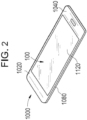
- a first aspect of this disclosure pertains to an electronic device including an embodiment of the enclosures described herein, and is illustrated in Figures 1-2 .
- the electronic device 1000 includes an enclosure 1020 having a front surface 1040, a back surface 1060, and side surfaces 1080; and electrical components (not shown) that are at least partially inside or entirely within the enclosure.
- the electronic components include at least a controller, a memory, and a display 1120, which may be at or adjacent to the front surface of the enclosure.
- the display 1120 may be present on the side surfaces 1080 and/or the back surface 1060.
- a cover glass 100 is disposed over the display 1120.
- the enclosure includes a substrate including a tactile surface, as will be described herein.
- the terms “enclosure” maybe used interchangeably with “housing” and "protective cover”.
- the enclosure 100 may include a substrate 101, which forms the entirety of the enclosure.
- the substrate may form a portion of the enclosure.
- the substrate includes opposing major surfaces, 110, 120 and opposing minor surfaces 130, 140, though other configurations are possible.
- the enclosure covers non-display areas or components of an electronic device. Such enclosures can form a back surface of an electronic device and/or any of the edges of the electronic device.
- one major surface 120 of the substrate may form an exterior surface of the electronic device and the other major surface 110 may form an interior surface of the enclosure and is adjacent to internal components of the electronic device.
- the major surface 110 forming the interior surface may include a coating forming a decorative feature, which may include a coating imparting a color, graphic, metallized surface and the like.
- only one or both the major surfaces may include the tactile surface described herein.
- all of the surfaces 110, 120, 130, 140
- the tactile surface may be present on only the major surface that forms the exterior surface of the enclosure.
- the term "anti-fingerprint” generally relates to a reduction in the visibility of fingerprints on a surface. Such reduction may be achieved by imparting hydrophobicity (i.e., contact angle of water > 90°) to a surface, oleophilicity (i.e., contact angle of oil ⁇ 90°) to a surface, and resistance to adherence of particulate or liquid matter found in fingerprints to a surface, or a combination thereof.
- the reduction may be achieved by reducing the COF of the surface.
- these properties may be imparted to a surface by various surface modifications, coatings or a combination thereof.
- the substrate may be sheet-like in form or may be shaped to have a 2.5-dimensional (as shown in Figure 3) or 3 -dimensional shape.
- the substrate is an amorphous substrate
- the amorphous substrate may include a glass substrate, which may be strengthened or non-strengthened.
- suitable glass substrates include soda lime glass substrates, alkali aluminosilicate glass substrates, alkali containing borosilicate glass substrates and alkali aluminoborosilicate glass substrates.
- the glass substrates may be free of lithia.
- the substrate may be substantially planar, although other embodiments may utilize a curved or otherwise shaped or sculpted substrate (e.g., having a 2.5-dimensional or 3-dimensional shape).
- the substrate may be substantially optically clear, transparent and free from light scattering.
- the substrate may have a refractive index in the range from about 1.45 to about 1.55. As used herein, the refractive index values are with respect to a wavelength of 550 nm.
- the substrate may be characterized as having a high average flexural strength (when compared to substrates that are not strengthened, as described herein) or high surface strain-to-failure (when compared to substrates that are not strengthened, as described herein) as measured on one or more major opposing surfaces of such substrates.
- the substrate may exhibit a color or may be a colored substrate (i.e., a substrate that appears to have a color or shade.
- the glass-based substrate may include a composition with a colorant such as oxides of cobalt, vanadium, copper, iron, manganese and the like.
- the thickness of the substrate may vary along one or more of its dimensions for aesthetic and/or functional reasons.
- the edges of the substrate may be thicker as compared to more central regions of the substrate.
- the length, width and thickness dimensions of the substrate may also vary according to the enclosure application or use.
- the substrate may be provided using a variety of different processes.
- exemplary glass substrate forming methods include float glass processes and down-draw processes such as fusion draw and slot draw.
- a glass substrate prepared by a float glass process may be characterized by smooth surfaces and uniform thickness is made by floating molten glass on a bed of molten metal, typically tin.
- molten glass that is fed onto the surface of the molten tin bed forms a floating glass ribbon.
- the temperature is gradually decreased until the glass ribbon solidifies into a solid glass substrate that can be lifted from the tin onto rollers. Once off the bath, the glass substrate can be cooled further and annealed to reduce internal stress.
- Down-draw processes produce glass substrates having a uniform thickness that possess relatively pristine surfaces. Because the average flexural strength of the glass substrate is controlled by the amount and size of surface flaws, a pristine surface that has had minimal contact has a higher initial strength. When this high strength glass substrate is then further strengthened (e.g., chemically), the resultant strength can be higher than that of a glass substrate with a surface that has been lapped and polished. Down-drawn glass substrates may be drawn to a thickness of less than about 2 mm. In addition, down drawn glass substrates have a very flat, smooth surface that can be used in its final application without costly grinding and polishing.
- the fusion draw process for example, uses a drawing tank that has a channel for accepting molten glass raw material.
- the channel has weirs that are open at the top along the length of the channel on both sides of the channel.
- the molten glass overflows the weirs. Due to gravity, the molten glass flows down the outside surfaces of the drawing tank as two flowing glass films. These outside surfaces of the drawing tank extend down and inwardly so that they join at an edge below the drawing tank.
- the two flowing glass films join at this edge to fuse and form a single flowing glass substrate.
- the fusion draw method offers the advantage that, because the two glass films flowing over the channel fuse together, neither of the outside surfaces of the resulting glass substrate comes in contact with any part of the apparatus. Thus, the surface properties of the fusion drawn glass substrate are not affected by such contact.
- the slot draw process is distinct from the fusion draw method.
- the molten raw material glass is provided to a drawing tank.
- the bottom of the drawing tank has an open slot with a nozzle that extends the length of the slot.
- the molten glass flows through the slot/nozzle and is drawn downward as a continuous substrate and into an annealing region.
- compositions used for the glass substrate may be batched with 0-2 mol. % of at least one fining agent selected from a group that includes Na 2 SO 4 , NaCl, NaF, NaBr, K 2 SO 4 , KCl, KF, KBr, and SnO 2 .
- a glass substrate may be strengthened to form a strengthened glass substrate.
- the term "strengthened substrate” refers to a glass substrate that has been chemically strengthened, for example through ion-exchange of larger ions for smaller ions in the surface of the glass or glass ceramic substrate.
- other strengthening methods known in the art such as thermal tempering, may be utilized to form strengthened glass substrates.
- the strengthened substrates described herein may be chemically strengthened by an ion exchange process.
- ions at or near the surface(s) of the glass or glass ceramic substrate are exchanged for larger metal ions from the salt bath.
- the temperature of the molten salt bath is about 400-430°C and the predetermined time period is about four to about eight hours.
- the incorporation of the larger ions into the glass substrate strengthens the substrate by creating a compressive stress in a near surface region or in regions at and adjacent to the surface(s) of the substrate.
- a corresponding tensile stress is induced within a central region or regions at a distance from the surface(s) of the substrate to balance the compressive stress.
- Glass substrates utilizing this strengthening process may be described more specifically as chemically-strengthened or ion-exchanged glass substrates.
- sodium ions in a strengthened glass substrate are replaced by potassium ions from the molten bath, such as a potassium nitrate salt bath, though other alkali metal ions having larger atomic radii, such as rubidium or cesium, can replace smaller alkali metal ions in the glass. According to particular embodiments, smaller alkali metal ions in the glass or glass ceramic can be replaced by Ag+ ions. Similarly, other alkali metal salts such as, but not limited to, sulfates, phosphates, halides, and the like may be used in the ion exchange process.
- the replacement of smaller ions by larger ions at a temperature below that at which the glass network can relax produces a distribution of ions across the surface(s) of the strengthened substrate that results in a stress profile.
- the larger volume of the incoming ion produces a compressive stress (CS) on the surface and tension (central tension, or CT) in the center of the strengthened substrate.
- CS compressive stress
- CT central tension, or CT
- Depth of exchange may be described as the depth within the strengthened glass substrate (i.e., the distance from a surface of the glass substrate to a central region of the glass or glass ceramic substrate), at which ion exchange facilitated by the ion exchange process takes place.
- Maximum CT values are measured using a scattered light polariscope (SCALP) technique as known in the art.
- SCALP scattered light polariscope
- Compressive stress is measured by surface stress meter (FSM) using commercially available instruments such as the FSM-6000, manufactured by Orihara Industrial Co., Ltd. (Japan).
- FSM surface stress meter
- FSM-6000 manufactured by Orihara Industrial Co., Ltd. (Japan).
- SOC stress optical coefficient
- ASTM standard C770-16 entitled "Standard Test Method for Measurement of Glass Stress-Optical Coefficient”.
- DOC means the depth at which the stress in the chemically strengthened alkali aluminosilicate glass article described herein changes from compressive to tensile.
- DOC may be measured by FSM or SCALP depending on the ion exchange treatment. Where the stress in the glass article is generated by exchanging potassium ions into the glass article, FSM is used to measure DOC. Where the stress is generated by exchanging sodium ions into the glass article, SCALP is used to measure DOC.
- the DOC is measured by SCALP, since it is believed the exchange depth of sodium indicates the DOC and the exchange depth of potassium ions indicates a change in the magnitude of the compressive stress (but not the change in stress from compressive to tensile); the exchange depth of potassium ions in such glass articles is measured by FSM.
- a strengthened glass substrate can have a surface compressive stress of 300 MPa or greater, e.g., 400 MPa or greater, 450 MPa or greater, 500 MPa or greater, 550 MPa or greater, 600 MPa or greater, 650 MPa or greater, 700 MPa or greater, 750 MPa or greater or 800 MPa or greater.
- the strengthened glass substrate may have a compressive depth of layer 15 ⁇ m or greater, 20 ⁇ m or greater (e.g., 25 ⁇ m, 30 ⁇ m, 35 ⁇ m, 40 ⁇ m, 45 ⁇ m, 50 ⁇ m or greater) and/or a central tension of 10 MPa or greater, 20 MPa or greater, 30 MPa or greater, 40 MPa or greater (e.g., 42 MPa, 45 MPa, or 50 MPa or greater) but less than 100 MPa (e.g., 95, 90, 85, 80, 75, 70, 65, 60, 55 MPa or less).
- the strengthened glass substrate has one or more of the following: a surface compressive stress greater than 500 MPa, a depth of compressive layer greater than 15 ⁇ m, and a central tension greater than 18 MPa.
- strengthened glass substrates with a surface compressive stress greater than 500 MPa and a compressive depth of layer greater than about 15 ⁇ m typically have greater strain-to-failure than non-strengthened glass substrates (or, in other words, glass substrates that have not been ion exchanged or otherwise strengthened).
- Example glasses that may be used in the substrate may include alkali aluminosilicate glass compositions or alkali aluminoborosilicate glass compositions, though other glass compositions are contemplated. Such glass compositions may be characterized as ion exchangeable. As used herein, "ion exchangeable" means that a substrate comprising the composition is capable of exchanging cations located at or near the surface of the substrate with cations of the same valence that are either larger or smaller in size.
- One example glass composition comprises SiO 2 , B 2 O 3 and Na 2 O, where (SiO 2 + B 2 O 3 ) ⁇ 66 mol. %, and Na 2 O ⁇ 9 mol. %.
- the glass composition includes at least 6 wt.% aluminum oxide.
- the substrate includes a glass composition with one or more alkaline earth oxides, such that a content of alkaline earth oxides is at least 5 wt.%. Suitable glass compositions, in some embodiments, further comprise at least one of K 2 O, MgO, and CaO.
- the glass compositions used in the substrate can comprise 61-75 mol.% SiO2; 7-15 mol.% Al 2 O 3 ; 0-12 mol.% B 2 O 3 ; 9-21 mol.% Na 2 O; 0-4 mol.% K 2 O; 0-7 mol.% MgO; and 0-3 mol.% CaO.
- a further example glass composition suitable for the substrate comprises: 60-70 mol.% SiO 2 ; 6-14 mol.% Al 2 O 3 ; 0-15 mol.% B 2 O 3 ; 0-15 mol.% Li 2 O; 0-20 mol.% Na 2 O; 0-10 mol.% K 2 O; 0-8 mol.% MgO; 0-10 mol.% CaO; 0-5 mol.% ZrO 2 ; 0-1 mol.% SnO 2 ; 0-1 mol.% CeO 2 ; less than 50 ppm As 2 O 3 ; and less than 50 ppm Sb 2 O 3 ; where 12 mol.% ⁇ (Li 2 O + Na 2 O + K 2 O) ⁇ 20 mol.% and 0 mol.% ⁇ (MgO + CaO) ⁇ 10 mol.%.
- a still further example glass composition suitable for the substrate comprises: 63.5-66.5 mol.% SiO 2 ; 8-12 mol.% Al 2 O 3 ; 0-3 mol.% B 2 O 3 ; 0-5 mol.% Li 2 O; 8-18 mol.% Na 2 O; 0-5 mol.% K 2 O; 1-7 mol.% MgO; 0-2.5 mol.% CaO; 0-3 mol.% ZrO 2 ; 0.05-0.25 mol.% SnO 2 ; 0.05-0.5 mol.% CeO 2 ; less than 50 ppm As 2 O 3 ; and less than 50 ppm Sb 2 O 3 ; where 14 mol.% ⁇ (Li 2 O + Na 2 O + K 2 O) ⁇ 18 mol.% and 2 mol.% ⁇ (MgO + CaO) ⁇ 7 mol.%.
- an alkali aluminosilicate glass composition suitable for the substrate comprises alumina, at least one alkali metal and, in some embodiments, greater than 50 mol.% SiO 2 , in other embodiments at least 58 mol.% SiO 2 , and in still other embodiments at least 60 mol.% SiO 2 , wherein the ratio ((Al 2 O 3 + B 2 O 3 )/ ⁇ modifiers)>1, where in the ratio the components are expressed in mol.% and the modifiers are alkali metal oxides.
- This glass composition in particular embodiments, comprises: 58-72 mol.% SiO 2 ; 9-17 mol.% Al 2 O 3 ; 2-12 mol.% B 2 O 3 ; 8-16 mol.% Na 2 O; and 0-4 mol.% K 2 O, wherein the ratio((Al 2 O 3 + B 2 O 3 )/ ⁇ modifiers)>1.
- the substrate may include an alkali aluminosilicate glass composition comprising: 64-68 mol.% SiO 2 ; 12-16 mol.% Na 2 O; 8-12 mol.% Al 2 O 3 ; 0-3 mol.% B 2 O 3 ; 2-5 mol.% K 2 O; 4-6 mol.% MgO; and 0-5 mol.% CaO, wherein: 66 mol.% ⁇ SiO 2 + B 2 O 3 + CaO ⁇ 69 mol.%; Na 2 O + K 2 O + B 2 O 3 + MgO + CaO + SrO > 10 mol.%; 5 mol.% ⁇ MgO + CaO + SrO ⁇ 8 mol.%; (Na 2 O + B 2 O 3 ) - Al 2 O 3 ⁇ 2 mol.%; 2 mol.% ⁇ Na 2 O - Al 2 O 3 ⁇ 6 mol.%; and 4 mol.% ⁇ (Na 2 O + K 2 ; 64-
- the substrate may comprise an alkali aluminosilicate glass composition comprising: 2 mol% or more of Al 2 O 3 and/or ZrO 2 , or 4 mol% or more of Al 2 O 3 and/or ZrO 2 .
- the substrate according to one or more embodiments can have a thickness in the range from about 100 ⁇ m to about 5 mm.
- Example substrate thicknesses range from about 100 ⁇ m to about 500 ⁇ m (e.g., 100, 200, 300, 400 or 500 ⁇ m). Further example substrate thicknesses range from about 500 ⁇ m to about 1000 ⁇ m (e.g., 500, 600, 700, 800, 900 or 1000 ⁇ m).
- the substrate may have a thickness greater than about 1 mm (e.g., about 2, 3, 4, or 5 mm). In one or more specific embodiments, the substrate may have a thickness of 2 mm or less or less than 1 mm.
- the substrate may be acid polished or otherwise treated to remove or reduce the effect of surface flaws.
- substrate 101 comprises a tactile surface.
- the tactile surface may comprise at least a portion of one or both major surfaces 110, 120 of the substrate 101 or one or more minor surfaces 130, 140 of the substrate.
- the tactile surface may be formed on at least a portion of one, two, three or all of the surfaces of the substrate. In some instances, the tactile surface may be formed on all of one or more surfaces of the substrate 101.
- the tactile surface 150 is formed on major surface 120.
- the tactile surface may be formed in a predetermined design.
- the enclosure may include a design occupying a portion of a surface, and the tactile surface may be formed on the surface to cover or be disposed adjacent to the design. The design on the enclosure may be provided by a film disposed on one major surface of the substrate and the tactile surface may be formed on the opposite major surface, having the same shape as the design.
- the tactile surface may include a textured surface (or surface that has been modified to include a texture), a coating, or a combination thereof (i.e., a coated textured surface).
- the substrate may exhibit certain properties as measured on the tactile surface.
- the substrate may exhibit a haze as measured at the tactile surface in the range from about 60% to about 120%, from about 65% to about 120%, from about 70% to about 120%, from about 75% to about 120%, from about 80% to about 120%, from about 90% to about 120%, from about 100% to about 120%, from about 100% to about 110%, from about 60% to about 110%, from about 60% to about 100%, from about 60% to about 90%, from about 60% to about 80%, or from about 60% to about 70%,
- the substrate may exhibit a transmittance haze as measured through the tactile surface of about 60% or greater, about 70% or greater, about 80% or greater, about 90% or greater, or about 95% or greater.
- the transmittance haze may be up to about 100%.
- the substrate may exhibit a transmittance haze as measured through the tactile surface in the range from about 60% to about 100%, from about 65% to about 100%, from about 70% to about 100%, from about 75% to about 100%, from about 80% to about 100%, from about 90% to about 100%, from about 92% to about 100%, from about 93% to about 94%, from about 95% to about 100%, from about 96% to about 100%, from about 97% to about 100%, from about 98% to about 100%, from about 99% to about 100%, from about 60% to about 98%, from about 60% to about 96%, from about 60% to about 95%, from about 60% to about 94%, from about 60% to about 92%, from about 60% to about 90%, from about 60% to about 85%, or from about 60% to about 80%.
- the substrate may exhibit a reflectance haze (as measured on the tactile surface) of about 60% or greater, about 70% or greater, about 80% or greater or about 90% or greater. In some instances, the reflectance haze may be up to about 100%.
- the substrate may exhibit a reflectance haze as measured on the tactile surface in the range from about 60% to about 100%, from about 65% to about 100%, from about 70% to about 100%, from about 75% to about 100%, from about 80% to about 100%, from about 90% to about 100%, from about 92% to about 100%, from about 93% to about 94%, from about 95% to about 100%, from about 96% to about 100%, from about 97% to about 100%, from about 98% to about 100%, from about 99% to about 100%, from about 60% to about 98%, from about 60% to about 96%, from about 60% to about 95%, from about 60% to about 94%, from about 60% to about 92%, from about 60% to about 90%, from about 60% to about 85%, or from about 60% to about 80%.
- Reflectance haze may be measured at 2 degrees from specular or 5 degrees from specular. In some embodiments, haze may be measured according to ASTM E430 using a transparency meter such as the Haze-Gard meter supplied by BYK-Gardner GmbH, of Geretsried, Germany.
- the transmittance haze described herein may be influenced by whether the textures tactile surface is present on a single major surface or both major surfaces.
- Figure 4 shows the correlation of transmittance haze of the substrate including a tactile surface only a single surface (typically a single major surface) or on opposing surfaces (typically, opposing major surfaces), based on Examples 1 and 2.
- the substrate may exhibit a 20° distinctness of image (DOI) (as measured on the tactile surface) of about 90 or less (e.g., about 85 or less, about 80 or less, about 60 or less, or about 40 or less).
- DOI 20° distinctness of image
- distinctness of image is defined by method A of ASTM procedure D5767 (ASTM 5767), entitled “Standard Test Methods for Instrumental Measurements of Distinctness-of-Image Gloss of Coating Surfaces”.
- ASTM 5767 ASTM procedure D5767
- substrate reflectance factor measurements are made on the anti-glare surface at the specular viewing angle and at an angle slightly off the specular viewing angle. The values obtained from these measurements are combined to provide a DOI value.
- DOI 1 ⁇ Ros Rs ⁇ 100 , where Ros is the relative reflection intensity average between 0.2° and 0.4 away from the specular reflection direction, and Rs is the relative reflection intensity average in the specular direction (between +0.05° and -0.05°, centered around the specular reflection direction).
- the input light source angle is +20° from the sample surface normal (as it is throughout this disclosure), and the surface normal to the sample is taken as 0°, then the measurement of specular reflected light Rs is taken as an average in the range of about -19.95° to -20.05°, and Ros is taken as the average reflected intensity in the range of about -20.2° to -20.4° (or from - 19.6° to -19.8°, or an average of both of these two ranges).
- DOI values should be directly interpreted as specifying a target ratio of Ros/Rs as defined herein.
- the anti-glare surface has a reflected scattering profile such that > 95% of the reflected optical power is contained within a cone of +/- 10°, where the cone is centered around the specular reflection direction for any input angle.
- the substrate may exhibit a gloss at 60° of 70% or less (e.g., 65% or less, 50% or less, 40% or less, 30% or less or 20% or less), as measured on the tactile surface.
- the DOI and gloss is measured on the tactile surface in reflected mode (i.e., without taking into account the other surfaces of the substrate). Transmission haze performance is in terms of the entire substrate, since these values are measured in the transmitted mode.
- the textured surface may include a plurality of features disposed on the surface that are light-scattering, create a roughness or a combination thereof.
- the features may be disposed directly on the surface or indirectly on the surface in a random or non-random manner. Randomly disposed features may provide a smooth touch-feeling when the surface is contacted or swiped with a finger or skin.
- features imparting a degree of roughness can create a smooth touch-feeling that facilitates gliding of fingers or other objects over the surface by limiting the contact area of the finger or object with the textured surface.
- the plurality of features may exhibit a longest cross-sectional dimension (i.e., the largest feature may have a longest cross-sectional dimension) in the range from about 5 micrometers to about 100 micrometers. Such dimensions may be found in a sample surface section having dimensions of about 0.5 mm by 0.5mm to capture a representative average including a number of typical surface features in the range from about 10 to about 1000.
- the features may have a longest cross-sectional dimension in the range from about 5 micrometers to about 90 micrometers, from about 5 micrometers to about 80 micrometers, from about 5 micrometers to about 70 micrometers, from about 5 micrometers to about 60 micrometers, from about 5 micrometers to about 50 micrometers, from about 5 micrometers to about 40 micrometers, from about 5 micrometers to about 30 micrometers, from about 10 micrometers to about 100 micrometers, from about 15 micrometers to about 100 micrometers, from about 20 micrometers to about 100 micrometers, from about 30 micrometers to about 100 micrometers, or from about 10 micrometers to about 50 micrometers.
- the features may include an average longest cross-sectional dimension that is about 2 times or more than the longest cross-sectional dimension of any one feature.
- the features may include an average longest cross-sectional dimension that is about 2 times or less than the longest cross-sectional dimension of any one feature.
- the longest cross-sectional dimension of the features may be evaluated by optical microscope under 200x magnification. To determine the average longest cross-sectional dimension of the features, ten of the largest features are selected over a sample surface section having dimensions of about 0.5 mm by 0.5mm, and measured by optical microscope. The average measurement is reported as the average longest cross-sectional dimension of the selected features.
- the textured surface may exhibit a RMS roughness height (i.e., in the z-direction) in the range from about 0.02 micrometers to about 10 micrometers, from about 0.02 micrometers to about 8 micrometers, from about 0.02 micrometers to about 6 micrometers, from about 0.02 micrometers to about 4 micrometers, from about 0.05 micrometers to about 2 micrometers, from about 0.05 micrometers to about 1 micrometer, or from about 0.1 to about 0.8 micrometers.
- the RMS roughness height is measured using methods known in the art such as atomic force microscopy (AFM), stylus contact profilometry, and optical interference profilometry.
- AFM atomic force microscopy
- stylus contact profilometry stylus contact profilometry
- optical interference profilometry optical interference profilometry
- the textured surface may exhibit a surface roughness Ra measuring the vertical height of the features (e.g., as measured in the z-direction by an optical surface profiler, such as the 3D Optical Surface Profiler available from Zygo Corporation) in the range from about 500 nm or greater.
- Ra measuring the vertical height of the features (e.g., as measured in the z-direction by an optical surface profiler, such as the 3D Optical Surface Profiler available from Zygo Corporation) in the range from about 500 nm or greater.
- the surface Ra may be in the range from about 500 nm to about 2000 nm, from about 500 nm to about 1800 nm, from about 500 nm to about 1600 nm, from about 500 nm to about 1500 nm, from about 500 nm to about 1400 nm, from about 500 nm to about 1200 nm, from about 500 nm to about 1000 nm, from about 600 nm to about 2000 nm, from about 800 nm to about 2000 nm, from about 900 nm to about 2000 nm, from about 1000 nm to about 2000 nm, from about 1100 nm to about 2000 nm, from about 1200 nm to about 2000 nm, or from about 900 nm to about 1300 nm.
- the surface Ra roughness as described herein is measured over a sample surface section having dimensions of about 0.5 mm by 0.5mm.
- the textured surface may include a low frequency of features, large sized features, or a combination thereof which cause fingerprint oils to collect in between the features (i.e., in the valleys created between the features) of the textured structure. Collection of oils between the features reducing the fraction of the surface that is covered with oil droplets, thus reducing light scattering from the fingerprint oils.
- the textured surface may have an RMS roughness height in the range from about 0.05 micrometers to about 1 micrometer over a samples size having dimensions of about 0.5 mm by 0.5mm.
- the textured surface may have a RMS roughness height that is large enough to significantly reduce transfer of fingerprint oils into the valleys of the structure, thus also reducing light scattering through limiting the fraction of the surface that is covered with oil droplets.
- Such textured surfaces may have a RMS roughness height in the range from about 1 micrometer to about 10 micrometers over a samples size having dimensions of about 0.5 mm by 0.5mm.
- the textured surface comprises a lateral spatial period (i.e., in the x-y in-plane direction) in the range from about 0.1 micrometers to about 500 microns, from about 0.1 micrometers to about 400 microns, from about 0.1 micrometers to about 300 microns, from about 0.1 micrometers to about 200 microns, from about 0.1 micrometers to about 100 microns, from about 0.1 micrometers to about 50 microns, from about 0.1 micrometers to about 10 microns, from about 0.5 micrometers to about 500 microns, from about 1 micrometer to about 500 microns, from about 10 micrometers to about 500 microns, from about 50 micrometers to about 500 microns, from about 100 micrometers to about 500 microns, from about 1 micrometer to about 100 micrometers, or from about 10 micrometers to about 50 micrometers.
- Such lateral special period ranges are measured over a samples size having dimensions of about 1 mm by 1 mm.
- roughness parameters and surface profiles can be measured using known techniques such as atomic force microscopy (AFM), stylus contact surface profilometry, or optical interference surface profiling.
- AFM atomic force microscopy
- stylus contact surface profilometry stylus contact surface profilometry
- optical interference surface profiling optical interference surface profiling
- the textured surface may be formed by a variety of methods such as wet etching, dry etching, masking and etching, photolithography, and the like.
- the textured surface may be formed by chemical etching at least one surface of the substrate. Chemical etching may include applying a mask on selected portions of the surface and removing the exposed portions of the surface by etching sand blasting or grinding.
- the mask may be formed by forming precipitates on the surface.
- the masking may be achieved by polymer masking, polymer particle masking, or ink-jetting a mask, or may utilize a mask formed by photolithography or nanoimprint lithography, a phase-separating polymer mask, a soluble (organic or inorganic) phase embedded in an insoluble polymer mask, an insoluble polymer mask including particles embedded therein or a combination thereof.
- the etchants may comprise hydrofluoric acid or hydroxide material such as KOH or NaOH plus chelating agents.
- Hydrofluoric acid may be combined with other acids such as hydrocholoric, sulfuric, acetic, or nitric acids, where minimizing the formation of precipitate formation is desired and/or where etching the surface of the substrate without changing the resulting surface composition is desired.
- enclosures with a textured surface may be formed into different shapes through polishing or hot-forming, which may be performed either before or after the texturing process.
- an enclosure with a textured surface may be strengthened (as described below) after the textured surface is formed.
- the textured surface may be formed by adding features to the surface of the substrate (especially in the case of organic substrates).
- the features may include particles that are attached or bonded to the surface.
- an adhesive may be utilized to bond the particles to the surface.
- the particles may be directly bonded to the surface.
- the particles may have an average major dimension in the range from 5 micrometers to about 100 micrometers.
- the particles may be formed from the same material as the substrate, or from a different material.
- the textured surface may include a coating or coatings disposed on the textured surface, forming a coated textured surface.
- the coatings may be placed on top of the textured surface to provide various functionalities.
- the coatings may include ink coatings, hard coatings, scratch-resistant coatings, low-friction coatings, high-friction coatings, oleophobic coatings, oleophilic coatings, hydrophobic coatings, hydrophilic coatings, coatings that exhibit hydrophobicity and oleophobicity, reflective or anti-reflective coatings, or easy-to-clean coatings that show a combination of these functions.
- the specific choice of coating depends on the desired uses of the electronic device, as well as design considerations.
- the coatings may be relatively thick (e.g., in the range from about 1 micrometer to about 3 micrometers, in the case of scratch-resistant coatings), or may be relatively thin (e.g., in the range from about 0.5 nanometers to about 50 nanometers, in the case of hydrophobicity and oleophobicity coatings, oleophobic coatings or oleophilic coatings).
- the textured surface imparts oleophilicity or hydrophobicity and oleophobicity to the substrate surface (without a coating disposed thereon) and thus forms a tactile surface that exhibits anti-fingerprint properties or performance.
- the textured surface enhances or promotes the oleophilicity or hydrophobicity and oleophobicity of certain substrate, such as glass. Without being bound by theory, it is believed that this enhanced oleophilicity or hydrophobicity and oleophobicity provides anti-fingerprint functionality because the visibility of a fingerprint on a surface is largely determined by light scattering, and in turn this light scattering is largely dependent on the size of the scattering oil droplets left behind by a fingerprint.
- Oleophobic surfaces or hydrophobic and oleophobic surfaces tend to create a large number of fingerprint droplets having an average longest cross-sectional dimension of 2 micrometers or less, as measured by optical or other known means for measuring such droplets. Such droplets are highly light scattering droplets and thus increase the visibility of the fingerprint.
- oleophilic surfaces tend to create smears or very broad droplets that are larger than 5 micrometers in size, with much reduced light scattering, particularly at scattering angles greater than about 5 degrees away from the specular reflection angle. Accordingly, it is believed a textured surface exhibiting oleophilicity provides improved anti-fingerprint performance.
- the textured surface includes a coating.
- the coating is a low-friction coating or a coating that reduces COF of the textured surface.
- the coating is also at least somewhat oleophilic, to form an oleophilic coated textured surface or a hydrophobic and oleophobic coated textured surface.
- Such coated textured surfaces can provide a smooth gliding surface for fingers.
- such coated textured surfaces can provide some spreading of oil droplets to further minimize light scattering.
- coated textured surfaces including a low-friction coating exhibit a kinetic coefficient of friction (COF) of less than 0.3, when measured by the COF Test Method (described herein).
- coated textured surfaces including a low-friction coating exhibit a static COF of less than 0.3, as measured by the COF Test Method.
- low-friction coatings may include glass surface reactive porous alkyl siloxanes (e.g., methyl siloxane, ethyl siloxane, propyl siloxane, and the like), porous phenyl siloxanes, porous alkyl silanes, inorganic coatings (such as alumina, titania, zirconia, aluminum titanium nitride) or combinations thereof.
- the textured surface may include a high-friction coating forming a coated textured surface.
- high-friction coatings examples include alkyl siloxanes (e.g., methyl siloxane, ethyl siloxane, propyl siloxane, and the like), phenyl siloxanes, alkyl silanes and other similar materials.
- the COF Test Method is used to measure static and kinetic COF using a coefficient of friction instrument (COF-1000) supplied by ChemInstruments, Inc. of Fairfield, Ohio, coupled with data management software. Measurements were obtained using a 200 g or 500 g load applied at 12inches/minute. Unless specified otherwise, the samples measured had dimensions of 65 mm by 135 mm, and were attached to the moving substrate by means of a clip.
- the test material included a microfiber cloth supplied by Photodon, LLC of Traverse City, Michigan under the trade name 382ZZ and having zigzag edges with dimensions 7 inches by 6 inches. The cloth comprises 80% polyester, 20% nylon and has a density of 260 grams/m 2 .
- Cloth was cut into squares having dimensions of 2 inches by 2 inches and affixed to a test glass substrate by double sided tape.
- the test apparatus is illustrated in Figure 5 , which shows the substrate 212 (with the tactile surface) be tested affixed to a moving substrate 210.
- the cloth 222 is shown affixed to a test glass substrate 220.
- the cloth 222 and test glass substrate 220 are coupled to the coefficient of friction instrument 300.
- the tactile surface faces the cloth 222 so the COF of the surface can be measured.
- the tactile surface is substantially free of a coating (e.g., free of an oleophilic coating) and may exhibit a static or kinetic COF of less than 0.5, when measured under the COF Test Method using a load of 500g.
- the tactile surface is substantially free of a coating (e.g., free of an oleophilic coating) and may exhibit a static or kinetic COF of in the range from about 0.05 to about 0.4, 0.05 to about 0.3, 0.05 to about 0.2, 0.1 to less than 0.5, 0.15 to less than 0.5, or 0.2 to less than 0.5.
- the tactile surface may include a low-friction coating and exhibits the static or kinetic COF disclosed herein.
- a bare tactile surface exhibits an oleophilicity that decreases with use, as oils, dirt and fingerprints accumulate on the textured surface.
- the textured surface includes a coating that maintains a certain degree of oleophilicity.
- Such coatings can include TiO 2 , which is believed to be a "self-cleaning" material after exposure to ultraviolet light. Specifically, TiO 2 coatings can chemically break down absorbed oils and dirt after exposure to ultraviolet light or even sunlight through photocatalysis.
- Enclosures according to one or more embodiments may be free of a textured surface but include a coating forming the anti-fingerprint surface. Such coatings impart oleophilicity or hydrophobicity and oleophobicity to the surface.
- the tactile surface exhibits an anti-fingerprint functionality such that, after a wipe of a finger or other applicator containing oil or oleic acid, the surface includes droplets that have an average major dimension of greater than about 2 micrometers, greater than about 5 micrometers, or greater than about 10 micrometers.
- the visibility, based on brightness, may be calculated by the following equation, where the subscript 1 indicates an area including a fingerprint and subscript 2 indicates an area without a fingerprint: the absolute value of the difference (brightness 1 - brightness 2 ), divided by the sum (brightness 1 + brightness 2 ).
- the texture surface exhibits a visibility of less than about 0.99, less than about 0.95, less than about 0.8, less than about 0.7, less than about 0.6, less than 0.5, less than 0.25, less than 0.2, less than 0.1, less than 0.05 at certain selected angles.
- the enclosure may be transparent, translucent, or opaque.
- such enclosures may exhibit an average total transmittance (taking into account both the interior and exterior surface of the enclosure of about 80% or greater, 85% or greater, 90% or greater, or 95% or greater, over the visible spectrum.
- the enclosure may exhibit an average total transmittance in the range from about 80% to about 96%, from about 80% to about 94%, or from about 80% to about 92%, over the visible spectrum.
- the term "transmittance” is defined as the percentage of incident optical power within a given wavelength range transmitted through a material (e.g., the enclosure or portions thereof). Transmittance is measured using a specific line width. In one or more embodiments, the spectral resolution of the characterization of the transmittance is less than 5 nm or 0.02 eV.
- the "visible spectrum” includes the wavelength range from about 420 nm to about 700 nm.
- the enclosure also exhibits 4-point bend strength, stiffness or Young's Modulus, hardness, crack indentation threshold, thermal conductivity, and strength (in terms of depth of compressive layer (DOC), surface compressive stress and central tension).
- DOC depth of compressive layer
- the enclosure may include the substrate described herein.
- the substrate may form the entire enclosure or a portion of the enclosure.
- the enclosure permits transmission of wireless data transmission or wireless charging energy.
- the enclosure exhibits both radio and microwave frequency transparency, as defined by a loss tangent of less than 0.03 and at a frequency range of between 15 MHz to 3.0 GHz.
- the article, particularly the electronic device enclosure exhibits radio and microwave frequency transparency, as defined by a loss tangent of less than 0.015 over the frequency range of between 500 MHz to 3.0 GHz.
- This radio and microwave frequency transparency feature is especially important for wireless hand held devices that include antennas internal to the enclosure. This radio and microwave transparency allows the wireless signals to pass through the enclosure and in some cases enhances these transmissions.
- the enclosure is permits transmission of magnetic fields and/or inductive fields.
- the enclosure may also exhibit various mechanical attributes for use with portable electronic devices.
- some embodiments of the enclosure exhibit any one or more of a fracture toughness of greater than 0.6 MPa ⁇ m 1 ⁇ 2 , a 4-point bend strength of greater than 350 MPa, a Vickers hardness of at least 600 kgf/mm 2 and a Vickers median/radial crack initiation threshold of at least 5 kgf, a Young's Modulus in the range from about 50 GPa to about 100 GPa, a thermal conductivity of less than 2.0 W/m°C.
- the enclosure exhibits a combination of fracture toughness in excess of 0.6 MPa ⁇ m 1 ⁇ 2 , the above-recited Vickers hardness/indentation threshold, and 4-point bend strength.
- the enclosure exhibits a fracture toughness of greater than 0.70 MPa ⁇ m1 ⁇ 2, and an 4-point bend strength of greater than 475 MPa or greater than 525 MPa and a Young's Modulus in the range from about 50 GPa to about 75 GPa.
- the enclosure described herein may deform upon indentation primarily by densification rather than by shear faulting.
- the enclosure is free of subsurface faulting and radial cracks upon deformation.
- the resulting enclosure is more resistant to crack initiation by shear faulting.
- the enclosure comprises a strengthened substrate and exhibits a Vickers median/radial crack initiation threshold of at least 5 kilogram force (kgf).
- the enclosure has a Vickers median/radial crack initiation threshold of at least about 10 kgf or at least about 30 kgf.
- the enclosure exhibits a thermal conductivity of less than 2 W/m°C, and thus, remains cool to the touch even in high operating temperatures (e.g., temperatures approaching 100°C). In some embodiments, the enclosure exhibits a thermal conductivity of less than 1.5 W/m°C. For comparison, ceramics such as alumina may exhibit thermal conductivities as high as 29 W/m°C.
- Alkali aluminosilicate glass substrates having a sheet forma and which were not strengthened having a nominal composition of 57.5 mol% SiO 2 , 16.5 mol% Al 2 O 3 , 16 mol% Na 2 O, 2.8 mol% MgO and 6.5 mol% P 2 O 5 , and a thickness of 0.7 mm were cleaned by immersing in detergent solution and applying ultrasonic agitation to the detergent solution. The cleaned substrates were then removed from the detergent solution and then statically etched by applying an etchant including 6 weight percent hydrofluoric acid (HF) and 15 weight percent NH 4 F for 8 minutes (Step A). The etched substrates were then rinsed and thoroughly with DI water.
- HF hydrofluoric acid
- Example 1A-1K included textured surface on both major surfaces and both minor surfaces.
- One glass substrate was not subjected to any etching steps (Comparative Example 1L).
- the transmittance haze, transmittance, final substrate thickness, longest cross-sectional dimension of the largest feature, and surface roughness (Ra) were measured on the major surfaces of resulting Examples 1A-1K and Comparative Example IL.
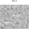
- Figure 6 shows an optical microscope image of Example 1K taken at 200x magnification.
- the largest lateral features had a longest cross-sectional dimension of about 44.452 micrometers and 47.330 micrometers (a 50 micrometer scale is included for reference).
- Alkali aluminosilicate glass substrates having a sheet forma and which were not strengthened having the same nominal composition as Example 1 and identical thicknesses were cleaned by immersing in detergent solution and applying ultrasonic agitation to the detergent solution. The cleaned substrates were then removed from the detergent solution. A single major surface was coated with an etch-resistant film and then statically etched by applying an etchant including 2 weight percent or 6 weight percent hydrofluoric acid (HF) and 15 weight percent or 30 weight percent NH 4 F for 8 minutes (Step C). The etched substrates were then rinsed and thoroughly with DI water.
- HF hydrofluoric acid
- Examples 2A-2E included a textured surface on a single major surface, and both minor surfaces. The opposing major surface was free of a textured surface.
- Table 2 Properties for Examples 2A-2E, based on etching times.
- Step B 2A 8 (3 wt% HF/30 wt% NH 4 F) 10.6 12.8 92.4 63.1 227 21 2B 8 (6 wt% HF/15 wt% NH 4 F) 16.4 33.2 1.1 22.6 583 37 2C 8 (6 wt% HF/15 wt% NH 4 F) 10 49.5 0.8 16.4 610 34 2D 8 (6 wt% HF/15 wt% NH 4 F) 8.4 61.5 1.0 14.8 760 32 2E 8 (6 wt% HF/15 wt% NH 4 F) 2 97.6 0.0 11.9 1113 n/a
- the static COF of Examples 2A-2E was measured (as described herein) before and after coating with an easy-to-clean coating, as shown in Table 3.
- the easy-to-clean coating included an alkoxysilane functional perfluoropolyether (PFPE) hybrid polymer supplied by Dow Coming Corporation of Midland, Michigan, under the trade name Dow Coming 2634, and hydrofluoroether solvent supplied by The 3M Company of Minneapolis, Minnesota, under the trade name 3M TM Novec TM 7200 Engineered Fluid.
- PFPE alkoxysilane functional perfluoropolyether
- the easy-to-clean coating was prepared by combining 4.2 mL of the alkoxysilane functional perfluoropolyether (PFPE) hybrid polymer and 1 L of the hydrofluorether solvent and sprayed using a spray applicator supplied by Nordson ASYMTEK of Carlsbad, California, under the trademark SC-300 Swirl Coat ® , using a valve supplied by Nordson EFD of East Buffalo, Rhode Island, under the trade name MM781-SYS MicroMark.
- the coating was applied using a 2.5mL/minute flow rate, at 30 psi air pressure, 20 inch /minute velocity for 2 hours in an environment at 50 °C and 50% relative humidity.
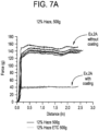
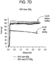
- FIGS 7A-7E show the impact of easy-to-clean (ETC) coating on coefficient of friction (COF) for the different haze and roughness levels of Examples 2A-2E.
- the COF was measured five times on the same Example using a 500 g load.
- the ETC coating was more effective in reducing the COF when the surface roughness (and haze) is low, and became less effective as surface roughness (and haze) increased.
- Figure 8 shows the static COF of Examples 2B-2E as a function of transmittance haze. The results showed that the application of an ETC coating was more effective in reducing the COF when the surface roughness (and haze) is low, and became less effective as surface roughness (and haze) increased.
- Example 3A-3D Glass substrates having the same nominal composition as Example 1 and identical shape and thickness were sandblasted at a pressure of 20 psi with SiC particles to create a textured surface exhibiting high transmittance haze and roughness. The substrates were then rinsed with DI water to remove any debris from sandblasting. The substrates where then chemically polished using a 5 weight percent HF solution for various times (as indicated in Table 4) and then rinsed in DI water again. Resulting Examples 3A-3D included a textured surface on a single major surface. The opposing major surface was free of a textured surface. The transmittance haze, and surface roughness (Ra), were measured on the textured surface of resulting Examples 3A-3D.
- Table 4 Properties for Examples 3A-3D, based on chemical polishing time. Transmittance Haze (%) Surface Roughness (nm) Chemical Polishing time in 5wt% HF (min) 90+% 1460 0 90+% 1941 2 90+% 2405 4 90+% 2367 8
Landscapes
- Chemical & Material Sciences (AREA)
- Engineering & Computer Science (AREA)
- Chemical Kinetics & Catalysis (AREA)
- Physics & Mathematics (AREA)
- General Chemical & Material Sciences (AREA)
- Geochemistry & Mineralogy (AREA)
- Materials Engineering (AREA)
- Organic Chemistry (AREA)
- Life Sciences & Earth Sciences (AREA)
- Optics & Photonics (AREA)
- General Physics & Mathematics (AREA)
- Microelectronics & Electronic Packaging (AREA)
- Mechanical Engineering (AREA)
- Ceramic Engineering (AREA)
- Surface Treatment Of Glass (AREA)
- Glass Compositions (AREA)
- Devices For Indicating Variable Information By Combining Individual Elements (AREA)
- Laminated Bodies (AREA)
Claims (11)
- Dispositif électronique comprenant : une enceinte, et des composants électriques disposés au moins partiellement à l'intérieur de l'enceinte, lesdits composants électroniques comprenant un dispositif de commande, une mémoire et un dispositif d'affichage,ladite enceinte comprenant un substrat amorphe, et ledit substrat comprenantune transmission moyenne supérieure ou égale à 80 % sur le spectre visible ;un coefficient de frottement statique inférieur à 0,3,une rugosité de surface Ra supérieure ou égale à 500 nm, etl'un ou les deux
d'un trouble de transmission supérieur à 60 %, etd'un flou spéculaire à 2 degrés par rapport à la direction spéculaire ou à 5 degrés par rapport à la direction spéculaire supérieur à 60 %. - Dispositif électronique de la revendication 1, ledit substrat comprenant l'un quelconque d'un verre sodocalcique, d'un verre d'aluminosilicate alcalin, d'un verre de borosilicate contenant des alcalis et d'un verre d'aluminoborosilicate alcalin.
- Dispositif électronique de la revendication 1 ou la revendication 2, ledit substrat étant renforcé.
- Enceinte de dispositif électronique selon l'une quelconque des revendications 1-3, ledit substrat comprenant en outre l'une quelconque ou plusieursd'une couche de surface compressive comportant une profondeur de couche (DOC) supérieure ou égale à 20 µm,d'une contrainte de compression de surface supérieure à 400 MPa, etd'une tension centrale supérieure à 20 MPa.
- Dispositif électronique selon l'une quelconque des revendications précédentes, ledit substrat comprenant une couche d'encre disposée sur une surface principale du substrat.
- Dispositif électronique selon l'une quelconque des revendications précédentes, ledit substrat comprenant un verre coloré.
- Dispositif électronique selon l'une quelconque des revendications précédentes, ledit trouble de transmission étant supérieur à 90 %.
- Dispositif électronique selon l'une quelconque des revendications précédentes, ledit flou spéculaire soit à 2 degrés par rapport à la direction spéculaire soit à 5 degrés par rapport à la direction spéculaire étant supérieur à 90 %, tel que mesuré par la norme ASTM E430.
- Dispositif électronique selon l'une quelconque des revendications précédentes, comprenant en outre une couche de matériau hydrophobe, de matériau oléophobe ou de matériau hydrophobe et oléophobe.
- Dispositif électronique selon l'une quelconque des revendications précédentes, ladite rugosité de surface Ra étant supérieure ou égale à 700 nm.
- Dispositif électronique selon l'une quelconque des revendications précédentes, ledit substrat comprenant en outre une surface tactile, la surface tactile comprenant une pluralité de caractéristiques comportant une dimension de section transversale la plus longue dans la plage de 10 micromètres à 50 micromètres.
Applications Claiming Priority (3)
| Application Number | Priority Date | Filing Date | Title |
|---|---|---|---|
| US201662279893P | 2016-01-18 | 2016-01-18 | |
| US201662383888P | 2016-09-06 | 2016-09-06 | |
| PCT/US2017/013842 WO2017127376A1 (fr) | 2016-01-18 | 2017-01-18 | Enceintes à surface tactile améliorée |
Publications (2)
| Publication Number | Publication Date |
|---|---|
| EP3405442A1 EP3405442A1 (fr) | 2018-11-28 |
| EP3405442B1 true EP3405442B1 (fr) | 2023-11-08 |
Family
ID=57956396
Family Applications (1)
| Application Number | Title | Priority Date | Filing Date |
|---|---|---|---|
| EP17702718.2A Active EP3405442B1 (fr) | 2016-01-18 | 2017-01-18 | Enceintes à surface tactile améliorée |
Country Status (7)
| Country | Link |
|---|---|
| US (2) | US10473829B2 (fr) |
| EP (1) | EP3405442B1 (fr) |
| JP (1) | JP7291481B2 (fr) |
| KR (1) | KR102676755B1 (fr) |
| CN (1) | CN108495826A (fr) |
| TW (1) | TWI708072B (fr) |
| WO (1) | WO2017127376A1 (fr) |
Families Citing this family (31)
| Publication number | Priority date | Publication date | Assignee | Title |
|---|---|---|---|---|
| JP2018506851A (ja) * | 2015-01-19 | 2018-03-08 | コーニング インコーポレイテッド | 防指紋表面を有する筐体 |
| US10421545B2 (en) * | 2015-06-30 | 2019-09-24 | Bae Systems Controls Inc. | Vehicle display |
| CN105657101B (zh) * | 2016-03-18 | 2018-03-02 | 广东欧珀移动通信有限公司 | 一种壳体的净空区域的加工方法、壳体和移动终端 |
| KR102068775B1 (ko) | 2016-08-16 | 2020-01-21 | 코닝 인코포레이티드 | 기판에 개선된 시각 특징 및 선택적으로 촉각 특징을 제공하기 위한 방법 및 기기 |
| TWI756293B (zh) | 2016-11-15 | 2022-03-01 | 美商康寧公司 | 製造具有紋理化表面及3d形狀的玻璃的製程 |
| CN107889385B (zh) * | 2017-10-30 | 2020-01-14 | Oppo广东移动通信有限公司 | 壳体制作方法、壳体及电子设备 |
| CN107708364B (zh) * | 2017-10-30 | 2020-01-14 | Oppo广东移动通信有限公司 | 壳体制作方法、壳体及电子设备 |
| CN107896447B (zh) * | 2017-10-30 | 2020-01-14 | Oppo广东移动通信有限公司 | 壳体制作方法、壳体及电子设备 |
| US10921860B2 (en) * | 2017-11-21 | 2021-02-16 | Corning Incorporated | Articles with textured surfaces and methods of making same |
| US12076971B2 (en) | 2018-03-28 | 2024-09-03 | Corning Incorporated | Laminated glass structures for electronic devices and electronic device substrates |
| JP2019203931A (ja) * | 2018-05-21 | 2019-11-28 | 株式会社ダイセル | 防眩フィルムならびにその製造方法および用途 |
| WO2020005581A1 (fr) * | 2018-06-28 | 2020-01-02 | Corning Incorporated | Procédés et appareil pour fournir des caractéristiques visuelles améliorées sur un substrat |
| US11056371B2 (en) | 2018-08-14 | 2021-07-06 | Taiwan Semiconductor Manufacturing Co., Ltd. | Tool and method for cleaning electrostatic chuck |
| KR102575519B1 (ko) * | 2018-08-27 | 2023-09-07 | 삼성전자주식회사 | 전자장치 케이스, 이를 포함하는 전자장치 및 그 제조방법 |
| US20210188702A1 (en) * | 2018-09-14 | 2021-06-24 | Hewlett-Packard Development Company, L.P. | Etched glass surfaces with hydrophobic alkoxyorganosilanes |
| CN110937817A (zh) * | 2018-09-25 | 2020-03-31 | 华为机器有限公司 | 一种防指纹终端壳体和终端 |
| TWI674054B (zh) * | 2018-10-11 | 2019-10-01 | 華碩電腦股份有限公司 | 電子裝置殼體的製造方法 |
| WO2020100930A1 (fr) * | 2018-11-16 | 2020-05-22 | デンカ株式会社 | Feuille de résine thermoplastique comportant des corps en forme de poils et article moulé correspondant |
| CN113382972A (zh) * | 2018-11-30 | 2021-09-10 | 康宁股份有限公司 | 黑色的β-锂辉石锂硅酸盐玻璃陶瓷 |
| CN113365957B (zh) * | 2018-11-30 | 2023-12-26 | 康宁股份有限公司 | 具有高硬度和模量的可离子交换的不透明锌尖晶石-尖晶石玻璃陶瓷 |
| US11970421B2 (en) * | 2018-12-21 | 2024-04-30 | Corning Incorporated | Strengthened 3D printed surface features and methods of making the same |
| US20210056276A1 (en) * | 2019-08-19 | 2021-02-25 | Qualcomm Incorporated | Apparatus and method for improved biometric sensing |
| FR3105210B1 (fr) | 2019-12-19 | 2022-08-12 | Eurokera | Procédé de fabrication d’un article vitrocéramique |
| JP2021132727A (ja) * | 2020-02-25 | 2021-09-13 | 凸版印刷株式会社 | 検査用シールとプローブの組み合わせ |
| CN113800776B (zh) * | 2020-06-15 | 2023-01-31 | Oppo广东移动通信有限公司 | 壳体组件及其制备方法和移动终端 |
| CN115138641B (zh) * | 2021-08-26 | 2023-10-24 | 上海林众电子科技有限公司 | 一种增强塑胶材料粘结性的处理方法及其应用 |
| JP2023083191A (ja) * | 2021-12-03 | 2023-06-15 | Agc株式会社 | アンチグレアガラス及びその製造方法 |
| US20250234468A1 (en) * | 2022-02-01 | 2025-07-17 | Dai Nippon Printing Co., Ltd. | Glass substrate, glass laminate, member for display device, display device, glass substrate inspection method, and display device manufacturing method |
| TWI793030B (zh) * | 2022-06-02 | 2023-02-11 | 義隆電子股份有限公司 | 具有指紋感測器的卡片及其製造方法 |
| CN118108414B (zh) * | 2022-11-30 | 2025-04-04 | 荣耀终端股份有限公司 | 玻璃及其制备方法和应用、盖板结构和电子设备 |
| KR20240100505A (ko) * | 2022-12-22 | 2024-07-02 | 삼성디스플레이 주식회사 | 표시 장치 및 표시 장치의 제조 방법 |
Citations (3)
| Publication number | Priority date | Publication date | Assignee | Title |
|---|---|---|---|---|
| WO2014112446A1 (fr) * | 2013-01-16 | 2014-07-24 | 旭硝子株式会社 | Boîtier contenant du verre blanc, procédé de fabrication d'un boîtier contenant du verre blanc et dispositif électronique portatif |
| US20160002479A1 (en) * | 2014-07-03 | 2016-01-07 | Corning Incorporated | Jet ink composition, method and coated article |
| WO2016118462A2 (fr) * | 2015-01-19 | 2016-07-28 | Corning Incorporated | Enceintes ayant une surface anti-empreintes |
Family Cites Families (36)
| Publication number | Priority date | Publication date | Assignee | Title |
|---|---|---|---|---|
| US3616098A (en) | 1968-03-18 | 1971-10-26 | Dearborn Glass Co | Method of producing glare-reducing glass surface |
| GB2188925B (en) * | 1986-04-08 | 1990-05-09 | Glaverbel | Matted glass and process of manufacturing same |
| US5491115A (en) | 1994-07-18 | 1996-02-13 | Corning Incorporated | Colored glass-ceramics and method |
| JP3473326B2 (ja) | 1997-06-10 | 2003-12-02 | 松下電工株式会社 | キャビネット設置構造 |
| JPH11229A (ja) | 1997-06-11 | 1999-01-06 | Toli Corp Ltd | 収納装置 |
| JPH11100230A (ja) | 1997-09-25 | 1999-04-13 | Nippon Electric Glass Co Ltd | 赤外線透過ガラスセラミックス |
| JP4120897B2 (ja) | 1997-09-25 | 2008-07-16 | 日本電気硝子株式会社 | 赤外線透過ガラスセラミックス |
| JP2000016838A (ja) * | 1998-06-30 | 2000-01-18 | Central Glass Co Ltd | 耐汚染性を有する粗面形成板ガラス |
| JP2001062727A (ja) | 1999-08-26 | 2001-03-13 | Ishizuka Glass Co Ltd | フロストガラス製品の製造法 |
| WO2004060825A1 (fr) | 2002-12-31 | 2004-07-22 | Corning Incorporated | Vitroceramiques a base de zno |
| JPWO2006028131A1 (ja) * | 2004-09-10 | 2008-05-08 | グンゼ株式会社 | タッチパネル及びタッチパネル用フィルム材料の製造方法 |
| CN101142148A (zh) | 2005-02-18 | 2008-03-12 | 格拉沃贝尔公司 | 玻璃制品表面的选择性蚀刻方法 |
| US7465687B2 (en) | 2006-05-31 | 2008-12-16 | Corning Incorporated | Tough cordierite glass-ceramics |
| EP2197807A4 (fr) | 2007-08-31 | 2011-11-30 | Csg Solar Ag | Texturation de verre par abrasion-attaque chimique |
| CN101555613A (zh) | 2008-04-10 | 2009-10-14 | 深圳富泰宏精密工业有限公司 | 外壳的表面处理方法及由该方法制得的外壳 |
| EP2466368B1 (fr) * | 2008-07-04 | 2013-09-18 | Mitsui Chemicals, Inc. | Film diffuseur à polarisation, procédé de production de film diffuseur à polarisation et dispositif d'affichage à cristaux liquides comportant un film diffuseur à polarisation |
| US8598771B2 (en) | 2009-09-15 | 2013-12-03 | Corning Incorporated | Glass and display having anti-glare properties |
| DE102010004741B4 (de) | 2010-01-14 | 2023-02-23 | Schott Ag | Verfahren zur Herstellung eines Verbundmaterials sowie Küchengerät |
| CN102209443A (zh) * | 2010-03-29 | 2011-10-05 | 鸿富锦精密工业(深圳)有限公司 | 壳体及采用该壳体的电子装置 |
| US20120107558A1 (en) | 2010-11-01 | 2012-05-03 | Shari Elizabeth Koval | Transparent substrate having durable hydrophobic/oleophobic surface |
| US8883663B2 (en) | 2010-11-30 | 2014-11-11 | Corning Incorporated | Fusion formed and ion exchanged glass-ceramics |
| US8778496B2 (en) | 2010-11-30 | 2014-07-15 | Corning Incorporated | Anti-glare glass sheet having compressive stress equipoise and methods thereof |
| DE102011115379B4 (de) * | 2011-10-10 | 2018-09-27 | Schott Ag | Beschichtetes Glas- oder Glaskeramik-Substrat mit haptischen Eigenschaften und Glaskeramik-Kochfeld |
| US9023457B2 (en) | 2011-11-30 | 2015-05-05 | Corning Incorporated | Textured surfaces and methods of making and using same |
| US20130136909A1 (en) | 2011-11-30 | 2013-05-30 | John Christopher Mauro | Colored alkali aluminosilicate glass articles |
| JP5998030B2 (ja) | 2011-12-07 | 2016-09-28 | 日本板硝子株式会社 | 太陽電池用又はディスプレイ用ガラスとその製造方法 |
| US9403716B2 (en) | 2012-09-27 | 2016-08-02 | Corning Incorporated | Glass-ceramic(s); associated formable and/or color-tunable, crystallizable glass(es); and associated process(es) |
| KR102047017B1 (ko) * | 2012-10-03 | 2019-11-20 | 코닝 인코포레이티드 | 표면-개질 유리 기판 |
| EP2914558B1 (fr) | 2012-11-02 | 2020-04-15 | Corning Incorporated | Procédés pour texturer des matières opaques, colorées et translucides |
| HK1217548A1 (zh) * | 2013-02-06 | 2017-01-13 | Apple Inc. | 具有可动态调整的外观和功能的输入/输出设备 |
| JP2014160543A (ja) | 2013-02-19 | 2014-09-04 | Nippon Electric Glass Co Ltd | ガラス基板 |
| KR101336934B1 (ko) | 2013-03-05 | 2013-12-03 | 크루셜텍 (주) | 커버글라스 및 이의 제조 방법 |
| JP2015013777A (ja) | 2013-07-05 | 2015-01-22 | 旭硝子株式会社 | 着色ガラス |
| JP2016000667A (ja) * | 2014-06-11 | 2016-01-07 | 旭硝子株式会社 | 化学強化ガラス |
| US20160368308A1 (en) | 2014-10-14 | 2016-12-22 | Corning Incorporated | Method of decorating a substrate surface and articles thereby |
| US10239782B2 (en) | 2015-02-26 | 2019-03-26 | Corning Incorporated | Method for controlling surface features on glass-ceramic articles and articles formed therefrom |
-
2017
- 2017-01-17 US US15/407,964 patent/US10473829B2/en active Active
- 2017-01-18 TW TW106101634A patent/TWI708072B/zh active
- 2017-01-18 WO PCT/US2017/013842 patent/WO2017127376A1/fr not_active Ceased
- 2017-01-18 EP EP17702718.2A patent/EP3405442B1/fr active Active
- 2017-01-18 CN CN201780007154.5A patent/CN108495826A/zh active Pending
- 2017-01-18 JP JP2018536450A patent/JP7291481B2/ja active Active
- 2017-01-18 KR KR1020187023505A patent/KR102676755B1/ko active Active
-
2019
- 2019-11-08 US US16/677,869 patent/US10928561B2/en active Active
Patent Citations (3)
| Publication number | Priority date | Publication date | Assignee | Title |
|---|---|---|---|---|
| WO2014112446A1 (fr) * | 2013-01-16 | 2014-07-24 | 旭硝子株式会社 | Boîtier contenant du verre blanc, procédé de fabrication d'un boîtier contenant du verre blanc et dispositif électronique portatif |
| US20160002479A1 (en) * | 2014-07-03 | 2016-01-07 | Corning Incorporated | Jet ink composition, method and coated article |
| WO2016118462A2 (fr) * | 2015-01-19 | 2016-07-28 | Corning Incorporated | Enceintes ayant une surface anti-empreintes |
Also Published As
| Publication number | Publication date |
|---|---|
| CN108495826A (zh) | 2018-09-04 |
| EP3405442A1 (fr) | 2018-11-28 |
| US20170205541A1 (en) | 2017-07-20 |
| JP2019508354A (ja) | 2019-03-28 |
| TW201743081A (zh) | 2017-12-16 |
| US10473829B2 (en) | 2019-11-12 |
| JP7291481B2 (ja) | 2023-06-15 |
| KR20180104002A (ko) | 2018-09-19 |
| US10928561B2 (en) | 2021-02-23 |
| US20200073027A1 (en) | 2020-03-05 |
| TWI708072B (zh) | 2020-10-21 |
| WO2017127376A1 (fr) | 2017-07-27 |
| KR102676755B1 (ko) | 2024-06-19 |
Similar Documents
| Publication | Publication Date | Title |
|---|---|---|
| EP3405442B1 (fr) | Enceintes à surface tactile améliorée | |
| US12052835B2 (en) | Enclosures having an anti-fingerprint surface | |
| JP6833165B2 (ja) | 輸送機用内装組立体 | |
| WO2019159983A1 (fr) | Verre de couverture, et dispositif d'affichage à cristaux liquides dans une cellule | |
| US20150175478A1 (en) | Textured glass surface and methods of making | |
| JPWO2019225450A1 (ja) | 防眩性透明基体およびそれを備える表示装置 | |
| CN112638836A (zh) | 通过再拉制和化学薄化过程的组合实现的玻璃的增强强度 | |
| WO2026070390A1 (fr) | Verre, son procédé de fabrication et procédé de sélection de verre | |
| EP4720002A1 (fr) | Articles texturés et leurs procédés de fabrication |
Legal Events
| Date | Code | Title | Description |
|---|---|---|---|
| STAA | Information on the status of an ep patent application or granted ep patent |
Free format text: STATUS: UNKNOWN |
|
| STAA | Information on the status of an ep patent application or granted ep patent |
Free format text: STATUS: THE INTERNATIONAL PUBLICATION HAS BEEN MADE |
|
| PUAI | Public reference made under article 153(3) epc to a published international application that has entered the european phase |
Free format text: ORIGINAL CODE: 0009012 |
|
| STAA | Information on the status of an ep patent application or granted ep patent |
Free format text: STATUS: REQUEST FOR EXAMINATION WAS MADE |
|
| 17P | Request for examination filed |
Effective date: 20180809 |
|
| AK | Designated contracting states |
Kind code of ref document: A1 Designated state(s): AL AT BE BG CH CY CZ DE DK EE ES FI FR GB GR HR HU IE IS IT LI LT LU LV MC MK MT NL NO PL PT RO RS SE SI SK SM TR |
|
| AX | Request for extension of the european patent |
Extension state: BA ME |
|
| STAA | Information on the status of an ep patent application or granted ep patent |
Free format text: STATUS: EXAMINATION IS IN PROGRESS |
|
| DAV | Request for validation of the european patent (deleted) | ||
| DAX | Request for extension of the european patent (deleted) | ||
| 17Q | First examination report despatched |
Effective date: 20190416 |
|
| GRAP | Despatch of communication of intention to grant a patent |
Free format text: ORIGINAL CODE: EPIDOSNIGR1 |
|
| STAA | Information on the status of an ep patent application or granted ep patent |
Free format text: STATUS: GRANT OF PATENT IS INTENDED |
|
| INTG | Intention to grant announced |
Effective date: 20230606 |
|
| P01 | Opt-out of the competence of the unified patent court (upc) registered |
Effective date: 20230623 |
|
| GRAS | Grant fee paid |
Free format text: ORIGINAL CODE: EPIDOSNIGR3 |
|
| GRAA | (expected) grant |
Free format text: ORIGINAL CODE: 0009210 |
|
| STAA | Information on the status of an ep patent application or granted ep patent |
Free format text: STATUS: THE PATENT HAS BEEN GRANTED |
|
| AK | Designated contracting states |
Kind code of ref document: B1 Designated state(s): AL AT BE BG CH CY CZ DE DK EE ES FI FR GB GR HR HU IE IS IT LI LT LU LV MC MK MT NL NO PL PT RO RS SE SI SK SM TR |
|
| REG | Reference to a national code |
Ref country code: GB Ref legal event code: FG4D |
|
| REG | Reference to a national code |
Ref country code: CH Ref legal event code: EP |
|
| REG | Reference to a national code |
Ref country code: DE Ref legal event code: R096 Ref document number: 602017076250 Country of ref document: DE |
|
| REG | Reference to a national code |
Ref country code: IE Ref legal event code: FG4D |
|
| REG | Reference to a national code |
Ref country code: LT Ref legal event code: MG9D |
|
| REG | Reference to a national code |
Ref country code: NL Ref legal event code: MP Effective date: 20231108 |
|
| PG25 | Lapsed in a contracting state [announced via postgrant information from national office to epo] |
Ref country code: GR Free format text: LAPSE BECAUSE OF FAILURE TO SUBMIT A TRANSLATION OF THE DESCRIPTION OR TO PAY THE FEE WITHIN THE PRESCRIBED TIME-LIMIT Effective date: 20240209 |
|
| PG25 | Lapsed in a contracting state [announced via postgrant information from national office to epo] |
Ref country code: IS Free format text: LAPSE BECAUSE OF FAILURE TO SUBMIT A TRANSLATION OF THE DESCRIPTION OR TO PAY THE FEE WITHIN THE PRESCRIBED TIME-LIMIT Effective date: 20240308 |
|
| PG25 | Lapsed in a contracting state [announced via postgrant information from national office to epo] |
Ref country code: LT Free format text: LAPSE BECAUSE OF FAILURE TO SUBMIT A TRANSLATION OF THE DESCRIPTION OR TO PAY THE FEE WITHIN THE PRESCRIBED TIME-LIMIT Effective date: 20231108 |
|
| REG | Reference to a national code |
Ref country code: AT Ref legal event code: MK05 Ref document number: 1629494 Country of ref document: AT Kind code of ref document: T Effective date: 20231108 |
|
| PG25 | Lapsed in a contracting state [announced via postgrant information from national office to epo] |
Ref country code: NL Free format text: LAPSE BECAUSE OF FAILURE TO SUBMIT A TRANSLATION OF THE DESCRIPTION OR TO PAY THE FEE WITHIN THE PRESCRIBED TIME-LIMIT Effective date: 20231108 |
|
| PG25 | Lapsed in a contracting state [announced via postgrant information from national office to epo] |
Ref country code: AT Free format text: LAPSE BECAUSE OF FAILURE TO SUBMIT A TRANSLATION OF THE DESCRIPTION OR TO PAY THE FEE WITHIN THE PRESCRIBED TIME-LIMIT Effective date: 20231108 |
|
| PG25 | Lapsed in a contracting state [announced via postgrant information from national office to epo] |
Ref country code: ES Free format text: LAPSE BECAUSE OF FAILURE TO SUBMIT A TRANSLATION OF THE DESCRIPTION OR TO PAY THE FEE WITHIN THE PRESCRIBED TIME-LIMIT Effective date: 20231108 |
|
| PG25 | Lapsed in a contracting state [announced via postgrant information from national office to epo] |
Ref country code: NL Free format text: LAPSE BECAUSE OF FAILURE TO SUBMIT A TRANSLATION OF THE DESCRIPTION OR TO PAY THE FEE WITHIN THE PRESCRIBED TIME-LIMIT Effective date: 20231108 Ref country code: LT Free format text: LAPSE BECAUSE OF FAILURE TO SUBMIT A TRANSLATION OF THE DESCRIPTION OR TO PAY THE FEE WITHIN THE PRESCRIBED TIME-LIMIT Effective date: 20231108 Ref country code: IS Free format text: LAPSE BECAUSE OF FAILURE TO SUBMIT A TRANSLATION OF THE DESCRIPTION OR TO PAY THE FEE WITHIN THE PRESCRIBED TIME-LIMIT Effective date: 20240308 Ref country code: GR Free format text: LAPSE BECAUSE OF FAILURE TO SUBMIT A TRANSLATION OF THE DESCRIPTION OR TO PAY THE FEE WITHIN THE PRESCRIBED TIME-LIMIT Effective date: 20240209 Ref country code: ES Free format text: LAPSE BECAUSE OF FAILURE TO SUBMIT A TRANSLATION OF THE DESCRIPTION OR TO PAY THE FEE WITHIN THE PRESCRIBED TIME-LIMIT Effective date: 20231108 Ref country code: BG Free format text: LAPSE BECAUSE OF FAILURE TO SUBMIT A TRANSLATION OF THE DESCRIPTION OR TO PAY THE FEE WITHIN THE PRESCRIBED TIME-LIMIT Effective date: 20240208 Ref country code: AT Free format text: LAPSE BECAUSE OF FAILURE TO SUBMIT A TRANSLATION OF THE DESCRIPTION OR TO PAY THE FEE WITHIN THE PRESCRIBED TIME-LIMIT Effective date: 20231108 Ref country code: PT Free format text: LAPSE BECAUSE OF FAILURE TO SUBMIT A TRANSLATION OF THE DESCRIPTION OR TO PAY THE FEE WITHIN THE PRESCRIBED TIME-LIMIT Effective date: 20240308 |
|
| PG25 | Lapsed in a contracting state [announced via postgrant information from national office to epo] |
Ref country code: SE Free format text: LAPSE BECAUSE OF FAILURE TO SUBMIT A TRANSLATION OF THE DESCRIPTION OR TO PAY THE FEE WITHIN THE PRESCRIBED TIME-LIMIT Effective date: 20231108 Ref country code: RS Free format text: LAPSE BECAUSE OF FAILURE TO SUBMIT A TRANSLATION OF THE DESCRIPTION OR TO PAY THE FEE WITHIN THE PRESCRIBED TIME-LIMIT Effective date: 20231108 Ref country code: PL Free format text: LAPSE BECAUSE OF FAILURE TO SUBMIT A TRANSLATION OF THE DESCRIPTION OR TO PAY THE FEE WITHIN THE PRESCRIBED TIME-LIMIT Effective date: 20231108 Ref country code: NO Free format text: LAPSE BECAUSE OF FAILURE TO SUBMIT A TRANSLATION OF THE DESCRIPTION OR TO PAY THE FEE WITHIN THE PRESCRIBED TIME-LIMIT Effective date: 20240208 Ref country code: LV Free format text: LAPSE BECAUSE OF FAILURE TO SUBMIT A TRANSLATION OF THE DESCRIPTION OR TO PAY THE FEE WITHIN THE PRESCRIBED TIME-LIMIT Effective date: 20231108 Ref country code: HR Free format text: LAPSE BECAUSE OF FAILURE TO SUBMIT A TRANSLATION OF THE DESCRIPTION OR TO PAY THE FEE WITHIN THE PRESCRIBED TIME-LIMIT Effective date: 20231108 |
|
| PG25 | Lapsed in a contracting state [announced via postgrant information from national office to epo] |
Ref country code: DK Free format text: LAPSE BECAUSE OF FAILURE TO SUBMIT A TRANSLATION OF THE DESCRIPTION OR TO PAY THE FEE WITHIN THE PRESCRIBED TIME-LIMIT Effective date: 20231108 |
|
| PG25 | Lapsed in a contracting state [announced via postgrant information from national office to epo] |
Ref country code: CZ Free format text: LAPSE BECAUSE OF FAILURE TO SUBMIT A TRANSLATION OF THE DESCRIPTION OR TO PAY THE FEE WITHIN THE PRESCRIBED TIME-LIMIT Effective date: 20231108 |
|
| PG25 | Lapsed in a contracting state [announced via postgrant information from national office to epo] |
Ref country code: SK Free format text: LAPSE BECAUSE OF FAILURE TO SUBMIT A TRANSLATION OF THE DESCRIPTION OR TO PAY THE FEE WITHIN THE PRESCRIBED TIME-LIMIT Effective date: 20231108 |
|
| PG25 | Lapsed in a contracting state [announced via postgrant information from national office to epo] |
Ref country code: SM Free format text: LAPSE BECAUSE OF FAILURE TO SUBMIT A TRANSLATION OF THE DESCRIPTION OR TO PAY THE FEE WITHIN THE PRESCRIBED TIME-LIMIT Effective date: 20231108 Ref country code: SK Free format text: LAPSE BECAUSE OF FAILURE TO SUBMIT A TRANSLATION OF THE DESCRIPTION OR TO PAY THE FEE WITHIN THE PRESCRIBED TIME-LIMIT Effective date: 20231108 Ref country code: RO Free format text: LAPSE BECAUSE OF FAILURE TO SUBMIT A TRANSLATION OF THE DESCRIPTION OR TO PAY THE FEE WITHIN THE PRESCRIBED TIME-LIMIT Effective date: 20231108 Ref country code: IT Free format text: LAPSE BECAUSE OF FAILURE TO SUBMIT A TRANSLATION OF THE DESCRIPTION OR TO PAY THE FEE WITHIN THE PRESCRIBED TIME-LIMIT Effective date: 20231108 Ref country code: EE Free format text: LAPSE BECAUSE OF FAILURE TO SUBMIT A TRANSLATION OF THE DESCRIPTION OR TO PAY THE FEE WITHIN THE PRESCRIBED TIME-LIMIT Effective date: 20231108 Ref country code: DK Free format text: LAPSE BECAUSE OF FAILURE TO SUBMIT A TRANSLATION OF THE DESCRIPTION OR TO PAY THE FEE WITHIN THE PRESCRIBED TIME-LIMIT Effective date: 20231108 Ref country code: CZ Free format text: LAPSE BECAUSE OF FAILURE TO SUBMIT A TRANSLATION OF THE DESCRIPTION OR TO PAY THE FEE WITHIN THE PRESCRIBED TIME-LIMIT Effective date: 20231108 |
|
| REG | Reference to a national code |
Ref country code: DE Ref legal event code: R097 Ref document number: 602017076250 Country of ref document: DE |
|
| PG25 | Lapsed in a contracting state [announced via postgrant information from national office to epo] |
Ref country code: MC Free format text: LAPSE BECAUSE OF FAILURE TO SUBMIT A TRANSLATION OF THE DESCRIPTION OR TO PAY THE FEE WITHIN THE PRESCRIBED TIME-LIMIT Effective date: 20231108 |
|
| PG25 | Lapsed in a contracting state [announced via postgrant information from national office to epo] |
Ref country code: MC Free format text: LAPSE BECAUSE OF FAILURE TO SUBMIT A TRANSLATION OF THE DESCRIPTION OR TO PAY THE FEE WITHIN THE PRESCRIBED TIME-LIMIT Effective date: 20231108 |
|
| REG | Reference to a national code |
Ref country code: CH Ref legal event code: PL |
|
| PLBE | No opposition filed within time limit |
Free format text: ORIGINAL CODE: 0009261 |
|
| STAA | Information on the status of an ep patent application or granted ep patent |
Free format text: STATUS: NO OPPOSITION FILED WITHIN TIME LIMIT |
|
| PG25 | Lapsed in a contracting state [announced via postgrant information from national office to epo] |
Ref country code: LU Free format text: LAPSE BECAUSE OF NON-PAYMENT OF DUE FEES Effective date: 20240118 |
|
| PG25 | Lapsed in a contracting state [announced via postgrant information from national office to epo] |
Ref country code: LU Free format text: LAPSE BECAUSE OF NON-PAYMENT OF DUE FEES Effective date: 20240118 |
|
| PG25 | Lapsed in a contracting state [announced via postgrant information from national office to epo] |
Ref country code: BE Free format text: LAPSE BECAUSE OF NON-PAYMENT OF DUE FEES Effective date: 20240131 |
|
| 26N | No opposition filed |
Effective date: 20240809 |
|
| PG25 | Lapsed in a contracting state [announced via postgrant information from national office to epo] |
Ref country code: CH Free format text: LAPSE BECAUSE OF NON-PAYMENT OF DUE FEES Effective date: 20240131 |
|
| PG25 | Lapsed in a contracting state [announced via postgrant information from national office to epo] |
Ref country code: SI Free format text: LAPSE BECAUSE OF FAILURE TO SUBMIT A TRANSLATION OF THE DESCRIPTION OR TO PAY THE FEE WITHIN THE PRESCRIBED TIME-LIMIT Effective date: 20231108 |
|
| PG25 | Lapsed in a contracting state [announced via postgrant information from national office to epo] |
Ref country code: SI Free format text: LAPSE BECAUSE OF FAILURE TO SUBMIT A TRANSLATION OF THE DESCRIPTION OR TO PAY THE FEE WITHIN THE PRESCRIBED TIME-LIMIT Effective date: 20231108 Ref country code: CH Free format text: LAPSE BECAUSE OF NON-PAYMENT OF DUE FEES Effective date: 20240131 Ref country code: BE Free format text: LAPSE BECAUSE OF NON-PAYMENT OF DUE FEES Effective date: 20240131 |
|
| REG | Reference to a national code |
Ref country code: BE Ref legal event code: MM Effective date: 20240131 |
|
| PG25 | Lapsed in a contracting state [announced via postgrant information from national office to epo] |
Ref country code: IE Free format text: LAPSE BECAUSE OF NON-PAYMENT OF DUE FEES Effective date: 20240118 |
|
| PG25 | Lapsed in a contracting state [announced via postgrant information from national office to epo] |
Ref country code: IE Free format text: LAPSE BECAUSE OF NON-PAYMENT OF DUE FEES Effective date: 20240118 |
|
| PG25 | Lapsed in a contracting state [announced via postgrant information from national office to epo] |
Ref country code: CY Free format text: LAPSE BECAUSE OF FAILURE TO SUBMIT A TRANSLATION OF THE DESCRIPTION OR TO PAY THE FEE WITHIN THE PRESCRIBED TIME-LIMIT; INVALID AB INITIO Effective date: 20170118 |
|
| PG25 | Lapsed in a contracting state [announced via postgrant information from national office to epo] |
Ref country code: HU Free format text: LAPSE BECAUSE OF FAILURE TO SUBMIT A TRANSLATION OF THE DESCRIPTION OR TO PAY THE FEE WITHIN THE PRESCRIBED TIME-LIMIT; INVALID AB INITIO Effective date: 20170118 |
|
| PG25 | Lapsed in a contracting state [announced via postgrant information from national office to epo] |
Ref country code: FI Free format text: LAPSE BECAUSE OF FAILURE TO SUBMIT A TRANSLATION OF THE DESCRIPTION OR TO PAY THE FEE WITHIN THE PRESCRIBED TIME-LIMIT Effective date: 20231108 |
|
| PG25 | Lapsed in a contracting state [announced via postgrant information from national office to epo] |
Ref country code: TR Free format text: LAPSE BECAUSE OF FAILURE TO SUBMIT A TRANSLATION OF THE DESCRIPTION OR TO PAY THE FEE WITHIN THE PRESCRIBED TIME-LIMIT Effective date: 20231108 |
|
| PGFP | Annual fee paid to national office [announced via postgrant information from national office to epo] |
Ref country code: GB Payment date: 20251211 Year of fee payment: 10 |
|
| PGFP | Annual fee paid to national office [announced via postgrant information from national office to epo] |
Ref country code: FR Payment date: 20251216 Year of fee payment: 10 |
|
| PGFP | Annual fee paid to national office [announced via postgrant information from national office to epo] |
Ref country code: DE Payment date: 20251222 Year of fee payment: 10 |