EP3406110B1 - Anzeigevorrichtung mit lichtemittierendem halbleiterbauelement - Google Patents
Anzeigevorrichtung mit lichtemittierendem halbleiterbauelement Download PDFInfo
- Publication number
- EP3406110B1 EP3406110B1 EP16886605.1A EP16886605A EP3406110B1 EP 3406110 B1 EP3406110 B1 EP 3406110B1 EP 16886605 A EP16886605 A EP 16886605A EP 3406110 B1 EP3406110 B1 EP 3406110B1
- Authority
- EP
- European Patent Office
- Prior art keywords
- light emitting
- semiconductor light
- electrode
- emitting device
- display device
- Prior art date
- Legal status (The legal status is an assumption and is not a legal conclusion. Google has not performed a legal analysis and makes no representation as to the accuracy of the status listed.)
- Active
Links
Images




Classifications
-
- H—ELECTRICITY
- H10—SEMICONDUCTOR DEVICES; ELECTRIC SOLID-STATE DEVICES NOT OTHERWISE PROVIDED FOR
- H10D—INORGANIC ELECTRIC SEMICONDUCTOR DEVICES
- H10D86/00—Integrated devices formed in or on insulating or conducting substrates, e.g. formed in silicon-on-insulator [SOI] substrates or on stainless steel or glass substrates
- H10D86/40—Integrated devices formed in or on insulating or conducting substrates, e.g. formed in silicon-on-insulator [SOI] substrates or on stainless steel or glass substrates characterised by multiple TFTs
- H10D86/60—Integrated devices formed in or on insulating or conducting substrates, e.g. formed in silicon-on-insulator [SOI] substrates or on stainless steel or glass substrates characterised by multiple TFTs wherein the TFTs are in active matrices
-
- G—PHYSICS
- G09—EDUCATION; CRYPTOGRAPHY; DISPLAY; ADVERTISING; SEALS
- G09G—ARRANGEMENTS OR CIRCUITS FOR CONTROL OF INDICATING DEVICES USING STATIC MEANS TO PRESENT VARIABLE INFORMATION
- G09G3/00—Control arrangements or circuits, of interest only in connection with visual indicators other than cathode-ray tubes
- G09G3/20—Control arrangements or circuits, of interest only in connection with visual indicators other than cathode-ray tubes for presentation of an assembly of a number of characters, e.g. a page, by composing the assembly by combination of individual elements arranged in a matrix no fixed position being assigned to or needed to be assigned to the individual characters or partial characters
- G09G3/22—Control arrangements or circuits, of interest only in connection with visual indicators other than cathode-ray tubes for presentation of an assembly of a number of characters, e.g. a page, by composing the assembly by combination of individual elements arranged in a matrix no fixed position being assigned to or needed to be assigned to the individual characters or partial characters using controlled light sources
- G09G3/30—Control arrangements or circuits, of interest only in connection with visual indicators other than cathode-ray tubes for presentation of an assembly of a number of characters, e.g. a page, by composing the assembly by combination of individual elements arranged in a matrix no fixed position being assigned to or needed to be assigned to the individual characters or partial characters using controlled light sources using electroluminescent panels
- G09G3/32—Control arrangements or circuits, of interest only in connection with visual indicators other than cathode-ray tubes for presentation of an assembly of a number of characters, e.g. a page, by composing the assembly by combination of individual elements arranged in a matrix no fixed position being assigned to or needed to be assigned to the individual characters or partial characters using controlled light sources using electroluminescent panels semiconductive, e.g. using light-emitting diodes [LED]
- G09G3/3208—Control arrangements or circuits, of interest only in connection with visual indicators other than cathode-ray tubes for presentation of an assembly of a number of characters, e.g. a page, by composing the assembly by combination of individual elements arranged in a matrix no fixed position being assigned to or needed to be assigned to the individual characters or partial characters using controlled light sources using electroluminescent panels semiconductive, e.g. using light-emitting diodes [LED] organic, e.g. using organic light-emitting diodes [OLED]
- G09G3/3225—Control arrangements or circuits, of interest only in connection with visual indicators other than cathode-ray tubes for presentation of an assembly of a number of characters, e.g. a page, by composing the assembly by combination of individual elements arranged in a matrix no fixed position being assigned to or needed to be assigned to the individual characters or partial characters using controlled light sources using electroluminescent panels semiconductive, e.g. using light-emitting diodes [LED] organic, e.g. using organic light-emitting diodes [OLED] using an active matrix
- G09G3/3233—Control arrangements or circuits, of interest only in connection with visual indicators other than cathode-ray tubes for presentation of an assembly of a number of characters, e.g. a page, by composing the assembly by combination of individual elements arranged in a matrix no fixed position being assigned to or needed to be assigned to the individual characters or partial characters using controlled light sources using electroluminescent panels semiconductive, e.g. using light-emitting diodes [LED] organic, e.g. using organic light-emitting diodes [OLED] using an active matrix with pixel circuitry controlling the current through the light-emitting element
-
- H—ELECTRICITY
- H10—SEMICONDUCTOR DEVICES; ELECTRIC SOLID-STATE DEVICES NOT OTHERWISE PROVIDED FOR
- H10D—INORGANIC ELECTRIC SEMICONDUCTOR DEVICES
- H10D86/00—Integrated devices formed in or on insulating or conducting substrates, e.g. formed in silicon-on-insulator [SOI] substrates or on stainless steel or glass substrates
- H10D86/01—Manufacture or treatment
- H10D86/021—Manufacture or treatment of multiple TFTs
-
- H—ELECTRICITY
- H10—SEMICONDUCTOR DEVICES; ELECTRIC SOLID-STATE DEVICES NOT OTHERWISE PROVIDED FOR
- H10D—INORGANIC ELECTRIC SEMICONDUCTOR DEVICES
- H10D86/00—Integrated devices formed in or on insulating or conducting substrates, e.g. formed in silicon-on-insulator [SOI] substrates or on stainless steel or glass substrates
- H10D86/40—Integrated devices formed in or on insulating or conducting substrates, e.g. formed in silicon-on-insulator [SOI] substrates or on stainless steel or glass substrates characterised by multiple TFTs
- H10D86/441—Interconnections, e.g. scanning lines
-
- H—ELECTRICITY
- H10—SEMICONDUCTOR DEVICES; ELECTRIC SOLID-STATE DEVICES NOT OTHERWISE PROVIDED FOR
- H10D—INORGANIC ELECTRIC SEMICONDUCTOR DEVICES
- H10D86/00—Integrated devices formed in or on insulating or conducting substrates, e.g. formed in silicon-on-insulator [SOI] substrates or on stainless steel or glass substrates
- H10D86/40—Integrated devices formed in or on insulating or conducting substrates, e.g. formed in silicon-on-insulator [SOI] substrates or on stainless steel or glass substrates characterised by multiple TFTs
- H10D86/451—Integrated devices formed in or on insulating or conducting substrates, e.g. formed in silicon-on-insulator [SOI] substrates or on stainless steel or glass substrates characterised by multiple TFTs characterised by the compositions or shapes of the interlayer dielectrics
-
- H—ELECTRICITY
- H10—SEMICONDUCTOR DEVICES; ELECTRIC SOLID-STATE DEVICES NOT OTHERWISE PROVIDED FOR
- H10H—INORGANIC LIGHT-EMITTING SEMICONDUCTOR DEVICES HAVING POTENTIAL BARRIERS
- H10H20/00—Individual inorganic light-emitting semiconductor devices having potential barriers, e.g. light-emitting diodes [LED]
- H10H20/80—Constructional details
- H10H20/83—Electrodes
- H10H20/832—Electrodes characterised by their material
- H10H20/833—Transparent materials
-
- H—ELECTRICITY
- H10—SEMICONDUCTOR DEVICES; ELECTRIC SOLID-STATE DEVICES NOT OTHERWISE PROVIDED FOR
- H10K—ORGANIC ELECTRIC SOLID-STATE DEVICES
- H10K59/00—Integrated devices, or assemblies of multiple devices, comprising at least one organic light-emitting element covered by group H10K50/00
- H10K59/10—OLED displays
- H10K59/12—Active-matrix OLED [AMOLED] displays
- H10K59/123—Connection of the pixel electrodes to the thin film transistors [TFT]
-
- H—ELECTRICITY
- H10—SEMICONDUCTOR DEVICES; ELECTRIC SOLID-STATE DEVICES NOT OTHERWISE PROVIDED FOR
- H10K—ORGANIC ELECTRIC SOLID-STATE DEVICES
- H10K59/00—Integrated devices, or assemblies of multiple devices, comprising at least one organic light-emitting element covered by group H10K50/00
- H10K59/10—OLED displays
- H10K59/12—Active-matrix OLED [AMOLED] displays
- H10K59/124—Insulating layers formed between TFT elements and OLED elements
-
- H—ELECTRICITY
- H10—SEMICONDUCTOR DEVICES; ELECTRIC SOLID-STATE DEVICES NOT OTHERWISE PROVIDED FOR
- H10K—ORGANIC ELECTRIC SOLID-STATE DEVICES
- H10K59/00—Integrated devices, or assemblies of multiple devices, comprising at least one organic light-emitting element covered by group H10K50/00
- H10K59/10—OLED displays
- H10K59/12—Active-matrix OLED [AMOLED] displays
- H10K59/129—Chiplets
-
- H—ELECTRICITY
- H10—SEMICONDUCTOR DEVICES; ELECTRIC SOLID-STATE DEVICES NOT OTHERWISE PROVIDED FOR
- H10K—ORGANIC ELECTRIC SOLID-STATE DEVICES
- H10K59/00—Integrated devices, or assemblies of multiple devices, comprising at least one organic light-emitting element covered by group H10K50/00
- H10K59/10—OLED displays
- H10K59/12—Active-matrix OLED [AMOLED] displays
- H10K59/131—Interconnections, e.g. wiring lines or terminals
-
- H—ELECTRICITY
- H10—SEMICONDUCTOR DEVICES; ELECTRIC SOLID-STATE DEVICES NOT OTHERWISE PROVIDED FOR
- H10K—ORGANIC ELECTRIC SOLID-STATE DEVICES
- H10K59/00—Integrated devices, or assemblies of multiple devices, comprising at least one organic light-emitting element covered by group H10K50/00
- H10K59/30—Devices specially adapted for multicolour light emission
- H10K59/35—Devices specially adapted for multicolour light emission comprising red-green-blue [RGB] subpixels
-
- H—ELECTRICITY
- H10—SEMICONDUCTOR DEVICES; ELECTRIC SOLID-STATE DEVICES NOT OTHERWISE PROVIDED FOR
- H10W—GENERIC PACKAGES, INTERCONNECTIONS, CONNECTORS OR OTHER CONSTRUCTIONAL DETAILS OF DEVICES COVERED BY CLASS H10
- H10W90/00—Package configurations
-
- G—PHYSICS
- G09—EDUCATION; CRYPTOGRAPHY; DISPLAY; ADVERTISING; SEALS
- G09G—ARRANGEMENTS OR CIRCUITS FOR CONTROL OF INDICATING DEVICES USING STATIC MEANS TO PRESENT VARIABLE INFORMATION
- G09G2300/00—Aspects of the constitution of display devices
- G09G2300/04—Structural and physical details of display devices
- G09G2300/0421—Structural details of the set of electrodes
- G09G2300/0426—Layout of electrodes and connections
-
- G—PHYSICS
- G09—EDUCATION; CRYPTOGRAPHY; DISPLAY; ADVERTISING; SEALS
- G09G—ARRANGEMENTS OR CIRCUITS FOR CONTROL OF INDICATING DEVICES USING STATIC MEANS TO PRESENT VARIABLE INFORMATION
- G09G2300/00—Aspects of the constitution of display devices
- G09G2300/08—Active matrix structure, i.e. with use of active elements, inclusive of non-linear two terminal elements, in the pixels together with light emitting or modulating elements
- G09G2300/0809—Several active elements per pixel in active matrix panels
-
- G—PHYSICS
- G09—EDUCATION; CRYPTOGRAPHY; DISPLAY; ADVERTISING; SEALS
- G09G—ARRANGEMENTS OR CIRCUITS FOR CONTROL OF INDICATING DEVICES USING STATIC MEANS TO PRESENT VARIABLE INFORMATION
- G09G2300/00—Aspects of the constitution of display devices
- G09G2300/08—Active matrix structure, i.e. with use of active elements, inclusive of non-linear two terminal elements, in the pixels together with light emitting or modulating elements
- G09G2300/0809—Several active elements per pixel in active matrix panels
- G09G2300/0842—Several active elements per pixel in active matrix panels forming a memory circuit, e.g. a dynamic memory with one capacitor
-
- G—PHYSICS
- G09—EDUCATION; CRYPTOGRAPHY; DISPLAY; ADVERTISING; SEALS
- G09G—ARRANGEMENTS OR CIRCUITS FOR CONTROL OF INDICATING DEVICES USING STATIC MEANS TO PRESENT VARIABLE INFORMATION
- G09G2320/00—Control of display operating conditions
- G09G2320/02—Improving the quality of display appearance
- G09G2320/0271—Adjustment of the gradation levels within the range of the gradation scale, e.g. by redistribution or clipping
-
- G—PHYSICS
- G09—EDUCATION; CRYPTOGRAPHY; DISPLAY; ADVERTISING; SEALS
- G09G—ARRANGEMENTS OR CIRCUITS FOR CONTROL OF INDICATING DEVICES USING STATIC MEANS TO PRESENT VARIABLE INFORMATION
- G09G2330/00—Aspects of power supply; Aspects of display protection and defect management
- G09G2330/02—Details of power systems and of start or stop of display operation
- G09G2330/028—Generation of voltages supplied to electrode drivers in a matrix display other than LCD
-
- H—ELECTRICITY
- H05—ELECTRIC TECHNIQUES NOT OTHERWISE PROVIDED FOR
- H05K—PRINTED CIRCUITS; CASINGS OR CONSTRUCTIONAL DETAILS OF ELECTRIC APPARATUS; MANUFACTURE OF ASSEMBLAGES OF ELECTRICAL COMPONENTS
- H05K2201/00—Indexing scheme relating to printed circuits covered by H05K1/00
- H05K2201/10—Details of components or other objects attached to or integrated in a printed circuit board
- H05K2201/10007—Types of components
- H05K2201/10128—Display
-
- H—ELECTRICITY
- H05—ELECTRIC TECHNIQUES NOT OTHERWISE PROVIDED FOR
- H05K—PRINTED CIRCUITS; CASINGS OR CONSTRUCTIONAL DETAILS OF ELECTRIC APPARATUS; MANUFACTURE OF ASSEMBLAGES OF ELECTRICAL COMPONENTS
- H05K3/00—Apparatus or processes for manufacturing printed circuits
- H05K3/30—Assembling printed circuits with electric components, e.g. with resistors
- H05K3/32—Assembling printed circuits with electric components, e.g. with resistors electrically connecting electric components or wires to printed circuits
- H05K3/321—Assembling printed circuits with electric components, e.g. with resistors electrically connecting electric components or wires to printed circuits by conductive adhesives
- H05K3/323—Assembling printed circuits with electric components, e.g. with resistors electrically connecting electric components or wires to printed circuits by conductive adhesives by applying an anisotropic conductive adhesive layer over an array of pads
-
- H—ELECTRICITY
- H10—SEMICONDUCTOR DEVICES; ELECTRIC SOLID-STATE DEVICES NOT OTHERWISE PROVIDED FOR
- H10H—INORGANIC LIGHT-EMITTING SEMICONDUCTOR DEVICES HAVING POTENTIAL BARRIERS
- H10H20/00—Individual inorganic light-emitting semiconductor devices having potential barriers, e.g. light-emitting diodes [LED]
- H10H20/80—Constructional details
- H10H20/84—Coatings, e.g. passivation layers or antireflective coatings
-
- H—ELECTRICITY
- H10—SEMICONDUCTOR DEVICES; ELECTRIC SOLID-STATE DEVICES NOT OTHERWISE PROVIDED FOR
- H10H—INORGANIC LIGHT-EMITTING SEMICONDUCTOR DEVICES HAVING POTENTIAL BARRIERS
- H10H20/00—Individual inorganic light-emitting semiconductor devices having potential barriers, e.g. light-emitting diodes [LED]
- H10H20/80—Constructional details
- H10H20/85—Packages
- H10H20/857—Interconnections, e.g. lead-frames, bond wires or solder balls
-
- H—ELECTRICITY
- H10—SEMICONDUCTOR DEVICES; ELECTRIC SOLID-STATE DEVICES NOT OTHERWISE PROVIDED FOR
- H10K—ORGANIC ELECTRIC SOLID-STATE DEVICES
- H10K59/00—Integrated devices, or assemblies of multiple devices, comprising at least one organic light-emitting element covered by group H10K50/00
- H10K59/10—OLED displays
- H10K59/12—Active-matrix OLED [AMOLED] displays
- H10K59/1201—Manufacture or treatment
-
- H—ELECTRICITY
- H10—SEMICONDUCTOR DEVICES; ELECTRIC SOLID-STATE DEVICES NOT OTHERWISE PROVIDED FOR
- H10K—ORGANIC ELECTRIC SOLID-STATE DEVICES
- H10K59/00—Integrated devices, or assemblies of multiple devices, comprising at least one organic light-emitting element covered by group H10K50/00
- H10K59/10—OLED displays
- H10K59/17—Passive-matrix OLED displays
- H10K59/179—Interconnections, e.g. wiring lines or terminals
Definitions
- the present disclosure relates to a display device and a fabrication method thereof, and more particularly, to a flexible display device using a semiconductor light emitting device.
- LCDs liquid crystal displays
- AMOLEDs active matrix organic light emitting diodes
- LEDs convert an electrical current to light, and have been used as a light source for displaying an image in an electronic device including information communication devices since red LEDs using GaAsP compound semiconductors were made commercially available in 1962, together with a GaP:N-based green LEDs. Accordingly, the semiconductor light emitting devices may be used to implement a flexible display, thereby presenting a scheme for solving the problems.
- a flexible display using the semiconductor light emitting devices may be fabricated by a process of bonding a wiring substrate to a semiconductor light emitting device using a conductive adhesive layer.
- a conductive adhesive layer may be electrically connected to a conductive electrode of the semiconductor light emitting device using an anisotropy conductive film (ACF)
- ACF anisotropy conductive film
- WO 2014/163325 A1 WO relates to a display device using a semiconductor light emitting device, the display device comprising: a first substrate comprising an electrode portion; a conductive adhesive layer located on the first substrate; and a plurality of semiconductor light emitting devices at least part of which are buried in an upper region of the conductive adhesive layer to constitute individual pixels electrically connected to the electrode portion, wherein the conductive adhesive layer contains a non-transparent resin to block light between the semiconductor light emitting devices.
- US 2015/221619 A1 relates to a display device using a semiconductor light emitting device comprising: a substrate; a plurality of first electrodes disposed on the substrate; an anisotropic conductive film disposed on the substrate provided with the first electrodes; a plurality of semiconductor light emitting devices disposed on the anisotropic conductive film layer, electrically connected to the first electrodes, and constituting individual pixels; and a plurality of second electrodes disposed between the semiconductor light emitting devices and electrically connected to the semiconductor light emitting devices.
- US 2007/139571 A1 relates to a display device comprising: a gate electrode formed over a substrate; a gate insulating film formed over the gate electrode; an island-like semiconductor film on the gate insulating film; a conductive layer formed on the island-like semiconductor film; a pixel electrode formed on the conductive layer; and a metal film formed on the pixel electrode, wherein the pixel electrode is in contact with a side surface of the conductive layer, and the pixel electrode has a level difference portion, and the metal film is in contact with the pixel electrode so as to cover the level difference portion of the pixel electrode.
- KR 20130137985 A relates to a semiconductor light emitting element including a plurality of pixel electrodes placed on a substrate, a plurality of semiconductor light emitting elements composing individual pixels and connected to a first electrode, a plurality of common electrodes connected to a second electrode of the semiconductor light emitting elements, and a phosphor layer placed on the semiconductor light emitting elements.
- the problem is to provide an improved display device and manufacturing method thereof, particularly allowing a more efficient protection of a thin film transistor and pixel electrodes.
- one aspect of the present disclosure is to enhance a yield in a wiring process of semiconductor light emitting devices.
- Another aspect of the present disclosure is to implement a structure of decentralizing an impact applied to a thin film transistor in an active matrix (AM) type.
- AM active matrix
- Still another aspect of the present disclosure is to secure a margin of gradation expression in an active matrix (AM) type.
- AM active matrix
- an impact applied to the display device can be decentralized during a bonding process of wiring electrodes and semiconductor light emitting devices by a buffer layer.
- a buffer layer can alleviate or prevent a thin film transistor from being damaged or destroyed during the bonding process.
- defects due to a crack can be reduced by the buffering of a buffer layer, thereby enhancing a yield during a wiring process of the display device, and implementing an electrical connection path with higher reliability.
- An operating frequency of the semiconductor light emitting device may vary, thereby solving a problem of causing restriction in gradation expression power.
- an element such as a layer, region or substrate is referred to as being "on" another element, it can be directly on the another element or an intermediate element may also be interposed therebetween.
- a display device disclosed herein may include a portable phone, a smart phone, a laptop computer, a digital broadcast terminal, a personal digital assistant (PDA), a portable multimedia player (PMP), a navigation, a slate PC, a tablet PC, an ultrabook, a digital TV, a desktop computer, and the like.
- PDA personal digital assistant
- PMP portable multimedia player
- a navigation a slate PC, a tablet PC, an ultrabook, a digital TV, a desktop computer, and the like.
- a configuration disclosed herein may be applicable to any displayable device even though it is a new product type which will be developed later.
- FIG. 1 is a conceptual view illustrating a display device using a semiconductor light emitting device. According to the drawing, information processed in the controller of the display device 100 may be displayed using a flexible display.
- the flexible display may include a flexible, bendable, twistable, foldable and rollable display.
- the flexible display may be a display fabricated on a thin and flexible substrate that can be warped, bent, folded or rolled like a paper sheet while maintaining the display characteristics of a flat display in the related art.
- a display area of the flexible display becomes a plane in a configuration that the flexible display is not warped (for example, a configuration having an infinite radius of curvature, hereinafter, referred to as a "first configuration”).
- the display area thereof becomes a curved surface in a configuration that the flexible display is warped by an external force in the first configuration (for example, a configuration having a finite radius of curvature, hereinafter, referred to as a "second configuration").
- information displayed in the second configuration may be visual information displayed on a curved surface.
- the visual information may be implemented by individually controlling the light emission of sub-pixels disposed in a matrix form.
- the sub-pixel denotes a minimum unit for implementing one color.
- the sub-pixel of the flexible display may be implemented by a semiconductor light emitting device.
- a light emitting diode LED
- the light emitting diode can be formed with a small size to perform the role of a sub-pixel even in the second configuration through this.
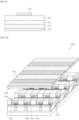
- FIG. 2 is a partial enlarged view of portion "A" in FIG. 1
- FIGS. 3A and 3B are cross-sectional views taken along lines B-B and C-C in FIG. 2
- FIG. 4 is a conceptual view illustrating a flip-chip type semiconductor light emitting device in FIG. 3A
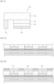
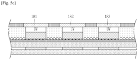
- FIGS. 5A through 5C are conceptual views illustrating various forms for implementing colors in connection with a flip-chip type semiconductor light emitting device.
- FIGS. 2 , 3A and 3B illustrate a display device 100 using a passive matrix (PM) type semiconductor light emitting device as a display device 100 using a semiconductor light emitting device.
- PM passive matrix
- AM active matrix
- the display device 100 includes a substrate 110, a first electrode 120, a conductive adhesive layer 130, a second electrode 140, and a plurality of semiconductor light emitting devices 150.
- the substrate 110 may be a flexible substrate.
- the substrate 110 may contain glass or polyimide (PI) to implement the flexible display device.
- PI polyimide
- any one such as polyethylene naphthalate (PEN), polyethylene terephthalate (PET) or the like may be used.
- the substrate 110 may be either one of transparent and non-transparent materials.
- the substrate 110 may be a wiring substrate disposed with the first electrode 120, and thus the first electrode 120 may be placed on the substrate 110.
- an insulating layer 160 is disposed on the substrate 110 placed with the first electrode 120, and an auxiliary electrode 170 is placed on the insulating layer 160.
- a configuration in which the insulating layer 160 is deposited on the substrate 110 may be single wiring substrate. More specifically, the insulating layer 160 may be incorporated into the substrate 110 with an insulating and flexible material such as polyimide (PI), PET, PEN or the like to form single wiring substrate.
- PI polyimide
- the auxiliary electrode 170 as an electrode for electrically connecting the first electrode 120 to the semiconductor light emitting device 150 is placed on the insulating layer 160, and disposed to correspond to the location of the first electrode 120.
- the auxiliary electrode 170 has a dot shape, and may be electrically connected to the first electrode 120 by an electrode hole 171 passing through the insulating layer 160.
- the electrode hole 171 can be formed by filling a conductive material in a via hole.
- the conductive adhesive layer 130 can be formed on one surface of the insulating layer 160, but the present disclosure is not limited to this.
- the conductive adhesive layer 130 may perform the role of an insulating layer in the structure in which the conductive adhesive layer 130 is disposed on the substrate 110.
- the conductive adhesive layer 130 may be a layer having adhesiveness and conductivity, and a conductive material and an adhesive material may be mixed on the conductive adhesive layer 130. Furthermore, the conductive adhesive layer 130 may have flexibility, thereby allowing a flexible function in the display device.
- the semiconductor light emitting devices may be connected in a flip chip form, and thus semiconductor light emitting devices grown on a transparent dielectric substrate. Furthermore, the semiconductor light emitting devices may be nitride semiconductor light emitting devices, for instance.
- the semiconductor light emitting device 150 has an excellent luminance characteristic, and thus it is possible to configure individual sub-pixels even with a small size thereof.
- the semiconductor light emitting device 150 is placed on the conductive adhesive layer 130 to configure a sub-pixel in the display device.
- the semiconductor light emitting device 150 may have excellent luminance characteristics, and thus it is possible to configure individual sub-pixels even with a small size thereof.
- the size of the individual semiconductor light emitting device 150 may be less than 80 ⁇ m in the length of one side thereof, and formed with a rectangular or square shaped element. In case of a rectangular shaped element, the size thereof may be less than 20 x 80 ⁇ m.
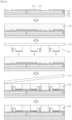
- FIG. 6 includes cross-sectional views illustrating a method of fabricating a display device using a semiconductor light emitting device.
- the conductive adhesive layer 130 is formed on the insulating layer 160 located with the auxiliary electrode 170 and second electrode 140.
- the insulating layer 160 is deposited on the first substrate 110 to form one substrate (or wiring substrate), and the first electrode 120, auxiliary electrode 170 and second electrode 140 are disposed at the wiring substrate.
- the first electrode 120 and second electrode 140 may be disposed in a perpendicular direction to each other.
- the first substrate 110 and insulating layer 160 may contain glass or polyimide (PI), respectively, to implement a flexible display device.
- the second substrate 112 is removed.
- the second substrate 112 may be removed using a laser lift-off (LLO) or chemical lift-off (CLO) method.
- LLO laser lift-off
- CLO chemical lift-off
- the second substrate 112 is removed to expose the semiconductor light emitting devices 150 to the outside.
- Silicon oxide (SiOx) or the like may be coated on the wiring substrate coupled to the semiconductor light emitting device 150 to form a transparent insulating layer.
- a phosphor layer can be formed on one surface of the semiconductor light emitting device 150.
- the semiconductor light emitting device 150 may be a blue semiconductor light emitting device for emitting blue (B) light, and red or green phosphor for converting the blue (B) light into the color of the sub-pixel may form a layer on one surface of the blue semiconductor light emitting device.
- the fabrication method or structure of a display device using the foregoing semiconductor light emitting device may be modified in various forms.
- the foregoing display device may be applicable to a vertical semiconductor light emitting device.
- the vertical structure will be described with reference to FIGS. 5 and 6 .
- the same or similar reference numerals are designated to the same or similar configurations to the foregoing example, and the description thereof will be substituted by the earlier description.
- the display device can use a passive matrix (PM) type of vertical semiconductor light emitting device.
- the display device includes a substrate 210, a first electrode 220, a conductive adhesive layer 230, a second electrode 240 and a plurality of semiconductor light emitting devices 250.
- the substrate 210 as a wiring substrate disposed with the first electrode 220 may include polyimide (PI) to implement a flexible display device. In addition, any one may be used if it is an insulating and flexible material.
- the first electrode 220 may be located on the substrate 210, and formed with a bar-shaped electrode elongated in one direction. The first electrode 220 can be formed to perform the role of a data electrode.
- the electrical connection is generated because an anisotropic conductive film partially has conductivity in the thickness direction when heat and pressure are applied as described above. Accordingly, the anisotropic conductive film is partitioned into a portion 231 having conductivity and a portion 232 having no conductivity in the thickness direction thereof.
- the semiconductor light emitting device 250 may have excellent luminance characteristics, and thus it is possible to configure individual sub-pixels even with a small size thereof.
- the size of the individual semiconductor light emitting device 250 may be less than 80 ⁇ m in the length of one side thereof, and formed with a rectangular or square shaped element. In case of a rectangular shaped element, the size thereof may be less than 20 ⁇ 80 ⁇ m.
- the semiconductor light emitting device 250 may be a vertical structure.
- a plurality of second electrodes 240 disposed in a direction of crossing the length direction of the first electrode 220, and electrically connected to the vertical semiconductor light emitting device 250 may be located between vertical semiconductor light emitting devices.
- a phosphor layer 280 can be formed on one surface of the semiconductor light emitting device 250.
- the semiconductor light emitting device 250 is a blue semiconductor light emitting device 251 that emits blue (B) light
- the phosphor layer 280 for converting the blue (B) light into the color of the sub-pixel may be provided thereon.
- the phosphor layer 280 may be a red phosphor 281 and a green phosphor 282 constituting individual pixels.
- a red phosphor 281 capable of converting blue light into red (R) light may be deposited on the blue semiconductor light emitting device 251 at a location implementing a red sub-pixel
- a green phosphor 282 capable of converting blue light into green (G) light may be deposited on the blue semiconductor light emitting device 251 at a location implementing a green sub-pixel.
- the blue semiconductor light emitting device 251 may be solely used at a location implementing a blue sub-pixel.
- the red (R), green (G) and blue (B) sub-pixels may implement one pixel.
- the present disclosure is not limited to this, and another structure for implementing blue, red and green may be also applicable thereto as described above in a display device to which a flip chip type light emitting device is applied.
- the second electrode 240 is located between the semiconductor light emitting devices 250, and electrically connected to the semiconductor light emitting devices 250.
- the semiconductor light emitting devices 250 may be disposed in a plurality of rows, and the second electrode 240 may be located between the rows of the semiconductor light emitting devices 250.
- the second electrode 240 may be located between the semiconductor light emitting devices 250.
- the second electrode 240 can be formed with a bar-shaped electrode elongated in one direction, and disposed in a perpendicular direction to the first electrode.
- the second electrode 240 may be electrically connected to the semiconductor light emitting device 250 by a connecting electrode protruded from the second electrode 240.
- the connecting electrode may be an n-type electrode of the semiconductor light emitting device 250.
- the n-type electrode is formed with an ohmic electrode for ohmic contact, and the second electrode covers at least part of the ohmic electrode by printing or deposition.
- the second electrode 240 may be electrically connected to the n-type electrode of the semiconductor light emitting device 250.
- the second electrode 240 may be located on the conductive adhesive layer 230.
- a transparent insulating layer containing silicon oxide (SiOx) can be formed on the substrate 210 formed with the semiconductor light emitting device 250.
- the transparent insulating layer is formed and then the second electrode 240 is placed thereon, the second electrode 240 may be located on the transparent insulating layer.
- the second electrode 240 can be formed to be separated from the conductive adhesive layer 230 or transparent insulating layer.
- a transparent electrode such as indium tin oxide (ITO) is used to locate the second electrode 240 on the semiconductor light emitting device 250
- the ITO material has a problem of bad adhesiveness with an n-type semiconductor. Accordingly, the second electrode 240 may be placed between the semiconductor light emitting devices 250, thereby obtaining an advantage in which the transparent electrode is not required. Accordingly, an n-type semiconductor layer and a conductive material having a good adhesiveness may be used as a horizontal electrode without being restricted by the selection of a transparent material, thereby enhancing the light extraction efficiency.
- a partition wall 290 can be formed between the semiconductor light emitting devices 250.
- the partition wall 290 may be disposed between the vertical semiconductor light emitting devices 250 to isolate the semiconductor light emitting device 250 constituting individual pixels.
- the partition wall 290 may perform the role of dividing individual sub-pixels from one another, and be formed as an integral body with the conductive adhesive layer 230.
- a base member of the anisotropic conductive film may form the partition wall when the semiconductor light emitting device 250 is inserted into the anisotropic conductive film.
- the partition wall 290 may have reflective characteristics while at the same time increasing contrast with no additional black insulator.
- a reflective partition wall may be separately provided with the partition wall 290.
- the partition wall 290 may include a black or white insulator according to the purpose of the display device.
- the partition wall 290 may be located between the semiconductor light emitting device 250 and second electrode 240. Accordingly, individual sub-pixels may be configured even with a small size using the semiconductor light emitting device 250, and a distance between the semiconductor light emitting devices 250 may be relatively sufficiently large to place the second electrode 240 between the semiconductor light emitting devices 250, thereby having the effect of implementing a flexible display device having a HD image quality.
- a black matrix 291 may be disposed between each phosphor layer to enhance contrast.
- the black matrix 191 can enhance the contrast of luminance.
- the semiconductor light emitting device 250 is located on the conductive adhesive layer 230, thereby constituting individual pixels on the display device.
- the semiconductor light emitting device 250 has excellent luminance characteristics, thereby configuring individual sub-pixels even with a small size thereof. As a result, it is possible to implement a full color display in which the sub-pixels of red (R), green (G) and blue (B) implement one pixel by the semiconductor light emitting device.
- the foregoing examples of the present disclosure have a passive matrix (PM) structure.
- the foregoing examples may be also applicable to an active matrix (AM) type semiconductor light emitting device, but in this instance, it may cause a problem in that a thin film transistor is damaged or destroyed during a bonding process of electrically connecting a wiring electrode to a semiconductor light emitting device.
- the present disclosure presents a mechanism capable of solving such a problem, and hereinafter, an embodiment of the present invention having the mechanism will be described.
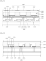
- FIG. 10 is an enlarged view illustrating portion "A" in FIG. 1 illustrating an embodiment of the present invention to which a novel type semiconductor light emitting device is applied
- FIGS. 11 and 12 are cross-sectional views of FIG. 10 .
- a display device 1000 using an active matrix type semiconductor light emitting device is illustrated as a display device 1000 using a semiconductor light emitting device.
- the display device 1000 forms a structure in which a plurality of semiconductor light emitting devices 1050 are electrically connected to a first electrode 1020 and a second electrode 1040 formed on a substrate 1010.
- the substrate 1010 as a wiring substrate on which the first electrode 1020 is disposed may include polyimide (PI) to implement a flexibly display device.
- PI polyimide
- any material may be used for the substrate 1010 if it is an insulating and flexible material.
- the semiconductor light emitting device 1050 may be a flip chip type light emitting device. However, the present disclosure is not limited to this, and a semiconductor light emitting device with a vertical type structure may be used.
- the semiconductor light emitting device 1050 includes a first conductive electrode 1156, a first conductive semiconductor layer 1155 formed with the first conductive electrode 1156, an active layer 1154 formed on the first conductive semiconductor layer 1155, and a second conductive semiconductor layer 1153 formed on the active layer 1154 and a second conductive electrode 1152 formed on the second conductive semiconductor layer 1153.
- first conductive electrode 1156 and first conductive semiconductor layer 1155 may be a p-type electrode and a p-type semiconductor layer, respectively
- second conductive electrode 1152 and second conductive semiconductor layer 1153 may be an n-type electrode and an n-type semiconductor layer, respectively.
- present disclosure is not limited to this, and may also have an illustration in which the first conductive type is an n-type and the second conductive type is a p-type.
- the first electrode 1020 as a pixel electrode provided for each pixel is electrically connected to the first conductive electrode 1156.
- the second electrode 1040 may be a common electrode electrically connected to the second conductive electrode 1152.
- the second electrode 1040 may include a plurality of electrode lines.
- the semiconductor light emitting device 1050 is electrically connected to a common electrode and a pixel electrode portion provided for each pixel to form an individual pixel.
- a blue light emitting diode for emitting blue light may be used for the semiconductor light emitting device 1050, and a phosphor layer 1080 capable of converting a wavelength of light emitted from the light emitting device 1050 may be located on the semiconductor light emitting device 1050.
- the phosphor layer 1080 may be a yellow phosphor layer capable of converting blue light into white light when mixed with the blue light.
- a color filter portion 1090 may be disposed to cover the semiconductor light emitting device to implement three primary colors such as red (R), green (G) and blue (B) using white light converted by the phosphor layer 1080.
- a red (R) filter 1091, a green (G) filter 1092, and a blue (B) filter 1093 may be provided thereon, and a pixel formed by each light emitting device may form a sub-pixel, and such three sub-pixels may form a pixel.
- the display device may further include a black matrix 1094 disposed between each filter to enhance the contrast of the color filter portion 1090.
- the black matrix 1094 can be formed so a gap is made between filters, and a black material fills into the gap. Through this, the black matrix 1094 may enhance the contrast between light and shade while at the same time absorbing external light reflection.
- the pixel electrode portion is connected to a thin film transistor (TFT) 1100 to implement an active matrix type display.
- TFT thin film transistor
- the thin film transistor 1100 has a source region 1101, a drain region 1103 and a channel region 1104, and a gate electrode 1102 is located in the channel region 1104.
- the source region 1101 is electrically connected to the pixel electrode portion to actively control a pixel to be emitted by the driving of the thin film transistor 1100.
- the thin film transistor 1100 is coated by an interlayer insulating layer 1120.
- a gap between individual thin film transistors 1100 may be large, and the interlayer insulating layer 1120 is disposed between the gap.
- a sub-pixel having a sufficient brightness may be implemented using a semiconductor light emitting device in a small size to increase a distance between individual pixels, thereby implementing a flexible display device due to the increased distance.
- an electrical connection between the semiconductor light emitting device 1050 and the pixel electrode portion and common electrode may be performed by the conductive adhesive layer 1030.
- the conductive adhesive layer 1030 may be an anisotropy conductive film (ACF), an anisotropy conductive paste, a solution containing conductive particles, or the like.
- the conductive adhesive layer 1030 can be formed of a non-transparent material to prevent the semiconductor light emitting devices from causing interference of mixed colors therebetween.
- the process of placing an anisotropy conductive film or the like onto the pixel electrode portion and common electrode, and then applying heat or pressure to the semiconductor light emitting device 1050 to bond them to each other may be performed.
- an anisotropy conductive film is placed between the interlayer insulating layer 1120 and the semiconductor light emitting device 1050, it may cause a problem in that the thin film transistor or semiconductor light emitting device is destroyed due to adhesion between ceramic thin films.
- a buffer layer 1200 is disposed between the thin film transistor 1100 and the conductive adhesive layer 1030.
- the buffer layer 1200 is formed of an elastic material to protect the thin film transistor (or semiconductor light emitting device).
- the buffer layer 1200 is disposed on the interlayer insulating layer of the thin film transistor, and may be formed of a polymer based or epoxy based material having an elasticity.
- the buffer layer 1200 can be formed of a material with a higher elasticity than that of the interlayer insulating layer of the thin film transistor.
- the buffer layer 1200 can be formed of a material with a low strength than that of the interlayer insulating layer.
- the buffer layer 1200 may include a polymer based material having an adhesiveness along with an elasticity.
- the buffer layer 1200 may be disposed at an opposite side to the color filter portion 1090 based on the semiconductor light emitting device 1050, and have a non-transparent property.
- the buffer layer may include a white colored material to reflect light emitted from the semiconductor light emitting device or include a black colored material to absorb the light so as to increase contrast ratio.
- the pixel electrode portion is disposed on the buffer layer 1200, and electrically connected to the semiconductor light emitting device through the conductive adhesive layer 1030. More specifically, the pixel electrode portion includes a first pixel electrode 1021 and a second pixel electrode 1022.
- the first pixel electrode 1021 is an electrode disposed on the interlayer insulating layer 1120 of the thin film transistor 1100.
- a source region 1101 of the thin film transistor 1100 is electrically connected to the first pixel electrode 1021.
- the source region 1101 and first pixel electrode 1021 may be electrically connected to each other by a through electrode 1131 passing through the interlayer insulating layer 1120.
- the second pixel electrode 1022 is extended to one surface of the buffer layer 1200 through the buffer layer 1200 from the first pixel electrode 1021.
- One surface of the buffer layer 1200 is a surface covered by the conductive adhesive layer 1030, and the other surface that is an opposite surface to the one surface of the buffer layer 1200 is a portion for covering the interlayer insulating layer 1120.
- the first pixel electrode 1021 is disposed at a side of the other surface of the buffer layer 1200, and the second pixel electrode 1022 is extended from the other surface of the buffer layer 1200 to one surface thereof, and at least part thereof is inserted into the conductive adhesive layer 1030.
- the second pixel electrode 1022 can be electrically connected to the first conductive electrode 1156 of the semiconductor light emitting device 1050.
- At least one common electrode can be formed on one surface of the buffer layer 1200.
- a plurality of electrode lines of the second electrode 1040 formed as the common electrode are disposed on one surface of the buffer layer 1200, and electrically connected to the second conductive electrode 1152 of the semiconductor light emitting device through the conductive adhesive layer 1030.
- defects due to a crack can be reduced by the buffering of the buffer layer, thereby enhancing a yield during a wiring process of the display device, and implementing an electrical connection path with higher reliability.
- the buffer layer described in the present example may be applicable to various types of display devices.
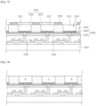
- FIGS. 13 and 14 are cross-sectional views illustrating another embodiment of the present invention.
- a structure in which a phosphor layer implements three primary colors such as red (R), green (G) and blue (B) instead of a color filter portion in the foregoing example with reference to FIGS. 10 , 11 and 12 is allowed.
- the foregoing structure described above with reference to FIGS. 10 , 11 and 12 may be applicable to a structure including a first electrode 2020, a second electrode, a light emitting device 2050, a conductive adhesive layer 2030, a thin film transistor passive safely system 2100, a buffer layer 2200, and the like, and the description thereof will be substituted by the earlier description.
- a phosphor layer 2080 may be located on an outer surface of the semiconductor light emitting device 2050.
- the semiconductor light emitting device 2050 is a blue semiconductor light emitting device for emitting blue (B) light
- the phosphor layer 2080 performs a function of converting the blue (B) light into the color of a sub-pixel.
- the phosphor layer 2080 may be a red phosphor 2081 or green phosphor 2082 constituting an individual pixel.
- a blue semiconductor light emitting device may be disposed below the red phosphor 2081 or green phosphor 2082, and the conductive adhesive layer 2030, buffer layer 2200 and thin film transistor 2100 may be sequentially disposed below the blue semiconductor light emitting device.
- the red phosphor 2081 capable of converting blue light to red (R) light may be deposited on a blue semiconductor light emitting device 2051 at a position for implementing a red sub-pixel
- the green phosphor 2082 capable of converting blue light to green (G) light may be deposited on a blue semiconductor light emitting device 2051 at a position for implementing a green sub-pixel.
- only the blue semiconductor light emitting device 2051 may be exclusively used at a portion for implementing a blue sub-pixel.
- sub-pixels such as red (R), green (G) and blue (B) may implement one pixel.
- a black matrix 2094 may be disposed between each phosphor layer to enhance contrast.
- the black matrix 2094 may enhance the contrast of brightness. Referring to FIG. 14 , a structure in which each semiconductor light emitting device 3050 implements three primary colors such as red (R), green (G) and blue (B) without a color filter portion in the foregoing example with reference to FIGS. 10 , 11 and 12 is allowed.
- each semiconductor light emitting device 2050 indium (In) and/or aluminum (Al) are added together to a base material of gallium nitride (GaN) to implement a high-power light emitting device for emitting various lights including blue.
- the semiconductor light emitting device 2050 may be a red, a green or a blue semiconductor light emitting device to implement each sub-pixel.
- the red, green and blue semiconductor light emitting devices (R, G, B) are alternately disposed, and red, green and blue sub-pixels constitute one pixel by the red, green and blue semiconductor light emitting devices, thereby implementing a full color display.
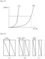
- FIG. 15 is a graph illustrating a margin of gradation expression
- FIG. 16 is a conceptual view illustrating a control method associated with the present disclosure
- FIG. 17 is a circuit diagram illustrating implementing a control method of FIG. 16 .
- a small-sized light emitting diode (ultra light emitting diode, ULED) is very narrow compared to an organic electro-luminescence device (OLED).
- ULED ultra light emitting diode
- OLED organic electro-luminescence device
- a margin to the operating voltage thereof is small in case of the ultra light emitting diode since it reaches a target current value even at a small operating voltage. Accordingly, another method is required due to a small operation voltage margin to express gradation using the ultra light emitting diode.
- the ultra light emitting diode can be controlled such that an operating frequency thereof varies according to a level of gradation.
- gradation expression is divided by frequencies.
- the level of gradation is partitioned into a first level with a high gradation ( FIG. 16A ), a second level with a middle gradation, and a third level with a low gradation ( FIG. 16B ), and the operating frequency of the first level is lower than that of the third level ( FIG. 16C ), and an operating frequency of the first level is lower than that of the third level.
- the first level corresponds to a high gradation, and operates at a frequency of 120 Hz.
- the second level is a middle gradation, and operates at frequencies of 120 to 240 Hz
- the third level is a low gradation, and operates at a frequency of 240 Hz.
- the second level or third level may have an idle time during an operating period of the semiconductor light emitting device.
- a frequency modulator may be provided in an AM equivalent circuit in the present example as illustrated in FIG. 17 .
- gradation may be partitioned into any levels, and a higher frequency, for example, above 120 Hz, may be used and an idle time may be applied to a low gradation, thereby maximizing gradation expression power.
- an impact applied to the display device can be decentralized during a bonding process of wiring electrodes and semiconductor light emitting devices by a buffer layer.
- a buffer layer can alleviate or prevent a thin film transistor from being damaged or destroyed during the bonding process.
- defects due to a crack can be reduced by the buffering of a buffer layer, thereby enhancing a yield during a wiring process of the display device, and implementing an electrical connection path with higher reliability.
- An operating frequency of the semiconductor light emitting device may vary, thereby solving a problem of causing restriction in gradation expression power.
Landscapes
- Engineering & Computer Science (AREA)
- Microelectronics & Electronic Packaging (AREA)
- Physics & Mathematics (AREA)
- Computer Hardware Design (AREA)
- General Physics & Mathematics (AREA)
- Theoretical Computer Science (AREA)
- Electroluminescent Light Sources (AREA)
- Devices For Indicating Variable Information By Combining Individual Elements (AREA)
- Manufacturing & Machinery (AREA)
Claims (13)
- Anzeigevorrichtung, umfassend:einen Pixelelektrodenabschnitt, der elektrisch mit einem Dünnschichttransistor (1100, 2100) mit einer Gate-Elektrode (1102) verbunden ist;eine lichtemittierende Halbleitervorrichtung (1050, 2050), die dazu eingerichtet ist, Licht zu emittieren, um ein einzelnes Pixel zu bilden, und die eine leitende Elektrode (1152, 1156) enthält;eine leitende Klebeschicht (1030, 2030), die an der lichtemittierenden Halbleitervorrichtung (1050, 2050) haftet und dazu eingerichtet ist, den Pixelelektrodenabschnitt mit der leitenden Elektrode elektrisch zu verbinden;eine isolierende Zwischenschicht (1120) auf dem Dünnschichttransistor (1100, 2100); undeine Pufferschicht (1200, 2200), die ein elastisches Material enthält und zwischen der isolierenden Zwischenschicht (1120) und der leitenden Klebeschicht (1030, 2030) angeordnet ist, wobei eine Oberfläche der Pufferschicht eine Oberfläche ist, die von der leitenden Klebeschicht bedeckt ist, und eine andere Oberfläche der Pufferschicht, die eine der einen Oberfläche gegenüberliegende Oberfläche ist, ein Abschnitt zum Bedecken der isolierenden Zwischenschicht ist, wobei der Pixelelektrodenabschnitt eine erste Pixelelektrode (1021), die auf der isolierenden Zwischenschicht (1120) des Dünnfilmtransistors (1100, 2100) angeordnet ist, und eine zweite Pixelelektrode (1022) umfasst, die sich von der ersten Pixelelektrode durch die Pufferschicht zu einer Oberfläche der Pufferschicht (1200) erstreckt.
- Anzeigevorrichtung nach Anspruch 1, wobei das elastische Material ein Material auf Polymer- oder Epoxidbasis enthält,
wobei das Material auf Polymerbasis ein Klebevermögen aufweist. - Anzeigevorrichtung nach Anspruch 1, wobei das elastische Material eine höhere Elastizität als die isolierende Zwischenschicht (1120) aufweist.
- Anzeigevorrichtung nach Anspruch 1, ferner umfassend:
einen Farbfilterabschnitt (1090), der die lichtemittierende Halbleitervorrichtung abdeckt, um Rot (R), Grün (G) und Blau (B) zu realisieren. - Anzeigevorrichtung nach Anspruch 4, wobei die Pufferschicht (1200) auf einer dem Farbfilterabschnitt (1090) gegenüberliegenden Seite auf der Basis der lichtemittierenden Halbleitervorrichtung (1050) angeordnet ist und eine nichttransparente Eigenschaft aufweist.
- Anzeigevorrichtung nach Anspruch 1, wobei die Pufferschicht (1200) dazu eingerichtet ist, von der lichtemittierenden Halbleitervorrichtung (1050) emittiertes Licht zu reflektieren.
- Anzeigevorrichtung nach Anspruch 6, wobei die Pufferschicht (1200) ein weißes Material enthält.
- Anzeigevorrichtung nach Anspruch 1, ferner umfassend:eine Durchgangselektrode (1131), die in der isolierenden Zwischenschicht (1120) angeordnet ist, um einen Source-Bereich (1101) des Dünnfilmtransistors und die erste Pixelelektrode (1021) elektrisch zu verbinden, undwobei sich die Pufferschicht nicht vertikal mit der Durchgangselektrode überlappt.
- Anzeigevorrichtung nach Anspruch 1, ferner umfassend:
mindestens eine gemeinsame Elektrode (1040) auf einer Oberfläche der Pufferschicht. - Anzeigevorrichtung nach Anspruch 9, wobei die zweite Pixelelektrode (1022) elektrisch mit einer ersten leitenden Elektrode (1156) der lichtemittierenden Halbleitervorrichtung (1050) verbunden ist, und
wobei die gemeinsame Elektrode (1040) elektrisch mit einer zweiten leitenden Elektrode (1152) der lichtemittierenden Halbleitervorrichtung (1050) verbunden ist. - Anzeigevorrichtung nach Anspruch 1, wobei zumindest ein Teil der zweiten Pixelelektrode (1022) in die leitende Klebeschicht (1030) eingesetzt ist.
- Verfahren zur Herstellung einer Anzeigevorrichtung, wobei das Verfahren umfasst:Ausbilden einer Mehrzahl von Dünnschichttransistoren (1100) mit einer Gate-Elektrode (1102) auf einem Substrat (1010);Ausbilden einer isolierenden Zwischenschicht (1120) auf der Mehrzahl von Dünnschichttransistoren (1100);Ausbilden einer Pufferschicht (1200) auf der isolierenden Zwischenschicht (1120);Ausbilden einer Mehrzahl von Pixelelektrodenabschnitten, die elektrisch mit entsprechenden Dünnfilmtransistoren (1100) verbunden sind, wobei jeder Pixelelektrodenabschnitt eine erste Pixelelektrode (1021), die auf der isolierenden Zwischenschicht (1120) angeordnet ist, und eine zweite Pixelelektrode (1022) enthält, die sich von der ersten Pixelelektrode (1021) durch die Pufferschicht (1200) hindurch zu einer Oberfläche der Pufferschicht (1200) erstreckt; undAusbilden einer Mehrzahl von lichtemittierenden Halbleitervorrichtungen (1050), die dazu eingerichtet sind, Licht zu emittieren, mit einer leitenden Klebeschicht (1030), die an entsprechenden lichtemittierenden Halbleitervorrichtungen haftet, um entsprechende Pixelelektrodenabschnitte mit entsprechenden leitenden Elektroden der Mehrzahl von lichtemittierenden Halbleitervorrichtungen elektrisch zu verbinden,wobei die Pufferschicht (1200) ein elastisches Material enthält und zwischen der isolierenden Zwischenschicht (1120) und der leitenden Klebeschicht (1030) angeordnet ist, wobei eine Oberfläche der Pufferschicht eine Oberfläche ist, die von der leitenden Klebeschicht bedeckt ist, und eine andere Oberfläche der Pufferschicht, die eine der einen Oberfläche gegenüberliegende Oberfläche ist, ein Abschnitt zum Bedecken der isolierenden Zwischenschicht ist.
- Verfahren nach Anspruch 12, wobei das elastische Material ein Material auf Polymerbasis oder Epoxidbasis enthält und das Material auf Polymerbasis eine Klebefähigkeit aufweist.
Applications Claiming Priority (2)
| Application Number | Priority Date | Filing Date | Title |
|---|---|---|---|
| KR1020160006120A KR102591388B1 (ko) | 2016-01-18 | 2016-01-18 | 반도체 발광 소자를 이용한 디스플레이 장치 |
| PCT/KR2016/009607 WO2017126762A1 (en) | 2016-01-18 | 2016-08-29 | Display device using semiconductor light emitting device |
Publications (3)
| Publication Number | Publication Date |
|---|---|
| EP3406110A1 EP3406110A1 (de) | 2018-11-28 |
| EP3406110A4 EP3406110A4 (de) | 2019-10-02 |
| EP3406110B1 true EP3406110B1 (de) | 2024-08-21 |
Family
ID=59313940
Family Applications (1)
| Application Number | Title | Priority Date | Filing Date |
|---|---|---|---|
| EP16886605.1A Active EP3406110B1 (de) | 2016-01-18 | 2016-08-29 | Anzeigevorrichtung mit lichtemittierendem halbleiterbauelement |
Country Status (4)
| Country | Link |
|---|---|
| US (1) | US9825067B2 (de) |
| EP (1) | EP3406110B1 (de) |
| KR (1) | KR102591388B1 (de) |
| WO (1) | WO2017126762A1 (de) |
Families Citing this family (43)
| Publication number | Priority date | Publication date | Assignee | Title |
|---|---|---|---|---|
| US10332949B2 (en) | 2016-07-06 | 2019-06-25 | Seoul Semiconductor Co., Ltd. | Display apparatus |
| US10593657B2 (en) * | 2016-11-01 | 2020-03-17 | Innolux Corporation | Display devices and methods for forming the same |
| KR102650341B1 (ko) * | 2016-11-25 | 2024-03-22 | 엘지전자 주식회사 | 반도체 발광 소자를 이용한 디스플레이 장치 및 이의 제조방법 |
| KR102555383B1 (ko) * | 2016-12-07 | 2023-07-12 | 엘지디스플레이 주식회사 | 유기발광소자를 이용한 조명장치 및 그 제조방법 |
| KR102732021B1 (ko) * | 2016-12-26 | 2024-11-21 | 삼성디스플레이 주식회사 | 표시 장치 |
| CN111048656B (zh) * | 2017-09-04 | 2024-06-14 | 首尔半导体株式会社 | 显示装置及该显示装置的制造方法 |
| KR102476136B1 (ko) * | 2017-09-05 | 2022-12-09 | 삼성전자주식회사 | Led를 이용한 디스플레이 장치 |
| KR102650950B1 (ko) | 2017-09-29 | 2024-03-26 | 서울반도체 주식회사 | 발광 소자 및 그것을 갖는 표시 장치 |
| KR102515399B1 (ko) * | 2017-12-12 | 2023-03-28 | 엘지디스플레이 주식회사 | 배선 필름 및 그를 포함한 표시 장치 |
| US11335835B2 (en) | 2017-12-20 | 2022-05-17 | Lumileds Llc | Converter fill for LED array |
| US11355549B2 (en) * | 2017-12-29 | 2022-06-07 | Lumileds Llc | High density interconnect for segmented LEDs |
| CN110112123A (zh) * | 2018-02-01 | 2019-08-09 | 晶元光电股份有限公司 | 发光装置及其制造方法 |
| KR102551354B1 (ko) * | 2018-04-20 | 2023-07-04 | 삼성전자 주식회사 | 반도체 발광 소자 및 그 제조 방법 |
| JP7267683B2 (ja) * | 2018-04-25 | 2023-05-02 | シャープ株式会社 | 発光素子モジュール |
| WO2019220246A1 (ja) * | 2018-05-18 | 2019-11-21 | 株式会社半導体エネルギー研究所 | 表示装置、表示モジュール、電子機器、及び、表示装置の作製方法 |
| KR20190137458A (ko) | 2018-06-01 | 2019-12-11 | 삼성전자주식회사 | Led를 이용한 디스플레이 모듈 제조방법 |
| US10886447B2 (en) * | 2018-09-14 | 2021-01-05 | Seoul Viosys Co., Ltd. | Light emitting device |
| CN109300931B (zh) * | 2018-09-30 | 2021-02-26 | 上海天马微电子有限公司 | 一种Micro LED显示面板及制作方法、显示装置 |
| KR102658265B1 (ko) * | 2018-11-15 | 2024-04-18 | 삼성전자주식회사 | 접합 부재 상에 무기 발광 소자 및 차광 부재를 포함하는 디스플레이 모듈 및 디스플레이 장치 |
| KR102555828B1 (ko) * | 2018-12-17 | 2023-07-13 | 엘지디스플레이 주식회사 | 고 해상도 마이크로 led 표시 장치 및 그 제조 방법 |
| US10910433B2 (en) * | 2018-12-31 | 2021-02-02 | Lumileds Llc | Pixelated LED array with optical elements |
| TWI705579B (zh) * | 2019-07-19 | 2020-09-21 | 李蕙如 | 主動式rgb發光二極體顯示器載板 |
| CN112289819A (zh) * | 2019-07-25 | 2021-01-29 | 李蕙如 | 主动式rgb发光二极管显示器载板 |
| WO2021020393A1 (ja) * | 2019-07-30 | 2021-02-04 | 日亜化学工業株式会社 | 画像表示装置の製造方法および画像表示装置 |
| KR102905065B1 (ko) * | 2019-08-06 | 2025-12-29 | 엘지전자 주식회사 | 반도체 발광 소자를 이용한 디스플레이 장치 |
| US11201200B2 (en) * | 2019-08-23 | 2021-12-14 | Advanced Semiconductor Engineering, Inc. | Semiconductor device package and method of manufacturing the same |
| TWI736982B (zh) * | 2019-09-17 | 2021-08-21 | 李蕙如 | 主動式rgb發光二極體像素元件 |
| CN112542478A (zh) * | 2019-09-23 | 2021-03-23 | 李蕙如 | 主动式rgb发光二极管像素组件 |
| KR102737511B1 (ko) * | 2019-10-29 | 2024-12-05 | 삼성전자주식회사 | Led 모듈 및 제조방법 |
| CN111261658B (zh) * | 2020-02-10 | 2023-02-28 | Tcl华星光电技术有限公司 | 微型发光二极管显示面板及微型发光二极管的转印方法 |
| US11817535B2 (en) * | 2020-04-21 | 2023-11-14 | Raysolve Optoelectronics (Suzhou) Company Limited | Light emitting diode structure and method for manufacturing the same |
| US12527137B2 (en) * | 2020-04-21 | 2026-01-13 | Raysolve Optoelectronics (Suzhou) Company Limited | Light emitting diode structure and method for manufacturing the same |
| US11980046B2 (en) | 2020-05-27 | 2024-05-07 | Taiwan Semiconductor Manufacturing Company, Ltd. | Method for forming an isolation structure having multiple thicknesses to mitigate damage to a display device |
| CN112259692A (zh) * | 2020-10-13 | 2021-01-22 | 武汉华星光电半导体显示技术有限公司 | 柔性显示面板及显示装置 |
| KR102944421B1 (ko) * | 2020-10-22 | 2026-03-27 | 삼성디스플레이 주식회사 | 표시 장치 |
| KR102868772B1 (ko) * | 2020-10-27 | 2025-10-13 | 삼성전자주식회사 | 디스플레이 모듈 및 그 제조 방법 |
| TWI755946B (zh) | 2020-11-24 | 2022-02-21 | 財團法人工業技術研究院 | 電子裝置及具有其之透明顯示器 |
| FR3119709B1 (fr) * | 2021-02-09 | 2023-10-20 | Commissariat Energie Atomique | Diode electroluminescente comprenant des regions emissives incluant des ions de terres rares |
| US12193180B2 (en) * | 2021-06-15 | 2025-01-07 | Innolux Corporation | Electronic device |
| TWI792460B (zh) * | 2021-07-28 | 2023-02-11 | 友達光電股份有限公司 | 顯示面板及其製造方法 |
| KR102887715B1 (ko) * | 2021-08-10 | 2025-11-18 | 삼성디스플레이 주식회사 | 표시 장치 |
| CN117080346A (zh) * | 2022-12-30 | 2023-11-17 | 天马新型显示技术研究院(厦门)有限公司 | 发光元件封装结构、显示面板、显示装置以及制备方法 |
| CN116053387A (zh) * | 2023-03-07 | 2023-05-02 | 惠科股份有限公司 | 显示面板制作方法与显示面板 |
Citations (1)
| Publication number | Priority date | Publication date | Assignee | Title |
|---|---|---|---|---|
| KR20130137985A (ko) * | 2012-06-08 | 2013-12-18 | 엘지전자 주식회사 | 반도체 발광 소자를 이용한 디스플레이 장치 |
Family Cites Families (9)
| Publication number | Priority date | Publication date | Assignee | Title |
|---|---|---|---|---|
| JP3808060B2 (ja) * | 2003-06-23 | 2006-08-09 | ローム株式会社 | 半導体集積回路装置 |
| US8149346B2 (en) * | 2005-10-14 | 2012-04-03 | Semiconductor Energy Laboratory Co., Ltd. | Display device and manufacturing method thereof |
| KR20080002338A (ko) | 2006-06-30 | 2008-01-04 | 엘지.필립스 엘시디 주식회사 | 유기 전계발광 표시장치와 그의 제조 방법 |
| US20130308076A1 (en) | 2010-10-01 | 2013-11-21 | Sharp Kabushiki Kaisha | Flexible display and method for manufacturing the same |
| KR101452768B1 (ko) | 2012-08-21 | 2014-10-21 | 엘지전자 주식회사 | 반도체 발광 소자를 이용한 디스플레이 장치 및 이의 제조방법 |
| KR101476686B1 (ko) * | 2013-04-01 | 2014-12-26 | 엘지전자 주식회사 | 반도체 발광 소자를 이용한 디스플레이 장치 |
| KR102135352B1 (ko) * | 2013-08-20 | 2020-07-17 | 엘지전자 주식회사 | 표시장치 |
| GB2525605B (en) | 2014-04-28 | 2018-10-24 | Flexenable Ltd | Method of bonding flexible printed circuits |
| KR102014258B1 (ko) * | 2014-11-21 | 2019-08-26 | 엘지전자 주식회사 | 반도체 발광 소자를 이용한 디스플레이 장치 및 이의 제조방법 |
-
2016
- 2016-01-18 KR KR1020160006120A patent/KR102591388B1/ko active Active
- 2016-07-08 US US15/205,729 patent/US9825067B2/en active Active
- 2016-08-29 EP EP16886605.1A patent/EP3406110B1/de active Active
- 2016-08-29 WO PCT/KR2016/009607 patent/WO2017126762A1/en not_active Ceased
Patent Citations (1)
| Publication number | Priority date | Publication date | Assignee | Title |
|---|---|---|---|---|
| KR20130137985A (ko) * | 2012-06-08 | 2013-12-18 | 엘지전자 주식회사 | 반도체 발광 소자를 이용한 디스플레이 장치 |
Also Published As
| Publication number | Publication date |
|---|---|
| EP3406110A4 (de) | 2019-10-02 |
| KR20170086366A (ko) | 2017-07-26 |
| WO2017126762A1 (en) | 2017-07-27 |
| KR102591388B1 (ko) | 2023-10-19 |
| US9825067B2 (en) | 2017-11-21 |
| EP3406110A1 (de) | 2018-11-28 |
| US20170207249A1 (en) | 2017-07-20 |
Similar Documents
| Publication | Publication Date | Title |
|---|---|---|
| EP3406110B1 (de) | Anzeigevorrichtung mit lichtemittierendem halbleiterbauelement | |
| US12074147B2 (en) | Display device using semiconductor light-emitting element and manufacturing method therefor | |
| EP2981952B1 (de) | Anzeigevorrichtung mit lichtemittierendem halbleiterbauelement | |
| EP3573431B1 (de) | Anzeigevorrichtung mit verwendung von lichtemittierendem halbleiterelement | |
| US9082947B2 (en) | Display device using semiconductor light emitting device | |
| US10770631B2 (en) | Display apparatus using semi-conductor light-emitting device | |
| US9257482B2 (en) | Display device using semiconductor light emitting device | |
| US9865572B2 (en) | Display device using semiconductor light emitting device and method for manufacturing | |
| US9206967B2 (en) | Display device using semiconductor light emitting device | |
| US9502389B2 (en) | Display device using semiconductor light emitting device | |
| US9406656B2 (en) | Display device using semiconductor light emitting device and method of fabricating the same | |
| US9093629B2 (en) | Display device using semiconductor light emitting device and method of fabricating the same | |
| US9842764B2 (en) | Display device using semiconductor light emitting devices and method for manufacturing the same | |
| EP3602630B1 (de) | Anzeigevorrichtung mit lichtemittierendem halbleiterbauelement | |
| CN112567522A (zh) | 使用半导体发光二极管的显示装置及其制造方法 | |
| US10276632B2 (en) | Display device using semiconductor light-emitting diodes, and manufacturing method therefor | |
| US20220123175A1 (en) | Display device employing semiconductor light-emitting element and manufacturing method therefor | |
| US12593727B2 (en) | Display device using semiconductor light-emitting diodes, and method for manufacturing same |
Legal Events
| Date | Code | Title | Description |
|---|---|---|---|
| STAA | Information on the status of an ep patent application or granted ep patent |
Free format text: STATUS: THE INTERNATIONAL PUBLICATION HAS BEEN MADE |
|
| PUAI | Public reference made under article 153(3) epc to a published international application that has entered the european phase |
Free format text: ORIGINAL CODE: 0009012 |
|
| STAA | Information on the status of an ep patent application or granted ep patent |
Free format text: STATUS: REQUEST FOR EXAMINATION WAS MADE |
|
| 17P | Request for examination filed |
Effective date: 20180807 |
|
| AK | Designated contracting states |
Kind code of ref document: A1 Designated state(s): AL AT BE BG CH CY CZ DE DK EE ES FI FR GB GR HR HU IE IS IT LI LT LU LV MC MK MT NL NO PL PT RO RS SE SI SK SM TR |
|
| AX | Request for extension of the european patent |
Extension state: BA ME |
|
| DAV | Request for validation of the european patent (deleted) | ||
| DAX | Request for extension of the european patent (deleted) | ||
| A4 | Supplementary search report drawn up and despatched |
Effective date: 20190903 |
|
| RIC1 | Information provided on ipc code assigned before grant |
Ipc: H01L 33/12 20100101ALI20190828BHEP Ipc: H05B 33/14 20060101AFI20190828BHEP Ipc: H01L 33/00 20100101ALI20190828BHEP Ipc: H01L 33/58 20100101ALI20190828BHEP Ipc: H05B 37/00 20060101ALI20190828BHEP |
|
| STAA | Information on the status of an ep patent application or granted ep patent |
Free format text: STATUS: EXAMINATION IS IN PROGRESS |
|
| 17Q | First examination report despatched |
Effective date: 20211206 |
|
| REG | Reference to a national code |
Ref country code: DE Free format text: PREVIOUS MAIN CLASS: H05B0033140000 Ipc: H10K0059123000 Ref legal event code: R079 Ref document number: 602016089051 Country of ref document: DE |
|
| GRAP | Despatch of communication of intention to grant a patent |
Free format text: ORIGINAL CODE: EPIDOSNIGR1 |
|
| STAA | Information on the status of an ep patent application or granted ep patent |
Free format text: STATUS: GRANT OF PATENT IS INTENDED |
|
| RIC1 | Information provided on ipc code assigned before grant |
Ipc: H05K 3/32 20060101ALN20240226BHEP Ipc: H01L 33/62 20100101ALN20240226BHEP Ipc: H01L 33/44 20100101ALN20240226BHEP Ipc: H01L 25/16 20060101ALI20240226BHEP Ipc: H01L 25/075 20060101ALI20240226BHEP Ipc: H01L 27/12 20060101ALI20240226BHEP Ipc: G09G 3/3233 20160101ALI20240226BHEP Ipc: H10K 59/129 20230101ALI20240226BHEP Ipc: H10K 59/124 20230101ALI20240226BHEP Ipc: H10K 59/123 20230101AFI20240226BHEP |
|
| INTG | Intention to grant announced |
Effective date: 20240320 |
|
| RIC1 | Information provided on ipc code assigned before grant |
Ipc: H10K 59/179 20230101ALN20240308BHEP Ipc: H10K 59/131 20230101ALN20240308BHEP Ipc: H05K 3/32 20060101ALN20240308BHEP Ipc: H01L 33/62 20100101ALN20240308BHEP Ipc: H01L 33/44 20100101ALN20240308BHEP Ipc: H01L 25/16 20060101ALI20240308BHEP Ipc: H01L 25/075 20060101ALI20240308BHEP Ipc: H01L 27/12 20060101ALI20240308BHEP Ipc: G09G 3/3233 20160101ALI20240308BHEP Ipc: H10K 59/129 20230101ALI20240308BHEP Ipc: H10K 59/124 20230101ALI20240308BHEP Ipc: H10K 59/123 20230101AFI20240308BHEP |
|
| GRAS | Grant fee paid |
Free format text: ORIGINAL CODE: EPIDOSNIGR3 |
|
| GRAA | (expected) grant |
Free format text: ORIGINAL CODE: 0009210 |
|
| STAA | Information on the status of an ep patent application or granted ep patent |
Free format text: STATUS: THE PATENT HAS BEEN GRANTED |
|
| AK | Designated contracting states |
Kind code of ref document: B1 Designated state(s): AL AT BE BG CH CY CZ DE DK EE ES FI FR GB GR HR HU IE IS IT LI LT LU LV MC MK MT NL NO PL PT RO RS SE SI SK SM TR |
|
| REG | Reference to a national code |
Ref country code: GB Ref legal event code: FG4D |
|
| REG | Reference to a national code |
Ref country code: CH Ref legal event code: EP |
|
| REG | Reference to a national code |
Ref country code: IE Ref legal event code: FG4D |
|
| REG | Reference to a national code |
Ref country code: DE Ref legal event code: R096 Ref document number: 602016089051 Country of ref document: DE |
|
| REG | Reference to a national code |
Ref country code: LT Ref legal event code: MG9D |
|
| REG | Reference to a national code |
Ref country code: NL Ref legal event code: MP Effective date: 20240821 |
|
| PG25 | Lapsed in a contracting state [announced via postgrant information from national office to epo] |
Ref country code: NO Free format text: LAPSE BECAUSE OF FAILURE TO SUBMIT A TRANSLATION OF THE DESCRIPTION OR TO PAY THE FEE WITHIN THE PRESCRIBED TIME-LIMIT Effective date: 20241121 |
|
| REG | Reference to a national code |
Ref country code: AT Ref legal event code: MK05 Ref document number: 1716884 Country of ref document: AT Kind code of ref document: T Effective date: 20240821 |
|
| PG25 | Lapsed in a contracting state [announced via postgrant information from national office to epo] |
Ref country code: NL Free format text: LAPSE BECAUSE OF FAILURE TO SUBMIT A TRANSLATION OF THE DESCRIPTION OR TO PAY THE FEE WITHIN THE PRESCRIBED TIME-LIMIT Effective date: 20240821 Ref country code: FI Free format text: LAPSE BECAUSE OF FAILURE TO SUBMIT A TRANSLATION OF THE DESCRIPTION OR TO PAY THE FEE WITHIN THE PRESCRIBED TIME-LIMIT Effective date: 20240821 Ref country code: PL Free format text: LAPSE BECAUSE OF FAILURE TO SUBMIT A TRANSLATION OF THE DESCRIPTION OR TO PAY THE FEE WITHIN THE PRESCRIBED TIME-LIMIT Effective date: 20240821 Ref country code: PT Free format text: LAPSE BECAUSE OF FAILURE TO SUBMIT A TRANSLATION OF THE DESCRIPTION OR TO PAY THE FEE WITHIN THE PRESCRIBED TIME-LIMIT Effective date: 20241223 Ref country code: GR Free format text: LAPSE BECAUSE OF FAILURE TO SUBMIT A TRANSLATION OF THE DESCRIPTION OR TO PAY THE FEE WITHIN THE PRESCRIBED TIME-LIMIT Effective date: 20241122 |
|
| PG25 | Lapsed in a contracting state [announced via postgrant information from national office to epo] |
Ref country code: BG Free format text: LAPSE BECAUSE OF FAILURE TO SUBMIT A TRANSLATION OF THE DESCRIPTION OR TO PAY THE FEE WITHIN THE PRESCRIBED TIME-LIMIT Effective date: 20240821 |
|
| PG25 | Lapsed in a contracting state [announced via postgrant information from national office to epo] |
Ref country code: LV Free format text: LAPSE BECAUSE OF FAILURE TO SUBMIT A TRANSLATION OF THE DESCRIPTION OR TO PAY THE FEE WITHIN THE PRESCRIBED TIME-LIMIT Effective date: 20240821 |
|
| PG25 | Lapsed in a contracting state [announced via postgrant information from national office to epo] |
Ref country code: AT Free format text: LAPSE BECAUSE OF FAILURE TO SUBMIT A TRANSLATION OF THE DESCRIPTION OR TO PAY THE FEE WITHIN THE PRESCRIBED TIME-LIMIT Effective date: 20240821 Ref country code: IS Free format text: LAPSE BECAUSE OF FAILURE TO SUBMIT A TRANSLATION OF THE DESCRIPTION OR TO PAY THE FEE WITHIN THE PRESCRIBED TIME-LIMIT Effective date: 20241221 |
|
| PG25 | Lapsed in a contracting state [announced via postgrant information from national office to epo] |
Ref country code: HR Free format text: LAPSE BECAUSE OF FAILURE TO SUBMIT A TRANSLATION OF THE DESCRIPTION OR TO PAY THE FEE WITHIN THE PRESCRIBED TIME-LIMIT Effective date: 20240821 |
|
| PG25 | Lapsed in a contracting state [announced via postgrant information from national office to epo] |
Ref country code: ES Free format text: LAPSE BECAUSE OF FAILURE TO SUBMIT A TRANSLATION OF THE DESCRIPTION OR TO PAY THE FEE WITHIN THE PRESCRIBED TIME-LIMIT Effective date: 20240821 Ref country code: RS Free format text: LAPSE BECAUSE OF FAILURE TO SUBMIT A TRANSLATION OF THE DESCRIPTION OR TO PAY THE FEE WITHIN THE PRESCRIBED TIME-LIMIT Effective date: 20241121 |
|
| PG25 | Lapsed in a contracting state [announced via postgrant information from national office to epo] |
Ref country code: RS Free format text: LAPSE BECAUSE OF FAILURE TO SUBMIT A TRANSLATION OF THE DESCRIPTION OR TO PAY THE FEE WITHIN THE PRESCRIBED TIME-LIMIT Effective date: 20241121 Ref country code: PT Free format text: LAPSE BECAUSE OF FAILURE TO SUBMIT A TRANSLATION OF THE DESCRIPTION OR TO PAY THE FEE WITHIN THE PRESCRIBED TIME-LIMIT Effective date: 20241223 Ref country code: PL Free format text: LAPSE BECAUSE OF FAILURE TO SUBMIT A TRANSLATION OF THE DESCRIPTION OR TO PAY THE FEE WITHIN THE PRESCRIBED TIME-LIMIT Effective date: 20240821 Ref country code: NO Free format text: LAPSE BECAUSE OF FAILURE TO SUBMIT A TRANSLATION OF THE DESCRIPTION OR TO PAY THE FEE WITHIN THE PRESCRIBED TIME-LIMIT Effective date: 20241121 Ref country code: NL Free format text: LAPSE BECAUSE OF FAILURE TO SUBMIT A TRANSLATION OF THE DESCRIPTION OR TO PAY THE FEE WITHIN THE PRESCRIBED TIME-LIMIT Effective date: 20240821 Ref country code: LV Free format text: LAPSE BECAUSE OF FAILURE TO SUBMIT A TRANSLATION OF THE DESCRIPTION OR TO PAY THE FEE WITHIN THE PRESCRIBED TIME-LIMIT Effective date: 20240821 Ref country code: IS Free format text: LAPSE BECAUSE OF FAILURE TO SUBMIT A TRANSLATION OF THE DESCRIPTION OR TO PAY THE FEE WITHIN THE PRESCRIBED TIME-LIMIT Effective date: 20241221 Ref country code: HR Free format text: LAPSE BECAUSE OF FAILURE TO SUBMIT A TRANSLATION OF THE DESCRIPTION OR TO PAY THE FEE WITHIN THE PRESCRIBED TIME-LIMIT Effective date: 20240821 Ref country code: GR Free format text: LAPSE BECAUSE OF FAILURE TO SUBMIT A TRANSLATION OF THE DESCRIPTION OR TO PAY THE FEE WITHIN THE PRESCRIBED TIME-LIMIT Effective date: 20241122 Ref country code: FI Free format text: LAPSE BECAUSE OF FAILURE TO SUBMIT A TRANSLATION OF THE DESCRIPTION OR TO PAY THE FEE WITHIN THE PRESCRIBED TIME-LIMIT Effective date: 20240821 Ref country code: ES Free format text: LAPSE BECAUSE OF FAILURE TO SUBMIT A TRANSLATION OF THE DESCRIPTION OR TO PAY THE FEE WITHIN THE PRESCRIBED TIME-LIMIT Effective date: 20240821 Ref country code: BG Free format text: LAPSE BECAUSE OF FAILURE TO SUBMIT A TRANSLATION OF THE DESCRIPTION OR TO PAY THE FEE WITHIN THE PRESCRIBED TIME-LIMIT Effective date: 20240821 Ref country code: AT Free format text: LAPSE BECAUSE OF FAILURE TO SUBMIT A TRANSLATION OF THE DESCRIPTION OR TO PAY THE FEE WITHIN THE PRESCRIBED TIME-LIMIT Effective date: 20240821 |
|
| REG | Reference to a national code |
Ref country code: CH Ref legal event code: PL |
|
| PG25 | Lapsed in a contracting state [announced via postgrant information from national office to epo] |
Ref country code: DK Free format text: LAPSE BECAUSE OF FAILURE TO SUBMIT A TRANSLATION OF THE DESCRIPTION OR TO PAY THE FEE WITHIN THE PRESCRIBED TIME-LIMIT Effective date: 20240821 Ref country code: SM Free format text: LAPSE BECAUSE OF FAILURE TO SUBMIT A TRANSLATION OF THE DESCRIPTION OR TO PAY THE FEE WITHIN THE PRESCRIBED TIME-LIMIT Effective date: 20240821 Ref country code: RO Free format text: LAPSE BECAUSE OF FAILURE TO SUBMIT A TRANSLATION OF THE DESCRIPTION OR TO PAY THE FEE WITHIN THE PRESCRIBED TIME-LIMIT Effective date: 20240821 |
|
| PG25 | Lapsed in a contracting state [announced via postgrant information from national office to epo] |
Ref country code: LU Free format text: LAPSE BECAUSE OF NON-PAYMENT OF DUE FEES Effective date: 20240829 |
|
| PG25 | Lapsed in a contracting state [announced via postgrant information from national office to epo] |
Ref country code: EE Free format text: LAPSE BECAUSE OF FAILURE TO SUBMIT A TRANSLATION OF THE DESCRIPTION OR TO PAY THE FEE WITHIN THE PRESCRIBED TIME-LIMIT Effective date: 20240821 Ref country code: CH Free format text: LAPSE BECAUSE OF NON-PAYMENT OF DUE FEES Effective date: 20240831 |
|
| PG25 | Lapsed in a contracting state [announced via postgrant information from national office to epo] |
Ref country code: CZ Free format text: LAPSE BECAUSE OF FAILURE TO SUBMIT A TRANSLATION OF THE DESCRIPTION OR TO PAY THE FEE WITHIN THE PRESCRIBED TIME-LIMIT Effective date: 20240821 |
|
| PG25 | Lapsed in a contracting state [announced via postgrant information from national office to epo] |
Ref country code: SK Free format text: LAPSE BECAUSE OF FAILURE TO SUBMIT A TRANSLATION OF THE DESCRIPTION OR TO PAY THE FEE WITHIN THE PRESCRIBED TIME-LIMIT Effective date: 20240821 Ref country code: IT Free format text: LAPSE BECAUSE OF FAILURE TO SUBMIT A TRANSLATION OF THE DESCRIPTION OR TO PAY THE FEE WITHIN THE PRESCRIBED TIME-LIMIT Effective date: 20240821 |
|
| REG | Reference to a national code |
Ref country code: DE Ref legal event code: R097 Ref document number: 602016089051 Country of ref document: DE |
|
| REG | Reference to a national code |
Ref country code: BE Ref legal event code: MM Effective date: 20240831 |
|
| PLBE | No opposition filed within time limit |
Free format text: ORIGINAL CODE: 0009261 |
|
| STAA | Information on the status of an ep patent application or granted ep patent |
Free format text: STATUS: NO OPPOSITION FILED WITHIN TIME LIMIT |
|
| PG25 | Lapsed in a contracting state [announced via postgrant information from national office to epo] |
Ref country code: MC Free format text: LAPSE BECAUSE OF FAILURE TO SUBMIT A TRANSLATION OF THE DESCRIPTION OR TO PAY THE FEE WITHIN THE PRESCRIBED TIME-LIMIT Effective date: 20240821 |
|
| PG25 | Lapsed in a contracting state [announced via postgrant information from national office to epo] |
Ref country code: BE Free format text: LAPSE BECAUSE OF NON-PAYMENT OF DUE FEES Effective date: 20240831 |
|
| GBPC | Gb: european patent ceased through non-payment of renewal fee |
Effective date: 20241121 |
|
| PG25 | Lapsed in a contracting state [announced via postgrant information from national office to epo] |
Ref country code: IE Free format text: LAPSE BECAUSE OF NON-PAYMENT OF DUE FEES Effective date: 20240829 |
|
| 26N | No opposition filed |
Effective date: 20250522 |
|
| PG25 | Lapsed in a contracting state [announced via postgrant information from national office to epo] |
Ref country code: SE Free format text: LAPSE BECAUSE OF FAILURE TO SUBMIT A TRANSLATION OF THE DESCRIPTION OR TO PAY THE FEE WITHIN THE PRESCRIBED TIME-LIMIT Effective date: 20240821 |
|
| PGFP | Annual fee paid to national office [announced via postgrant information from national office to epo] |
Ref country code: DE Payment date: 20250707 Year of fee payment: 10 |
|
| PG25 | Lapsed in a contracting state [announced via postgrant information from national office to epo] |
Ref country code: GB Free format text: LAPSE BECAUSE OF NON-PAYMENT OF DUE FEES Effective date: 20241121 |
|
| PGFP | Annual fee paid to national office [announced via postgrant information from national office to epo] |
Ref country code: FR Payment date: 20250715 Year of fee payment: 10 |
|
| PG25 | Lapsed in a contracting state [announced via postgrant information from national office to epo] |
Ref country code: CY Free format text: LAPSE BECAUSE OF FAILURE TO SUBMIT A TRANSLATION OF THE DESCRIPTION OR TO PAY THE FEE WITHIN THE PRESCRIBED TIME-LIMIT; INVALID AB INITIO Effective date: 20160829 |
|
| PG25 | Lapsed in a contracting state [announced via postgrant information from national office to epo] |
Ref country code: HU Free format text: LAPSE BECAUSE OF FAILURE TO SUBMIT A TRANSLATION OF THE DESCRIPTION OR TO PAY THE FEE WITHIN THE PRESCRIBED TIME-LIMIT; INVALID AB INITIO Effective date: 20160829 |