EP3406113B1 - Procédé de fabrication pour un élément de détection et dispositif de détection - Google Patents
Procédé de fabrication pour un élément de détection et dispositif de détection Download PDFInfo
- Publication number
- EP3406113B1 EP3406113B1 EP17729759.5A EP17729759A EP3406113B1 EP 3406113 B1 EP3406113 B1 EP 3406113B1 EP 17729759 A EP17729759 A EP 17729759A EP 3406113 B1 EP3406113 B1 EP 3406113B1
- Authority
- EP
- European Patent Office
- Prior art keywords
- coil
- channels
- sensor
- sensor module
- metallized
- Prior art date
- Legal status (The legal status is an assumption and is not a legal conclusion. Google has not performed a legal analysis and makes no representation as to the accuracy of the status listed.)
- Active
Links
Images





Classifications
-
- H—ELECTRICITY
- H05—ELECTRIC TECHNIQUES NOT OTHERWISE PROVIDED FOR
- H05K—PRINTED CIRCUITS; CASINGS OR CONSTRUCTIONAL DETAILS OF ELECTRIC APPARATUS; MANUFACTURE OF ASSEMBLAGES OF ELECTRICAL COMPONENTS
- H05K1/00—Printed circuits
- H05K1/16—Printed circuits incorporating printed electric components, e.g. printed resistors, capacitors or inductors
- H05K1/165—Printed circuits incorporating printed electric components, e.g. printed resistors, capacitors or inductors incorporating printed inductors
-
- H—ELECTRICITY
- H01—ELECTRIC ELEMENTS
- H01F—MAGNETS; INDUCTANCES; TRANSFORMERS; SELECTION OF MATERIALS FOR THEIR MAGNETIC PROPERTIES
- H01F41/00—Apparatus or processes specially adapted for manufacturing or assembling magnets, inductances or transformers; Apparatus or processes specially adapted for manufacturing materials characterised by their magnetic properties
- H01F41/02—Apparatus or processes specially adapted for manufacturing or assembling magnets, inductances or transformers; Apparatus or processes specially adapted for manufacturing materials characterised by their magnetic properties for manufacturing cores, coils, or magnets
- H01F41/04—Apparatus or processes specially adapted for manufacturing or assembling magnets, inductances or transformers; Apparatus or processes specially adapted for manufacturing materials characterised by their magnetic properties for manufacturing cores, coils, or magnets for manufacturing coils
- H01F41/041—Printed circuit coils
- H01F41/043—Printed circuit coils by thick film techniques
-
- F—MECHANICAL ENGINEERING; LIGHTING; HEATING; WEAPONS; BLASTING
- F02—COMBUSTION ENGINES; HOT-GAS OR COMBUSTION-PRODUCT ENGINE PLANTS
- F02B—INTERNAL-COMBUSTION PISTON ENGINES; COMBUSTION ENGINES IN GENERAL
- F02B39/00—Component parts, details, or accessories relating to, driven charging or scavenging pumps, not provided for in groups F02B33/00 - F02B37/00
-
- F—MECHANICAL ENGINEERING; LIGHTING; HEATING; WEAPONS; BLASTING
- F02—COMBUSTION ENGINES; HOT-GAS OR COMBUSTION-PRODUCT ENGINE PLANTS
- F02B—INTERNAL-COMBUSTION PISTON ENGINES; COMBUSTION ENGINES IN GENERAL
- F02B39/00—Component parts, details, or accessories relating to, driven charging or scavenging pumps, not provided for in groups F02B33/00 - F02B37/00
- F02B39/16—Other safety measures for, or other control of, pumps
-
- F—MECHANICAL ENGINEERING; LIGHTING; HEATING; WEAPONS; BLASTING
- F02—COMBUSTION ENGINES; HOT-GAS OR COMBUSTION-PRODUCT ENGINE PLANTS
- F02C—GAS-TURBINE PLANTS; AIR INTAKES FOR JET-PROPULSION PLANTS; CONTROLLING FUEL SUPPLY IN AIR-BREATHING JET-PROPULSION PLANTS
- F02C6/00—Plural gas-turbine plants; Combinations of gas-turbine plants with other apparatus; Adaptations of gas-turbine plants for special use
- F02C6/04—Gas-turbine plants providing heated or pressurised working fluid for other apparatus, e.g. without mechanical power output
- F02C6/10—Gas-turbine plants providing heated or pressurised working fluid for other apparatus, e.g. without mechanical power output supplying working fluid to a user, e.g. a chemical process, which returns working fluid to a turbine of the plant
- F02C6/12—Turbochargers, i.e. plants for augmenting mechanical power output of internal-combustion piston engines by increase of charge pressure
-
- F—MECHANICAL ENGINEERING; LIGHTING; HEATING; WEAPONS; BLASTING
- F02—COMBUSTION ENGINES; HOT-GAS OR COMBUSTION-PRODUCT ENGINE PLANTS
- F02M—SUPPLYING COMBUSTION ENGINES IN GENERAL WITH COMBUSTIBLE MIXTURES OR CONSTITUENTS THEREOF
- F02M26/00—Engine-pertinent apparatus for adding exhaust gases to combustion-air, main fuel or fuel-air mixture, e.g. by exhaust gas recirculation [EGR] systems
- F02M26/02—EGR systems specially adapted for supercharged engines
-
- F—MECHANICAL ENGINEERING; LIGHTING; HEATING; WEAPONS; BLASTING
- F04—POSITIVE - DISPLACEMENT MACHINES FOR LIQUIDS; PUMPS FOR LIQUIDS OR ELASTIC FLUIDS
- F04D—NON-POSITIVE-DISPLACEMENT PUMPS
- F04D27/00—Control, e.g. regulation, of pumps, pumping installations or pumping systems specially adapted for elastic fluids
- F04D27/001—Testing thereof; Determination or simulation of flow characteristics; Stall or surge detection, e.g. condition monitoring
-
- F—MECHANICAL ENGINEERING; LIGHTING; HEATING; WEAPONS; BLASTING
- F04—POSITIVE - DISPLACEMENT MACHINES FOR LIQUIDS; PUMPS FOR LIQUIDS OR ELASTIC FLUIDS
- F04D—NON-POSITIVE-DISPLACEMENT PUMPS
- F04D29/00—Details, component parts, or accessories
- F04D29/02—Selection of particular materials
- F04D29/023—Selection of particular materials especially adapted for elastic fluid pumps
-
- F—MECHANICAL ENGINEERING; LIGHTING; HEATING; WEAPONS; BLASTING
- F04—POSITIVE - DISPLACEMENT MACHINES FOR LIQUIDS; PUMPS FOR LIQUIDS OR ELASTIC FLUIDS
- F04D—NON-POSITIVE-DISPLACEMENT PUMPS
- F04D29/00—Details, component parts, or accessories
- F04D29/26—Rotors specially for elastic fluids
- F04D29/28—Rotors specially for elastic fluids for centrifugal or helico-centrifugal pumps for radial-flow or helico-centrifugal pumps
- F04D29/284—Rotors specially for elastic fluids for centrifugal or helico-centrifugal pumps for radial-flow or helico-centrifugal pumps for compressors
-
- G—PHYSICS
- G01—MEASURING; TESTING
- G01P—MEASURING LINEAR OR ANGULAR SPEED, ACCELERATION, DECELERATION, OR SHOCK; INDICATING PRESENCE, ABSENCE, OR DIRECTION, OF MOVEMENT
- G01P1/00—Details of instruments
- G01P1/02—Housings
- G01P1/026—Housings for speed measuring devices, e.g. pulse generator
-
- G—PHYSICS
- G01—MEASURING; TESTING
- G01P—MEASURING LINEAR OR ANGULAR SPEED, ACCELERATION, DECELERATION, OR SHOCK; INDICATING PRESENCE, ABSENCE, OR DIRECTION, OF MOVEMENT
- G01P3/00—Measuring linear or angular speed; Measuring differences of linear or angular speeds
- G01P3/42—Devices characterised by the use of electric or magnetic means
- G01P3/44—Devices characterised by the use of electric or magnetic means for measuring angular speed
- G01P3/49—Devices characterised by the use of electric or magnetic means for measuring angular speed using eddy currents
-
- H—ELECTRICITY
- H01—ELECTRIC ELEMENTS
- H01F—MAGNETS; INDUCTANCES; TRANSFORMERS; SELECTION OF MATERIALS FOR THEIR MAGNETIC PROPERTIES
- H01F27/00—Details of transformers or inductances, in general
- H01F27/28—Coils; Windings; Conductive connections
- H01F27/2804—Printed windings
-
- H—ELECTRICITY
- H01—ELECTRIC ELEMENTS
- H01F—MAGNETS; INDUCTANCES; TRANSFORMERS; SELECTION OF MATERIALS FOR THEIR MAGNETIC PROPERTIES
- H01F27/00—Details of transformers or inductances, in general
- H01F27/28—Coils; Windings; Conductive connections
- H01F27/29—Terminals; Tapping arrangements for signal inductances
-
- H—ELECTRICITY
- H02—GENERATION; CONVERSION OR DISTRIBUTION OF ELECTRIC POWER
- H02K—DYNAMO-ELECTRIC MACHINES
- H02K15/00—Processes or apparatus specially adapted for manufacturing, assembling, maintaining or repairing of dynamo-electric machines
- H02K15/04—Processes or apparatus specially adapted for manufacturing, assembling, maintaining or repairing of dynamo-electric machines of windings prior to their mounting into the machines
- H02K15/0407—Manufacturing of windings by etching, printing or stamping the complete coils
-
- H—ELECTRICITY
- H02—GENERATION; CONVERSION OR DISTRIBUTION OF ELECTRIC POWER
- H02K—DYNAMO-ELECTRIC MACHINES
- H02K3/00—Details of windings
- H02K3/04—Windings characterised by the conductor shape, form or construction, e.g. with bar conductors
- H02K3/26—Windings characterised by the conductor shape, form or construction, e.g. with bar conductors consisting of printed conductors
-
- H—ELECTRICITY
- H05—ELECTRIC TECHNIQUES NOT OTHERWISE PROVIDED FOR
- H05K—PRINTED CIRCUITS; CASINGS OR CONSTRUCTIONAL DETAILS OF ELECTRIC APPARATUS; MANUFACTURE OF ASSEMBLAGES OF ELECTRICAL COMPONENTS
- H05K3/00—Apparatus or processes for manufacturing printed circuits
- H05K3/46—Manufacturing multilayer circuits
- H05K3/4611—Manufacturing multilayer circuits by laminating two or more circuit boards
- H05K3/4626—Manufacturing multilayer circuits by laminating two or more circuit boards characterised by the insulating layers or materials
- H05K3/4629—Manufacturing multilayer circuits by laminating two or more circuit boards characterised by the insulating layers or materials laminating inorganic sheets comprising printed circuits, e.g. green ceramic sheets
-
- F—MECHANICAL ENGINEERING; LIGHTING; HEATING; WEAPONS; BLASTING
- F05—INDEXING SCHEMES RELATING TO ENGINES OR PUMPS IN VARIOUS SUBCLASSES OF CLASSES F01-F04
- F05D—INDEXING SCHEME FOR ASPECTS RELATING TO NON-POSITIVE-DISPLACEMENT MACHINES OR ENGINES, GAS-TURBINES OR JET-PROPULSION PLANTS
- F05D2220/00—Application
- F05D2220/40—Application in turbochargers
-
- F—MECHANICAL ENGINEERING; LIGHTING; HEATING; WEAPONS; BLASTING
- F05—INDEXING SCHEMES RELATING TO ENGINES OR PUMPS IN VARIOUS SUBCLASSES OF CLASSES F01-F04
- F05D—INDEXING SCHEME FOR ASPECTS RELATING TO NON-POSITIVE-DISPLACEMENT MACHINES OR ENGINES, GAS-TURBINES OR JET-PROPULSION PLANTS
- F05D2240/00—Components
- F05D2240/10—Stators
- F05D2240/14—Casings or housings protecting or supporting assemblies within
-
- F—MECHANICAL ENGINEERING; LIGHTING; HEATING; WEAPONS; BLASTING
- F05—INDEXING SCHEMES RELATING TO ENGINES OR PUMPS IN VARIOUS SUBCLASSES OF CLASSES F01-F04
- F05D—INDEXING SCHEME FOR ASPECTS RELATING TO NON-POSITIVE-DISPLACEMENT MACHINES OR ENGINES, GAS-TURBINES OR JET-PROPULSION PLANTS
- F05D2240/00—Components
- F05D2240/20—Rotors
- F05D2240/30—Characteristics of rotor blades, i.e. of any element transforming dynamic fluid energy to or from rotational energy and being attached to a rotor
-
- F—MECHANICAL ENGINEERING; LIGHTING; HEATING; WEAPONS; BLASTING
- F05—INDEXING SCHEMES RELATING TO ENGINES OR PUMPS IN VARIOUS SUBCLASSES OF CLASSES F01-F04
- F05D—INDEXING SCHEME FOR ASPECTS RELATING TO NON-POSITIVE-DISPLACEMENT MACHINES OR ENGINES, GAS-TURBINES OR JET-PROPULSION PLANTS
- F05D2270/00—Control
- F05D2270/80—Devices generating input signals, e.g. transducers, sensors, cameras or strain gauges
-
- F—MECHANICAL ENGINEERING; LIGHTING; HEATING; WEAPONS; BLASTING
- F05—INDEXING SCHEMES RELATING TO ENGINES OR PUMPS IN VARIOUS SUBCLASSES OF CLASSES F01-F04
- F05D—INDEXING SCHEME FOR ASPECTS RELATING TO NON-POSITIVE-DISPLACEMENT MACHINES OR ENGINES, GAS-TURBINES OR JET-PROPULSION PLANTS
- F05D2270/00—Control
- F05D2270/80—Devices generating input signals, e.g. transducers, sensors, cameras or strain gauges
- F05D2270/821—Displacement measuring means, e.g. inductive
-
- F—MECHANICAL ENGINEERING; LIGHTING; HEATING; WEAPONS; BLASTING
- F05—INDEXING SCHEMES RELATING TO ENGINES OR PUMPS IN VARIOUS SUBCLASSES OF CLASSES F01-F04
- F05D—INDEXING SCHEME FOR ASPECTS RELATING TO NON-POSITIVE-DISPLACEMENT MACHINES OR ENGINES, GAS-TURBINES OR JET-PROPULSION PLANTS
- F05D2300/00—Materials; Properties thereof
- F05D2300/50—Intrinsic material properties or characteristics
-
- H—ELECTRICITY
- H01—ELECTRIC ELEMENTS
- H01F—MAGNETS; INDUCTANCES; TRANSFORMERS; SELECTION OF MATERIALS FOR THEIR MAGNETIC PROPERTIES
- H01F27/00—Details of transformers or inductances, in general
- H01F27/28—Coils; Windings; Conductive connections
- H01F27/2804—Printed windings
- H01F2027/2809—Printed windings on stacked layers
-
- H—ELECTRICITY
- H02—GENERATION; CONVERSION OR DISTRIBUTION OF ELECTRIC POWER
- H02K—DYNAMO-ELECTRIC MACHINES
- H02K2203/00—Specific aspects not provided for in the other groups of this subclass relating to the windings
- H02K2203/03—Machines characterised by the wiring boards, i.e. printed circuit boards or similar structures for connecting the winding terminations
-
- H—ELECTRICITY
- H05—ELECTRIC TECHNIQUES NOT OTHERWISE PROVIDED FOR
- H05K—PRINTED CIRCUITS; CASINGS OR CONSTRUCTIONAL DETAILS OF ELECTRIC APPARATUS; MANUFACTURE OF ASSEMBLAGES OF ELECTRICAL COMPONENTS
- H05K1/00—Printed circuits
- H05K1/02—Details
- H05K1/03—Use of materials for the substrate
- H05K1/0306—Inorganic insulating substrates, e.g. ceramic, glass
-
- H—ELECTRICITY
- H05—ELECTRIC TECHNIQUES NOT OTHERWISE PROVIDED FOR
- H05K—PRINTED CIRCUITS; CASINGS OR CONSTRUCTIONAL DETAILS OF ELECTRIC APPARATUS; MANUFACTURE OF ASSEMBLAGES OF ELECTRICAL COMPONENTS
- H05K2201/00—Indexing scheme relating to printed circuits covered by H05K1/00
- H05K2201/09—Shape and layout
- H05K2201/09209—Shape and layout details of conductors
- H05K2201/09654—Shape and layout details of conductors covering at least two types of conductors provided for in H05K2201/09218 - H05K2201/095
- H05K2201/09672—Superposed layout, i.e. in different planes
-
- H—ELECTRICITY
- H05—ELECTRIC TECHNIQUES NOT OTHERWISE PROVIDED FOR
- H05K—PRINTED CIRCUITS; CASINGS OR CONSTRUCTIONAL DETAILS OF ELECTRIC APPARATUS; MANUFACTURE OF ASSEMBLAGES OF ELECTRICAL COMPONENTS
- H05K2203/00—Indexing scheme relating to apparatus or processes for manufacturing printed circuits covered by H05K3/00
- H05K2203/02—Details related to mechanical or acoustic processing, e.g. drilling, punching, cutting, using ultrasound
- H05K2203/0278—Flat pressure, e.g. for connecting terminals with anisotropic conductive adhesive
-
- H—ELECTRICITY
- H05—ELECTRIC TECHNIQUES NOT OTHERWISE PROVIDED FOR
- H05K—PRINTED CIRCUITS; CASINGS OR CONSTRUCTIONAL DETAILS OF ELECTRIC APPARATUS; MANUFACTURE OF ASSEMBLAGES OF ELECTRICAL COMPONENTS
- H05K2203/00—Indexing scheme relating to apparatus or processes for manufacturing printed circuits covered by H05K3/00
- H05K2203/10—Using electric, magnetic and electromagnetic fields; Using laser light
- H05K2203/107—Using laser light
-
- H—ELECTRICITY
- H05—ELECTRIC TECHNIQUES NOT OTHERWISE PROVIDED FOR
- H05K—PRINTED CIRCUITS; CASINGS OR CONSTRUCTIONAL DETAILS OF ELECTRIC APPARATUS; MANUFACTURE OF ASSEMBLAGES OF ELECTRICAL COMPONENTS
- H05K2203/00—Indexing scheme relating to apparatus or processes for manufacturing printed circuits covered by H05K3/00
- H05K2203/14—Related to the order of processing steps
- H05K2203/1476—Same or similar kind of process performed in phases, e.g. coarse patterning followed by fine patterning
-
- H—ELECTRICITY
- H05—ELECTRIC TECHNIQUES NOT OTHERWISE PROVIDED FOR
- H05K—PRINTED CIRCUITS; CASINGS OR CONSTRUCTIONAL DETAILS OF ELECTRIC APPARATUS; MANUFACTURE OF ASSEMBLAGES OF ELECTRICAL COMPONENTS
- H05K3/00—Apparatus or processes for manufacturing printed circuits
- H05K3/0011—Working of insulating substrates or insulating layers
- H05K3/0017—Etching of the substrate by chemical or physical means
- H05K3/0026—Etching of the substrate by chemical or physical means by laser ablation
- H05K3/0029—Etching of the substrate by chemical or physical means by laser ablation of inorganic insulating material
-
- H—ELECTRICITY
- H05—ELECTRIC TECHNIQUES NOT OTHERWISE PROVIDED FOR
- H05K—PRINTED CIRCUITS; CASINGS OR CONSTRUCTIONAL DETAILS OF ELECTRIC APPARATUS; MANUFACTURE OF ASSEMBLAGES OF ELECTRICAL COMPONENTS
- H05K3/00—Apparatus or processes for manufacturing printed circuits
- H05K3/0011—Working of insulating substrates or insulating layers
- H05K3/0044—Mechanical working of the substrate, e.g. drilling or punching
- H05K3/005—Punching of holes
-
- H—ELECTRICITY
- H05—ELECTRIC TECHNIQUES NOT OTHERWISE PROVIDED FOR
- H05K—PRINTED CIRCUITS; CASINGS OR CONSTRUCTIONAL DETAILS OF ELECTRIC APPARATUS; MANUFACTURE OF ASSEMBLAGES OF ELECTRICAL COMPONENTS
- H05K3/00—Apparatus or processes for manufacturing printed circuits
- H05K3/10—Apparatus or processes for manufacturing printed circuits in which conductive material is applied to the insulating support in such a manner as to form the desired conductive pattern
- H05K3/107—Apparatus or processes for manufacturing printed circuits in which conductive material is applied to the insulating support in such a manner as to form the desired conductive pattern by filling grooves in the support with conductive material
-
- H—ELECTRICITY
- H05—ELECTRIC TECHNIQUES NOT OTHERWISE PROVIDED FOR
- H05K—PRINTED CIRCUITS; CASINGS OR CONSTRUCTIONAL DETAILS OF ELECTRIC APPARATUS; MANUFACTURE OF ASSEMBLAGES OF ELECTRICAL COMPONENTS
- H05K3/00—Apparatus or processes for manufacturing printed circuits
- H05K3/10—Apparatus or processes for manufacturing printed circuits in which conductive material is applied to the insulating support in such a manner as to form the desired conductive pattern
- H05K3/12—Apparatus or processes for manufacturing printed circuits in which conductive material is applied to the insulating support in such a manner as to form the desired conductive pattern using thick film techniques, e.g. printing techniques to apply the conductive material or similar techniques for applying conductive paste or ink patterns
- H05K3/1216—Apparatus or processes for manufacturing printed circuits in which conductive material is applied to the insulating support in such a manner as to form the desired conductive pattern using thick film techniques, e.g. printing techniques to apply the conductive material or similar techniques for applying conductive paste or ink patterns by screen printing or stencil printing
-
- H—ELECTRICITY
- H05—ELECTRIC TECHNIQUES NOT OTHERWISE PROVIDED FOR
- H05K—PRINTED CIRCUITS; CASINGS OR CONSTRUCTIONAL DETAILS OF ELECTRIC APPARATUS; MANUFACTURE OF ASSEMBLAGES OF ELECTRICAL COMPONENTS
- H05K3/00—Apparatus or processes for manufacturing printed circuits
- H05K3/10—Apparatus or processes for manufacturing printed circuits in which conductive material is applied to the insulating support in such a manner as to form the desired conductive pattern
- H05K3/12—Apparatus or processes for manufacturing printed circuits in which conductive material is applied to the insulating support in such a manner as to form the desired conductive pattern using thick film techniques, e.g. printing techniques to apply the conductive material or similar techniques for applying conductive paste or ink patterns
- H05K3/1216—Apparatus or processes for manufacturing printed circuits in which conductive material is applied to the insulating support in such a manner as to form the desired conductive pattern using thick film techniques, e.g. printing techniques to apply the conductive material or similar techniques for applying conductive paste or ink patterns by screen printing or stencil printing
- H05K3/1225—Screens or stencils; Holders therefor
-
- H—ELECTRICITY
- H05—ELECTRIC TECHNIQUES NOT OTHERWISE PROVIDED FOR
- H05K—PRINTED CIRCUITS; CASINGS OR CONSTRUCTIONAL DETAILS OF ELECTRIC APPARATUS; MANUFACTURE OF ASSEMBLAGES OF ELECTRICAL COMPONENTS
- H05K3/00—Apparatus or processes for manufacturing printed circuits
- H05K3/22—Secondary treatment of printed circuits
- H05K3/26—Cleaning or polishing of the conductive pattern
-
- H—ELECTRICITY
- H05—ELECTRIC TECHNIQUES NOT OTHERWISE PROVIDED FOR
- H05K—PRINTED CIRCUITS; CASINGS OR CONSTRUCTIONAL DETAILS OF ELECTRIC APPARATUS; MANUFACTURE OF ASSEMBLAGES OF ELECTRICAL COMPONENTS
- H05K3/00—Apparatus or processes for manufacturing printed circuits
- H05K3/40—Forming printed elements for providing electric connections to or between printed circuits
- H05K3/4038—Through-connections; Vertical interconnect access [VIA] connections
- H05K3/4053—Through-connections; Vertical interconnect access [VIA] connections by thick-film techniques
- H05K3/4061—Through-connections; Vertical interconnect access [VIA] connections by thick-film techniques for via connections in inorganic insulating substrates
Definitions
- the invention resides in the field of low temperature co-fired ceramics (LTCC) and concerns a method for manufacturing a sensing element comprising at least a passive electrical component, a coil as sensing element, manufactured by the method, a sensor module comprising such a coil, a sensor device for determining a rotational speed of an object and comprising a sensor module, and a turbocharger comprising such a sensor device, according to the respective independent claims.
- LTCC low temperature co-fired ceramics
- LTCC LTCC circuits
- An advantage of LTCC circuits is the possibility of integrating these passive electric components into a ceramic casing. This is advantageous for example in difficult operating conditions of said circuits, e.g. dirty and hot environments, as the ceramic casing has good thermo-mechanical and protective properties. Because of the low firing temperature of 850°C to 900°C it is possible to use metals with low power dissipation for circuit paths, typically gold or silver, the melting points of which are between 960°C and 1100°C. The low power dissipation reached by using said metals confers outstanding high frequency properties on modules manufactured by LTCC technology.
- An LTCC module is a single or multiple layer substrate consisting of one or more layers of a dielectric tape made of a glass ceramics material and called “green sheet” or “green tape”. Passive components like coils may be embedded in this substrate or they may be applied on the uppermost layer.
- a turbocharger uses waste energy from the exhaust gas of an automotive engine to drive the intake and compression of fresh air, which is then forced into the automotive engine. This results in the engine burning more fuel and thus producing more power, while less energy is consumed, thereby improving the overall efficiency of the combustion process.
- a turbocharger typically comprises a turbine wheel and a compressor wheel, which are connected by a common shaft supported on a bearing system. The turbine wheel is driven by the exhaust gas which in turn drives the compressor wheel, the compressor wheel drawing in and compressing ambient air which is then fed into the engine's cylinders.
- turbocharging By means of turbocharging the performance level of smaller engines can be increased up to the performance level of bigger engines without turbocharging, with the added benefits of lower fuel consumption and emissions. Consequently, turbochargers are increasingly employed with diesel and gasoline engines in passenger-, commercial-, off-road and sport vehicles.
- Determining rotational speed of the compressor wheel of a turbocharger is important for optimizing its efficiency, and for ensuring that a turbocharger and engine stay within their respective safe operational ranges.
- Today's turbochargers need to operate reliably and continuously with increasingly higher exhaust gas temperatures and compressor inlet temperatures.
- Modern gasoline and diesel turbochargers have to operate in a much higher under hood temperature environment, with temperatures at the compressor wheel being around 200°C or above.
- Modern turbocharger compressor wheels are typically constructed from strong, lightweight conductive materials such as aluminum, titanium or magnesium which can tolerate high stresses.
- Rotational speed of such compressor wheels can be measured, preferably by means of an active eddy current principle, wherein a magnetic field is generated by an oscillating system and a sensing coil is used to detect compressor blades when they pass through the magnetic field in front of the sensor tip.
- impeller/compressor wheels are typically very thin (a few tenths of a millimeter), in particular for passenger cars, and therefore generate a low signal for the sensor coil to detect.
- the sensing distance/air gap i.e., the distance between the sensing element (typically a standard flat coil such as a pancake coil) and the target (the blades)
- the sensing element typically a standard flat coil such as a pancake coil
- the target the blades
- the thickness of the blades has an influence on the signal shape and amplitude. The thinner the blades are, the more difficult it is to sense them correctly.
- the air gap (distance) between the coil in the sensor tip and the passing blades has to be as small as possible. Therefore the dimensions and shape of the coil play a very important role in this respect.
- winding processes are known and used for manufacturing coils.
- such processes only allow manufacturing of coils having simple geometries e.g. pancake coils. Due to their instability such coils may be deformed during an overmoulding process, resulting in an inconstant and aberrant signal processing.
- the international patent application WO2015027348 discloses a sensor device comprising a sensor housing with a sensor segment, a mounting segment and a connector segment.
- the sensor segment and the connector segment are arranged on opposite sides of the mounting segment.
- a sensing element is arranged at the sensor tip of the sensor segment with the expression "sensor tip” referring to that end of the sensor segment which is furthest away from the mounting segment.
- sensor electronics are arranged inside the sensing segment, the sensor electronics comprising a silicon-on-insulator circuit.
- the integrated silicon-on-insulator circuit is embedded between flexible or semi-flexible polymer substrates.
- the sensor electronics may serve for providing input signals to the sensing element and/or to evaluate and/or amplify output signals/measurement signals provided by the sensing element.
- WO2015027348 also outlines the measurement basics of said rotational speeds. Additionally, the principles of such measurements are known by those persons skilled in the art. Hence, these principles will not be described in the context of this document.
- the European patent application EP 1 133 218 A2 relates to a multilayered circuit board and a method for producing the same.
- the circuit board has dielectric layers with an area where coil 22 is formed.
- the coil is arranged on five green sheets 100A-100E and is formed by electrodes 22a to 22e and vias 60.
- the US patent application US 2014/204548 concerns a substrate with built-in passive elements, e.g. a coil.
- the coil element is connected to a terminal on each side of the substrate and is embedded in the substrate.
- the US patent application US 2001/001406 relates to a method for making transmission lines and buried passive components in green tape.
- the method involves the steps of embossing a channel or opening in a green tape using an embossing tool and filling the channel or opening by screen-printing.
- this objective is solved by a method according to claim 1.
- This manufacturing technology allows implementing metallization layers with very small winding interspaces and at the same time large metallization layer thicknesses. Furthermore, minimum distances between neighboring metallization layers are attained.
- a step a0) of tempering all used green sheets by removing at least parts of the solvent is carried out.
- a step d0) of laser cleaning of green sheet surfaces between the channels filled with metallization paste is carried out.
- a coil as sensing element manufactured by means of the method according to the first aspect of the invention.
- the coil extends on two green sheets with metallizations and holes, wherein the metallization of one green sheet is electrically connected with the metallization of the other green sheet by means of at least one electrically conductive through-contact. All metallizations of the two green sheets together with the at least one through-contact form the coil winding.
- such coils have comparatively very small dimensions but at the same time virtually all eligible complex geometries for the coils can be realized.
- the objective is solved by a sensor module with a coil manufactured by the method according to the first aspect of the invention.
- the sensor module comprises further green sheets additionally to the two green sheets of the coil. At least the outermost green sheets of the sensor module do not comprise channels for metallizations and the two green sheets of the coil are arranged between the outermost green sheets of the sensor module.
- a sensor module comprising such a coil can also be manufactured with smaller dimensions. Furthermore, by arranging green sheet layers on both sides of the coil to protect the metal (except through-contacts for electrical connection), a much higher robustness and electrical protection with respect to environmental influences such as heat and dirt are attained.
- a sensor device for determining a speed of an electrically conductive object passing in front of the sensor device.
- the sensor device comprises a sensor housing and a sensor module according to the third aspect of the invention.
- the sensor module is arranged at an extremity of the sensor housing and faces in a direction of expected passing of the electrically conductive object.
- the sensor module is connected to sensor electronics for signal processing and data transmission arranged inside the sensor housing.
- a sensor device with such a sensor module is advantageously more flexible regarding its positioning with respect to the object to be measured, as the diameter of the sensor tip is very small.
- a turbo charger comprising a casing, a compressor wheel with compressor wheel blades and a sensor device according to the fourth aspect of the invention.
- the extremity of the sensor device faces the compressor wheel blades.
- a turbocharger with such a sensor device profits from the above mentioned advantages, i.e. hotspots are reduced and a bore hole with a very small diameter is possible, such that the turbocharger performance can be increased, and there is less impact on the turbocharger airflow/efficiency ratio.
- the compressor wheel blades can be made of a material with high resistivity, like titanium.
- the sensor device according to the fourth aspect of the invention is preferably used for turbochargers of vehicles, particularly off-road vehicles or passenger cars or heavy-duty trucks, or for airplane turbines or for current generating turbines or for drilling machines.
- the device solutions of the invention are particularly suitable for difficult environments like vehicles subjected to weather, heat and dirt.
- turbochargers in passenger vehicles are typically placed in the exhaust close to the engine, they have to withstand high temperatures.
- This application emphasizes e.g. the advantage of having ceramic layers as heat-resistive protective layers for the coil.
- the more accurate measurements and sensitivity of the sensor make it particularly suitable for applications with thin turbocharger blades and blades made of low conductive materials.
- Such applications are typically passenger vehicles using small turbochargers rotating at very high speeds, e.g. 300.000 rpm.
- thin blades are very advantageous as they have a lower inertia moment, thus making the turbocharger more responsive.
- Titanium blades account for increased durability of the blades, which is a desired property in view of the fast rotational speeds the blades have to withstand.
- a first layer arranged above a second layer is closer to the environment than the second layer.
- complex geometry or “complex geometries” is interpreted for coils in this document as a two-dimensional coil structure which cannot be wound or a three-dimensional coil structure.
- the patent application WO2015027348 shows examples of complex geometries. Therefore, the present document only describes an exemplary geometry for the purpose of explaining the features of the invention. Other geometries are readily possible.
- air gap is understood as a distance from a sensor tip to an object to be measured.
- the distance is understood as being the distance from the sensor tip with the sensor module to the closest point of the object to be measured.
- a "sensing element” is understood as a general term for a product manufactured by the method according to the invention.
- a “coil” manufactured by the method according to the invention is the electrical component inside the sensing element.
- the “sensing element” may consist of the coil or it may comprise the coil as said passive electrical component together with additional layers.
- the method steps can be applied to only manufacturing a coil, e.g. a two-layered coil, but they are equally valid in case additional layers are required which are not part of the passive electrical component (coil).
- a “sensor module” comprising a “coil” may be manufactured by the method according to the invention in one process of manufacturing the coil and adding additional layers above the coil.
- sensor module is to be understood as sensing element comprising additional layers to the electrical component in the context of the present document.
- a “sensor device” is a device containing the sensing element and also other parts which are not manufactured by the method according to the invention. Therefore, the sensor device may comprise only the coil as sensing element or a sensor module.
- under pressure is understood as subjecting the respective entity to a pressure above atmospheric pressure.
- metallization refers to metallized channels and/or metallized through-holes.
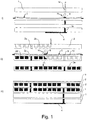
- Fig. 1 shows a schematized and simplified illustration of certain steps of the method according to the invention. As mentioned, the method comprises the steps described in the following.
- a0 all used green sheets 1, 2, and 3 are tempered by removing at least parts of solvent from them.
- Those green sheets form an unsintered ceramic entity, i.e. a ceramic plate which has not been otherwise processed by the method.
- green sheets are available in different standard dimensions. Tempering the green sheets has a positive effect later during the process, at step c) of stencil printing and drying, and during a second optional step of laser cleaning d0).
- step of drying means exposure of the raw ceramic entity to heat, the layers shrink due to evaporation of solvents. It has been noticed that this shrinkage of green sheets does not take place uniformly throughout its extension but the rate is different at the edges as compared to the middle of the green sheets. This causes undesired deformations of the green sheet surface, which may have an impact on the whole module to be manufactured.
- parts of solvents are extracted from the green sheet, thus yielding later a more uniform, reduced shrinkage of the green sheets.
- Part i) shows steps a) and c) of green sheets having no channels.
- holes 1a also called via-holes
- P through-contacts
- step c) they are filled with metallizations resulting in through-contacts 1b.
- the printing head (H) must work the metallization paste 6 forward and backward over the stencil.
- These through-contacts are needed to connect the coil to the pad 4 of the sensor element.
- Part ii) of the figure corresponds to step b), c) and d0) of green sheets having channels.
- channels 2b and through holes 2a are formed by means of lasering (L) in the green sheet 2.
- step b) of forming channels 2b is carried out gradually in multiple lasering sub-steps until uniform channel depth is obtained.
- step c) empty holes 2a and empty channels 2b are filled by stencil printing through a stencil 5 by means of a printing head (H) with metallization paste 6.
- H printing head
- step d0 residual metallization paste between neighboring channels is removed by a laser (L).
- a step of stacking the green sheets (as shown in Fig. 1 iii) one above the other and aligning them to one another is carried out after the optional step d0) of laser cleaning in order to form the raw ceramic entity.
- the step of adding the thin additional green sheet 3 without metallization as outermost green sheet is carried out before sintering the raw ceramic entity in order to protect the electrical passive component or the electrical circuit "buried" in the inner layers.
- channels and holes filled with metallization paste 6 will be referred to by 2d and 2c, respectively, in order to differentiate from empty channels and holes 2b, 2c.
- step d0 the residual metallization paste 2e on the surfaces between the filled channels 2d is removed by means of laser (L), wherein the above mentioned UV-laser, particularly the diode-pumped solid state laser, is used for this task due to the same reasons as mentioned in connection with step b).
- L laser
- This step gains more importance the higher the level of miniaturization is. For example, in case of inter-channel spaces of 30 ⁇ m or below, metallization paste residuals can remain on the surface of the green sheet 2 between two adjacent channels 2d, therefore leading to short-circuits. These metallization paste residuals are removed by the cleaning process, wherein the cleaning time is significantly below one second per coil.
- Part iii) shows an exemplary stack of layers, of which outermost layer 3 is a protective layer.
- the following two layers represent a circuit or a passive electrical component with channels 2d and holes 2c already filled with metallization paste 6.
- the subsequent two layers show exemplarily optional layers having only filled holes 1b, e.g. for establishing electrical contact to the external sensor electronics.
- At least two pads 4 are printed on one side of the coil for connection to the sensor electronics.
- the illustration of iii) shows a stage in which the already prepared layers are ready to be stacked (whereas the gaps between the layers shown in the figures are only for illustrative purposes) and are ready to enter step d).
- step d) the raw ceramic entities are aligned, stacked, laminated and sintered for creating the final tile before separating the single coils.
- integrating high amounts of metallization paste 6 into a ceramic layer or multilayer commonly results in warping or in defects during a standard firing process (sintering process). These undesired effects occur due to differences in shrinkage rate and absolute shrinkage of the metallization paste 6 and the dielectric base material of the green sheets. Other reasons are the diffusion of the metal of the metallization paste (e.g. silver) into the ceramic base material of the green sheet, leading to non-uniform shrinkage of the ceramic, and therefore to creation of defects.
- the metal of the metallization paste e.g. silver
- the current method uses a constrained sintering process which differs from the standard sintering process (unconstrained sintering). It is preferably carried out under pressure. It has been found that a pressure of around 0.1 MPa to 0.8 MPa is sufficient for good results. Other pressures may however also be applied.
- a step e) the coils are separated by sawing, laser cutting, or scribing and breaking in order to create the final sensing element.
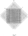
- the contour of the sensing entity must be chosen carefully, e.g. an octagon for sawing as described in Fig. 7 .
- alignment marks are printed around each coil.
- Fig. 2 shows a stencil 5 used for step c) of the method according to the invention.
- the stencil 5 comprises openings 10 (for channels 2b) and openings 9 (for holes 2a) such that metallization paste 6 can be introduced into the empty channels 2b and the empty holes 2a via the printing head (H).
- the equi-spaced openings 10 of the stencil 5 are arranged section-wise along the stencil 5 in order to improve stability of the stencil.
- Metallization paste 6 pushed into two adjacent openings 10 will also fill channel sections which are covered by stencil material between two adjacent stencil openings 10.
- the stencil 5 comprises a polymer structure layer for regulating the amount of metallization paste 6 to be filled in the channels 2b and holes 2a.
- the metallization paste 6 is a conductive paste with a defined solid phase, e.g. silver with solvent. Through holes 2a and channels 2b are filled simultaneously. In order to ensure a uniform filling of the channels with metallization paste 6 the printing head (H) ideally has to be moved forward and backward in several directions in the horizontal plane.
- Fig. 3 shows a perspective view of a coil 11 according to the invention and Fig. 4 shows a top view on the coil of Fig. 3 .
- the coil 11 may be regarded as a sensing element 12 manufactured by means of the described method. If additional layers to the coil layer(s) are present, the coil forms the passive electrical component of the sensing element 12.
- the coil 11 consists of two coil layers 11a and 11b corresponding to two green sheets 2 as shown in Fig. 1 . For reasons of simplicity only the metallization paths forming the coil winding are shown.
- contacts 4 for connecting the coil 11 to the sensor electronics are provided, wherein one contact is connected to one end of the winding of the coil 11 and the other contact is connected to the other end of the winding of the coil 11, as known.
- the coil is a double-D flat coil or a double-D saddle-shaped coil.
- other coil geometries may readily be manufactured.
- a coil may be implemented on one single layer or multiple layers, either as a two-dimensional coil or a three-dimensional coil, depending on the required geometry. Examples of coil shapes and more details about such coils can be found in the above mentioned international patent application WO2015027348 .
- Fig. 5 shows a side view of the coil of Fig. 4 as viewed perpendicularly on the plane AA of Fig. 4 and Fig. 6 shows a cross-section view of the detail B of Fig. 5 .
- the coil is arranged on two green sheet layers.
- the metallizations 2d of the coil 11 have an aspect ratio larger than 1.
- the aspect ratio is defined by depth T of the channel 2d divided by its width W, yielding for the present case T/W > 1.
- each channel 2d ranges between 80 und 120 ⁇ m in a non-sintered green sheet with a thickness of 165 ⁇ m.
- the channel depth T depends on the advised metallization thickness and is controlled precisely by lasering steps during the forming process in order to yield uniformly deep channels over the entire structure.
- This channel depth T predominantly determines the internal resistance of the metallization structure.
- the residual green sheet thickness R remaining after channel formation (as the case may be during multiple sub-steps of step b) mostly determines the distance between metallization of the different coil layers, and therefore influences the inductivity and capacity of the coil 11.
- each filled channel 11a and 11b for the metallizations is about 70 ⁇ m.
- the distance D between two neighboring filled channels of 11a and 11b (channel interspaces or winding interspaces 2g ranges between 20 und 30 ⁇ m.
- Fig. 7 shows an example of a structured tile 8 ready for sawing, laser cutting, or scribing-and-breaking along the separation lines 8a.
- Four different directions are followed, horizontal, vertical, +45° and -45° in order to obtain an octagonal sensing module 12 containing the sensing element 11.
- Fig. 8 shows a perspective view of a sensor module 12 according to the invention and Fig. 9 shows a top view of the module of Fig. 8 as transparent illustration.
- the sensor module 12 comprises a coil 11, visible in Fig. 9 and indicated by the layers 11b.
- the sensor module 12 comprises further green sheets in addition to the two green sheets 2.
- Outermost green sheets 3 and two green sheets 1 of the sensor module sandwich in between the (coil layer) two green sheet 2. They are intended for protection of the coil, as mentioned before.
- Connector holes 1b are provided in green sheet(s) 1.
- Electrically conductive connector surfaces 4 for the coil 11, used for connecting the sensor module 12 to the sensor electronics, are printed on the outmost green sheet layer 1. This becomes apparent when viewing the connectors 4 in connection with the connector holes 1b of Fig. 3 . It is understood that further layers may be arranged between the coil layers 2 and the outermost layer 1.
- the connector surfaces are arranged on one side of the sensor module 12 in the outermost green sheet 1, as shown in Fig. 8 . Therefore, the outermost surface 3 which is not visible in Fig. 8 is a plain green sheet with neither channels nor holes. It is however also possible to arrange one connector surface 4 on one side of the coil 11 and the other connector surface 4 on the other side of the coil 11.
- the sensor module 12 has a minimum diameter of 3 mm, preferably a diameter of 3.7 mm.
- a maximum diameter is not given as there is no particular restriction on this parameter. The only limitation is given by the application where the sensor module 12 is used and by limitations of the manufacturing process.
- the sensor module 12 is manufactured by the described method in the way set forth.
- step a) green sheets 1 only containing through holes are punched in order to create the through-contacts for electrically connecting the coil 11 to an external circuit. Step a) is not required for the outermost layer 3.
- Steps b) and c) and optional step d0) are applied in a similar way to green sheets 2 intended for the coil 11. Steps b) and optional step d0) are not required for layer 1 and steps b) and c) and optional step d0) are not required for layer 3.
- step d Before the sintering of step d), the already mentioned steps of aligning, stacking and lamination of all green sheets is performed. The result is a very compact and robust sensor module. This allows usage of the sensor module in harsh environments.
- the method according to the invention is carried out for in accordance with the type of layer used. Therefore, suitable controlling procedures and software are used to adapt the method to the particular requirements, e.g. to skip one or more steps for layers which don't require the one or more steps. Furthermore, the said controlling software may trigger repeating of individual steps of the method before subsequent steps are executed, e.g. step b) of forming channels (2b), which is carried out gradually in at least three sub-steps. In embodiments the controlling software may also trigger "parking" green sheets until they are used.
- step a0) is carried out for a plurality of layers which include green sheets requiring through-holes and channels and also green sheets not requiring these steps
- the latter green sheets may be "parked" until the layers requiring channels and through-holes have been processed according to steps a) to d). Only after this processing the parked green sheets are introduced into the process again for the step e) of stacking, etc. This is preferred such that all layers experience the same shrinkage in a common process step. However it would be possible to process the parked sheets individually, although not preferred.
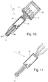
- Fig. 10 shows a sensor device 15 according to the invention.
- the sensor device 15 is preferably used for determining a speed of an electrically conductive object passing in front of the sensor device 15.
- the object is a blade 23 of a turbocharger impeller 25 (see Fig. 11 ).
- the sensor device 15 comprises a sensor housing 16 and a sensor module 12 arranged at an extremity 20 (sensor tip) of the sensor housing 16 and facing in a direction of expected passing of the electrically conductive object i.e. blade 23.
- the sensor module 12 is connected to sensor electronics 18 for signal processing and data transmission, arranged inside the sensor housing 16.
- the sensor housing 16 further comprises a sensor segment 19, a mounting segment 17 and a connector segment 21 with the mounting segment 17 connecting the sensor segment 19 and the connector segment 21 such they are on opposite sides of the mounting segment 17.
- the mounting segment 17 is preferably formed as a flange.
- the sensor module 12 is arranged inside the sensor tip 20 of the sensor segment 19.
- the sensor module 12 and the sensor electronics 18 are connected to one another by interconnections 18a which are connected to contact pads of the sensor electronics 18 and pads 4 of the sensor module 12.
- the sensor electronics 18 and the contacts 18a are preferably mounted on a supporting element 14 which defines the correct place of the sensor electronics 18, the contacts 18a and thereby also the sensor module 12.
- Fig. 11 shows the supporting element 14 for sensor electronics, which has already been described in the context of Fig. 10 .
- Fig. 12 shows a part of a turbocharger 22 according to the invention with the sensor device 15 of Fig. 10 .
- the turbocharger 22 comprises a casing 24, a compressor wheel 25 with compressor wheel blades 23, particularly made of electrical conductive material, particularly titanium, nickel or aluminum, and a sensor device 15, wherein the sensor tip 20 of the sensor device 15 faces the compressor wheel blades 23.
- the thickness of the compressor wheel blades 23 is equal to or larger than 0.2 mm.
- the turbocharger 22 further comprises a compressor inlet 29 inside the casing 24.
- the compressor wheel 25 is connected to a turbine wheel by a shaft (not shown).
- the casing 24 is provided with a recess in form of a hole 26, in particular a cylindrical hole such as a bore hole, that preferably passes entirely through the wall of the turbocharger casing 24 in the direction toward (the blades 23 of) the compressor wheel 25.
- the sensor device 15 of the invention is inserted into the cylindrical through-hole 26, which is tapered to accommodate the diameter of the shaft-like sensor segment 19, (but which narrows to a smaller cylindrical diameter at the tip of the sensor device)until its mounting segment 17 abuts on the wall of the turbocharger casing 24 from the outside.
- the sensor device is fixed to the compressor housing by means of a M4 threaded bolt which is inserted through a hole in the mounting segment 17 and screwed into a corresponding bore mounting in the compressor housing.
- the connector segment 21 points away from the turbocharger casing 24.
- the distal end of the sensor segment 19 with the sensor module 12 is located at the inside opening of the cylindrical hole 26 such that the rotating blades 23 pass by it at a short distance.
- the outer diameter of the sensor segment 19 basically corresponds to the inner diameter of the cylindrical hole 26 such that the sensor segment 19 tightly fits into the cylindrical hole 26.
- an annular sealing element 27 surrounds the sensor device 15 inside the cylindrical hole 26 to provide a secure and tight fit of the sensor device 15 within the cylindrical bore 26.
- the annular sealing element 27 is preferably provided at the transition from the sensor segment 19 to the mounting segment 17.
- the annular sealing element 27 is preferably given by a heat-resistant fluoroelastomer O-ring seal that can withstand temperatures of at least 200°C.
Landscapes
- Engineering & Computer Science (AREA)
- Power Engineering (AREA)
- Mechanical Engineering (AREA)
- General Engineering & Computer Science (AREA)
- Chemical & Material Sciences (AREA)
- Combustion & Propulsion (AREA)
- Manufacturing & Machinery (AREA)
- Microelectronics & Electronic Packaging (AREA)
- Physics & Mathematics (AREA)
- General Physics & Mathematics (AREA)
- General Chemical & Material Sciences (AREA)
- Chemical Kinetics & Catalysis (AREA)
- Ceramic Engineering (AREA)
- Inorganic Chemistry (AREA)
- Measurement Of Length, Angles, Or The Like Using Electric Or Magnetic Means (AREA)
- Coils Or Transformers For Communication (AREA)
- Measuring Oxygen Concentration In Cells (AREA)
Claims (21)
- Procédé de fabrication d'un élément de détection (12) comprenant au moins un composant électrique passif comprenant une bobine (11), comprenant les étapes suivantes :a) perforer de trous (1a) pour des contacts traversants dans au moins une feuille verte (1), les contacts traversants faisant partie du composant électrique passif (11),b) former des canaux (2b) et des contacts traversants (2a) au moyen d'un marquage au laser d'au moins une feuille verte (2) destinée à recevoir la pâte de métallisation (6), les canaux métallisés et les trous traversants (2d, 2c) faisant partie de la bobine (11),c) impression au pochoir et séchage des feuilles vertes (1, 2), y compris la pâte de métallisation (6) dans les canaux (2b) et les trous (1a, 2a) pour créer les canaux métallisés (2d) et les trous métallisés de passage (1b, 2c),d) aligner, empiler, laminer et fritter toutes les feuilles vertes (1, 2, 3) ensemble pour créer un carreau fritté (8) comprenant des bobines (11), ete) séparer les bobines individuelles du carreau fritté (8) afin d'obtenir l'élément de détection fini 12.
- Procédé selon la revendication 1, dans lequel, avant l'étape a), on effectue une étape préliminaire a0) consistant à tempérer toutes les feuilles vertes utilisées (1, 2, 3) en éliminant au moins une partie du solvant de toutes ces feuilles vertes (1, 2, 3).
- Procédé selon la revendication 1 ou 2, dans lequel une étape d0) de nettoyage au laser des surfaces par élimination de la pâte de métallisation résiduelle (2e) entre les canaux métallisés (2d) est effectuée entre les étapes c) et d).
- Procédé selon la revendication 1 ou 2 et la revendication 3, dans lequel l'étape b) de formation de canaux (2b) et/ou l'étape ii) d'élimination de la pâte de métallisation résiduelle (2e) par nettoyage au laser de la surface entre les canaux métallisés (2d) est effectuée au moyen d'un laser UV, en particulier au moyen d'un laser à solide pompé par diode.
- Procédé selon la revendication 1 ou 2, dans lequel l'étape b) de formation des canaux (2b) est réalisée progressivement en au moins trois sous-étapes jusqu'à ce que les canaux (2b) soient entièrement formés, en particulier en trois sous-étapes, dans lequel, dans chaque sous-étape, au moins une partie de la matière en feuille verte des canaux (2b) est enlevée au moyen d'un laser.
- Procédé selon l'une des revendications précédentes, dans lequel l'étape c) d'impression au pochoir est réalisée au moyen d'un pochoir (5) comprenant une couche de structure polymère pour régler une quantité de pâte de métallisation (6) à imprimer dans les canaux (2b) et les trous (2a), avec des premières ouvertures (10, 9) correspondant à des sections des canaux (2b) et/ou des trous (2a), et une couche de support comme support pour la couche de structure polymère, avec des secondes ouvertures correspondant aux premières ouvertures (10, 9) de la couche de structure polymère, dans lequel l'impression est réalisée en remplissant la pâte de métallisation (6) dans les canaux (2b) et/ou les trous (2a) à travers les ouvertures (9, 10) de la couche de structure polymère et de la couche de support.
- Procédé selon l'une des revendications précédentes, dans lequel le frittage de l'étape d) est effectué sous pression, en particulier dans lequel une pression d'environ 0,1 MPa à 0,8 MPa est appliquée.
- Procédé selon l'une des revendications précédentes, dans lequel, dans le cas de la fabrication d'un module de capteur (12) comprenant une pluralité de feuilles vertes (1, 2, 3), une étape d'alignement et d'empilage des feuilles vertes (1, 2, 3) est effectuée après l'étape d'impression au pochoir afin de former l'entité céramique brute.
- Procédé selon l'une des revendications précédentes, dans lequel une feuille verte (3) située le plus à l'extérieur présente ni des canaux métallisés ni des trous traversants métallisés.
- Bobine (11) comme élément de détection (12) fabriquée selon le procédé selon l'une des revendications précédentes, dans lequel la bobine (11) s'étend sur au moins une feuille verte (2) avec des canaux métallisés et des trous de passage métallisés (2c, 2d), dans lequel un canal métallisé et/ou au moins un trou de passage métallisé d'une feuille verte (2) est relié électriquement à un canal métallisé et/ou au moins un trou de passage métallisé d'autres feuilles vertes (1 et/ou 2) ou à des plots (4) au moyen d'au moins un contact de trou de passage électriquement conducteur (2c ou 1b), toutes les métallisations des feuilles vertes (1 et/ou 2) formant avec au moins deux plots (4) la bobine (11) .
- Bobine selon la revendication 10, dans laquelle les métallisations de la bobine (11) ont un rapport d'aspect supérieur à 1, en particulier dans laquelle une profondeur (T) de chaque canal (2b, 2d) est comprise entre 80 et 120 µm, et une largeur (W) de chaque canal (2b, 2d) qui est de 70 µm dans une feuille verte (2) de 165 µm d'épaisseur.
- Bobine selon la revendication 10 ou 11, dans laquelle une distance (D) entre deux canaux voisins (2b, 2d) de l'enroulement de la bobine est comprise entre 20 et 30 µm.
- Bobine selon l'une des revendications 10 à 12, dans laquelle la bobine (11) est une bobine double D ou une bobine en selle double D.
- Module de capteur (12) fabriqué par le procédé selon l'une des revendications 1 à 9, comprenant-une bobine (11) selon l'une des revendications 10 à 13, dans lequel le module de capteur (12) comprend d'autres feuilles vertes (1, 3) en plus des deux feuilles vertes (2) de la bobine (11), dans lequel la feuille verte la plus extérieure (3) du module de capteur (12) ne comprend pas de canaux métallisés et/ou de trous métallisés traversants et dans lequel les feuilles vertes (2) de la bobine (11) sont disposées entre les feuilles vertes les plus extérieures (1, 3) du module de capteur (12).
- Module de capteur selon la revendication 14, dans lequel des trous de connexion (1b, 2c) sont prévus, en particulier dans lequel les trous de connexion (1b, 2c) sont prévus dans au moins une des feuilles vertes (1) qui ne comprennent pas de canaux, dans lequel des plots (4) de la bobine (11), utilisés pour connecter le module de capteur (11) à un circuit électrique (18), sont disposés dans les trous de connexion (1b, 2c) et chaque plot (4) est connecté à une extrémité de l'enroulement de la bobine au moyen de contacts traversants (1b, 2c).
- Module de capteur selon la revendication 15, dans lequel les plots (4) sont situés sur un côté du module de capteur (12) sur la feuille verte la plus extérieure (1).
- Module de capteur selon l'une des revendications 14 à 16, dans lequel le module de capteur (12) a un diamètre minimum de 3 mm, en particulier un diamètre de 3,7 mm.
- Dispositif de capteur (15) pour déterminer la vitesse d'un objet électriquement conducteur (23) passant devant le dispositif de capteur (15), comprenant un boîtier de capteur (16), un module de capteur (12) selon l'une des revendications 14 à 17, dans lequel le module de capteur (12) est disposé à une pointe de capteur (20) du boîtier de capteur (16) et est orienté dans une direction de passage prévue d'un objet électriquement conducteur (23), dans lequel le module de capteur (12) est relié à un circuit électrique (18) disposé à l'intérieur du boîtier de capteur (16) pour le traitement de signaux et la transmission de données.
- Turbocompresseur (22) comprenant une carcasse (24), une roue de compresseur (25) avec des aubes de roue de compresseur (23), en particulier en matériau électriquement conducteur, notamment en titane, en nickel ou en aluminium, et un dispositif de capteur (15) selon la revendication 18, dans lequel la pointe de capteur (20) du dispositif de capteur (15) est orientée vers les aubes de roue de compresseur (23).
- Turbocompresseur selon la revendication 19, dans lequel l'épaisseur des aubes de roue de compresseur (23) est égale ou supérieure à 0,2 mm.
- Utilisation du dispositif de capteur (15) selon la revendication 18 comme capteur de vitesse pour les turbocompresseurs de véhicules, en particulier les véhicules tout-terrain ou les voitures particulières ou les poids lourds, ou pour les turbines d'avion ou pour les turbines génératrices de courant ou pour les machines de forage.
Applications Claiming Priority (2)
| Application Number | Priority Date | Filing Date | Title |
|---|---|---|---|
| CH792016 | 2016-01-20 | ||
| PCT/CH2017/000005 WO2017124200A2 (fr) | 2016-01-20 | 2017-01-11 | Procédé de fabrication pour un élément de détection et dispositif de détection |
Publications (2)
| Publication Number | Publication Date |
|---|---|
| EP3406113A2 EP3406113A2 (fr) | 2018-11-28 |
| EP3406113B1 true EP3406113B1 (fr) | 2020-09-09 |
Family
ID=59361123
Family Applications (1)
| Application Number | Title | Priority Date | Filing Date |
|---|---|---|---|
| EP17729759.5A Active EP3406113B1 (fr) | 2016-01-20 | 2017-01-11 | Procédé de fabrication pour un élément de détection et dispositif de détection |
Country Status (4)
| Country | Link |
|---|---|
| US (1) | US20180330874A1 (fr) |
| EP (1) | EP3406113B1 (fr) |
| CN (1) | CN108781510B (fr) |
| WO (1) | WO2017124200A2 (fr) |
Families Citing this family (5)
| Publication number | Priority date | Publication date | Assignee | Title |
|---|---|---|---|---|
| JP5765855B2 (ja) * | 2012-08-02 | 2015-08-19 | ヤンマー株式会社 | 回転速度検出装置 |
| GB2566053A (en) | 2017-08-31 | 2019-03-06 | Weston Aerospace Ltd | Sensor and method of manufacturing same |
| JP6848944B2 (ja) * | 2018-08-30 | 2021-03-24 | 日亜化学工業株式会社 | 配線基板の製造方法および配線基板 |
| US11365691B2 (en) * | 2019-09-05 | 2022-06-21 | Pratt & Whitney Canada Corp. | Blade angle position feedback system with embedded markers |
| CN111785508B (zh) * | 2020-05-25 | 2022-01-18 | 宁波保诚电气有限公司 | 一种绕线机 |
Family Cites Families (40)
| Publication number | Priority date | Publication date | Assignee | Title |
|---|---|---|---|---|
| US3956052A (en) * | 1974-02-11 | 1976-05-11 | International Business Machines Corporation | Recessed metallurgy for dielectric substrates |
| US4578279A (en) * | 1981-05-26 | 1986-03-25 | International Business Machines Corporation | Inspection of multilayer ceramic circuit modules by electrical inspection of unfired green sheets |
| US4443278A (en) * | 1981-05-26 | 1984-04-17 | International Business Machines Corporation | Inspection of multilayer ceramic circuit modules by electrical inspection of green specimens |
| JPS5893862U (ja) * | 1981-12-21 | 1983-06-25 | 日本特殊陶業株式会社 | 酸素センサ |
| US4581098A (en) * | 1984-10-19 | 1986-04-08 | International Business Machines Corporation | MLC green sheet process |
| JPS63181400A (ja) * | 1987-01-22 | 1988-07-26 | 松下電器産業株式会社 | セラミツク多層基板 |
| US6073339A (en) * | 1996-09-20 | 2000-06-13 | Tdk Corporation Of America | Method of making low profile pin-less planar magnetic devices |
| US20010001406A1 (en) * | 1998-02-17 | 2001-05-24 | Michael James Liberatore | Method of making transmission lines and buried passive components in green tape |
| US6207234B1 (en) * | 1998-06-24 | 2001-03-27 | Vishay Vitramon Incorporated | Via formation for multilayer inductive devices and other devices |
| US6240622B1 (en) * | 1999-07-09 | 2001-06-05 | Micron Technology, Inc. | Integrated circuit inductors |
| JP3621300B2 (ja) * | 1999-08-03 | 2005-02-16 | 太陽誘電株式会社 | 電源回路用積層インダクタ |
| KR100328710B1 (ko) * | 1999-08-23 | 2002-03-20 | 박종섭 | 인덕터 및 그의 제조방법 |
| JP3436735B2 (ja) * | 1999-10-01 | 2003-08-18 | 日本碍子株式会社 | 圧電/電歪デバイス及びその製造方法 |
| JP2001244123A (ja) * | 2000-02-28 | 2001-09-07 | Kawatetsu Mining Co Ltd | 表面実装型平面磁気素子及びその製造方法 |
| JP2001257471A (ja) * | 2000-03-10 | 2001-09-21 | Ngk Insulators Ltd | 多層配線基板及びその製造方法 |
| US6480395B1 (en) * | 2000-05-25 | 2002-11-12 | Hewlett-Packard Company | Device and method for interstitial components in a printed circuit board |
| WO2001091166A1 (fr) * | 2000-05-26 | 2001-11-29 | Ibiden Co., Ltd. | Dispositif de fabrication et de controle d'un semi-conducteur |
| JP3473601B2 (ja) * | 2000-12-26 | 2003-12-08 | 株式会社デンソー | プリント基板およびその製造方法 |
| JP3642026B2 (ja) * | 2001-01-12 | 2005-04-27 | 株式会社村田製作所 | 加速度センサおよびその製造方法 |
| CN1586018A (zh) * | 2001-09-11 | 2005-02-23 | 日本碍子株式会社 | 压电/电致伸缩器件的制作方法 |
| US6961487B2 (en) * | 2003-04-14 | 2005-11-01 | Agilent Technologies, Inc. | Method and structure for a pusher-mode piezoelectrically actuated liquid metal optical switch |
| US7014727B2 (en) * | 2003-07-07 | 2006-03-21 | Potomac Photonics, Inc. | Method of forming high resolution electronic circuits on a substrate |
| KR100688858B1 (ko) * | 2004-12-30 | 2007-03-02 | 삼성전기주식회사 | 스파이럴 3차원 인덕터를 내장한 인쇄회로기판 및 그 제조방법 |
| WO2007049788A1 (fr) * | 2005-10-28 | 2007-05-03 | Hitachi Metals, Ltd. | Convertisseur cc/cc |
| JP4509186B2 (ja) * | 2006-01-31 | 2010-07-21 | 日立金属株式会社 | 積層部品及びこれを用いたモジュール |
| KR100763837B1 (ko) * | 2006-07-18 | 2007-10-05 | 삼성전기주식회사 | 인쇄회로기판 제조방법 |
| JP2010515281A (ja) * | 2007-01-02 | 2010-05-06 | オルメット サーキッツ、インコーポレイテッド | 並列加工された回路および充填ビアから高密度の多層プリント配線基板を作成する方法 |
| JP2009027033A (ja) * | 2007-07-20 | 2009-02-05 | Tdk Corp | 積層型複合電子部品 |
| JP5195758B2 (ja) * | 2007-09-14 | 2013-05-15 | 株式会社村田製作所 | 積層コイル部品およびその製造方法 |
| CN101889319B (zh) * | 2007-12-25 | 2013-01-02 | 日立金属株式会社 | 叠层电感器以及使用该叠层电感器的功率转换装置 |
| US20110095856A1 (en) * | 2008-05-09 | 2011-04-28 | Taiyo Yuden Co., Ltd. | Multi layer inductor and method for manufacturing the same |
| KR101555379B1 (ko) * | 2008-06-30 | 2015-09-23 | 니혼도꾸슈도교 가부시키가이샤 | 전기검사용 기판 및 그 제조방법 |
| CN102099876A (zh) * | 2008-07-15 | 2011-06-15 | 株式会社村田制作所 | 电子元器件 |
| JP5382225B2 (ja) * | 2010-07-29 | 2014-01-08 | 株式会社村田製作所 | セラミック多層基板およびその製造方法 |
| JP5463235B2 (ja) * | 2010-07-30 | 2014-04-09 | 日立オートモティブシステムズ株式会社 | 車載用電子機器に用いる基板構造 |
| JP5576843B2 (ja) * | 2010-12-15 | 2014-08-20 | 日本特殊陶業株式会社 | 導体パターン印刷用インク |
| KR101603827B1 (ko) * | 2011-06-15 | 2016-03-16 | 가부시키가이샤 무라타 세이사쿠쇼 | 적층 코일 부품 |
| JP5401617B1 (ja) * | 2013-01-24 | 2014-01-29 | 有限会社 ナプラ | 受動素子内蔵基板 |
| US10379134B2 (en) * | 2013-08-29 | 2019-08-13 | Jaquet Technology Group Ag | Sensor device for determining rotational speed of a rotatable object and turbocharger with such a sensor device |
| CN107209432B (zh) * | 2014-12-19 | 2021-09-03 | 唯景公司 | 减少电致变色装置中汇流条下方的缺陷 |
-
2017
- 2017-01-11 EP EP17729759.5A patent/EP3406113B1/fr active Active
- 2017-01-11 WO PCT/CH2017/000005 patent/WO2017124200A2/fr not_active Ceased
- 2017-01-11 CN CN201780006948.XA patent/CN108781510B/zh not_active Expired - Fee Related
-
2018
- 2018-07-20 US US16/040,699 patent/US20180330874A1/en not_active Abandoned
Non-Patent Citations (1)
| Title |
|---|
| None * |
Also Published As
| Publication number | Publication date |
|---|---|
| WO2017124200A3 (fr) | 2017-09-28 |
| US20180330874A1 (en) | 2018-11-15 |
| CN108781510A (zh) | 2018-11-09 |
| CN108781510B (zh) | 2021-08-17 |
| WO2017124200A2 (fr) | 2017-07-27 |
| EP3406113A2 (fr) | 2018-11-28 |
Similar Documents
| Publication | Publication Date | Title |
|---|---|---|
| EP3406113B1 (fr) | Procédé de fabrication pour un élément de détection et dispositif de détection | |
| KR100451955B1 (ko) | 세라믹 다층 기판의 제조방법 및 미소성의 복합 적층체 | |
| US8914974B2 (en) | Method for integrating an electronic component into a printed circuit board | |
| CN105518467B (zh) | 传感器设备以及具有该传感器设备的涡轮增压器 | |
| CN101943675A (zh) | 片式宽域标准信号输出车用氧传感器 | |
| US10797003B2 (en) | Circuit module | |
| CN201757743U (zh) | 片式宽域标准信号输出车用氧传感器 | |
| JP5673064B2 (ja) | コイル内蔵基板の製造方法 | |
| WO2006040959A1 (fr) | Procédé de fabrication de composants électroniques céramiques stratifiés et dispositif de production correspondant | |
| EP3370049B1 (fr) | Substrat de capteur et module de détection | |
| JP2011018783A (ja) | 多層セラミック基板の製造方法 | |
| Ihle et al. | Low temperature co-fired ceramics technology for active eddy current turbocharger speed sensors | |
| JP2004186342A (ja) | セラミック積層体及びその製法 | |
| JP4413375B2 (ja) | キャパシタ内蔵インターポーザ及びその製造方法 | |
| CN222461378U (zh) | 一种陶瓷芯片及氮氧传感器 | |
| US20260128229A1 (en) | Multilayer ceramic capacitor | |
| JP2004179528A (ja) | セラミック積層体の製法 | |
| JP2010251516A (ja) | 多層セラミック基板の製造方法と、多層セラミック基板を用いた空気流量計 | |
| JP4442351B2 (ja) | セラミック多層基板およびその製造方法 | |
| JP2004186344A (ja) | セラミック積層体及びその製法 | |
| JP2008071843A (ja) | 多層セラミック基板及びその製造方法 | |
| KR100349121B1 (ko) | 램버스용 인쇄회로기판의 층간 절연거리 측정방법 | |
| JP2004063910A (ja) | セラミック積層体の製法 | |
| JP2010258175A (ja) | セラミック基板の製造方法 | |
| JP2004179529A (ja) | セラミック積層体の製法 |
Legal Events
| Date | Code | Title | Description |
|---|---|---|---|
| STAA | Information on the status of an ep patent application or granted ep patent |
Free format text: STATUS: UNKNOWN |
|
| STAA | Information on the status of an ep patent application or granted ep patent |
Free format text: STATUS: THE INTERNATIONAL PUBLICATION HAS BEEN MADE |
|
| PUAI | Public reference made under article 153(3) epc to a published international application that has entered the european phase |
Free format text: ORIGINAL CODE: 0009012 |
|
| STAA | Information on the status of an ep patent application or granted ep patent |
Free format text: STATUS: REQUEST FOR EXAMINATION WAS MADE |
|
| 17P | Request for examination filed |
Effective date: 20180813 |
|
| AK | Designated contracting states |
Kind code of ref document: A2 Designated state(s): AL AT BE BG CH CY CZ DE DK EE ES FI FR GB GR HR HU IE IS IT LI LT LU LV MC MK MT NL NO PL PT RO RS SE SI SK SM TR |
|
| AX | Request for extension of the european patent |
Extension state: BA ME |
|
| RIN1 | Information on inventor provided before grant (corrected) |
Inventor name: TUOR, ANDREAS Inventor name: IHLE, MARTIN Inventor name: HIRSCH, OLIVER Inventor name: ZIESCHE, STEFFEN |
|
| DAV | Request for validation of the european patent (deleted) | ||
| DAX | Request for extension of the european patent (deleted) | ||
| GRAP | Despatch of communication of intention to grant a patent |
Free format text: ORIGINAL CODE: EPIDOSNIGR1 |
|
| STAA | Information on the status of an ep patent application or granted ep patent |
Free format text: STATUS: GRANT OF PATENT IS INTENDED |
|
| RIC1 | Information provided on ipc code assigned before grant |
Ipc: G01P 3/49 20060101ALI20200316BHEP Ipc: H05K 1/16 20060101AFI20200316BHEP Ipc: F02B 39/00 20060101ALI20200316BHEP Ipc: F02B 39/16 20060101ALI20200316BHEP Ipc: H05K 3/40 20060101ALN20200316BHEP Ipc: H05K 3/26 20060101ALN20200316BHEP Ipc: H05K 3/46 20060101ALI20200316BHEP Ipc: F04D 27/00 20060101ALI20200316BHEP Ipc: H05K 3/10 20060101ALN20200316BHEP Ipc: H05K 3/12 20060101ALN20200316BHEP Ipc: H05K 3/00 20060101ALN20200316BHEP |
|
| RIC1 | Information provided on ipc code assigned before grant |
Ipc: H05K 3/00 20060101ALN20200407BHEP Ipc: H05K 3/40 20060101ALN20200407BHEP Ipc: H05K 3/46 20060101ALI20200407BHEP Ipc: G01P 3/49 20060101ALI20200407BHEP Ipc: H05K 3/10 20060101ALN20200407BHEP Ipc: H05K 3/12 20060101ALN20200407BHEP Ipc: H05K 3/26 20060101ALN20200407BHEP Ipc: F02B 39/16 20060101ALI20200407BHEP Ipc: F02B 39/00 20060101ALI20200407BHEP Ipc: H05K 1/16 20060101AFI20200407BHEP Ipc: F04D 27/00 20060101ALI20200407BHEP |
|
| INTG | Intention to grant announced |
Effective date: 20200422 |
|
| GRAS | Grant fee paid |
Free format text: ORIGINAL CODE: EPIDOSNIGR3 |
|
| GRAA | (expected) grant |
Free format text: ORIGINAL CODE: 0009210 |
|
| STAA | Information on the status of an ep patent application or granted ep patent |
Free format text: STATUS: THE PATENT HAS BEEN GRANTED |
|
| AK | Designated contracting states |
Kind code of ref document: B1 Designated state(s): AL AT BE BG CH CY CZ DE DK EE ES FI FR GB GR HR HU IE IS IT LI LT LU LV MC MK MT NL NO PL PT RO RS SE SI SK SM TR |
|
| REG | Reference to a national code |
Ref country code: GB Ref legal event code: FG4D |
|
| REG | Reference to a national code |
Ref country code: AT Ref legal event code: REF Ref document number: 1313225 Country of ref document: AT Kind code of ref document: T Effective date: 20200915 Ref country code: CH Ref legal event code: EP |
|
| REG | Reference to a national code |
Ref country code: DE Ref legal event code: R096 Ref document number: 602017023306 Country of ref document: DE |
|
| REG | Reference to a national code |
Ref country code: IE Ref legal event code: FG4D |
|
| REG | Reference to a national code |
Ref country code: LT Ref legal event code: MG4D |
|
| PG25 | Lapsed in a contracting state [announced via postgrant information from national office to epo] |
Ref country code: NO Free format text: LAPSE BECAUSE OF FAILURE TO SUBMIT A TRANSLATION OF THE DESCRIPTION OR TO PAY THE FEE WITHIN THE PRESCRIBED TIME-LIMIT Effective date: 20201209 Ref country code: FI Free format text: LAPSE BECAUSE OF FAILURE TO SUBMIT A TRANSLATION OF THE DESCRIPTION OR TO PAY THE FEE WITHIN THE PRESCRIBED TIME-LIMIT Effective date: 20200909 Ref country code: SE Free format text: LAPSE BECAUSE OF FAILURE TO SUBMIT A TRANSLATION OF THE DESCRIPTION OR TO PAY THE FEE WITHIN THE PRESCRIBED TIME-LIMIT Effective date: 20200909 Ref country code: BG Free format text: LAPSE BECAUSE OF FAILURE TO SUBMIT A TRANSLATION OF THE DESCRIPTION OR TO PAY THE FEE WITHIN THE PRESCRIBED TIME-LIMIT Effective date: 20201209 Ref country code: HR Free format text: LAPSE BECAUSE OF FAILURE TO SUBMIT A TRANSLATION OF THE DESCRIPTION OR TO PAY THE FEE WITHIN THE PRESCRIBED TIME-LIMIT Effective date: 20200909 Ref country code: LT Free format text: LAPSE BECAUSE OF FAILURE TO SUBMIT A TRANSLATION OF THE DESCRIPTION OR TO PAY THE FEE WITHIN THE PRESCRIBED TIME-LIMIT Effective date: 20200909 Ref country code: GR Free format text: LAPSE BECAUSE OF FAILURE TO SUBMIT A TRANSLATION OF THE DESCRIPTION OR TO PAY THE FEE WITHIN THE PRESCRIBED TIME-LIMIT Effective date: 20201210 |
|
| REG | Reference to a national code |
Ref country code: AT Ref legal event code: MK05 Ref document number: 1313225 Country of ref document: AT Kind code of ref document: T Effective date: 20200909 |
|
| REG | Reference to a national code |
Ref country code: NL Ref legal event code: MP Effective date: 20200909 |
|
| PG25 | Lapsed in a contracting state [announced via postgrant information from national office to epo] |
Ref country code: PL Free format text: LAPSE BECAUSE OF FAILURE TO SUBMIT A TRANSLATION OF THE DESCRIPTION OR TO PAY THE FEE WITHIN THE PRESCRIBED TIME-LIMIT Effective date: 20200909 Ref country code: RS Free format text: LAPSE BECAUSE OF FAILURE TO SUBMIT A TRANSLATION OF THE DESCRIPTION OR TO PAY THE FEE WITHIN THE PRESCRIBED TIME-LIMIT Effective date: 20200909 Ref country code: LV Free format text: LAPSE BECAUSE OF FAILURE TO SUBMIT A TRANSLATION OF THE DESCRIPTION OR TO PAY THE FEE WITHIN THE PRESCRIBED TIME-LIMIT Effective date: 20200909 |
|
| PG25 | Lapsed in a contracting state [announced via postgrant information from national office to epo] |
Ref country code: CZ Free format text: LAPSE BECAUSE OF FAILURE TO SUBMIT A TRANSLATION OF THE DESCRIPTION OR TO PAY THE FEE WITHIN THE PRESCRIBED TIME-LIMIT Effective date: 20200909 Ref country code: RO Free format text: LAPSE BECAUSE OF FAILURE TO SUBMIT A TRANSLATION OF THE DESCRIPTION OR TO PAY THE FEE WITHIN THE PRESCRIBED TIME-LIMIT Effective date: 20200909 Ref country code: PT Free format text: LAPSE BECAUSE OF FAILURE TO SUBMIT A TRANSLATION OF THE DESCRIPTION OR TO PAY THE FEE WITHIN THE PRESCRIBED TIME-LIMIT Effective date: 20210111 Ref country code: SM Free format text: LAPSE BECAUSE OF FAILURE TO SUBMIT A TRANSLATION OF THE DESCRIPTION OR TO PAY THE FEE WITHIN THE PRESCRIBED TIME-LIMIT Effective date: 20200909 Ref country code: EE Free format text: LAPSE BECAUSE OF FAILURE TO SUBMIT A TRANSLATION OF THE DESCRIPTION OR TO PAY THE FEE WITHIN THE PRESCRIBED TIME-LIMIT Effective date: 20200909 |
|
| PG25 | Lapsed in a contracting state [announced via postgrant information from national office to epo] |
Ref country code: ES Free format text: LAPSE BECAUSE OF FAILURE TO SUBMIT A TRANSLATION OF THE DESCRIPTION OR TO PAY THE FEE WITHIN THE PRESCRIBED TIME-LIMIT Effective date: 20200909 Ref country code: AL Free format text: LAPSE BECAUSE OF FAILURE TO SUBMIT A TRANSLATION OF THE DESCRIPTION OR TO PAY THE FEE WITHIN THE PRESCRIBED TIME-LIMIT Effective date: 20200909 Ref country code: AT Free format text: LAPSE BECAUSE OF FAILURE TO SUBMIT A TRANSLATION OF THE DESCRIPTION OR TO PAY THE FEE WITHIN THE PRESCRIBED TIME-LIMIT Effective date: 20200909 Ref country code: IS Free format text: LAPSE BECAUSE OF FAILURE TO SUBMIT A TRANSLATION OF THE DESCRIPTION OR TO PAY THE FEE WITHIN THE PRESCRIBED TIME-LIMIT Effective date: 20210109 |
|
| REG | Reference to a national code |
Ref country code: DE Ref legal event code: R097 Ref document number: 602017023306 Country of ref document: DE |
|
| PG25 | Lapsed in a contracting state [announced via postgrant information from national office to epo] |
Ref country code: SK Free format text: LAPSE BECAUSE OF FAILURE TO SUBMIT A TRANSLATION OF THE DESCRIPTION OR TO PAY THE FEE WITHIN THE PRESCRIBED TIME-LIMIT Effective date: 20200909 |
|
| PLBE | No opposition filed within time limit |
Free format text: ORIGINAL CODE: 0009261 |
|
| STAA | Information on the status of an ep patent application or granted ep patent |
Free format text: STATUS: NO OPPOSITION FILED WITHIN TIME LIMIT |
|
| 26N | No opposition filed |
Effective date: 20210610 |
|
| PG25 | Lapsed in a contracting state [announced via postgrant information from national office to epo] |
Ref country code: DK Free format text: LAPSE BECAUSE OF FAILURE TO SUBMIT A TRANSLATION OF THE DESCRIPTION OR TO PAY THE FEE WITHIN THE PRESCRIBED TIME-LIMIT Effective date: 20200909 Ref country code: SI Free format text: LAPSE BECAUSE OF FAILURE TO SUBMIT A TRANSLATION OF THE DESCRIPTION OR TO PAY THE FEE WITHIN THE PRESCRIBED TIME-LIMIT Effective date: 20200909 Ref country code: MC Free format text: LAPSE BECAUSE OF FAILURE TO SUBMIT A TRANSLATION OF THE DESCRIPTION OR TO PAY THE FEE WITHIN THE PRESCRIBED TIME-LIMIT Effective date: 20200909 |
|
| REG | Reference to a national code |
Ref country code: CH Ref legal event code: PL |
|
| GBPC | Gb: european patent ceased through non-payment of renewal fee |
Effective date: 20210111 |
|
| PG25 | Lapsed in a contracting state [announced via postgrant information from national office to epo] |
Ref country code: LU Free format text: LAPSE BECAUSE OF NON-PAYMENT OF DUE FEES Effective date: 20210111 |
|
| REG | Reference to a national code |
Ref country code: BE Ref legal event code: MM Effective date: 20210131 |
|
| PG25 | Lapsed in a contracting state [announced via postgrant information from national office to epo] |
Ref country code: FR Free format text: LAPSE BECAUSE OF NON-PAYMENT OF DUE FEES Effective date: 20210131 Ref country code: IT Free format text: LAPSE BECAUSE OF FAILURE TO SUBMIT A TRANSLATION OF THE DESCRIPTION OR TO PAY THE FEE WITHIN THE PRESCRIBED TIME-LIMIT Effective date: 20200909 |
|
| PG25 | Lapsed in a contracting state [announced via postgrant information from national office to epo] |
Ref country code: LI Free format text: LAPSE BECAUSE OF NON-PAYMENT OF DUE FEES Effective date: 20210131 Ref country code: GB Free format text: LAPSE BECAUSE OF NON-PAYMENT OF DUE FEES Effective date: 20210111 Ref country code: CH Free format text: LAPSE BECAUSE OF NON-PAYMENT OF DUE FEES Effective date: 20210131 |
|
| PG25 | Lapsed in a contracting state [announced via postgrant information from national office to epo] |
Ref country code: IE Free format text: LAPSE BECAUSE OF NON-PAYMENT OF DUE FEES Effective date: 20210111 |
|
| PG25 | Lapsed in a contracting state [announced via postgrant information from national office to epo] |
Ref country code: IS Free format text: LAPSE BECAUSE OF FAILURE TO SUBMIT A TRANSLATION OF THE DESCRIPTION OR TO PAY THE FEE WITHIN THE PRESCRIBED TIME-LIMIT Effective date: 20210109 |
|
| PG25 | Lapsed in a contracting state [announced via postgrant information from national office to epo] |
Ref country code: BE Free format text: LAPSE BECAUSE OF NON-PAYMENT OF DUE FEES Effective date: 20210131 |
|
| PG25 | Lapsed in a contracting state [announced via postgrant information from national office to epo] |
Ref country code: NL Free format text: LAPSE BECAUSE OF NON-PAYMENT OF DUE FEES Effective date: 20200923 Ref country code: CY Free format text: LAPSE BECAUSE OF FAILURE TO SUBMIT A TRANSLATION OF THE DESCRIPTION OR TO PAY THE FEE WITHIN THE PRESCRIBED TIME-LIMIT Effective date: 20200909 |
|
| PG25 | Lapsed in a contracting state [announced via postgrant information from national office to epo] |
Ref country code: HU Free format text: LAPSE BECAUSE OF FAILURE TO SUBMIT A TRANSLATION OF THE DESCRIPTION OR TO PAY THE FEE WITHIN THE PRESCRIBED TIME-LIMIT; INVALID AB INITIO Effective date: 20170111 |
|
| PG25 | Lapsed in a contracting state [announced via postgrant information from national office to epo] |
Ref country code: MK Free format text: LAPSE BECAUSE OF FAILURE TO SUBMIT A TRANSLATION OF THE DESCRIPTION OR TO PAY THE FEE WITHIN THE PRESCRIBED TIME-LIMIT Effective date: 20200909 |
|
| PG25 | Lapsed in a contracting state [announced via postgrant information from national office to epo] |
Ref country code: TR Free format text: LAPSE BECAUSE OF FAILURE TO SUBMIT A TRANSLATION OF THE DESCRIPTION OR TO PAY THE FEE WITHIN THE PRESCRIBED TIME-LIMIT Effective date: 20200909 |
|
| PG25 | Lapsed in a contracting state [announced via postgrant information from national office to epo] |
Ref country code: MT Free format text: LAPSE BECAUSE OF FAILURE TO SUBMIT A TRANSLATION OF THE DESCRIPTION OR TO PAY THE FEE WITHIN THE PRESCRIBED TIME-LIMIT Effective date: 20200909 |
|
| PGFP | Annual fee paid to national office [announced via postgrant information from national office to epo] |
Ref country code: DE Payment date: 20260120 Year of fee payment: 10 |